EP2124266A1 - Verfahren zur Bildung einer Quantentopfstruktur und Verfahren zur Herstellung eines lichtemittierenden Halbleiterelements - Google Patents
Verfahren zur Bildung einer Quantentopfstruktur und Verfahren zur Herstellung eines lichtemittierenden Halbleiterelements Download PDFInfo
- Publication number
- EP2124266A1 EP2124266A1 EP09005065A EP09005065A EP2124266A1 EP 2124266 A1 EP2124266 A1 EP 2124266A1 EP 09005065 A EP09005065 A EP 09005065A EP 09005065 A EP09005065 A EP 09005065A EP 2124266 A1 EP2124266 A1 EP 2124266A1
- Authority
- EP
- European Patent Office
- Prior art keywords
- starting material
- material gas
- layer
- well
- grown
- Prior art date
- Legal status (The legal status is an assumption and is not a legal conclusion. Google has not performed a legal analysis and makes no representation as to the accuracy of the status listed.)
- Granted
Links
Images


Classifications
-
- H10P14/3416—
-
- H—ELECTRICITY
- H10—SEMICONDUCTOR DEVICES; ELECTRIC SOLID-STATE DEVICES NOT OTHERWISE PROVIDED FOR
- H10H—INORGANIC LIGHT-EMITTING SEMICONDUCTOR DEVICES HAVING POTENTIAL BARRIERS
- H10H20/00—Individual inorganic light-emitting semiconductor devices having potential barriers, e.g. light-emitting diodes [LED]
- H10H20/01—Manufacture or treatment
- H10H20/011—Manufacture or treatment of bodies, e.g. forming semiconductor layers
- H10H20/013—Manufacture or treatment of bodies, e.g. forming semiconductor layers having light-emitting regions comprising only Group III-V materials
- H10H20/0137—Manufacture or treatment of bodies, e.g. forming semiconductor layers having light-emitting regions comprising only Group III-V materials the light-emitting regions comprising nitride materials
-
- H10P14/24—
-
- H10P14/2908—
-
- H10P14/2926—
-
- H10P14/3216—
-
- H—ELECTRICITY
- H10—SEMICONDUCTOR DEVICES; ELECTRIC SOLID-STATE DEVICES NOT OTHERWISE PROVIDED FOR
- H10H—INORGANIC LIGHT-EMITTING SEMICONDUCTOR DEVICES HAVING POTENTIAL BARRIERS
- H10H20/00—Individual inorganic light-emitting semiconductor devices having potential barriers, e.g. light-emitting diodes [LED]
- H10H20/80—Constructional details
- H10H20/81—Bodies
- H10H20/811—Bodies having quantum effect structures or superlattices, e.g. tunnel junctions
- H10H20/812—Bodies having quantum effect structures or superlattices, e.g. tunnel junctions within the light-emitting regions, e.g. having quantum confinement structures
Definitions
- the present invention relates to a method for forming a quantum well structure and a method for manufacturing a semiconductor light emitting element.
- group III nitride-based semiconductor light emitting element includes an active layer having a multiquantum well (MQW) structure in which well layers each composed of a group III nitride semiconductor which includes indium (hereinafter referred as "In” in some cases) and another group III element (such as gallium) and barrier layers each composed of GaN or InGaN which has a band gap wider than that of each well layer are alternately laminated to each other.
- MQW multiquantum well
- a starting material gas for In such as trimethylindium
- a starting material gas for the other group III element such as trimethylgallium
- a starting material gas for N such as ammonia
- a technique has been disclosed in which a multiquantum well structure including InGaN well layers and GaN barrier layers is formed by a metal organic chemical vapor deposition (MOCVD) method on a GaN layer which has the (0001) plane as a growth surface and which is formed on a sapphire substrate.
- MOCVD metal organic chemical vapor deposition
- PL photoluminescence
- the band gap of the well layer needs to be narrower than that of the barrier layer, in general, an In composition of the well layer is set higher than that of the barrier layer.
- the variation in the In composition of the well layer in a thickness direction thereof is preferably reduced as small as possible. The reason for this is that when the variation in the In composition in the thickness direction of the well layer is reduced, the band gap value becomes stable along the thickness direction, and the spread of light emission wavelength (half bandwidth of a light emission spectrum) can be suppressed.
- the In composition is insufficient at an early growth stage of the well layer. That is, immediately after the well layer (such as InGaN) starts to grow, In is not sufficiently incorporated right on the barrier layer (such as GaN), and the In composition gradually increases as the well layer grows; hence, a desired In composition is realized when the thickness of the well layer reaches a certain level. Accordingly, the variation in the In composition unfavorably occurs in the thickness direction of the well layer, and as a result, it becomes difficult to suppress the spread of light emission wavelength.
- the light emission wavelength of the well layer is set from a green to a red color wavelength range, such as from 450 nm to 650 nm
- a gallium nitride substrate having a primary surface inclined with the (0001) plane is used; however, when the well layer is formed on a gallium nitride substrate having an off angle as described above, In is not easily incorporated as compared to the growth on the (0001) plane, and as a result, the variation in the In composition apparently occurs in the thickness direction of the well layer.
- the In composition of the well layer is relatively low.
- the variation in the In composition in the thickness direction will rarely cause problems.
- a growth temperature of the well layer and that of the barrier layer are set to be equal to each other.
- the above problem caused by the variation in the In composition in the thickness direction becomes apparent.
- the present invention has been conceived in consideration of the above problem, and an object of the present invention is to provide a method for forming a quantum well layer structure that can reduce the variation in the In composition in a thickness direction of a well layer grown on a gallium nitride substrate having an off-angle and to provide a method for manufacturing a semiconductor light emitting element.
- a method for forming a quantum well structure comprises the step of alternately growing barrier layers and well layers on a primary surface of a gallium nitride substrate which is inclined with respect to the (0001) plane so as to form the quantum well structure, and in the above growing step, the well layers are each formed by growing a group III nitride semiconductor including indium and another group III element, the barrier layers are each grown at a first temperature, the well layers are each grown at a second temperature which is lower than the first temperature, and when the well layers are each grown, a starting material gas for indium is supplied before a starting material gas for the other group III element is supplied.
- a method for manufacturing a semiconductor light emitting element according to the present invention is a method for manufacturing a semiconductor light emitting element having a light emission wavelength of 450 to 650 nm, which comprises the step of alternately growing barrier layers and well layers on a primary surface of a gallium nitride substrate which is inclined with respect to the (0001) plane so as to form a quantum well active layer.
- the well layers are each formed by growing a group III nitride semiconductor including indium and another group III element, the barrier layers are each grown at a first temperature, the well layers are each grown at a second temperature which is lower than the first temperature, and when the well layers are each grown, a starting material gas for indium is supplied before a starting material gas for the other group III element is supplied.
- the starting material gas for the other group III element when the well layers are each grown, before the starting material gas for the other group III element is supplied, the starting material gas for In is supplied. Accordingly, until the starting material gas for the other group III element is supplied, In atoms are migrating on each barrier layer.
- the well layer is continuously grown by starting the supply of the starting material gas for the other group III element, the In atoms migrating at an early growth stage are incorporated in the well layer, and a decrease in the In composition at the early growth stage of the well layer is suppressed; hence, the variation in the In composition in the thickness direction of the well layer formed on the primary surface of the gallium nitride substrate which is inclined with respect to the (0001) plane can be reduced.
- the In composition when the In composition is increased by decreasing the growth temperature (second temperature) of the well layer lower than the growth temperature (first temperature) of the barrier layer, the variation in the In composition in the thickness direction can be particularly effectively reduced; hence, a well layer having a relatively long PL wavelength, such as in the range of 450 to 650 nm, can be preferably formed.
- a starting material gas for nitrogen may be supplied together with the starting material gas for indium.
- In atoms and InN molecules are migrating on each barrier layer. Even by the method as described above, the decrease in the In composition at the early growth stage of the well layer can be suppressed.
- the supply of the starting material gas for indium may be started after a substrate temperature reaches the second temperature. Accordingly, In atoms are effectively migrating on the barrier layer at the early growth stage of the well layer, and the effect described above can be preferably obtained.
- the growth temperature that is, the substrate temperature
- a first temperature t 1 such as 880°C.
- TMG which is the starting material gas for Ga
- NH 3 which is the starting material gas for N
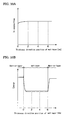
- Figure 8A is a graph showing a theoretical relationship between the light emission wavelength and the thickness of a well layer composed of InGaN.
- a line G12 in the figure the quantum confinement effect decreases as the thickness of the well layer is increased, and the light emission wavelength is increased.
- the band is bent since the piezoelectric field is generated in the thickness direction as the thickness of the well layer is increased, and hence the light emission wavelength is increased as the thickness of the well layer is increased. Accordingly, when these behaviors are combined with each other, the theoretical relationship between the light emission wavelength and the thickness of the well layer is obtained as shown by a line G13 in the figure, and hence it is believed that the light emission wavelength is increased as the thickness of the well layer is increased.
- the In composition when the targeted In composition is low (shown by the line G21), the In composition reaches the targeted value when the thickness is still small, and hence the variation in the In composition in the thickness direction of a well layer having a certain thickness (such as 3 nm) is larger when the targeted In composition is high (line G22) than that when the targeted In composition is low (line G21). Hence, as the targeted In composition is higher, it can be said that the effect obtained by the method of this embodiment is significant.
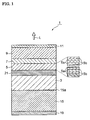
- a GaN substrate (corresponding to the n-type GaN substrate 40 shown in Fig. 3A ) having a primary surface inclined in an a-axis direction by 18° with respect to the c-plane was placed in a reaction furnace, while the pressure inside the reaction furnace was maintained at 27 kPa and a NH 3 gas and a H 2 gas were supplied thereto, a heat treatment was performed for 10 minutes at a temperature of 1,050°C.
- the substrate temperature was decreased to 800°C, and by supplying TMG, TMI, NH 3 , and MMSi to the reaction furnace, an n-type InGaN buffer layer (corresponding to the n-type InGaN buffer layer 42 shown in Fig. 3B ) was grown so as to have a thickness of 50 nm.
- the In composition of the InGaN buffer layer was set to 5%.
- the substrate temperature was increased to 880°C (first temperature t 1 ), and by supplying TMG and NH 3 to the reaction furnace, a GaN barrier layer (corresponding to the barrier layer 43 shown in Fig. 4A ) was grown on the InGaN buffer layer so as to have a thickness of 15 nm.
- a GaN barrier layer (corresponding to the barrier layer 43 shown in Fig. 4A ) was grown on the InGaN buffer layer so as to have a thickness of 15 nm.
- the substrate temperature was decreased to 700°C (second temperature t 2 )
- TMI and NH 3 or only TMI
- an active layer (corresponding to the active layer 50 shown in Fig. 5A ) having a three-period multiquantum well structure was grown.
- the change in substrate temperature and the change in flow rate of the starting material gases in the steps described above are as shown in the parts (A) and (B) of Fig. 6 , respectively.
- the substrate temperature was increased to 1,000°C, and bis(cyclopentadienyl) magnesium (CP 2 Mg) functioning as a p-type doping source was supplied together with TMG, trimethylaluminum (TMA), and NH 3 , so that a p-type AlGaN layer (corresponding to the p-type AlGaN semiconductor layer 51 shown in Fig. 5B ) was grown so as to have a thickness of 20 nm.
- TMA trimethylaluminum
- NH 3 NH 3
- the GaN substrate having an off-angle with respect to the c-plane has been described as the gallium nitride substrate in the above embodiment; however, even when a GaN substrate in which the primary surface is the c-plane is used, the present invention can also provide the effect similar to that described in the above embodiment.
Landscapes
- Led Devices (AREA)
- Semiconductor Lasers (AREA)
Applications Claiming Priority (1)
| Application Number | Priority Date | Filing Date | Title |
|---|---|---|---|
| JP2008101781A JP4539752B2 (ja) | 2008-04-09 | 2008-04-09 | 量子井戸構造の形成方法および半導体発光素子の製造方法 |
Publications (2)
| Publication Number | Publication Date |
|---|---|
| EP2124266A1 true EP2124266A1 (de) | 2009-11-25 |
| EP2124266B1 EP2124266B1 (de) | 2010-09-22 |
Family
ID=40911598
Family Applications (1)
| Application Number | Title | Priority Date | Filing Date |
|---|---|---|---|
| EP09005065A Not-in-force EP2124266B1 (de) | 2008-04-09 | 2009-04-06 | Verfahren zur Bildung einer Quantentopfstruktur und Verfahren zur Herstellung eines lichtemittierenden Halbleiterelements |
Country Status (7)
| Country | Link |
|---|---|
| US (1) | US8173458B2 (de) |
| EP (1) | EP2124266B1 (de) |
| JP (1) | JP4539752B2 (de) |
| CN (1) | CN101556917B (de) |
| AT (1) | ATE482475T1 (de) |
| DE (1) | DE602009000219D1 (de) |
| TW (1) | TW200945452A (de) |
Families Citing this family (23)
| Publication number | Priority date | Publication date | Assignee | Title |
|---|---|---|---|---|
| TWI442455B (zh) * | 2010-03-29 | 2014-06-21 | S O I 矽科技絕緣體工業公司 | Iii-v族半導體結構及其形成方法 |
| GB2487531A (en) * | 2011-01-20 | 2012-08-01 | Sharp Kk | Substrate system consisting of a metamorphic transition region comprising a laminate of AlxGa1-x N and the same material as the substrate. |
| EP2667421A1 (de) | 2011-01-21 | 2013-11-27 | Panasonic Corporation | Lichtemittierendes halbleiterelement aus einer galliumnitridverbindung und mit besagtem lichtemittierenden element ausgerüstete lichtquelle |
| CN102208500A (zh) * | 2011-05-20 | 2011-10-05 | 武汉迪源光电科技有限公司 | 一种led外延生长方法和led外延结构 |
| US20130023079A1 (en) * | 2011-07-20 | 2013-01-24 | Sang Won Kang | Fabrication of light emitting diodes (leds) using a degas process |
| WO2013046564A1 (ja) | 2011-09-29 | 2013-04-04 | パナソニック株式会社 | 窒化物半導体発光素子およびledシステム |
| JP5883331B2 (ja) * | 2012-01-25 | 2016-03-15 | 住友化学株式会社 | 窒化物半導体エピタキシャルウェハの製造方法及び電界効果型窒化物トランジスタの製造方法 |
| WO2013132812A1 (ja) | 2012-03-05 | 2013-09-12 | パナソニック株式会社 | 窒化物半導体発光素子、光源及びその製造方法 |
| FR3001334B1 (fr) * | 2013-01-24 | 2016-05-06 | Centre Nat De La Rech Scient (Cnrs) | Procede de fabrication de diodes blanches monolithiques |
| TWI714891B (zh) * | 2014-09-03 | 2021-01-01 | 晶元光電股份有限公司 | 發光元件及其製造方法 |
| TWI612686B (zh) | 2014-09-03 | 2018-01-21 | 晶元光電股份有限公司 | 發光元件及其製造方法 |
| TWI641160B (zh) * | 2014-09-03 | 2018-11-11 | 晶元光電股份有限公司 | 發光元件及其製造方法 |
| KR102238195B1 (ko) | 2014-11-07 | 2021-04-07 | 엘지이노텍 주식회사 | 자외선 발광소자 및 조명시스템 |
| CN106972083B (zh) * | 2017-02-17 | 2019-02-12 | 华灿光电(浙江)有限公司 | 一种发光二极管的外延片的制备方法 |
| CN107634128A (zh) * | 2017-09-14 | 2018-01-26 | 厦门三安光电有限公司 | 氮化物半导体元件 |
| JP7095498B2 (ja) * | 2018-08-31 | 2022-07-05 | 住友電気工業株式会社 | 垂直共振型面発光レーザ、垂直共振型面発光レーザを作製する方法 |
| CZ2018563A3 (cs) * | 2018-10-22 | 2019-10-30 | Fyzikální Ústav Av Čr, V. V. I. | Způsob výroby epitaxní struktury s InGaN kvantovými jamami |
| CN113394313B (zh) * | 2020-03-13 | 2022-12-27 | 华为技术有限公司 | 一种led芯片及其制作方法、显示模组、终端 |
| CN113036600B (zh) * | 2021-03-04 | 2022-08-02 | 东莞理工学院 | 一种氮化镓基绿光激光器及其制备方法 |
| CN113270525A (zh) * | 2021-04-30 | 2021-08-17 | 广东德力光电有限公司 | 一种绿光外延结构的制备方法 |
| CN114481088B (zh) * | 2022-04-18 | 2022-07-01 | 苏州长光华芯光电技术股份有限公司 | 一种超晶格有源层及半导体发光结构的制作方法 |
| CN114975698B (zh) * | 2022-06-02 | 2025-12-02 | 中国科学院苏州纳米技术与纳米仿生研究所 | 一种生长多量子阱的方法、多量子阱 |
| CN116344693B (zh) * | 2023-05-31 | 2023-09-08 | 江西兆驰半导体有限公司 | 一种高光效发光二极管外延片及其制备方法 |
Citations (5)
| Publication number | Priority date | Publication date | Assignee | Title |
|---|---|---|---|---|
| JP2001192828A (ja) | 2000-01-13 | 2001-07-17 | Tokyo Electron Ltd | 成膜方法 |
| US20030059971A1 (en) * | 2001-09-27 | 2003-03-27 | Chua Soo Jin | Forming indium nitride (InN) and indium gallium nitride (InGaN) quantum dots grown by metal-organic-vapor-phase-epitaxy (MOCVD) |
| US6542526B1 (en) * | 1996-10-30 | 2003-04-01 | Hitachi, Ltd. | Optical information processor and semiconductor light emitting device suitable for the same |
| WO2006109840A1 (en) * | 2005-04-07 | 2006-10-19 | Showa Denko K.K. | Production method of group iii nitride semioconductor element |
| US20070063215A1 (en) * | 2005-09-16 | 2007-03-22 | Rohm Co., Ltd. | Manufacturing method for nitride semiconductor device and nitride semiconductor light emitting device obtained with the same |
Family Cites Families (17)
| Publication number | Priority date | Publication date | Assignee | Title |
|---|---|---|---|---|
| JP3577206B2 (ja) * | 1997-12-04 | 2004-10-13 | 昭和電工株式会社 | Iii族窒化物半導体発光素子 |
| JP3454200B2 (ja) * | 1998-09-21 | 2003-10-06 | 日亜化学工業株式会社 | 発光素子 |
| US6614059B1 (en) * | 1999-01-07 | 2003-09-02 | Matsushita Electric Industrial Co., Ltd. | Semiconductor light-emitting device with quantum well |
| JP4822608B2 (ja) * | 2001-05-14 | 2011-11-24 | シャープ株式会社 | 窒化物系半導体発光素子およびその製造方法 |
| US6734530B2 (en) * | 2001-06-06 | 2004-05-11 | Matsushita Electric Industries Co., Ltd. | GaN-based compound semiconductor EPI-wafer and semiconductor element using the same |
| CN1259734C (zh) * | 2001-06-13 | 2006-06-14 | 松下电器产业株式会社 | 氮化物半导体、其制造方法以及氮化物半导体元件 |
| JP3926271B2 (ja) * | 2002-01-10 | 2007-06-06 | シャープ株式会社 | Iii族窒化物半導体レーザ素子及びその製造方法 |
| GB2407701A (en) * | 2003-10-28 | 2005-05-04 | Sharp Kk | Manufacture of a semiconductor light-emitting device |
| KR100831956B1 (ko) * | 2004-02-24 | 2008-05-23 | 쇼와 덴코 가부시키가이샤 | 질화갈륨계 화합물 반도체 다층구조 및 그 제조방법 |
| JP2005268581A (ja) * | 2004-03-19 | 2005-09-29 | Matsushita Electric Ind Co Ltd | 窒化ガリウム系化合物半導体発光素子 |
| US7408199B2 (en) * | 2004-04-02 | 2008-08-05 | Nichia Corporation | Nitride semiconductor laser device and nitride semiconductor device |
| KR100513923B1 (ko) * | 2004-08-13 | 2005-09-08 | 재단법인서울대학교산학협력재단 | 질화물 반도체층을 성장시키는 방법 및 이를 이용하는 질화물 반도체 발광소자 |
| US7339255B2 (en) * | 2004-08-24 | 2008-03-04 | Kabushiki Kaisha Toshiba | Semiconductor device having bidirectionally inclined toward <1-100> and <11-20> relative to {0001} crystal planes |
| CN100511737C (zh) * | 2004-09-28 | 2009-07-08 | 住友化学株式会社 | Ⅲ-ⅴ族化合物半导体及其制备方法 |
| JP2006332258A (ja) * | 2005-05-25 | 2006-12-07 | Matsushita Electric Ind Co Ltd | 窒化物半導体装置及びその製造方法 |
| JP5896442B2 (ja) * | 2006-01-20 | 2016-03-30 | 国立研究開発法人科学技術振興機構 | Iii族窒化物膜の成長方法 |
| JP5025168B2 (ja) * | 2006-06-08 | 2012-09-12 | 昭和電工株式会社 | Iii族窒化物半導体積層構造体の製造方法 |
-
2008
- 2008-04-09 JP JP2008101781A patent/JP4539752B2/ja not_active Expired - Fee Related
-
2009
- 2009-04-02 TW TW098111047A patent/TW200945452A/zh unknown
- 2009-04-03 US US12/417,857 patent/US8173458B2/en not_active Expired - Fee Related
- 2009-04-06 EP EP09005065A patent/EP2124266B1/de not_active Not-in-force
- 2009-04-06 DE DE602009000219T patent/DE602009000219D1/de active Active
- 2009-04-06 AT AT09005065T patent/ATE482475T1/de not_active IP Right Cessation
- 2009-04-09 CN CN200910134808.8A patent/CN101556917B/zh not_active Expired - Fee Related
Patent Citations (5)
| Publication number | Priority date | Publication date | Assignee | Title |
|---|---|---|---|---|
| US6542526B1 (en) * | 1996-10-30 | 2003-04-01 | Hitachi, Ltd. | Optical information processor and semiconductor light emitting device suitable for the same |
| JP2001192828A (ja) | 2000-01-13 | 2001-07-17 | Tokyo Electron Ltd | 成膜方法 |
| US20030059971A1 (en) * | 2001-09-27 | 2003-03-27 | Chua Soo Jin | Forming indium nitride (InN) and indium gallium nitride (InGaN) quantum dots grown by metal-organic-vapor-phase-epitaxy (MOCVD) |
| WO2006109840A1 (en) * | 2005-04-07 | 2006-10-19 | Showa Denko K.K. | Production method of group iii nitride semioconductor element |
| US20070063215A1 (en) * | 2005-09-16 | 2007-03-22 | Rohm Co., Ltd. | Manufacturing method for nitride semiconductor device and nitride semiconductor light emitting device obtained with the same |
Non-Patent Citations (3)
| Title |
|---|
| ISHIZUKA ET AL: "Optical properties of GaInNAs quantum wells on misoriented substrates grown by MOVPE", JOURNAL OF CRYSTAL GROWTH, ELSEVIER, AMSTERDAM, NL, vol. 298, 13 February 2007 (2007-02-13), pages 116 - 120, XP005863984, ISSN: 0022-0248 * |
| J.P. LIU ET AL.: "Journal of Crystal Growth", vol. 264, 2004, ELSEVIER, article "Effects of TMIn flow on the interface and optical properties of InGaN/GaN multiquantum wells", pages: 53 - 57 |
| LIU J P ET AL: "Effects of TMIn flow on the interface and optical properties of InGaN/GaN mutiple quantum wells", JOURNAL OF CRYSTAL GROWTH, ELSEVIER, AMSTERDAM, NL, vol. 264, no. 1-3, 15 March 2004 (2004-03-15), pages 53 - 57, XP004493901, ISSN: 0022-0248 * |
Also Published As
| Publication number | Publication date |
|---|---|
| JP4539752B2 (ja) | 2010-09-08 |
| CN101556917A (zh) | 2009-10-14 |
| DE602009000219D1 (de) | 2010-11-04 |
| JP2009253164A (ja) | 2009-10-29 |
| ATE482475T1 (de) | 2010-10-15 |
| US8173458B2 (en) | 2012-05-08 |
| US20090258452A1 (en) | 2009-10-15 |
| TW200945452A (en) | 2009-11-01 |
| CN101556917B (zh) | 2013-01-09 |
| EP2124266B1 (de) | 2010-09-22 |
Similar Documents
| Publication | Publication Date | Title |
|---|---|---|
| EP2124266B1 (de) | Verfahren zur Bildung einer Quantentopfstruktur und Verfahren zur Herstellung eines lichtemittierenden Halbleiterelements | |
| EP2164115A1 (de) | Nitridhalbleiter-leuchtelement und verfahren zur herstellung eines nitridhalbleiters | |
| JP4999866B2 (ja) | 窒化ガリウム系半導体ヘテロ構造体の成長方法 | |
| US8227359B2 (en) | Method for manufacturing group III nitride semiconductor layer, method for manufacturing group III nitride semiconductor light-emitting device, and group III nitride semiconductor light-emitting device, and lamp | |
| JP4888857B2 (ja) | Iii族窒化物半導体薄膜およびiii族窒化物半導体発光素子 | |
| WO2007083647A1 (ja) | 窒化物半導体発光装置 | |
| EP2105974B1 (de) | Verfahren zur Herstellung einer Nitrid-Halbleiter-Leuchtdiode | |
| WO2008023774A1 (fr) | Procédé de production d'un semi-conducteur de nitrure et dispositif à semi-conducteur de nitrure | |
| US20090072221A1 (en) | Nitride semiconductor device and method for fabricating the same | |
| JP2010003768A (ja) | Iii族窒化物半導体発光素子及びその製造方法、並びにランプ | |
| WO2011125449A1 (ja) | 窒素化合物半導体発光素子およびその製造方法 | |
| US7629619B2 (en) | Group III nitride-based compound semiconductor light-emitting device and method for producing the same | |
| JP5048236B2 (ja) | 半導体発光素子、および半導体発光素子を作製する方法 | |
| JP5265404B2 (ja) | 窒化物半導体発光素子およびその製造方法 | |
| JP2009238772A (ja) | エピタキシャル基板及びエピタキシャル基板の製造方法 | |
| US8994031B2 (en) | Gallium nitride compound semiconductor light emitting element and light source provided with said light emitting element | |
| US20040056267A1 (en) | Gallium nitride semiconductor device and method of producing the same | |
| JP2008214132A (ja) | Iii族窒化物半導体薄膜、iii族窒化物半導体発光素子およびiii族窒化物半導体薄膜の製造方法 | |
| KR20090107928A (ko) | 양자 우물 구조의 형성 방법 및 반도체 발광 소자의 제조 방법 | |
| JP2008227103A (ja) | GaN系半導体発光素子 | |
| JP2003008059A (ja) | 窒化物系半導体発光素子 | |
| CN100576586C (zh) | 制造ⅲ族氮化物半导体元件的方法 | |
| JP2006128653A (ja) | 3−5族化合物半導体、その製造方法及びその用途 | |
| JP2011223043A (ja) | 半導体発光素子、および半導体発光素子を作製する方法 | |
| KR20090102204A (ko) | 발광 소자 및 그 제조 방법 |
Legal Events
| Date | Code | Title | Description |
|---|---|---|---|
| PUAI | Public reference made under article 153(3) epc to a published international application that has entered the european phase |
Free format text: ORIGINAL CODE: 0009012 |
|
| AK | Designated contracting states |
Kind code of ref document: A1 Designated state(s): AT BE BG CH CY CZ DE DK EE ES FI FR GB GR HR HU IE IS IT LI LT LU LV MC MK MT NL NO PL PT RO SE SI SK TR |
|
| 17P | Request for examination filed |
Effective date: 20091117 |
|
| GRAP | Despatch of communication of intention to grant a patent |
Free format text: ORIGINAL CODE: EPIDOSNIGR1 |
|
| GRAS | Grant fee paid |
Free format text: ORIGINAL CODE: EPIDOSNIGR3 |
|
| GRAA | (expected) grant |
Free format text: ORIGINAL CODE: 0009210 |
|
| AK | Designated contracting states |
Kind code of ref document: B1 Designated state(s): AT BE BG CH CY CZ DE DK EE ES FI FR GB GR HR HU IE IS IT LI LT LU LV MC MK MT NL NO PL PT RO SE SI SK TR |
|
| REG | Reference to a national code |
Ref country code: GB Ref legal event code: FG4D |
|
| REG | Reference to a national code |
Ref country code: CH Ref legal event code: EP |
|
| REG | Reference to a national code |
Ref country code: IE Ref legal event code: FG4D |
|
| REF | Corresponds to: |
Ref document number: 602009000219 Country of ref document: DE Date of ref document: 20101104 Kind code of ref document: P |
|
| PG25 | Lapsed in a contracting state [announced via postgrant information from national office to epo] |
Ref country code: NO Free format text: LAPSE BECAUSE OF FAILURE TO SUBMIT A TRANSLATION OF THE DESCRIPTION OR TO PAY THE FEE WITHIN THE PRESCRIBED TIME-LIMIT Effective date: 20101222 Ref country code: AT Free format text: LAPSE BECAUSE OF FAILURE TO SUBMIT A TRANSLATION OF THE DESCRIPTION OR TO PAY THE FEE WITHIN THE PRESCRIBED TIME-LIMIT Effective date: 20100922 Ref country code: FI Free format text: LAPSE BECAUSE OF FAILURE TO SUBMIT A TRANSLATION OF THE DESCRIPTION OR TO PAY THE FEE WITHIN THE PRESCRIBED TIME-LIMIT Effective date: 20100922 Ref country code: LT Free format text: LAPSE BECAUSE OF FAILURE TO SUBMIT A TRANSLATION OF THE DESCRIPTION OR TO PAY THE FEE WITHIN THE PRESCRIBED TIME-LIMIT Effective date: 20100922 |
|
| REG | Reference to a national code |
Ref country code: NL Ref legal event code: VDEP Effective date: 20100922 |
|
| LTIE | Lt: invalidation of european patent or patent extension |
Effective date: 20100922 |
|
| PG25 | Lapsed in a contracting state [announced via postgrant information from national office to epo] |
Ref country code: SI Free format text: LAPSE BECAUSE OF FAILURE TO SUBMIT A TRANSLATION OF THE DESCRIPTION OR TO PAY THE FEE WITHIN THE PRESCRIBED TIME-LIMIT Effective date: 20100922 Ref country code: PL Free format text: LAPSE BECAUSE OF FAILURE TO SUBMIT A TRANSLATION OF THE DESCRIPTION OR TO PAY THE FEE WITHIN THE PRESCRIBED TIME-LIMIT Effective date: 20100922 Ref country code: HR Free format text: LAPSE BECAUSE OF FAILURE TO SUBMIT A TRANSLATION OF THE DESCRIPTION OR TO PAY THE FEE WITHIN THE PRESCRIBED TIME-LIMIT Effective date: 20100922 |
|
| PG25 | Lapsed in a contracting state [announced via postgrant information from national office to epo] |
Ref country code: SE Free format text: LAPSE BECAUSE OF FAILURE TO SUBMIT A TRANSLATION OF THE DESCRIPTION OR TO PAY THE FEE WITHIN THE PRESCRIBED TIME-LIMIT Effective date: 20100922 Ref country code: LV Free format text: LAPSE BECAUSE OF FAILURE TO SUBMIT A TRANSLATION OF THE DESCRIPTION OR TO PAY THE FEE WITHIN THE PRESCRIBED TIME-LIMIT Effective date: 20100922 Ref country code: GR Free format text: LAPSE BECAUSE OF FAILURE TO SUBMIT A TRANSLATION OF THE DESCRIPTION OR TO PAY THE FEE WITHIN THE PRESCRIBED TIME-LIMIT Effective date: 20101223 |
|
| PG25 | Lapsed in a contracting state [announced via postgrant information from national office to epo] |
Ref country code: CZ Free format text: LAPSE BECAUSE OF FAILURE TO SUBMIT A TRANSLATION OF THE DESCRIPTION OR TO PAY THE FEE WITHIN THE PRESCRIBED TIME-LIMIT Effective date: 20100922 Ref country code: SK Free format text: LAPSE BECAUSE OF FAILURE TO SUBMIT A TRANSLATION OF THE DESCRIPTION OR TO PAY THE FEE WITHIN THE PRESCRIBED TIME-LIMIT Effective date: 20100922 Ref country code: RO Free format text: LAPSE BECAUSE OF FAILURE TO SUBMIT A TRANSLATION OF THE DESCRIPTION OR TO PAY THE FEE WITHIN THE PRESCRIBED TIME-LIMIT Effective date: 20100922 Ref country code: IT Free format text: LAPSE BECAUSE OF FAILURE TO SUBMIT A TRANSLATION OF THE DESCRIPTION OR TO PAY THE FEE WITHIN THE PRESCRIBED TIME-LIMIT Effective date: 20100922 Ref country code: EE Free format text: LAPSE BECAUSE OF FAILURE TO SUBMIT A TRANSLATION OF THE DESCRIPTION OR TO PAY THE FEE WITHIN THE PRESCRIBED TIME-LIMIT Effective date: 20100922 Ref country code: NL Free format text: LAPSE BECAUSE OF FAILURE TO SUBMIT A TRANSLATION OF THE DESCRIPTION OR TO PAY THE FEE WITHIN THE PRESCRIBED TIME-LIMIT Effective date: 20100922 Ref country code: PT Free format text: LAPSE BECAUSE OF FAILURE TO SUBMIT A TRANSLATION OF THE DESCRIPTION OR TO PAY THE FEE WITHIN THE PRESCRIBED TIME-LIMIT Effective date: 20110124 Ref country code: IS Free format text: LAPSE BECAUSE OF FAILURE TO SUBMIT A TRANSLATION OF THE DESCRIPTION OR TO PAY THE FEE WITHIN THE PRESCRIBED TIME-LIMIT Effective date: 20110122 |
|
| PG25 | Lapsed in a contracting state [announced via postgrant information from national office to epo] |
Ref country code: BE Free format text: LAPSE BECAUSE OF FAILURE TO SUBMIT A TRANSLATION OF THE DESCRIPTION OR TO PAY THE FEE WITHIN THE PRESCRIBED TIME-LIMIT Effective date: 20100922 |
|
| PG25 | Lapsed in a contracting state [announced via postgrant information from national office to epo] |
Ref country code: ES Free format text: LAPSE BECAUSE OF FAILURE TO SUBMIT A TRANSLATION OF THE DESCRIPTION OR TO PAY THE FEE WITHIN THE PRESCRIBED TIME-LIMIT Effective date: 20110102 |
|
| PLBE | No opposition filed within time limit |
Free format text: ORIGINAL CODE: 0009261 |
|
| STAA | Information on the status of an ep patent application or granted ep patent |
Free format text: STATUS: NO OPPOSITION FILED WITHIN TIME LIMIT |
|
| 26N | No opposition filed |
Effective date: 20110623 |
|
| PG25 | Lapsed in a contracting state [announced via postgrant information from national office to epo] |
Ref country code: DK Free format text: LAPSE BECAUSE OF FAILURE TO SUBMIT A TRANSLATION OF THE DESCRIPTION OR TO PAY THE FEE WITHIN THE PRESCRIBED TIME-LIMIT Effective date: 20100922 |
|
| REG | Reference to a national code |
Ref country code: DE Ref legal event code: R097 Ref document number: 602009000219 Country of ref document: DE Effective date: 20110623 |
|
| PG25 | Lapsed in a contracting state [announced via postgrant information from national office to epo] |
Ref country code: MC Free format text: LAPSE BECAUSE OF NON-PAYMENT OF DUE FEES Effective date: 20110430 |
|
| PG25 | Lapsed in a contracting state [announced via postgrant information from national office to epo] |
Ref country code: MT Free format text: LAPSE BECAUSE OF FAILURE TO SUBMIT A TRANSLATION OF THE DESCRIPTION OR TO PAY THE FEE WITHIN THE PRESCRIBED TIME-LIMIT Effective date: 20100922 |
|
| REG | Reference to a national code |
Ref country code: IE Ref legal event code: MM4A |
|
| PG25 | Lapsed in a contracting state [announced via postgrant information from national office to epo] |
Ref country code: IE Free format text: LAPSE BECAUSE OF NON-PAYMENT OF DUE FEES Effective date: 20110406 |
|
| PGFP | Annual fee paid to national office [announced via postgrant information from national office to epo] |
Ref country code: FR Payment date: 20120504 Year of fee payment: 4 |
|
| PG25 | Lapsed in a contracting state [announced via postgrant information from national office to epo] |
Ref country code: MK Free format text: LAPSE BECAUSE OF FAILURE TO SUBMIT A TRANSLATION OF THE DESCRIPTION OR TO PAY THE FEE WITHIN THE PRESCRIBED TIME-LIMIT Effective date: 20100922 |
|
| PG25 | Lapsed in a contracting state [announced via postgrant information from national office to epo] |
Ref country code: LU Free format text: LAPSE BECAUSE OF NON-PAYMENT OF DUE FEES Effective date: 20110406 Ref country code: CY Free format text: LAPSE BECAUSE OF EXPIRATION OF PROTECTION Effective date: 20100922 |
|
| PGFP | Annual fee paid to national office [announced via postgrant information from national office to epo] |
Ref country code: DE Payment date: 20130403 Year of fee payment: 5 |
|
| PG25 | Lapsed in a contracting state [announced via postgrant information from national office to epo] |
Ref country code: TR Free format text: LAPSE BECAUSE OF FAILURE TO SUBMIT A TRANSLATION OF THE DESCRIPTION OR TO PAY THE FEE WITHIN THE PRESCRIBED TIME-LIMIT Effective date: 20100922 Ref country code: BG Free format text: LAPSE BECAUSE OF FAILURE TO SUBMIT A TRANSLATION OF THE DESCRIPTION OR TO PAY THE FEE WITHIN THE PRESCRIBED TIME-LIMIT Effective date: 20101222 |
|
| PG25 | Lapsed in a contracting state [announced via postgrant information from national office to epo] |
Ref country code: HU Free format text: LAPSE BECAUSE OF FAILURE TO SUBMIT A TRANSLATION OF THE DESCRIPTION OR TO PAY THE FEE WITHIN THE PRESCRIBED TIME-LIMIT Effective date: 20100922 |
|
| REG | Reference to a national code |
Ref country code: CH Ref legal event code: PL |
|
| GBPC | Gb: european patent ceased through non-payment of renewal fee |
Effective date: 20130406 |
|
| PG25 | Lapsed in a contracting state [announced via postgrant information from national office to epo] |
Ref country code: CH Free format text: LAPSE BECAUSE OF NON-PAYMENT OF DUE FEES Effective date: 20130430 Ref country code: GB Free format text: LAPSE BECAUSE OF NON-PAYMENT OF DUE FEES Effective date: 20130406 Ref country code: LI Free format text: LAPSE BECAUSE OF NON-PAYMENT OF DUE FEES Effective date: 20130430 |
|
| REG | Reference to a national code |
Ref country code: FR Ref legal event code: ST Effective date: 20131231 |
|
| PG25 | Lapsed in a contracting state [announced via postgrant information from national office to epo] |
Ref country code: FR Free format text: LAPSE BECAUSE OF NON-PAYMENT OF DUE FEES Effective date: 20130430 |
|
| REG | Reference to a national code |
Ref country code: DE Ref legal event code: R119 Ref document number: 602009000219 Country of ref document: DE |
|
| REG | Reference to a national code |
Ref country code: DE Ref legal event code: R119 Ref document number: 602009000219 Country of ref document: DE Effective date: 20141101 |
|
| PG25 | Lapsed in a contracting state [announced via postgrant information from national office to epo] |
Ref country code: DE Free format text: LAPSE BECAUSE OF NON-PAYMENT OF DUE FEES Effective date: 20141101 |