EP2124154A1 - Bussignal-Steuerschaltung und Signalverarbeitungsschaltung mit der Bussignal-Steuerschaltung - Google Patents
Bussignal-Steuerschaltung und Signalverarbeitungsschaltung mit der Bussignal-Steuerschaltung Download PDFInfo
- Publication number
- EP2124154A1 EP2124154A1 EP09006017A EP09006017A EP2124154A1 EP 2124154 A1 EP2124154 A1 EP 2124154A1 EP 09006017 A EP09006017 A EP 09006017A EP 09006017 A EP09006017 A EP 09006017A EP 2124154 A1 EP2124154 A1 EP 2124154A1
- Authority
- EP
- European Patent Office
- Prior art keywords
- bus
- signal
- address
- control circuit
- slave device
- Prior art date
- Legal status (The legal status is an assumption and is not a legal conclusion. Google has not performed a legal analysis and makes no representation as to the accuracy of the status listed.)
- Granted
Links
Images


Classifications
-
- G—PHYSICS
- G06—COMPUTING OR CALCULATING; COUNTING
- G06F—ELECTRIC DIGITAL DATA PROCESSING
- G06F13/00—Interconnection of, or transfer of information or other signals between, memories, input/output devices or central processing units
- G06F13/38—Information transfer, e.g. on bus
- G06F13/40—Bus structure
-
- G—PHYSICS
- G06—COMPUTING OR CALCULATING; COUNTING
- G06F—ELECTRIC DIGITAL DATA PROCESSING
- G06F11/00—Error detection; Error correction; Monitoring
- G06F11/07—Responding to the occurrence of a fault, e.g. fault tolerance
- G06F11/0703—Error or fault processing not based on redundancy, i.e. by taking additional measures to deal with the error or fault not making use of redundancy in operation, in hardware, or in data representation
- G06F11/0793—Remedial or corrective actions
-
- G—PHYSICS
- G06—COMPUTING OR CALCULATING; COUNTING
- G06F—ELECTRIC DIGITAL DATA PROCESSING
- G06F11/00—Error detection; Error correction; Monitoring
-
- G—PHYSICS
- G06—COMPUTING OR CALCULATING; COUNTING
- G06F—ELECTRIC DIGITAL DATA PROCESSING
- G06F11/00—Error detection; Error correction; Monitoring
- G06F11/07—Responding to the occurrence of a fault, e.g. fault tolerance
- G06F11/0703—Error or fault processing not based on redundancy, i.e. by taking additional measures to deal with the error or fault not making use of redundancy in operation, in hardware, or in data representation
- G06F11/0706—Error or fault processing not based on redundancy, i.e. by taking additional measures to deal with the error or fault not making use of redundancy in operation, in hardware, or in data representation the processing taking place on a specific hardware platform or in a specific software environment
- G06F11/0745—Error or fault processing not based on redundancy, i.e. by taking additional measures to deal with the error or fault not making use of redundancy in operation, in hardware, or in data representation the processing taking place on a specific hardware platform or in a specific software environment in an input/output transactions management context
-
- G—PHYSICS
- G06—COMPUTING OR CALCULATING; COUNTING
- G06F—ELECTRIC DIGITAL DATA PROCESSING
- G06F13/00—Interconnection of, or transfer of information or other signals between, memories, input/output devices or central processing units
- G06F13/14—Handling requests for interconnection or transfer
Definitions
- the present invention relates to a bus signal control circuit which executes transmission and reception of data, an address, and a control signal between a master device such as a CPU and a slave circuit such as a storage circuit or an input/output circuit through a bus, and a signal processing circuit having the bus signal control circuit.
- a microcomputer is configured by a CPU, a memory, and a peripheral I/O.
- microcomputer devices are used in many fields, and an erroneous operation of the microcomputer device caused by an influence of surroundings seriously impacts on society. For this reason, as protection against an erroneous operation of a memory, various methods are provided.
- Interface signal lines between a master device such as a CPU and a slave device such as a memory include bus signal lines such as an address bus and a data bus and control signal lines such as a chip enable line and a read/write line.
- error correction by adding a parity bit or an ECC is performed to data error.
- Error correction by adding a parity bit is also performed to an address error.
- a parity bit is added by the master device, and parity check is performed after information of an address and data is temporarily stored (latched) on the board side on which the memory is mounted.
- a method which inhibits the memory from being accessed on the board side on which the memory is mounted when an address error is detected.
- the following method is also performed. That is, when an address error occurs, the same address is read more than once in response to read access, and it is confirmed whether read data are matched with each other to avoid data read from an erroneous address from being read.
- desired address data may not be written.
- a technique which causes a CPU to output an instruction to write data again if the desired data cannot be read back is disclosed in, for example, Jpn. Pat. Appln. KOKAI Publication No. 11-45214 .
- signals of two addresses continuously output from the signal control circuit to a dynamic RAM are compared with each other to delay a control signal. For this reason, the address signals can be read in a period except for a period in which a noise occurs. Therefore, it is described that an erroneous address can be prevented from being designated to a dynamic RAM.
- address data transmitted from a master device (CPU) side may not be normally received by a slave device (memory) on a reception side.
- a slave device memory
- an address error occurs at an address at which data should be originally written, and the data is written at an erroneous address.
- the written data is disadvantageously latently present in the memory of the erroneous address.
- Patent Document 2 although a bus noise which causes an address error is advantageously controlled, an address error caused by induction of an external noise cannot be controlled.
- the present invention has been made to solve the above problems, and an object of the invention is to provide a bus signal control circuit which can reliably detect an address error caused by a noise induced to a bus or control signal line of a signal processing circuit to make it possible to perform high-speed error handling and a signal processing circuit having the bus signal control circuit.
- a bus signal control circuit 2 which is connected between a master device which controls transmission or reception of data and a slave device which stores the data, connected to the slave device through an address bus and a control signal line, and controls a bus signal transmitted or received through the address bus and the control signal line, comprising: a bus diagnosis line which is directly connected to a bus signal receiving terminal of the slave device without passing through the address bus and the control signal line; a memory control unit which controls writing and reading of data to the slave device according to an instruction from the master device; and a bus signal abnormality processing unit which compares an output bus signal output from the bus signal control circuit to the address bus and the control signal line with a feedback bus signal fed back through the bus diagnosis line to determine the presence/absence of a difference, wherein the memory control unit elongates a bus cycle period of operation being executed when it is determined in the bus signal abnormality processing unit that the difference is present.
- a bus signal control circuit which can reliably detect an address error caused by a noise induced to a bus of a signal processing circuit to make it possible to perform high-speed error handling, and a signal processing circuit having the signal control circuit can be provided.
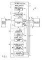
- FIG. 1 shows an entire configuration of a signal processing circuit 100 according to the present invention.
- a master device 1 is configured by a CPU
- a slave device 3 is configured by one or more memories such as SRAM.
- a case in which data is written in or read from the slave device 3 through a bus signal control circuit 2 according to the present invention will be described below.
- the configuration of the signal processing circuit 100 includes the master device 1 which controls transmission/reception of data, the slave device 3 which stores the data exchanged between the slave device 3 and the master device, and the bus signal control circuit 2 which controls a bus signal output to the slave device 3 according to an instruction from the master device 1.
- the bus signal control circuit 2 includes bus diagnosis lines 4, a memory control unit 21, an error address processing unit 22, and a bus signal abnormality processing unit 23.
- An address line and a control line which connect the bus signal control circuit 2 and the slave device 3 are connected to a receiving terminal 31 of the slave device 3.
- the bus diagnosis lines 4, as will be described later, are signal lines wired from the receiving terminal 31 to a feedback terminal 25 of the bus signal control circuit 2.
- a wire extending from the bus signal control circuit 2 to the feedback terminal 25 through the receiving terminal 31 is formed as a "single stroke continuous line".
- the memory control unit 21 controls data writing or data reading to the slave device 3 under the instruction of the master device 1.
- the bus signal abnormality processing unit 23 compares an output signal output from the bus signal control circuit 2 to an address line and a control line with a feedback signal fed back to the feedback terminal 25 through the bus diagnosis lines 4 to determine the presence/absence of a difference. When it is determined that the difference is present, the bus signal abnormality processing unit 23 generates a wait signal to elongate a bus cycle period of an operation being executed.
- the error address processing unit 22 includes an error address register 22a which temporarily stores error address data obtained at the time when a "difference-present signal" is output from the bus signal abnormality processing unit 23, and an address comparing unit 22b which compares the temporarily stored address with an address of an instruction to be executed next, to generate a signal for deleting, for example, the next instruction so that the error address data is not used.
- the memory control unit 21 includes a memory control circuit 21c which controls a bus signal (address signal and control signal) to write data in or read data from the slave device 3 according to an instruction from the master device 1; a reference clock signal generating circuit 21a which generates a reference clock signal Ck of a bus cycle in which the bus signal is transmitted; and a bus cycle period counter circuit 21b which generates a bus cycle signal TCkbc on the basis of the reference clock signal Ck.
- a memory control circuit 21c which controls a bus signal (address signal and control signal) to write data in or read data from the slave device 3 according to an instruction from the master device 1
- a reference clock signal generating circuit 21a which generates a reference clock signal Ck of a bus cycle in which the bus signal is transmitted
- a bus cycle period counter circuit 21b which generates a bus cycle signal TCkbc on the basis of the reference clock signal Ck.
- the bus signal abnormality processing unit 23 includes a bus signal comparing unit 23a which compares a bus signal output from the bus signal control circuit 2 to the address line and the control line with the feedback signal fed back to the feedback terminal 25 through the bus diagnosis lines 4 to detect the presence/absence of a difference; and a wait signal generating unit 23b which generates a wait signal to elongate a bus cycle period of an operation being executed when the bus signal comparing unit 23a outputs a signal representing the presence of the difference.
- the bus diagnosis lines 4 will be described below with reference to FIGS. 2A and 2B .
- the master device 1, the bus signal control circuit 2, and the slave device 3 may be mounted on one chip or different printed boards.
- the bus diagnosis lines 4 may be a pattern on a chip or wire lines between the circuit boards.
- each of the address line (address bus), the control line, and the data line (data bus) includes a large number of lines.
- the bus diagnosis lines 4 are signal lines extending from the receiving terminal 31 of the slave device 3 to the feedback terminal 25 of the bus signal control circuit 2.
- the address lines, the control lines, and the bus diagnosis lines 4 are arranged to extend from a transmitting terminal 24 to the feedback terminal 25 through the receiving terminal 31 as a single stroke continuous line. More specifically, the bus diagnosis lines 4 are directly connected to the receiving terminal 31 of the slave device 3 without passing through an address bus or a control signal line.
- Signal symbols shown in FIG. 2A denote symbols in a general-purpose SRAM.
- a signal transmitted through an address line is represented by Add*
- signals on a control line transmitted when data is written in or read from an SRAM are represented by CE1, CE2, R/W, OE, UB, and LB.
- the symbol added with a bar denotes a negative logic (active low) signal.
- the control signal R/W denotes a read signal or a write signal.
- an active (low level) output enable signal OE represents a read operation
- an inactive (high level) output enable signal represents a write operation.
- a signal transmitted from the bus signal control circuit 2 and a feedback signal fed back through the bus diagnosis lines 4 are discriminated from each other by adding FB to the head of the symbol of the feedback signal.
- a signal line extending from the transmitting terminal 24 to the receiving terminal 31 is represented by a solid line, and a feedback signal line for a signal returned to the feedback terminal 25 through the receiving terminal 31 is indicated by an alternate long and short dash line.
- the slave device 3 includes a plurality of memories 3a, 3b, and 3c as shown in FIG. 2B , the signal lines are arranged like a single stroke continuous line, and signal lines for a signal to be transmitted or received are arranged adjacent to each other, so that an external noise is prevented from being easily induced to the bus diagnosis lines 4.
- the transmitted signal and the fed back signal are compared with each other by the bus signal abnormality processing unit 23 on the transmission side to determine whether normal transmission is performed.
- FIG. 3A shows a time chart of a signal generated by the bus signal control circuit 2 according to the present invention.
- the bus cycle signal TCkbc indicates a transition of addresses and indicates 10 counts of the reference clock signal Ck as a bus cycle (one access period).
- This bus cycle is a bus cycle to an instruction signal O of the CPU serving as the master device 1, and is generated in the memory control unit 21.
- a preset address signal Address and a control signal (in this case, a chip enable signal CEa/CEb and a write or read signal R/W, UB, and LB) are generated depending on a value (value of a bus cycle BC) of the counter circuit 21b.
- the bus signal abnormality processing unit 23 when a difference between any corresponding bits of the transmitted bus signal (address signal in FIG. 3B ) and a fed back bus signal is detected, the bus signal abnormality processing unit 23 generates a wait signal Ws to notify the memory control unit 21 of the wait signal Ws.
- the memory control unit 21 elongates a bus cycle started at a detected timing by a period Tw.
- a dotted line of the read or write control signal R/W shown in FIG. 3B indicates a normal signal waveform obtained when no noise occurs.
- rising edge of the read or write control signal R/W is delayed by the period Tw with reference to normal rising edge. For example, in data writing, data on a data bus is written in a memory at rising edge of a write signal W.
- abnormality of a bus signal is detected on the basis of a difference between a transmitted signal and a signal received by the feedback terminal to elongate the bus cycle.
- elongation of the bus cycle even though an address error is caused by a noise, data is read or written at a timing at which an address is restored to a correct value.
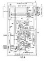
- the bus signal control circuit 2 will be described below in detail.
- the bus signal abnormality processing unit 23 will be described first with reference to FIGS. 4 to 7 , and the error address processing unit 22 will be described next with reference to FIG. 8 and FIGS. 9A and 9B .
- the bus signal abnormality processing unit 23 includes the bus signal comparing unit 23a, the wait signal generating unit 23b, and an I/O buffer 23c.
- the I/O buffer 23c converts feedback signals FB_Add*, FE_CE1, ... input through the bus diagnosis lines 4 into signals suitable for the circuits in the chip and outputs the signals as feedback signals FB_Address, FE_CEa, ....
- an electric level of a signal in a chip is different from an electric level of a signal outside the chip (voltage in the chip is lower), and high-active design may be conveniently adopted in the chip.
- the I/O buffer 23c performs such level conversion and logical conversion. In the embodiment, it is assumed that the logic of a signal in the chip is the same as that of a signal outside the chip.
- the bus signal comparing unit 23a compares the address signal Address and the control signals CEa ... transmitted from the memory control circuit 21c with the feedback address signals FB_Address and the feedback control signals FB_CEa ... received from the bus diagnosis lines 4 through the I/O buffer 23c, respectively, in correspondence with each other.
- the bus signal comparing unit 23a outputs the comparison results as Cosa and Cosb.
- the comparison result Cosa represents whether a difference between address signals is detected
- the comparison result Cosb represents whether a difference between control signals is detected.
- the wait signal generating unit 23b measures pulse widths of the comparison results Cosa and Cosb of the bus signal comparing unit 23a. When each of the pulse width is equal to or longer than a preset response time (sensitivity) of the slave device 3, the wait signal generating unit 23b outputs a "difference-present" signal.
- the bus signal comparing unit 23a includes a bus signal comparing unit A23a1 which detects an address error and a bus signal comparing unit B23a2 which detects an error of a control signal.
- the wait signal generating unit 23b includes a time measuring unit 23b1 which measures a pulse width of an output signal from the bus signal comparing unit A23a1, i.e., a difference-present signal (to be referred to as a mismatch pulse signal Cosa hereinafter) indicating an address error; a latch circuit 23b3 which latches the mismatch pulse signal Cosa; and a wait signal generating circuit A23b5 which receives an output signal Wma from the time measuring unit 23b1 and an output signal Loa from the latch circuit 23b3 to generate a wait signal Wsa.
- a time measuring unit 23b1 which measures a pulse width of an output signal from the bus signal comparing unit A23a1, i.e., a difference-present signal (to be referred to as a mismatch pulse signal Cosa hereinafter) indicating an address error
- a latch circuit 23b3 which latches the mismatch pulse signal Cosa
- a wait signal generating circuit A23b5 which receives an
- the wait signal generating unit 23b includes a time measuring unit 23b2 which measures a pulse width of an output signal from the bus signal comparing unit B23a2, i.e., a difference-present signal (to be referred to as a mismatch pulse signal Cosb hereinafter) indicating a control error; a latch circuit 23b4 which latch the mismatch pulse signal Cosb; and a wait signal generating circuit B23b6 which receives an output signal Wmb from the time measuring unit 23b2 and an output signal Lob from the latch circuit 23b4 to generate a wait signal Wsb.
- a time measuring unit 23b2 which measures a pulse width of an output signal from the bus signal comparing unit B23a2, i.e., a difference-present signal (to be referred to as a mismatch pulse signal Cosb hereinafter) indicating a control error
- a latch circuit 23b4 which latch the mismatch pulse signal Cosb
- a wait signal generating circuit B23b6 which receives an output signal W
- the wait signal generating unit 23b includes a wait signal synthesizing circuit 23b7 which synthesizes the wait signals Wsa and Wsb from the wait signal generating circuits 23b5 and 23b6 to generate a wait signal Ws.
- the transmitted address signal Address with the feedback address signal FB_Address are compared.
- the mismatch pulse signal Cosa is output. Therefore, as shown in FIG. 5B , when a noise is superposed on the address signal FB_Address (FB_Add*) of the bus diagnosis line 4, the mismatch pulse signal Cosa is output.
- a lower time chart in FIG. 5B shows a magnified operation in a period A immediately after the mismatch pulse signal Cosa is detected.
- the bus signal comparing unit A23a1 compares the address bus signal Address output from the memory control unit 21 with the address bus signal FB_Address fed back through the bus diagnosis line 4 bit by bit. When mismatch between any one pair of bits in the address bus signals configured by a plurality of bits is detected, the bus signal comparing unit A23a1 outputs the mismatch pulse signal Cosa.
- the feedback signal FB_Address is a signal obtained by simply feeding back the Address signal transmitted from the memory control unit 21 through the bus diagnosis line 4, the feedback signal FB_Address has basically the same logic as the signal Address. However, when the comparison result represents mismatch, it may be determined that a noise is mixed in any line of the address bus, and logical level thereof is changed.
- a time measuring unit A23b1 measures a pulse width of the mismatch pulse signal Cosa to determine whether the pulse width is a predetermined pulse width or more.
- the latch circuit 23b3 latches the mismatch pulse signal Cosa and outputs the signal as an output Loa.
- the outputs Wma and Loa from the time measuring unit A23b1 and the latch circuit 23b3 are reset at a start point of time (falling edge of the bus cycle signal TCkbc) of the bus cycle, and it is determined whether the mismatch pulse signal Cosa is detected in each bus cycle.
- the latch circuit 23b3 holds that the mismatch pulse signal Cosa is detected in the period of the bus cycle (output Loa).
- the time measuring unit A23b1 measures a time in which the mismatch pulse signal Cosa is generated. When the mismatch pulse signal Cosa continues for a predetermined time, i.e., sensitivity (a response time) or longer of the slave device 3, the time measuring unit A23b1 outputs the signal Wma.
- a clock signal Ckc to measure the pulse time is a signal having a frequency higher than that of the reference clock signal Ck.
- the wait signal generating circuit 23b5 outputs the wait signal Wsa (high-level signal) in a period of one cycle of the reference clock signal Ck when the bus cycle is a write cycle (W AB : Low) and the output Wma from the time measuring unit A23b1 is generated (Wma: High).
- the wait signal Wsa may be output.
- a pulse width of the mismatch pulse signal Cosa is measured.
- mismatch is desirably detected.
- the wait signal Wsa is input to the wait signal synthesizing circuit 23b7, and the wait signal Ws is transmitted from the wait signal synthesizing circuit 23b7 to the memory control circuit 21c.
- the memory control circuit 21c elongates the bus cycle by a period Tws in response to the wait signal Ws.
- the bus signal abnormality processing unit 23 can also perform error handling with the same configuration as described above even though a noise is superposed on the control signal.
- the bus signal abnormality processing unit 23 receives signals CEa (CE1), CEb (CE2), and Write which are control signals output to the slave device 3, signals FB_CEa (FB_CE1), FB_CEb (FB_CE2), and FB_Write (FB_R/W) fed back through the bus diagnosis lines 4, and the bus cycle signal TCkbc representing the start and the end of the bus cycle. Differences between the corresponding signals are detected by the bus signal comparing unit B23a2.
- FIG. 7 shows a case in which a noise is superposed on chip enable signals CE1 and CE2 in a write cycle.
- an error of the control signal is detected by the bus signal comparing unit B23a2, and the mismatch pulse signal Cosb is output.
- the output Wmb from the time measuring unit 23b2 which measures a pulse width of the mismatch pulse signal Cosb and the output Lob from the latch circuit 23b4 are input to the wait signal generating circuit B23b6.
- the wait signal Wsb is generated for a period of one cycle of the reference clock signal Ck.
- the wait signal Ws from the wait signal synthesizing circuit 23b7 is transmitted to the memory control circuit 21c, and the memory control circuit 21c elongates the bus cycle by a period Tws.
- an address signal transmitted from the memory control unit 21 is compared with an address signal fed back through the bus diagnosis line 4 to detect an address error, and the bus cycle is elongated. Therefore, a frequency of occurrence of an event in which data is written at an erroneous address or an event in which data is read from the erroneous address can be reduced.
- a frequency of execution of erroneous access caused by superposing a noise or the like on a control signal (chip select CE, read/write signal R/W, UB, or LU) can be reduced.
- a mismatch time of the address signal is measured.
- the mismatch time is equal to or shorter than a time in which the slave device 3 responds, the bus cycle can be avoided from being unnecessarily elongated because the time measuring unit which neglects the mismatch time is provided.
- the error address processing unit 22 includes a function of preventing erroneous data being latently present at the address from being read by the memory control unit 21 when the bus signal abnormality processing unit 23 detects an address error.
- the error address processing unit 22 includes the error address register 22a and the address comparing unit 22b which store a plurality of address data when a "difference-present" signal Cosa is generated at the bus signal abnormality processing unit 23.
- the address comparing unit 22b includes a comparing unit 22b1 and a processing unit 22b2.
- the comparing unit 22b1 compares address data "next Add" which will be accessed by the memory control unit 21 in the next bus cycle with address data EAdd stored in the error address register 22a and detected in this bus cycle.
- the processing unit 22b2 detects that a write instruction to the same address as the address EAdd is present in the next bus cycle, the processing unit 22b2 generates a clear signal RcI which clears the stored address data EAdd of the error address register 22a.
- the processing unit 22b2 detects that a read instruction which read data at the same address as the address EAdd is present, the processing unit 22b2 generates a "next read instruction Dse" signal which deletes the read signal.
- the wait signal generating unit 23b which generates a catch pulse signal CatchP to write data in the error address register 22a will be described below with reference to FIG. 4 .
- the wait signal generating unit 23b includes the wait signal generating circuit A23b5 which generates a catch pulse signal CatchP(a) from the address error and a wait signal generating circuit A23b6 which generates a catch pulse signal CatchP(b) from the control signal error.
- FIGS. 9A and 9B show a case in which a noise is detected in the address signal FB_Adress in a period near a rising edge of the write signal W and the write signal W rises before generation of the wait signal Wsa.
- data may be written at an erroneous address of the slave device (SRAM) 3.
- the wait signal generating circuit 23b5 receives, from the memory control unit 21, a read/write cycle signal R AB /W AB , the reference clock signal Ck, the output Wma from the time measuring unit 23b1, the output Loa from the latch circuit 23b3, and the mismatch pulse signal Cosa of the bus signal comparing unit A23a1.
- the read/write cycle signal R AB /W AB represents whether the bus cycle is a write cycle or a read cycle, and is a signal which does not change in one bus cycle.
- the mismatch pulse signal Cosa basically directly passes through the wait generating circuit A23b5 and is output as the signal CatchP(a).
- the bus signal comparing unit A23a1 detects mismatch between the address signal Address and the feedback address signal FB_Address, the bus signal comparing unit A23a1 outputs the mismatch signal Cosa. Since the signal FB_Address is a signal transmitted by the address bus including a plurality of signal lines, burst noises may be superposed on a plurality of address lines at slightly different timings. In this case, as shown in FIG. 9A , a plurality of mismatch pulse signals Cosa are generated. Therefore, the wait signal generating circuit 23b5, as shown in FIG. 9A , outputs a plurality of catch pulse signals CatchP(a).
- the FB_Address input to the bus signal comparing unit A23a1 is written in an error address register A22a in response to the signal CatchP(a).
- a plurality of catch pulse signals CatchP are output, a plurality of error addresses are stored in the error address register A22a.
- the error address register 22a includes a plurality of registers.
- the error address register 22a receives the signal FB_Address, the catch pulse signal CatchP(a), and the clear signal RcI and stores the value of the signal FB_Address at, for example, a rising edge of the catch pulse signal CatchP(a).
- the error address register 22a resets the contents of a designated register by the clear signal RcI as shown in the time chart in FIG. 9A .
- the address comparing unit 22b receives address data "next Add” used when the memory control unit 21 performs access in a next bus cycle n-1.
- the address comparing unit 22b receives a "next R AB /W AB signal" representing read access or write access performed by the memory control unit 21 in the next bus cycle and one or more error address values EAdd output from the error address register 22a.
- the address comparing unit 22b compares the "next Add" with one or more error address values EAdd. When the next Add is matched with any one of the error address values EAdd, and when the next access cycle is read access, the address comparing unit 22b outputs a next instruction read disable signal Dse as shown in the time chart in FIG. 9A to the memory control unit 21. When the next Add is matched with any one of the error address values, and when the next access cycle is write access, the address comparing unit 22b outputs the clear signal Rcl as shown in the time chart in FIG. 9A to the error address register 22a.
- the address comparing unit 22b resets (erases) corresponding error address information stored in the error address register 22a.
- the address comparing unit 22b When read access is performed to the same address as one of the plurality of addresses stored in the error address register 22a, the address comparing unit 22b notifies the memory control unit 21 that latent error data may be read.
- a host program, administrator, or the like
- an error address determining unit (not shown) which notifies the memory control unit 21 of that "next Add" having logic of bits close to logic of bits of the stored error address is suspicious, may be arranged.
- the slave device is not limited to an SRAM, and a DRAM which elongates a bus cycle may be used.
- a bus cycle may be used.
- optimum bus diagnosis lines are desirably arranged.
Landscapes
- Engineering & Computer Science (AREA)
- Theoretical Computer Science (AREA)
- General Engineering & Computer Science (AREA)
- Physics & Mathematics (AREA)
- General Physics & Mathematics (AREA)
- Quality & Reliability (AREA)
- Computer Hardware Design (AREA)
- Debugging And Monitoring (AREA)
- Techniques For Improving Reliability Of Storages (AREA)
- Bus Control (AREA)
Applications Claiming Priority (1)
| Application Number | Priority Date | Filing Date | Title |
|---|---|---|---|
| JP2008130475A JP5350677B2 (ja) | 2008-05-19 | 2008-05-19 | バス信号制御回路、及び、バス信号制御回路を備えた信号処理回路 |
Publications (2)
| Publication Number | Publication Date |
|---|---|
| EP2124154A1 true EP2124154A1 (de) | 2009-11-25 |
| EP2124154B1 EP2124154B1 (de) | 2012-09-05 |
Family
ID=40902723
Family Applications (1)
| Application Number | Title | Priority Date | Filing Date |
|---|---|---|---|
| EP09006017A Not-in-force EP2124154B1 (de) | 2008-05-19 | 2009-04-30 | Bussignal-Steuerschaltung und Signalverarbeitungsschaltung mit der Bussignal-Steuerschaltung |
Country Status (6)
| Country | Link |
|---|---|
| US (1) | US8131900B2 (de) |
| EP (1) | EP2124154B1 (de) |
| JP (1) | JP5350677B2 (de) |
| KR (1) | KR101067355B1 (de) |
| CN (1) | CN101587460B (de) |
| RU (1) | RU2421782C2 (de) |
Cited By (1)
| Publication number | Priority date | Publication date | Assignee | Title |
|---|---|---|---|---|
| EP2555123A1 (de) * | 2011-08-01 | 2013-02-06 | Hamilton Sundstrand Corporation | Bitübertragungsüberprüfung in einem ARINC-basierten System |
Families Citing this family (10)
| Publication number | Priority date | Publication date | Assignee | Title |
|---|---|---|---|---|
| CN103106142B (zh) * | 2011-11-10 | 2016-06-29 | 澜起科技(上海)有限公司 | 需要分配地址的器件、器件系统及地址分配方法 |
| CN102662782B (zh) | 2012-04-17 | 2014-09-03 | 华为技术有限公司 | 一种监控系统总线的方法及装置 |
| US9202041B2 (en) * | 2013-02-07 | 2015-12-01 | Fairchild Semiconductor Corporation | Permanent lockout attack detection |
| JP6263880B2 (ja) * | 2013-07-09 | 2018-01-24 | 富士通株式会社 | ストレージ制御装置、制御装置および制御プログラム |
| US9423820B2 (en) | 2013-07-31 | 2016-08-23 | Fairchild Semiconductor Corporation | Complimentary bit slicing side channel attack defense |
| JP6398390B2 (ja) * | 2014-07-03 | 2018-10-03 | 株式会社リコー | エラー検出方法及びエラー検出装置 |
| JP2017090963A (ja) * | 2015-11-02 | 2017-05-25 | 富士通株式会社 | 伝送装置及び故障診断方法 |
| JP6645467B2 (ja) * | 2017-03-28 | 2020-02-14 | 株式会社デンソー | マイクロコンピュータ |
| JP7031961B2 (ja) * | 2017-08-04 | 2022-03-08 | ソニーセミコンダクタソリューションズ株式会社 | 通信装置、通信方法、プログラム、および、通信システム |
| US11817169B2 (en) * | 2021-08-20 | 2023-11-14 | SK Hynix Inc. | Memory, memory system and operation method of memory system |
Citations (6)
| Publication number | Priority date | Publication date | Assignee | Title |
|---|---|---|---|---|
| US3555517A (en) * | 1968-10-30 | 1971-01-12 | Ibm | Early error detection system for data processing machine |
| JPH03238551A (ja) * | 1990-02-15 | 1991-10-24 | Aiphone Co Ltd | Cpu間のデータ伝送方式 |
| DE4212742A1 (de) * | 1992-04-16 | 1993-10-21 | Bayerische Motoren Werke Ag | Verfahren zur Fehlererkennung bei einem Datenbus |
| JPH1145214A (ja) | 1997-07-25 | 1999-02-16 | Sutetsupu One:Kk | エラー検出処理方法およびその装置 |
| JPH11167530A (ja) | 1997-12-04 | 1999-06-22 | Brother Ind Ltd | 信号制御回路 |
| JP2007148592A (ja) * | 2005-11-24 | 2007-06-14 | Funai Electric Co Ltd | データ通信装置 |
Family Cites Families (40)
| Publication number | Priority date | Publication date | Assignee | Title |
|---|---|---|---|---|
| JPS5837736B2 (ja) * | 1979-09-04 | 1983-08-18 | ファナック株式会社 | 直列デ−タ伝送方式 |
| US4845351A (en) * | 1985-09-30 | 1989-07-04 | Casio Computer Co., Ltd. | IC card |
| JP2538876B2 (ja) * | 1986-05-20 | 1996-10-02 | 富士通株式会社 | 共通バス構造を持つデ−タ処理装置 |
| SE454921B (sv) * | 1986-10-03 | 1988-06-06 | Ellemtel Utvecklings Ab | Sett och anordning for att i en pa forhand avgjord ordningsfoljd exekvera tva instuktionssekvenser |
| EP0306211A3 (de) * | 1987-09-04 | 1990-09-26 | Digital Equipment Corporation | Synchronisiertes Doppelrechnersystem |
| DE58901516D1 (de) | 1988-03-15 | 1992-07-02 | Siemens Ag | Verfahren zur datenuebertragung und anordnung zur durchfuehrung des verfahrens. |
| JPH0324601A (ja) | 1989-06-21 | 1991-02-01 | Japan Aviation Electron Ind Ltd | 制御方法 |
| JPH04105151A (ja) * | 1990-08-24 | 1992-04-07 | Nec Corp | 入出力制御装置 |
| CA2059143C (en) * | 1991-01-25 | 2000-05-16 | Takeshi Miyao | Processing unit for a computer and a computer system incorporating such a processing unit |
| JPH05324544A (ja) * | 1992-05-15 | 1993-12-07 | Hitachi Ltd | バス制御方法 |
| JP3256812B2 (ja) * | 1992-08-03 | 2002-02-18 | 株式会社日立製作所 | 通信制御装置およびプロセッサ装置 |
| US5590292A (en) * | 1992-12-08 | 1996-12-31 | Compaq Computer Corporation | Scalable tree structured high speed input/output subsystem architecture |
| GB2281137B (en) | 1993-08-20 | 1997-10-08 | Advanced Risc Mach Ltd | Data bus |
| JP3238551B2 (ja) | 1993-11-19 | 2001-12-17 | 沖電気工業株式会社 | 電界効果型トランジスタの製造方法 |
| CA2160500C (en) * | 1994-11-30 | 1999-11-09 | Amy Kulik | Pci/isa bridge having an arrangement for responding to pci bridge address parity errors for internal pci slaves in the pci/isa bridge |
| JPH11242638A (ja) | 1998-02-24 | 1999-09-07 | Ando Electric Co Ltd | データ処理システム |
| JP3540243B2 (ja) * | 2000-04-24 | 2004-07-07 | Necエレクトロニクス株式会社 | 半導体記憶装置 |
| US6772388B2 (en) * | 2000-12-06 | 2004-08-03 | Motorola, Inc | Apparatus and method for providing optimal adaptive forward error correction in data communications |
| US20020091976A1 (en) * | 2001-01-09 | 2002-07-11 | Lee Whay Sing | Reverse parity coding |
| KR20020071297A (ko) | 2001-03-06 | 2002-09-12 | 삼성전자 주식회사 | 시스템의 버스 정합 검증 장치 및 방법 |
| JP4071464B2 (ja) * | 2001-07-17 | 2008-04-02 | 株式会社東芝 | 音声クロック復元装置及び音声クロック復元方法 |
| EP1376356A1 (de) * | 2002-06-26 | 2004-01-02 | Fujitsu Siemens Computers, LLC | Fehlerrapportierungsnetzwerk in einem mehrrechnersystem |
| US7386639B2 (en) * | 2003-01-15 | 2008-06-10 | Avago Technologies Fiber Ip (Singapore) Pte. Ltd. | Switch for coupling one bus to another bus |
| US7234099B2 (en) * | 2003-04-14 | 2007-06-19 | International Business Machines Corporation | High reliability memory module with a fault tolerant address and command bus |
| US20040237001A1 (en) * | 2003-05-21 | 2004-11-25 | Sun Microsystems, Inc. | Memory integrated circuit including an error detection mechanism for detecting errors in address and control signals |
| US7577756B2 (en) * | 2003-07-15 | 2009-08-18 | Special Devices, Inc. | Dynamically-and continuously-variable rate, asynchronous data transfer |
| JP2005086683A (ja) * | 2003-09-10 | 2005-03-31 | Fanuc Ltd | 誤り復号回路、データバス制御方法、及びデータバスシステム |
| US7386765B2 (en) * | 2003-09-29 | 2008-06-10 | Intel Corporation | Memory device having error checking and correction |
| EP1640850A1 (de) * | 2004-09-27 | 2006-03-29 | STMicroelectronics S.r.l. | Steuerschaltung für einen gemeinsamen Bus für Signal Regler |
| US7330050B2 (en) * | 2004-11-08 | 2008-02-12 | Tabula, Inc. | Storage elements for a configurable IC and method and apparatus for accessing data stored in the storage elements |
| US7268586B1 (en) * | 2004-11-08 | 2007-09-11 | Tabula, Inc. | Method and apparatus for accessing stored data in a reconfigurable IC |
| US7224181B1 (en) * | 2004-11-08 | 2007-05-29 | Herman Schmit | Clock distribution in a configurable IC |
| US7475304B1 (en) * | 2005-02-25 | 2009-01-06 | The United States Of America As Represented By The Secretary Of The Air Force | Bit error tester |
| RU2295748C2 (ru) | 2005-05-26 | 2007-03-20 | Федеральное государственное унитарное предприятие "Научно-производственное объединение автоматики" им. акад. Н.А. Семихатова | Устройство ввода-вывода |
| DE102005053103B4 (de) * | 2005-11-04 | 2008-04-24 | Phoenix Contact Gmbh & Co. Kg | Verfahren sowie System zur Übertragung von zyklischen und azyklischen Daten |
| JP4186168B2 (ja) * | 2006-06-06 | 2008-11-26 | 村田機械株式会社 | ファイル送信端末 |
| CA2592908A1 (en) * | 2006-06-30 | 2007-12-30 | Hitachi, Ltd. | Line diagnostic device, bus system, line diagnostic method, bus system control method, and line diagnostic program |
| US8086357B2 (en) * | 2006-09-22 | 2011-12-27 | Siemens Industry, Inc. | Offline configuration using USB download in an integrated power distribution system |
| US8018089B2 (en) * | 2006-09-22 | 2011-09-13 | Siemens Industry, Inc. | System controller for integrated lighting control panels |
| US8347165B2 (en) * | 2007-12-17 | 2013-01-01 | Micron Technology, Inc. | Self-timed error correcting code evaluation system and method |
-
2008
- 2008-05-19 JP JP2008130475A patent/JP5350677B2/ja not_active Expired - Fee Related
-
2009
- 2009-04-30 EP EP09006017A patent/EP2124154B1/de not_active Not-in-force
- 2009-04-30 US US12/432,896 patent/US8131900B2/en not_active Expired - Fee Related
- 2009-05-18 KR KR1020090043229A patent/KR101067355B1/ko not_active Expired - Fee Related
- 2009-05-18 RU RU2009118689/08A patent/RU2421782C2/ru active
- 2009-05-19 CN CN2009102036153A patent/CN101587460B/zh not_active Expired - Fee Related
Patent Citations (6)
| Publication number | Priority date | Publication date | Assignee | Title |
|---|---|---|---|---|
| US3555517A (en) * | 1968-10-30 | 1971-01-12 | Ibm | Early error detection system for data processing machine |
| JPH03238551A (ja) * | 1990-02-15 | 1991-10-24 | Aiphone Co Ltd | Cpu間のデータ伝送方式 |
| DE4212742A1 (de) * | 1992-04-16 | 1993-10-21 | Bayerische Motoren Werke Ag | Verfahren zur Fehlererkennung bei einem Datenbus |
| JPH1145214A (ja) | 1997-07-25 | 1999-02-16 | Sutetsupu One:Kk | エラー検出処理方法およびその装置 |
| JPH11167530A (ja) | 1997-12-04 | 1999-06-22 | Brother Ind Ltd | 信号制御回路 |
| JP2007148592A (ja) * | 2005-11-24 | 2007-06-14 | Funai Electric Co Ltd | データ通信装置 |
Cited By (2)
| Publication number | Priority date | Publication date | Assignee | Title |
|---|---|---|---|---|
| EP2555123A1 (de) * | 2011-08-01 | 2013-02-06 | Hamilton Sundstrand Corporation | Bitübertragungsüberprüfung in einem ARINC-basierten System |
| US8467914B2 (en) | 2011-08-01 | 2013-06-18 | Hamilton Sunstrand Corporation | Bit transmission verification in an ARINC-based system |
Also Published As
| Publication number | Publication date |
|---|---|
| JP5350677B2 (ja) | 2013-11-27 |
| EP2124154B1 (de) | 2012-09-05 |
| KR101067355B1 (ko) | 2011-09-23 |
| KR20090120415A (ko) | 2009-11-24 |
| RU2421782C2 (ru) | 2011-06-20 |
| JP2009277174A (ja) | 2009-11-26 |
| US20090287867A1 (en) | 2009-11-19 |
| RU2009118689A (ru) | 2010-11-27 |
| US8131900B2 (en) | 2012-03-06 |
| CN101587460B (zh) | 2011-11-23 |
| CN101587460A (zh) | 2009-11-25 |
Similar Documents
| Publication | Publication Date | Title |
|---|---|---|
| EP2124154B1 (de) | Bussignal-Steuerschaltung und Signalverarbeitungsschaltung mit der Bussignal-Steuerschaltung | |
| US11568917B1 (en) | Hammer refresh row address detector, and semiconductor memory device and memory module including the same | |
| AU2017377949B2 (en) | Clock gating enable generation | |
| US9110796B2 (en) | Apparatus and circuitry for memory-based collection and verification of data integrity information | |
| JP2005149501A (ja) | Dmaを使用して拡張カードでメモリをテストするためのシステムおよび方法 | |
| JP5006121B2 (ja) | 論理検証装置、論理検証方法 | |
| US8775745B2 (en) | Process variation tolerant bank collision detection circuit | |
| JP2010040092A (ja) | 半導体集積回路 | |
| JPH06309185A (ja) | 情報処理装置 | |
| KR100668676B1 (ko) | 기지국 보드 장애 검출 및 상태 변화 감지 장치 및 방법 | |
| JP2018156188A (ja) | メモリ制御装置、情報処理装置およびメモリ制御方法 | |
| JP5529794B2 (ja) | マイクロコンピュータ及び異常メモリアクセス検出方法 | |
| JP2536781B2 (ja) | パリティチェック装置 | |
| US8245121B2 (en) | Signal control circuit and signal control apparatus | |
| JPS6252649A (ja) | メモリ素子用ハ−ドエラ−検出装置 | |
| JP2000293278A (ja) | ノイズ検出回路 | |
| JPH0520131A (ja) | アドレス監視方式 | |
| JP2012146167A (ja) | メモリエラーパターン記録システム、メモリモジュール、及びメモリエラーパターン記録方法 | |
| JPH0675825A (ja) | コンピュータシステム | |
| JPH0644098A (ja) | メモリ・アクセス・バス・コンパレータ | |
| JPS5816556B2 (ja) | エラ−検出方式 | |
| JPH05165658A (ja) | 情報処理システム | |
| JPH01258054A (ja) | 記憶装置のアクセス制御方式 | |
| JPH04287253A (ja) | パリティ検査回路 | |
| JP2010198098A (ja) | 情報処理装置、バス制御回路、バス制御方法及びバス制御プログラム |
Legal Events
| Date | Code | Title | Description |
|---|---|---|---|
| PUAI | Public reference made under article 153(3) epc to a published international application that has entered the european phase |
Free format text: ORIGINAL CODE: 0009012 |
|
| 17P | Request for examination filed |
Effective date: 20090430 |
|
| AK | Designated contracting states |
Kind code of ref document: A1 Designated state(s): AT BE BG CH CY CZ DE DK EE ES FI FR GB GR HR HU IE IS IT LI LT LU LV MC MK MT NL NO PL PT RO SE SI SK TR |
|
| 17Q | First examination report despatched |
Effective date: 20100111 |
|
| GRAP | Despatch of communication of intention to grant a patent |
Free format text: ORIGINAL CODE: EPIDOSNIGR1 |
|
| GRAS | Grant fee paid |
Free format text: ORIGINAL CODE: EPIDOSNIGR3 |
|
| GRAA | (expected) grant |
Free format text: ORIGINAL CODE: 0009210 |
|
| AK | Designated contracting states |
Kind code of ref document: B1 Designated state(s): AT BE BG CH CY CZ DE DK EE ES FI FR GB GR HR HU IE IS IT LI LT LU LV MC MK MT NL NO PL PT RO SE SI SK TR |
|
| REG | Reference to a national code |
Ref country code: GB Ref legal event code: FG4D |
|
| REG | Reference to a national code |
Ref country code: CH Ref legal event code: EP |
|
| REG | Reference to a national code |
Ref country code: AT Ref legal event code: REF Ref document number: 574392 Country of ref document: AT Kind code of ref document: T Effective date: 20120915 |
|
| REG | Reference to a national code |
Ref country code: IE Ref legal event code: FG4D |
|
| REG | Reference to a national code |
Ref country code: DE Ref legal event code: R096 Ref document number: 602009009394 Country of ref document: DE Effective date: 20121031 |
|
| REG | Reference to a national code |
Ref country code: AT Ref legal event code: MK05 Ref document number: 574392 Country of ref document: AT Kind code of ref document: T Effective date: 20120905 |
|
| REG | Reference to a national code |
Ref country code: NL Ref legal event code: VDEP Effective date: 20120905 |
|
| PG25 | Lapsed in a contracting state [announced via postgrant information from national office to epo] |
Ref country code: CY Free format text: LAPSE BECAUSE OF FAILURE TO SUBMIT A TRANSLATION OF THE DESCRIPTION OR TO PAY THE FEE WITHIN THE PRESCRIBED TIME-LIMIT Effective date: 20120905 Ref country code: AT Free format text: LAPSE BECAUSE OF FAILURE TO SUBMIT A TRANSLATION OF THE DESCRIPTION OR TO PAY THE FEE WITHIN THE PRESCRIBED TIME-LIMIT Effective date: 20120905 Ref country code: LT Free format text: LAPSE BECAUSE OF FAILURE TO SUBMIT A TRANSLATION OF THE DESCRIPTION OR TO PAY THE FEE WITHIN THE PRESCRIBED TIME-LIMIT Effective date: 20120905 Ref country code: FI Free format text: LAPSE BECAUSE OF FAILURE TO SUBMIT A TRANSLATION OF THE DESCRIPTION OR TO PAY THE FEE WITHIN THE PRESCRIBED TIME-LIMIT Effective date: 20120905 Ref country code: HR Free format text: LAPSE BECAUSE OF FAILURE TO SUBMIT A TRANSLATION OF THE DESCRIPTION OR TO PAY THE FEE WITHIN THE PRESCRIBED TIME-LIMIT Effective date: 20120905 Ref country code: NO Free format text: LAPSE BECAUSE OF FAILURE TO SUBMIT A TRANSLATION OF THE DESCRIPTION OR TO PAY THE FEE WITHIN THE PRESCRIBED TIME-LIMIT Effective date: 20121205 |
|
| REG | Reference to a national code |
Ref country code: LT Ref legal event code: MG4D Effective date: 20120905 |
|
| PG25 | Lapsed in a contracting state [announced via postgrant information from national office to epo] |
Ref country code: LV Free format text: LAPSE BECAUSE OF FAILURE TO SUBMIT A TRANSLATION OF THE DESCRIPTION OR TO PAY THE FEE WITHIN THE PRESCRIBED TIME-LIMIT Effective date: 20120905 Ref country code: SE Free format text: LAPSE BECAUSE OF FAILURE TO SUBMIT A TRANSLATION OF THE DESCRIPTION OR TO PAY THE FEE WITHIN THE PRESCRIBED TIME-LIMIT Effective date: 20120905 Ref country code: SI Free format text: LAPSE BECAUSE OF FAILURE TO SUBMIT A TRANSLATION OF THE DESCRIPTION OR TO PAY THE FEE WITHIN THE PRESCRIBED TIME-LIMIT Effective date: 20120905 Ref country code: GR Free format text: LAPSE BECAUSE OF FAILURE TO SUBMIT A TRANSLATION OF THE DESCRIPTION OR TO PAY THE FEE WITHIN THE PRESCRIBED TIME-LIMIT Effective date: 20121206 |
|
| PG25 | Lapsed in a contracting state [announced via postgrant information from national office to epo] |
Ref country code: NL Free format text: LAPSE BECAUSE OF FAILURE TO SUBMIT A TRANSLATION OF THE DESCRIPTION OR TO PAY THE FEE WITHIN THE PRESCRIBED TIME-LIMIT Effective date: 20120905 Ref country code: EE Free format text: LAPSE BECAUSE OF FAILURE TO SUBMIT A TRANSLATION OF THE DESCRIPTION OR TO PAY THE FEE WITHIN THE PRESCRIBED TIME-LIMIT Effective date: 20120905 Ref country code: BE Free format text: LAPSE BECAUSE OF FAILURE TO SUBMIT A TRANSLATION OF THE DESCRIPTION OR TO PAY THE FEE WITHIN THE PRESCRIBED TIME-LIMIT Effective date: 20120905 Ref country code: CZ Free format text: LAPSE BECAUSE OF FAILURE TO SUBMIT A TRANSLATION OF THE DESCRIPTION OR TO PAY THE FEE WITHIN THE PRESCRIBED TIME-LIMIT Effective date: 20120905 Ref country code: IS Free format text: LAPSE BECAUSE OF FAILURE TO SUBMIT A TRANSLATION OF THE DESCRIPTION OR TO PAY THE FEE WITHIN THE PRESCRIBED TIME-LIMIT Effective date: 20130105 Ref country code: RO Free format text: LAPSE BECAUSE OF FAILURE TO SUBMIT A TRANSLATION OF THE DESCRIPTION OR TO PAY THE FEE WITHIN THE PRESCRIBED TIME-LIMIT Effective date: 20120905 Ref country code: ES Free format text: LAPSE BECAUSE OF FAILURE TO SUBMIT A TRANSLATION OF THE DESCRIPTION OR TO PAY THE FEE WITHIN THE PRESCRIBED TIME-LIMIT Effective date: 20121216 |
|
| PG25 | Lapsed in a contracting state [announced via postgrant information from national office to epo] |
Ref country code: PT Free format text: LAPSE BECAUSE OF FAILURE TO SUBMIT A TRANSLATION OF THE DESCRIPTION OR TO PAY THE FEE WITHIN THE PRESCRIBED TIME-LIMIT Effective date: 20130107 Ref country code: PL Free format text: LAPSE BECAUSE OF FAILURE TO SUBMIT A TRANSLATION OF THE DESCRIPTION OR TO PAY THE FEE WITHIN THE PRESCRIBED TIME-LIMIT Effective date: 20120905 Ref country code: SK Free format text: LAPSE BECAUSE OF FAILURE TO SUBMIT A TRANSLATION OF THE DESCRIPTION OR TO PAY THE FEE WITHIN THE PRESCRIBED TIME-LIMIT Effective date: 20120905 |
|
| PLBE | No opposition filed within time limit |
Free format text: ORIGINAL CODE: 0009261 |
|
| STAA | Information on the status of an ep patent application or granted ep patent |
Free format text: STATUS: NO OPPOSITION FILED WITHIN TIME LIMIT |
|
| PG25 | Lapsed in a contracting state [announced via postgrant information from national office to epo] |
Ref country code: BG Free format text: LAPSE BECAUSE OF FAILURE TO SUBMIT A TRANSLATION OF THE DESCRIPTION OR TO PAY THE FEE WITHIN THE PRESCRIBED TIME-LIMIT Effective date: 20121205 Ref country code: DK Free format text: LAPSE BECAUSE OF FAILURE TO SUBMIT A TRANSLATION OF THE DESCRIPTION OR TO PAY THE FEE WITHIN THE PRESCRIBED TIME-LIMIT Effective date: 20120905 |
|
| 26N | No opposition filed |
Effective date: 20130606 |
|
| REG | Reference to a national code |
Ref country code: DE Ref legal event code: R097 Ref document number: 602009009394 Country of ref document: DE Effective date: 20130606 |
|
| PG25 | Lapsed in a contracting state [announced via postgrant information from national office to epo] |
Ref country code: MC Free format text: LAPSE BECAUSE OF FAILURE TO SUBMIT A TRANSLATION OF THE DESCRIPTION OR TO PAY THE FEE WITHIN THE PRESCRIBED TIME-LIMIT Effective date: 20120905 |
|
| REG | Reference to a national code |
Ref country code: CH Ref legal event code: PL |
|
| REG | Reference to a national code |
Ref country code: IE Ref legal event code: MM4A |
|
| PG25 | Lapsed in a contracting state [announced via postgrant information from national office to epo] |
Ref country code: LI Free format text: LAPSE BECAUSE OF NON-PAYMENT OF DUE FEES Effective date: 20130430 Ref country code: CH Free format text: LAPSE BECAUSE OF NON-PAYMENT OF DUE FEES Effective date: 20130430 |
|
| PG25 | Lapsed in a contracting state [announced via postgrant information from national office to epo] |
Ref country code: IE Free format text: LAPSE BECAUSE OF NON-PAYMENT OF DUE FEES Effective date: 20130430 |
|
| PG25 | Lapsed in a contracting state [announced via postgrant information from national office to epo] |
Ref country code: MT Free format text: LAPSE BECAUSE OF FAILURE TO SUBMIT A TRANSLATION OF THE DESCRIPTION OR TO PAY THE FEE WITHIN THE PRESCRIBED TIME-LIMIT Effective date: 20120905 |
|
| PG25 | Lapsed in a contracting state [announced via postgrant information from national office to epo] |
Ref country code: TR Free format text: LAPSE BECAUSE OF FAILURE TO SUBMIT A TRANSLATION OF THE DESCRIPTION OR TO PAY THE FEE WITHIN THE PRESCRIBED TIME-LIMIT Effective date: 20120905 |
|
| PG25 | Lapsed in a contracting state [announced via postgrant information from national office to epo] |
Ref country code: LU Free format text: LAPSE BECAUSE OF NON-PAYMENT OF DUE FEES Effective date: 20130430 Ref country code: HU Free format text: LAPSE BECAUSE OF FAILURE TO SUBMIT A TRANSLATION OF THE DESCRIPTION OR TO PAY THE FEE WITHIN THE PRESCRIBED TIME-LIMIT; INVALID AB INITIO Effective date: 20090430 Ref country code: MK Free format text: LAPSE BECAUSE OF FAILURE TO SUBMIT A TRANSLATION OF THE DESCRIPTION OR TO PAY THE FEE WITHIN THE PRESCRIBED TIME-LIMIT Effective date: 20120905 |
|
| REG | Reference to a national code |
Ref country code: FR Ref legal event code: PLFP Year of fee payment: 8 |
|
| REG | Reference to a national code |
Ref country code: FR Ref legal event code: PLFP Year of fee payment: 9 |
|
| REG | Reference to a national code |
Ref country code: FR Ref legal event code: PLFP Year of fee payment: 10 |
|
| PGFP | Annual fee paid to national office [announced via postgrant information from national office to epo] |
Ref country code: IT Payment date: 20190419 Year of fee payment: 11 Ref country code: DE Payment date: 20190416 Year of fee payment: 11 |
|
| PGFP | Annual fee paid to national office [announced via postgrant information from national office to epo] |
Ref country code: GB Payment date: 20190424 Year of fee payment: 11 |
|
| REG | Reference to a national code |
Ref country code: DE Ref legal event code: R119 Ref document number: 602009009394 Country of ref document: DE |
|
| PG25 | Lapsed in a contracting state [announced via postgrant information from national office to epo] |
Ref country code: DE Free format text: LAPSE BECAUSE OF NON-PAYMENT OF DUE FEES Effective date: 20201103 |
|
| GBPC | Gb: european patent ceased through non-payment of renewal fee |
Effective date: 20200430 |
|
| PG25 | Lapsed in a contracting state [announced via postgrant information from national office to epo] |
Ref country code: GB Free format text: LAPSE BECAUSE OF NON-PAYMENT OF DUE FEES Effective date: 20200430 |
|
| PGFP | Annual fee paid to national office [announced via postgrant information from national office to epo] |
Ref country code: FR Payment date: 20210309 Year of fee payment: 13 |
|
| PG25 | Lapsed in a contracting state [announced via postgrant information from national office to epo] |
Ref country code: IT Free format text: LAPSE BECAUSE OF NON-PAYMENT OF DUE FEES Effective date: 20200430 |
|
| PG25 | Lapsed in a contracting state [announced via postgrant information from national office to epo] |
Ref country code: FR Free format text: LAPSE BECAUSE OF NON-PAYMENT OF DUE FEES Effective date: 20220430 |