EP2073270B1 - Solid-state imaging device and camera - Google Patents
Solid-state imaging device and camera Download PDFInfo
- Publication number
- EP2073270B1 EP2073270B1 EP08021947.0A EP08021947A EP2073270B1 EP 2073270 B1 EP2073270 B1 EP 2073270B1 EP 08021947 A EP08021947 A EP 08021947A EP 2073270 B1 EP2073270 B1 EP 2073270B1
- Authority
- EP
- European Patent Office
- Prior art keywords
- well
- imaging device
- solid
- conductive
- state imaging
- Prior art date
- Legal status (The legal status is an assumption and is not a legal conclusion. Google has not performed a legal analysis and makes no representation as to the accuracy of the status listed.)
- Not-in-force
Links
Images


Classifications
-
- H—ELECTRICITY
- H10—SEMICONDUCTOR DEVICES; ELECTRIC SOLID-STATE DEVICES NOT OTHERWISE PROVIDED FOR
- H10F—INORGANIC SEMICONDUCTOR DEVICES SENSITIVE TO INFRARED RADIATION, LIGHT, ELECTROMAGNETIC RADIATION OF SHORTER WAVELENGTH OR CORPUSCULAR RADIATION
- H10F39/00—Integrated devices, or assemblies of multiple devices, comprising at least one element covered by group H10F30/00, e.g. radiation detectors comprising photodiode arrays
- H10F39/10—Integrated devices
- H10F39/12—Image sensors
- H10F39/199—Back-illuminated image sensors
-
- H—ELECTRICITY
- H10—SEMICONDUCTOR DEVICES; ELECTRIC SOLID-STATE DEVICES NOT OTHERWISE PROVIDED FOR
- H10F—INORGANIC SEMICONDUCTOR DEVICES SENSITIVE TO INFRARED RADIATION, LIGHT, ELECTROMAGNETIC RADIATION OF SHORTER WAVELENGTH OR CORPUSCULAR RADIATION
- H10F39/00—Integrated devices, or assemblies of multiple devices, comprising at least one element covered by group H10F30/00, e.g. radiation detectors comprising photodiode arrays
- H10F39/80—Constructional details of image sensors
- H10F39/805—Coatings
- H10F39/8053—Colour filters
-
- H—ELECTRICITY
- H10—SEMICONDUCTOR DEVICES; ELECTRIC SOLID-STATE DEVICES NOT OTHERWISE PROVIDED FOR
- H10F—INORGANIC SEMICONDUCTOR DEVICES SENSITIVE TO INFRARED RADIATION, LIGHT, ELECTROMAGNETIC RADIATION OF SHORTER WAVELENGTH OR CORPUSCULAR RADIATION
- H10F39/00—Integrated devices, or assemblies of multiple devices, comprising at least one element covered by group H10F30/00, e.g. radiation detectors comprising photodiode arrays
- H10F39/80—Constructional details of image sensors
- H10F39/805—Coatings
- H10F39/8057—Optical shielding
-
- H—ELECTRICITY
- H10—SEMICONDUCTOR DEVICES; ELECTRIC SOLID-STATE DEVICES NOT OTHERWISE PROVIDED FOR
- H10F—INORGANIC SEMICONDUCTOR DEVICES SENSITIVE TO INFRARED RADIATION, LIGHT, ELECTROMAGNETIC RADIATION OF SHORTER WAVELENGTH OR CORPUSCULAR RADIATION
- H10F39/00—Integrated devices, or assemblies of multiple devices, comprising at least one element covered by group H10F30/00, e.g. radiation detectors comprising photodiode arrays
- H10F39/80—Constructional details of image sensors
- H10F39/806—Optical elements or arrangements associated with the image sensors
- H10F39/8063—Microlenses
-
- H—ELECTRICITY
- H10—SEMICONDUCTOR DEVICES; ELECTRIC SOLID-STATE DEVICES NOT OTHERWISE PROVIDED FOR
- H10F—INORGANIC SEMICONDUCTOR DEVICES SENSITIVE TO INFRARED RADIATION, LIGHT, ELECTROMAGNETIC RADIATION OF SHORTER WAVELENGTH OR CORPUSCULAR RADIATION
- H10F39/00—Integrated devices, or assemblies of multiple devices, comprising at least one element covered by group H10F30/00, e.g. radiation detectors comprising photodiode arrays
- H10F39/80—Constructional details of image sensors
- H10F39/806—Optical elements or arrangements associated with the image sensors
- H10F39/8067—Reflectors
-
- H—ELECTRICITY
- H10—SEMICONDUCTOR DEVICES; ELECTRIC SOLID-STATE DEVICES NOT OTHERWISE PROVIDED FOR
- H10F—INORGANIC SEMICONDUCTOR DEVICES SENSITIVE TO INFRARED RADIATION, LIGHT, ELECTROMAGNETIC RADIATION OF SHORTER WAVELENGTH OR CORPUSCULAR RADIATION
- H10F39/00—Integrated devices, or assemblies of multiple devices, comprising at least one element covered by group H10F30/00, e.g. radiation detectors comprising photodiode arrays
- H10F39/80—Constructional details of image sensors
- H10F39/807—Pixel isolation structures
Definitions
- the present invention relates to a solid-state imaging device and a camera having a photoelectric conversion element.
- an embedded photodiode structure As a method of suppressing the occurrence of the dark currents due to the interface state density, an embedded photodiode structure is effective.
- the embedded photodiode is configured by, for example, forming an n-type semiconductor region and forming a shallow p-type semiconductor region (a hole accumulation region) with high impurity density for the suppression of the dark currents near the surface of the n-type semiconductor region, i.e., an interface between the n-type semiconductor region and an insulating film.
- the embedded photodiode As a method of manufacturing the embedded photodiode, it is a general practice to ion-implant B or BF 2 serving as p-type impurities and annealing the same and form a p-type semiconductor region near the interface between the n-type semiconductor region forming the photodiode and the insulating film.
- each of pixels includes a photodiode and various kinds of transistors such as readout, reset, and amplification transistors.
- a signal photoelectrically converted by the photodiode is processed by these transistors.
- a wiring layer including multi-layer metal wiring is formed above each of the pixels.
- a color filter that specifies the wavelength of light made incident on the photodiode and an on-chip lens that condenses light on the photodiode are formed on the wiring layer.
- CMOS image sensor As such a CMOS image sensor, device structures having various characteristics are proposed.
- CCD charge modulation device
- BCMD bulk charge modulation device
- FWA floating well amplifier
- VMIS Vth modulation image sensor
- a solid-state imaging device in which a light sensing element having all functions of performing photoelectric conversion using incident light, accumulating signal charges obtained by the photoelectric conversion, and outputting signal voltage according to a charge amount of the accumulated signal charges has a potential distribution for facilitating the signal charges to be accumulated in the same place in terms of a plane and facilitating a surface channel current to flow (see JP-A-2003-31785 ).
- CMOS image sensors are basically front-illuminated solid-state imaging devices that irradiate light from a front side of a device.
- a back (rear)-illuminated solid-state imaging device that has a rear side of a silicon substrate, on which a photodiode and various transistors are formed, ground to be thinned and makes light incident from the rear side of the substrate to perform photoelectric conversion (see JP-A-10-65138 ).
- a current-voltage characteristic (ID-VDD) is not a saturation characteristic but is a triode characteristic. Therefore, there is a disadvantage that, when the image sensor is used in a source follower type, the image sensor is hard to use.
- CMOS image sensor there is a disadvantage that light is blocked by wiring above pixels, sensitivity of each of the pixels falls, and, when the light reflected by the wiring is made incident on adjacent pixels, color mixture and the like are caused.
- this solid-state imaging device is also the front-illuminated type, the solid-state imaging device also has the problems such as the fall in the blue sensitivity and the color mixture of the front-illuminated type.
- a solid-state imaging device and a camera that can efficiently and quickly perform a series of operations such as generation and accumulation of photo-carriers, readout of charges, and transmission (reset) of remaining charges, prevent the influence of a trap on carriers in a silicon interface due to light, and realize improvement of sensitivity and pixel size shrinking without deteriorating sensitivity of light with respect to blue.
- light is irradiated on the pixels of the cell structure from the substrate rear surface (first substrate surface) side, photoelectric conversion of the received light is performed in the first conductive well, and charges of the light is accumulated.
- the charge accumulation is detected and threshold modulation of the transistor formed in the second conductive well is performed to extract a signal.
- the pixel cells have the double-well structure in the back-illuminated type.
- the accumulated charges and channel currents are identical carriers.
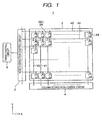
- Fig. 1 is a block diagram of a schematic configuration of a solid-state imaging device according to an embodiment of the present invention.
- a solid-state imaging device 1 includes, as shown in Fig. 1 , a pixel section 2 as a sensing section, a row direction (Y-direction) control circuit 3, a column direction (X direction) control circuit 4, and a timing control circuit 5.
- plural pixel cells 2A are arranged in, for example, a matrix shape.
- the pixel cells 2A of the pixel section 2 is configured as a rear (back)-illuminated image sensor of a threshold modulation (CMD) system having the double-well structure.
- CMD threshold modulation
- the pixel section 2 adopts the double-well structure.
- accumulated charges and channel currents are identical carriers.
- the pixel section 2 has a one-transistor architecture (structure) in which one transistor has functions of a readout transistor, a reset transistor, and a selection transistor.
- the pixel cells 2A arranged in an identical row are connected to common row lines H0, H1, and the like and the pixel cells 2A arranged in an identical column are connected to common column lines V0, V1, and the like.
- a timing control circuit 5 that generates an internal clock
- a row direction (Y direction) control circuit 3 that controls a row address and row scanning
- a column direction (X direction) control circuit 4 that controls a column address and column scanning are arranged as control circuits for sequentially reading out signals of the pixel section 2.
- the row direction (Y direction) control circuit 3 receives a timing control pulse of the timing control circuit 5 and drives predetermined row lines H0, H1, and the like.
- the row direction (X direction) control circuit 4 receives timing control pulse of the timing control circuit 5, receives signals read out to predetermined column lines V0, V1, and the like, and performs predetermined processing (CDS (Correlated Double Sampling) processing), analog to digital conversion processing, and the like.
- CDS Correlated Double Sampling
- Figs. 2A and 2B are diagrams of a basic structure of the pixel section of the solid-state imaging device according to this embodiment.
- Fig. 2A is a plan view and Fig. 2B is a simplified sectional view taken along an a-a' line shown in Fig. 2A .
- the solid-state imaging device 1 is formed as a rear (back)-illuminated device in which light is made incident from a first substrate surface 101 side (a rear side) of a substrate (a silicon substrate) 100 and an element area portion EAP, in which a MOS transistor is formed, is formed on a second substrate surface 102 side (a front side).
- the substrate 100 is formed by thin-filming a silicon wafer such that light can be made incident from the rear side.
- the thickness of the substrate 100 is 2 ⁇ m to 6 ⁇ m for visible light and 6 ⁇ m to 10 ⁇ m for near infrared light depending on a type of the solid-state imaging device 1.
- the substrate 100 has the first substrate surface 101 side on which light is irradiated and the second substrate surface 102 side on which elements are formed.
- the plural cells Cel (2A) separated by adjacent cells and an element separation layer are formed on the substrate 100.
- the plural pixel cells Cel (2A) separated by an adjacent cell group and the element separation layer for each of pixels cells or with plural pixel cells as a unit are formed.
- Each of the pixel cells Cel includes a first conductive (in this embodiment, n-type) well (hereinafter referred to as first well) 110 formed on the first substrate surface 101 side and a second conductive (p-type) well (hereinafter referred to as second well) 120 formed further on the second substrate surface 102 side than the first well 110.
- first well first conductive (in this embodiment, n-type) well
- second well second conductive (p-type) well
- the n-type first well 110 functions as a light sensing section that receives light from the first substrate surface 101 side and has a photoelectric conversion function and a charge accumulation function for the received light.
- a MOS transistor that detects accumulated charges in the light sensing section of the first well 110 and has a threshold modulation function is formed in the second well 120.
- a p-type element separation layer (conductive layer) 140 of a second conducive type opposite to a first conductive type (in this embodiment, n-type) is formed to surround sidewalls of the first well 110.
- a p + layer 150 is formed on the first substrate surface 101, which is a light incident surface of the substrate 100.
- An insulating film and a protective film 151 formed of, for example, silicon oxide are formed on a light incident surface side of the p + layer 150.
- a color filter 152 that transmits only light in a desired waveform region is formed on the protective film 151.
- a microlens 153 that condenses incident light on the light sensing section of the first well 110 is formed on the color filter 152.
- a source region 121 and a drain region 122 formed by an n + layer are formed in the center thereof at a predetermined space apart from each other.
- a channel forming region 123 is formed between the source region 121 and the drain region 122.
- Well (substrate) contact regions 124 to 127 formed of a p + layer are formed in an area (an end side area) of the second well 120 not overlapping the first well 110.
- An insulating film 160 of silicon oxide or the like is selectively formed by a predetermined process on the surface of the second substrate surface 102 of the substrate 100 on which the source region 121, the drain region 122, and the well contact regions 124 to 127 are formed.
- a gate electrode 131 of the transistor 130 is formed, via the insulating film 160, on the channel forming region 123 between the source region 121 and the drain region 122 on the second substrate surface 102 side of the substrate 100.
- a source electrode 132 of the transistor 130 connected to the source region 121 is formed by opening a part of the insulating film 160 on the source region 121.
- a drain electrode 133 of the transistor 130 connected to the drain region 122 is formed by opening a part of the insulating film 160 on the drain region 122.
- a well contact electrode 170 connected to the well contact regions 124 to 127 is formed by opening a part of the insulating film 160 on the well contact regions 124 to 127.
- a level of the well contact region 170 is set to, for example, the ground potential GND (0V) or -1.2 V.
- the transistor 130 including an insulated-gate field effect transistor is formed by the source region 121, the drain region 122, and the channel forming region 123 formed in the second well 120 on the second substrate surface 102 side and the gate electrode 131, the source electrode 132, and the drain electrode 133 formed on the surface side of the second substrate surface 102.
- MOS transistor insulated-gate field effect transistor
- reference sign S denotes a source of the transistor 130
- D denotes a drain of the transistor 130
- G denotes a gate of the transistor 130.
- each of the pixel cells Cel (2A) according to this embodiment is formed as the rear (back)-illuminated image sensor of the threshold modulation (CMD) system having the double-well structure.
- CMD threshold modulation
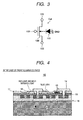
- Fig. 3 is a diagram of an equivalent circuit of the pixel cell according to this embodiment.
- the pixel cell 2A (Cel) includes, as shown in Fig. 3 , a photoelectric conversion and charge accumulation element section 111 formed in the first well 110 and one transistor 130 formed by the second well 120 and an electrode on the second substrate surface 102 side.
- the pixel cell Cel As described above, the pixel cell Cel according to this embodiment is the back-illuminated type and has the double-well structure. In the pixel cell Cel, accumulated charges and channel currents are identical carriers. Further, the pixel cell Cel has a one-transistor architecture (structure) in which one transistor has functions of a readout transistor, a reset transistor, and a selection transistor.
- the pixel cell Cel is the back-illuminated type and adopts the double-well structure and does not adopt a single-well modulation system. A reason for this is explained below.
- the single-well structure Even if the single-well structure has a high modulation degree and high conversion efficiency, the single-well structure is susceptible to a defect.
- pixel fluctuation in linearity non-linearity like as cat's paw
- the pixel cell Cel is the back-illuminated type and has the double-well structure, accumulated charges and channel currents are identical carriers, and pixel separation can be performed by an independent carrier. Therefore, the transistor structure does not need to be a ring.
- the transistor can be configured by so-called unidirectional structure of drain (D)/gate (G) /source (S) same as the structure of the normal transistor.
- the structure for discharging signal carriers to the drain of the transistor 130 is adopted.
- the pixel cell structure according to this embodiment since the pixel cell structure according to this embodiment only has to be the single-layer gate structure rather than the double-layer gate structure, special work is unnecessary for the element separation area.
- a drain, a source, and a gate can be shared between adjacent pixels. Therefore, it is possible to remarkably improve layout efficiency and perform pixel size shrinking.
- a reflector structure which makes use of metal of wiring or the like, can be provided in the space.
- Si silicon
- the double-well structure since the double-well structure is adopted, there is an advantage that it is possible to discharge dark current electrons generated on the Si surface from the channel to the drain and completely shut out dark currents and white dots caused in the interface.
- An array structure for realizing pixel size shrinking, a configuration including a reflector, a configuration and functions of a signal readout processing system, and nondestructive readout processing for signals are described in detail later.
- Electron and hole pairs are generated mainly by a photoelectric effect in the n-type first well 110 in the pixel cell.
- the generated holes are discharged to the outside through the p-type element separation layer 140 forming a wall surface of the cell.
- a signal of the accumulated charges is amplified and detected through the transistor 130, the accumulated charges are discharged as appropriate, and control of color mixture and a saturate charge amount is performed.
- the thickness of a semiconductor layer of a sensor of the solid-state imaging device 1 is about 2 ⁇ m to 10 ⁇ m, which is the thickness enough for displaying quantum efficiency of photoelectric conversion in a wavelength range of light.
- the thickness of the semiconductor substrate needs to be kept at the thickness (up to several hundreds ⁇ m) that makes an element less easily cracked. Therefore, a leak current between a source and a drain through a substrate of the element may be unable to be neglected and may pose a problem.
- the thickness of the element is sufficiently small, it is possible to reduce the leak current through the substrate and prevent the problem.
- the solid-state imaging device 1 is examined more in detail below.
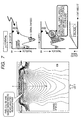
- Fig. 4 is a diagram for explaining what kind of relation the wavelength of incident light has with an arrangement of transistors in the case of a front-illuminated BMCD.
- a front-illuminated BMCD 10 shown in Fig. 4 an insulating film 11, transparent electrodes 12, light shielding electrodes 13, and the like are formed on a substrate front surface side.
- Reference numeral 14 denotes lateral drains, 15 denotes a gate insulating film, and 16 denotes a silicon substrate.
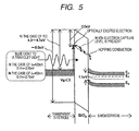
- Fig. 5 is a diagram of an overview of an energy band state formed by a transparent electrode, a gate silicon oxide film, and silicon monocrystal in the case of the front-illuminated type.
- a characteristic of a gate oxide film may be considerably different depending on a manufacturing method or processing.
- a trap that captures electrons and holes remains in the silicon oxide film.
- a trap that captures electrons is present in a position of 2.0 eV under a conduction band of the silicon oxide film.
- a band gap is about 8.0 eV.
- a work function is about 4.3 eV to 4.7 eV. Therefore, a Fermi level of the transparent electrode is located a little below the center of an energy gap of the silicon thermal oxide film.
- this energy is substantially equal to a position of an energy level of an electron trap in the oxide film measured from the Fermi level of the transparent electrode.
- the electrons captured by the trap are ejected again by an electric field, flow into the conduction band of the silicon monocrystal according to hopping conduction, bring the gate electrode and the silicon into a weak conduction state, and cause fluctuation in the transistor characteristic and a signal amount.
- the rear illumination does not have the disadvantage of the front illumination.
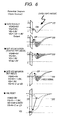
- Fig. 6 is a diagram of a change in potential with respect to electrons in a semiconductor substrate in a direction perpendicular to a semiconductor substrate surface in each of regions according to a potential state change of the device shown in Figs. 2A and 2B .
- voltage VGND of the well contact electrode 170 is set to 0 V.
- the source voltage VS thereof is about 1. 6 V to 1.4 V. Accumulated charges (electrons) decrease and a channel electron current flowing from the source to the drain is modulated and decreases according to the decrease in the accumulated charges. If this current change is measured, an amount of change of charges of the accumulated electrons is obtained.
- the source voltage VS thereof is equal to or lower than 1.2 V. Electrons are accumulated in the potential well formed near the semiconductor surface in the gate region between the source and the drain of the transistor 130.
- the source voltage VS thereof has high impedance Hi-Z or LD.
- the accumulated electrons overflow.
- the pixel cell Cel is saturated. At this point, a signal is held.
- the gate voltage VG of the transistor 130 is set to 0 V to -1.0 V and the drain voltage VD thereof is set to be equal to or higher than 3.0 V, for example, set to 3.7 V, the source voltage VS thereof has high impedance Hi-Z or LD.
- the electrons present in the accumulation well are discharged to the outside through the drain electrode.
- the drain voltage VD is modulated and, in some case, both the drain voltage VD and the gate voltage VG are modulated (in the example shown in Fig. 6 , a potential difference between the drain and the gate is increased) to discharge signal charges (electrons) accumulated in the drain electrode.
- a so-called gamma ( ⁇ ) characteristic is given to the pixel cell to increase a degree of modulation and conversion efficiency when illuminance is low.
- the ⁇ characteristic is applied to a high dynamic range (DR).
- the ⁇ characteristic of the pixel cell is explained below.
- Fig. 7 is a diagram of an example of a potential distribution in an a-a' line shown in Fig. 2A .
- a sensor accumulation region has a broad potential shape. Therefore, a capacity of the double well changes according to a signal amount and has nonlinearity (the ⁇ characteristic).
- the ⁇ characteristic is positively utilized and, as shown in Fig. 2B , a rather deep n-type gamma pocket 180 for accumulating small signals is provided.
- the pixel cell Cel has the structure in which a capacity thereof increases during a large signal output and realizes the high dynamic range (DR) according to the ⁇ characteristic.
- Fig. 8 is a schematic diagram of a configuration of the signal readout processing system according to this embodiment.
- the column (X) direction control circuit 4 includes a CDS circuit 41.
- An accumulated signal of the pixel cell Cel in an ON state is transferred to the CDS circuit 41 through a signal transmission line SL and a switch SW.
- Reference sign IS denotes a current source for forming a source follower.
- Fig. 9 is a diagram of an example of a layout of pixel cells in the pixel section according to this embodiment.
- Fig. 10A is a simplified sectional view taken along an a-a' line shown in Fig. 9 .
- Fig. 10B is a simplified sectional view taken along a b-b' line shown in Fig. 9 .
- the pixel cells Cel are arranged in a matrix shape.
- a Bayer array is adopted.
- a p-type element separation layer (conductive layer) 140A is formed on sidewalls of the first well 110 and the second well 120.
- a source region 141 and a drain region 142 including the n + layer forming the transistor 130 are formed in the p-type element separation layer 140A.
- a well contact region 143 is formed on the source region 141 side or the drain region 142 side. In this example, the well contact region 143 is formed on the source region 141 side.
- a gate contact electrode 190 is formed in a position opposed to the p-type element separation layer 140A.
- a reflector 200 is formed on a front side (a side where light is not irradiated) of the gate electrode 131 of the pixel cell Cel excluding the element separation layer 140A.
- the pixel cells are arranged to share, with adjacent pixel cells, a part or a plurality of contacts of the drain, the source, the wells, or the gate. This makes it possible to improve the layout efficiency.
- the pixel cell Cel can be configured by one transistor, the contacts of the drain, the source, the gate, and the well are arranged in the four directions on the pixel separation layers and the gate occupies the entire pixel. Therefore, random noise of the transistor is remarkably reduced.
- a drain contact DCNT and a source contact SCNT are shared by pixel cells adjacent to each other in a Y direction (a vertical direction or a row direction) of X and Y directions shown in the figure.
- a gate contact GCNT and a well contact WCNT are shared by pixel cells adjacent to each other in the X direction (a horizontal direction or a column direction).
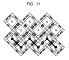
- the drain contact DCNT, the source contact SCNT, the gate contact GCMT, and the well (substrate) contact WCNT can be arranged in the four direction of the gate. Therefore, as shown in Fig. 11 , the layout can be used in a so-called zigzag array as well.
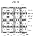
- Fig. 12 is a diagram of an example of a layout in which a gate is shared in an X direction (horizontal direction) stripe.
- the gate is shared in the horizontal stripe and the well (substrate) contact WCNT is set on the source side or the drain side. This makes it possible to easily form the reflector 200.
- the well (substrate) contact WCNT may be arranged in every other column in the X (horizontal) direction.
- Fig. 13 is a diagram of an example of a layout in which the drain side is pinched.
- drain width is reduced, i.e., pinched to secure withstanding pressure.
- Fig. 14 is a diagram of another example of the layout of the pixel cells in the pixel section according to this embodiment.
- Fig. 15A is a simplified sectional view taken along an a-a' line shown in Fig. 14 .
- Fig. 15B is a simplified sectional view taken along a b-b' line shown in Fig. 14 .
- the layout shown in Fig. 14 is the same as that of the example shown in Fig. 9 .
- the well (substrate) contact WCNT is formed on the first substrate surface 101 (rear surface) side rather than the second substrate surface 102 side.
- the gate electrode 131 is formed over the entire pixel cell including the p-type element separation layer 140A on the second substrate surface 102 side.
- a not-shown light shielding film for color mixture prevention can also be used as not-shown wiring.
- wiring of the reflector 200 is symmetrically formed. This is advantageous in terms of withstanding pressure.
- the reflector 200 is explained more in detail.
- a space is formed on the gate electrode 131 of the transistor 130. Therefore, a reflector structure, which makes use of metal of wiring or the like, can be provided in the space.
- the substrate is relatively thick (about 6 ⁇ m to 10 ⁇ m) and can be applied to, for example, a night vision monitor camera by making use of reflection of near infrared light by the reflector 200.
- a silicon substrate needs to have the thickness of 2 ⁇ m to 3 ⁇ m is necessary for visible light and has to receive light with an angle of incidence up to about 25 degrees.
- About 1:2 in an aspect ratio is a limit. Therefore, it is said that about 1 ⁇ m to 1.5 ⁇ m is a limit of the pixel size.
- the silicon substrate has to have only a half thickness 1 ⁇ m to 1.5 ⁇ m. Therefore, as the pixel size, a sub-micron pixel is possible.
- the reflector 200 is wiring of metal (A1, etc.). This configuration example is described later.
- a reflector may be formed of a nonconductive insulating film or the like.
- drain contacts are divided into two or more groups in a column to share a column circuit in the column direction (X direction) control circuit 4 and realize downsizing.
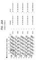
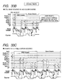
- Figs. 17A and 17B are diagrams of an example of a pixel cell array of a contact sharing pixel section.
- Fig. 17A is a diagram of an example of a layout of pixel cells.
- Fig. 17B is a diagram of a pattern layout corresponding to Fig. 17A .
- Fig. 18 is a diagram of an equivalent circuit in which the layout shown in Fig. 17A is adopted and signal processing system and pixel sections that share a column circuit are simplified.
- two vertical lines share a drain.
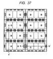
- Fig. 17A selected and shown sixteen cells Cel are arranged in a matrix shape.
- the Bayer array is adopted.
- a pixel cell Cel11 of G (green, Gr) is arranged in the first row, first column, a pixel cell Cel12 of B (blue) is arranged in the first row, second column, a pixel cell Cel21 of R (red) is arranged in the second row, first column, and a pixel cell Cel22 of G (Gb) is arranged in the second row, second column.
- a pixel cell Cel13 of G (Gr) is arranged in the first row, third column
- a pixel cell Cel14 of B is arranged in the first row, fourth column
- a pixel cell Cel23 of R is arranged in the second row, third column
- a pixel cell Cel24 of G (Gb) is arranged in the second row, second column.
- a pixel cell Cel31 of G is arranged in the third row, first column, a pixel cell Cel32 of B is arranged in the third row, second column, a pixel cell Cel41 of R is arranged in the fourth row, first column, and a pixel cell Cel42 of G (Gb) is arranged in the fourth row, second column.
- a pixel cell Cel33 of G (Gr) is arranged in the third row, third column
- a pixel cell Cel34 of B is arranged in the third row, fourth column
- a pixel cell Cel43 of R is arranged in the fourth row, third column
- a pixel cell Cel44 of G (Gb) is arranged in the fourth row, fourth column.
- pixel cells in an odd number row and an even number row adjacent to each other share a drain contact.
- the pixel cells Cel11 and Cel21 share the drain contact DCNT and the pixel cells Cel31 and Cel41 share the drain contact DCNT.
- the pixel cells Cel12 and Cel22 share the drain contact DCNT and the pixel cells Cel32 and Cel42 share the drain contact DCNT.
- the pixel cells Cel13 and Cel23 share the drain contact DCNT and the pixel cells Cel33 and Cel43 share the drain contact DCNT.
- the pixel cells Cel14 and Cel24 share the drain contact DCNT and the pixel cells Cel34 and Cel44 share the drain contact DCNT.
- a group GRP1 is formed by the pixel cells Cel11 to Cel14 in the first row and the pixel cells Cel21 to Cel24 in the second row that share the drain contact DCNT.
- a group GRP2 is formed by the pixel cells Cel31 to Cel34 in the third row and the pixel cells Cel41 to Cel44 in the fourth row that share the drain contact DCNT.
- pixel cells adjacent to each other share the source contact SCNT.
- the pixel cell Cel21 of the group GRP1 and the pixel cell CEL31 of the group GRP2 share the source contact SCNT.
- the pixel cell Cel22 of the group GRP1 and the pixel cell Cel32 of the group GRP2 share the source contact SCNT.
- the pixel cell Cel23 of the group GRP1 and the pixel cell Cel33 of the group GRP2 share the source contact SCNT.
- the pixel cell Cel24 of the group GRP1 and the pixel cell Cel34 of the group GRP2 share the source contact SCNT.
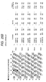
- reference signs LGND1 to LGND5 and the like denote ground lines connected to the well contact WCNT
- LSGN1 to LSGN4 and the like denote signal lines connected to the source contact SCNT
- LGT1 to LGT3 and the like denote gate lines connected to the gate contact
- LDRN1 to LDRN 4 and the like denote drain lines connected to the drain contact.
- the ground line LGND and the signal line LSGN are wired for each of the columns in the Y direction (the row direction).
- the gate line LGT and the drain line LDRN are wired for each of the rows in the X direction (the column direction).
- the ground line LGND, the signal line LSGN, the gate line LGT, and the drain line LDRN are formed by a laminated structure of the wiring.
- the ground line LGND is formed by first metal wiring (1MT) in a bottom layer.
- the signal line LSGN is formed by second metal wiring (2MT) in a layer second from the bottom.
- the gate line LGT and the drain line LDRN are formed by third metal wiring (3MT) of a top layer via an insulating film provided between the lines while maintaining insulating properties.
- 3MT third metal wiring
- the drain line LDRN formed by the third metal wiring is backed by, for example, A1 wiring Lal to reduce resistance as measures against IR drop.
- the gate contact GCNT and the well (substrate) contact WCNT are formed to face opposite directions in the X direction (the column direction).
- the gate contact GCNT and the well (substrate) contact WCNT are formed to face opposite directions as well.
- the gate contact GCNT of the pixel cell Cel11 in the first column is formed on the left side in the figure in the X direction and the well contact WCNT is formed on the right side in the figure in the X direction.
- the gate contact GCNT is formed on the right side in the figure in the X direction and the well contact WCNT is formed on the left side in the figure in the X direction.
- the gate of the transistor 130 of the pixel cell Cel11 is connected to the gate line LGT1 via the gate contact GCNT.
- the well contact WCNT is connected to the ground line LGND2 wired in the second column.
- the gate of the transistor 130 of the pixel cell Cel21 is connected to the gate line LGT1 via the gate contact GCNT.
- the well contact WCNT is connected to the ground line LGND1 wired in the first column.
- the gate contact GCNT is formed on the right side in the figure in the X direction.
- the well contact WCNT is formed on the left side in the figure in the X direction.
- the gate contact GCNT of the pixel cell Cel22 in the second column is formed on the left side in the figure in the X direction.
- the well contact WCNT is formed on the right side in the figure in the X direction.
- the gate of the transistor 130 of the pixel cell Cel12 is connected to the gate line LGT1 via the gate contact GCNT.
- the well contact WCNT is connected to the ground line LGND2 wired in the second column.
- the gate of the transistor 130 of the pixel cell Cel22 is connected to the gate line LGT1 via the gate contact GCNT.
- the well contact WCNT is connected to the ground line LGND3 wired in the third column.
- the gate contact GCNT of the pixel cell Cel13 in the third column is formed on the left side in the figure in the X direction and the well contact WCNT is formed on the right side in the figure in the X direction.
- the gate contact GCNT of the pixel cell Cel23 in the first column is formed on the right side in the figure in the X direction and the well contact WCNT is formed on the left side in the figure in the X direction.
- the gate of the transistor 130 of the pixel cell Cel13 is connected to the gate line LGT1 via the gate contact GCNT.
- the well contact WCNT is connected to the ground line LGND4 wired in the fourth column.
- the gate of the transistor 130 of the pixel cell Cel23 is connected to the gate line LGT1 via the gate contact GCNT.
- the well contact WCNT is connected to the ground line LGND3 wired in the third column.
- the gate contact GCNT of the pixel cell Cel14 in the fourth column is formed on the right side in the figure in the X direction and the well contact WCNT is formed on the left side in the figure in the X direction.
- the gate contact GCNT of the pixel cell Cel24 in the second column is formed on the left side in the figure in the X direction and the well contact WCNT is formed on the right side in the figure in the X direction.
- the gate of the transistor 130 of the pixel cell Cel14 is connected to the gate line LGT1 via the gate contact GCNT.
- the well contact WCNT is connected to the ground line LGND4 wired in the fourth column.
- the gate of the transistor 130 of the pixel cell Cel24 is connected to the gate line LGT1 via the gate contact GCNT.
- the well contact WCNT is connected to the ground line LGND5 (not shown) wired in the fifth column.
- the groups GRP2 and GRP3 are basically formed in the same pattern. Therefore, detailed explanation of the groups GRP2 and GRP3 is omitted.
- the signal lines LSGN1 to LSGN4 and the like are respectively divided into two signal lines LSGN1-T and LSGN1-B, LSGN2-T and LSGN2-B, LSGN3-T and LSGN3-B, and LSGN4-T and LSGN4-B and the like.
- An odd number group select switch (a top switch) OGSW1 and an even number group select switch (a bottom switch) EGSW1 are provided and a top switch OGSW2 and a bottom switch EGSW2 are provided in a unit of two columns.
- the signal lines LSGN1-T and LSGN2-T are connected to two switching terminals of the top switch OGSW1.
- the signal lines LSGN1-B and LSGN2-B are connected to two switching terminals of the bottom switch EGSW1.
- the signal lines LSGN1-T and LSGN2-T are connected to the source contact SCNT of the odd number groups GRP1, GRP3 and the like.
- the signal lines LSGN1-B and LSGN2-B are connected to the source contact SCNT of the even number groups GRP2, GRP4 and the like.
- the signal lines LSGN3-T and LSGN4-T are connected to two switching terminals of the top switch OGSW2.
- the signal lines LSGN3-B and LSGN3-B are connected to two switching terminals of the bottom switch EGSW2.
- the signal lines LSGN3-T and LSGN4-T are connected to the source contact SCNT of the odd number groups GRP1, GRP3 and the like.
- the signal lines LSGN3-B and LSGN4-B are connected to the source contact SCNT of the even number groups GRP2, GRP4 and the like.
- Fixed terminals of the top switches OGSW1, OGSW2 and the like are connected to a first signal transfer line LSTM1.
- Fixed terminals of the bottom switches EGSW1 and EGSW2 are connected to a second signal transfer line LSTM2.
- a current source I401 is connected to the first signal transfer line LSTM1.
- a connection point of the current source I401 and the first signal transfer line LSTM1 is connected to a comparator 401 of a column circuit 400 via a capacitor C401.
- An inverting input (-) of the comparator 401 is connected to the capacitor C401. Reference potential is given to a non-inverting input (+) thereof.
- a reset switch 402 is connected between the inverting input (-) and an output of the comparator 401.
- the switch 402 is formed by, for example, a MOS transistor.
- a current source I411 is connected to the second signal transfer line LSTM2.
- a connection point of the current source I411 and the second signal transfer line LSTM2 is connected to a comparator 411 of a column circuit 410 via a capacitor 411.
- An inverting input (-) of the comparator 411 is connected to the capacitor C411. Reference potential is given to a non-inverting input (+) thereof.
- a reset switch 412 is connected between the inverting input (-) and an output of the comparator 411.
- the switch 412 is formed by, for example, a MOS transistor.
- Figs. 19A and 19B are diagrams of signal output orders in the square array shown in Figs. 17A and 17B .
- Fig. 19A is a diagram of a signal output order for outputting signals when horizontal columns are not shared.
- Fig. 19B is a diagram of a signal output order for outputting signals when horizontal columns are shared.
- Figs. 19A and 19B to arrange pixel cells in the signal output orders, an arrangement of the pixel cells is vertically reversed from that shown in the layout diagram.
- rows and columns are represented as V rows and H columns and numbers are affixed to the respective rows and columns. Numbers corresponding to RGB of pixel cells and a matrix array are given to output signals.
- a signal in the first row, first column is represented as R11 and a signal in the first row, second column is represented as G12.
- signals are outputted in order according to a pixel cell array both on a bottom side and a top side.
- signals are outputted in a time division manner.
- first, signals of pixel cells G12, G14, and the like are read out on the bottom side and signals of pixel cells B22 and B24 are readout on the top side and, second, signals of pixel cells R11, R13, and the like are read out on the bottom side and signals of pixel cells G21 and G23 are read out on the top side.
- Gb and Gr are alternately read out for every two lines and read out dividedly in an odd number column and an even number column.
- the horizontal wiring of the drain line LDRN is backed by Al for a reduction in resistance, it is possible to prevent a fall in signal voltage transmitted to the drain line.
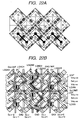
- Figs. 20A and 20B are diagrams of a zigzag array formed by rotating the square array shown in Figs. 17A and 17B by 45 degrees.
- Fig. 20A is a diagram of an example of a layout of pixel cells.
- Fig. 20B is a diagram of a pattern layout corresponding to Fig. 20A .
- Fig. 21 is a diagram of an equivalent circuit in which the layout shown in Fig. 20A is adopted and a signal processing system and a pixel section that share a column circuit are simplified.
- the zigzag array can be realized by simply rotating an electrode and the structure below the electrode by 45 degrees and contriving wiring for the zigzag array.
- a basic operation is the same as that in the case of the square array shown in Figs. 17A and 17B and Fig. 18 . It is possible to perform reset separately for an odd number and an even number and sample signals in order of a D phase Do of the odd number, a P phase Po of the odd number, a D phase De of the even number, and a P phase Pe of the even number. It is possible to perform arbitrary adding processing of signals from same color pixels with digital addition both vertically and horizontally (counter addition vertically).
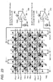
- Figs. 22A and 22B are diagrams of another zigzag array formed by rotating the square array shown in Figs. 17A and 17B .
- Fig. 22A is a diagram of an example of a layout of pixel cells.
- Fig. 22B is a diagram of a pattern layout corresponding to Fig. 22A .
- Fig. 23 is a diagram of an equivalent circuit in which the layout shown in Fig. 22A is adopted and a signal processing system and a pixel section that share a column circuit are simplified.
- a form of signal readout is the same as that in the case of Figs. 17A and 17B and Fig. 18 .
- a column at the bottom and a column at the top are alternately arranged.
- a basic operation is the same as that in the case of the square array shown in Figs. 17A and 17B and Fig. 18 . It is possible to perform reset separately for an odd number and an even number and sample signals in order of a D phase Do of the odd number, a P phase Po of the odd number, a D phase De of the even number, and a P phase Pe of the even number. It is possible to perform arbitrary adding processing of signals from same color pixels with digital addition both vertically and horizontally (counter addition vertically).
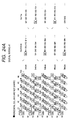
- Figs. 24A and 24B are diagrams of signal output orders in the zigzag array shown in Figs. 20A and 20B .
- Fig. 24A is a diagram of a signal output order for outputting signals when horizontal columns are not shared.
- Fig. 24B is a diagram of a signal output order for outputting signals when horizontal columns are shared.
- rows and columns are represented as V rows and H columns and numbers are affixed to the respective rows and columns. Numbers corresponding to RGB of pixel cells and a matrix array are given to output signals.
- signals are outputted in order according to a pixel cell array both on a bottom side and a top side.
- signals are outputted in a time division manner.
- first, signals of pixel cells R11, R13, and the like are read out on the bottom side and signals of pixel cells G22 and G24 are readout on the top side and, second, signals of pixel cells B12, B14, and the like are read out on the bottom side and signals of pixel cells G23 and G25 are read out on the top side.
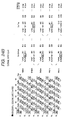
- Figs. 25A and 25B are diagrams of signal output orders in the zigzag array shown in Figs. 22A and 22B .
- Fig. 25A is a diagram of a signal output order for outputting signals when horizontal columns are not shared.
- Fig. 25B is a diagram of a signal output order for outputting signals when horizontal columns are shared.
- rows and columns are represented as V rows and H columns and numbers are affixed to the respective rows and columns. Numbers corresponding to RGB of pixel cells and a matrix array are given to output signals.
- signals are outputted in order according to a pixel cell array both on a bottom side and a top side.
- signals are outputted in a time division manner.
- first, signals of pixel cells R11, R13, R15, and the like are read out on the bottom side and signals of pixel cells G21, G23, and G25 are readout on the top side and, second, signals of pixel cells G22, G24, G26, and the like are read out on the bottom side and signals of pixel cells B12, B14, and B16 are read out on the top side.
- the drain contact DCNT, the source contact SCNT, the gate contact GCNT, and the well (substrate) contact WCNT can be arranged in the four direction of the gate. Therefore, as shown in Fig. 26A , an entire light sensing region is a gate region.
- the reflector 200 can be basically formed to be superimposed on the entire gate region.
- the reflector can be formed by using any wiring of a laminated structure.
- Fig. 27 is a diagram of a first example of the reflector and a wiring sharing layout.
- Fig. 28 is a diagram of a second example of the reflector and the wiring sharing layout.
- Fig. 29 is a diagram of a third example of the reflector and the wiring sharing layout.
- the gate line LGT is first metal wiring
- the drain line LDRN is second metal wiring
- the signal line LSGN and the ground line LGND are third metal wiring.
- the first metal wiring of the gate line LGT is used as the reflector 200.
- the reflector 200 is selectively formed in association with the gate region.
- the ground line LGND is first metal wiring
- the signal line LSGN is second metal wiring
- the gate line LGT and the drain line LDRN are third metal wiring.
- the first metal wiring of the ground line LGND is used as the reflector 200.
- the gate line LGT is first metal wiring
- the drain line LDRN is second metal wiring
- the signal line LSGN and the ground line LGND are third metal wiring.
- the first metal wiring of the gate line LGT is used as the reflector 200.
- the reflector 200 is formed in a stripe shape.
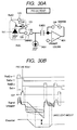
- the solid-state imaging device 1 has a pre-line reset function for improving large light amount resistance using a reset level of a preceding line as a reference level of the comparator 401 (411) of the column circuit 400 (410).
- Figs. 30A and 30B are diagrams for explaining a basic concept of pre-line reset.
- Fig. 30A is a diagram of an equivalent circuit.
- Fig. 30B is a timing chart.
- This embodiment adopts a function of reducing a residual image by performing a reset operation after injecting charges from the drain to the pixels immediately before pixel reset to saturate the pixel cells (hard resetting the pixel cells).
- Figs. 31A and 31B are schematic diagrams of a signal processing system corresponding to a hard reset function according to this embodiment.
- Fig. 31A is a diagram of an equivalent circuit.
- Fig. 31B is a timing chart.
- a transistor Q401 a drain of which is connected to power supply potential and a source of which is connected to the capacitor C401 (C411), a capacitor C402 connected between a connection point of the transistor Q401 and a ground line via a switch SW402, a current source I402 connected to the source of the transistor Q401 via a switch W403, and a current source I403 connected to a gate of the transistor Q401 are provided between the switch SW 401 and the capacitor C401 (C411) arranged between the signal transfer line and the column line 400 (410).
- the gate of the transistor Q401 is connected to a switch SW401.
- the gate voltage VG of the transistor 130 is set to 0 V to -1.0 V and the drain voltage VD thereof is set to 1.8 V
- the source voltage VS thereof is high impedance Hi-Z or LD.
- the gate voltage VG of the transistor 130 is set to 0 V to -1.0 V and the drain voltage VD thereof is set to be equal to or higher than 3.0 V, for example, set to 3.7 V
- the source voltage VS thereof is high impedance Hi-Z or LD.
- the electrons present in the accumulation well are discharged to the outside through the drain electrode.
- a circuit configuration corresponding to the analog SHD and the digital CDS can be applied to pixel cells of a so-called floating diffusion (FD) configuration as well.
- FD floating diffusion
- a ⁇ characteristic is positively given to the pixel cells.
- an inverse ⁇ correction circuit is configured by using a transistor having a back gate terminal of the same structure as the transistor 130 of the pixel cells.
- Fig. 32 is an equivalent circuit diagram for explaining a basic concept of a signal processing system including the inverse ⁇ correction circuit.
- the inverse ⁇ correction circuit 420 includes a transistor 421 having a back gate terminal, transistors 422 and 423 configuring a current mirror, a switch SW421, a capacitor C421, and current sources I421, I422, and I423.
- a source of the transistor 421 and the current source I421 are connected.
- a connection point of the source of the transistor 421 and the current source I421 is connected to the switch SW401.
- a drain of the transistor 421 is connected to a source of the transistor 422.
- a gate and a drain of the transistor 422 are connected.
- a connection point of the gate and the drain is connected to the current source I422, a gate of the transistor 423, and the switch SW421.
- a drain of the transistor 423 is connected to power supply potential.
- a source of the transistor 423 is connected to a current source I423. Connection points of the source of the transistor 423 and the current source I423 are connected to the substrate of the transistor 421 and the capacitor 401.
- the capacitor C421 is connected to the switch SW421.
- the ⁇ characteristic is reduced by the inverse ⁇ correction circuit 420, i.e., non-linearity of the ⁇ characteristic is changed to linearity to perform analog to digital conversion.
- the signal processing system according to this embodiment has the characteristics described above.
- CDS or ADC In general column digital CDS or ADC, CDS or ADC is slowly performed in one H (horizontal) period. A signal memorized in an FD is assumed.
- the pre-line reset system that makes use of a reset level of a preceding line can cope with reset of the column digital CDS.
- Figs. 33A to 33C are diagrams of a level diagram of the pre-line reset system, two-column sharing, and 2x2 pixel timing.
- Fig. 33A is a diagram of an example of working voltage.
- Fig. 33B is a diagram of an example of a still image sequence in two column sharing.
- Fig. 33C is a diagram of an example of a 2x2 pixel addition sequence.
- pixel cells are arranged in an array shape to obtain one output signal with plural pixels. This makes it possible to attain a high-Qs and low-noise dynamic range.
- a method of obtaining one output signal may be performed in a solid-state imaging element or in a signal processing IC outside the element.
- the method is performed in the signal processing IC outside the element, there is an advantage that, for example, a defective pixel can be corrected.
- a complementary color magenta is obtained. Therefore, complementary color signal processing used in a cam coder and the like can be used. As a result, color reproducibility is the same as that of the primary colors and improvement of mass productivity through sharing of color filter materials can be attained.
- the solid-state imaging device 1 it is possible to perform nondestructive readout without worsening of dark currents by continuing photoelectric conversion without resetting pixels in signal readout from pixels.
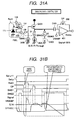
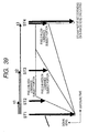
- Fig. 39 is a diagram of an example of a wide dynamic range (Wide D-Range) sequence according to the nondestructive readout.
- the vertical direction indicates a signal level and the horizontal direction indicates exposure time.
- the signal level is reset and black scan is performed.
- a threshold Vh variation image is captured.
- first intermediate scan (SCAN #1) is performed. A high-luminance image is captured and a Vth difference is obtained.
- second intermediate scan (SCAN #2) is performed. A medium-luminance image is captured and a Vth difference is obtained.
- step ST5 a wide dynamic range is realized by image combination of the high-luminance image, the medium-luminance image, and the low-luminance image. (The respective images are multiplied by time ratios and combined by level to obtain a high-DR image.)
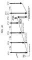
- Fig. 40 is a diagram of an example of a low-speed live view sequence according to the nondestructive readout.
- the vertical direction indicates a signal level and the horizontal direction indicates exposure time.
- the signal level is reset and black scan is performed.
- a threshold Vh variation image is captured.
- Second intermediate scan (SCAN #1) is performed. #1 image is captured and a #0Vth difference is obtained and, for example, displayed for monitoring.
- Second intermediate scan (SCAN #2) is performed. #2 image is captured and #1 Vth difference is obtained and, for example, displayed for monitoring.
- Capturing scan is performed to reset the signal level.
- Final image capturing CDS and recording in a memory are performed.
- step ST15 (a still image) is displayed in terms of 1/30s.
- the substrate 100 includes the first substrate surface 101 side on which light is irradiated and the second substrate surface 102 side on which elements are formed.
- the plural pixel cells Cel (2A) separated by the adjacent cell group and the element separation layer are formed.
- Each of the pixel cells Cel includes the first conductive (in this embodiment, n-type) well (the first well) 110 formed on the first substrate surface 101 side and the second conductive (p-type) well (the second well) 120 formed further on the second substrate surface 102 side than the first well 110.
- the n-type first well 110 functions as a light sensing section that receives light from the first substrate surface 101 side and has the photoelectric conversion function and the charge accumulation function for the received light.
- the MOS transistor 130 that detects accumulated charges in the light sensing section of the first well 110 and has the threshold modulation function is formed in the second well 120.
- a pixel can be formed by one transistor of the drain (D)/gate (G)/source (S) structure.
- D drain
- G gate
- S source
- Layout efficiency is high and a micro-pixel can be realized because the contacts of the drain, the source, the gate, and the well can be shared.
- the entire light sensing section is the gate.
- the reflector When the reflector is mounted, near infrared high sensitivity and an ultra-fine pixel can be realized.
- Noise can be reduced by the inverse ⁇ correction function.
- the solid-state imaging device having the characteristics described above can be applied as imaging devices of a digital camera and a video camera.
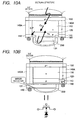
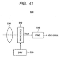
- Fig. 41 is a diagram of an example of a configuration of a camera system to which the solid-state imaging device according to this embodiment is applied.
- This camera system 500 includes, as shown in Fig. 41 , an imaging device 510 to which the solid-state imaging device 1 according to this embodiment can be applied, an optical system that guides incident light to a pixel region of the imaging device 510 (focuses a subject image), for example, a lens 520 that focuses incident light (image light) on an imaging surface, a driving circuit (DRV) 530 that drives the imaging device 510, and a signal processing circuit (PRC) 540 that processes an output signal of the imaging device 510.
- an imaging device 510 to which the solid-state imaging device 1 according to this embodiment can be applied
- an optical system that guides incident light to a pixel region of the imaging device 510 (focuses a subject image)
- a lens 520 that focuses incident light (image light) on an imaging surface
- DDRV driving circuit
- PRC signal processing circuit
- the driving circuit 503 includes a timing generator (not shown) that generates various timing signals including a start pulse and a clock pulse for driving circuits in the imaging device 510.
- the driving circuit 530 drives the imaging device 510 with a predetermined timing signal.
- the signal processing circuit 540 applies signal processing such as CDS (Correlated Double Sampling) to an output signal of the imaging device 510.
- CDS Correlated Double Sampling
- An image signal processed by the signal processing circuit 540 is recorded in a recording medium such as a memory.
- the image signal recorded in the recording medium is hard-copied by a printer or the like.
- the image signal processed by the signal processing circuit 540 is displayed as a moving image on a monitor including a liquid crystal display.
- imaging apparatuses and electronic apparatuses such as a digital camera, a monitoring camera, a camera mounted on a cellular phone, a single lens reflex camera, and a scanner
- solid-state imaging device 1 As described above, in imaging apparatuses and electronic apparatuses such as a digital camera, a monitoring camera, a camera mounted on a cellular phone, a single lens reflex camera, and a scanner, it is possible to realize a highly accurate camera by mounting the solid-state imaging device 1 as the imaging device 510.
Landscapes
- Solid State Image Pick-Up Elements (AREA)
- Transforming Light Signals Into Electric Signals (AREA)
Applications Claiming Priority (1)
| Application Number | Priority Date | Filing Date | Title |
|---|---|---|---|
| JP2007326175A JP5167799B2 (ja) | 2007-12-18 | 2007-12-18 | 固体撮像装置およびカメラ |
Publications (3)
| Publication Number | Publication Date |
|---|---|
| EP2073270A2 EP2073270A2 (en) | 2009-06-24 |
| EP2073270A3 EP2073270A3 (en) | 2012-05-16 |
| EP2073270B1 true EP2073270B1 (en) | 2014-03-19 |
Family
ID=40429769
Family Applications (1)
| Application Number | Title | Priority Date | Filing Date |
|---|---|---|---|
| EP08021947.0A Not-in-force EP2073270B1 (en) | 2007-12-18 | 2008-12-17 | Solid-state imaging device and camera |
Country Status (6)
| Country | Link |
|---|---|
| US (2) | US8106983B2 (enExample) |
| EP (1) | EP2073270B1 (enExample) |
| JP (1) | JP5167799B2 (enExample) |
| KR (1) | KR101534117B1 (enExample) |
| CN (2) | CN101465364B (enExample) |
| TW (1) | TWI416949B (enExample) |
Cited By (1)
| Publication number | Priority date | Publication date | Assignee | Title |
|---|---|---|---|---|
| US9496308B2 (en) | 2011-06-09 | 2016-11-15 | Sionyx, Llc | Process module for increasing the response of backside illuminated photosensitive imagers and associated methods |
Families Citing this family (54)
| Publication number | Priority date | Publication date | Assignee | Title |
|---|---|---|---|---|
| US7442629B2 (en) | 2004-09-24 | 2008-10-28 | President & Fellows Of Harvard College | Femtosecond laser-induced formation of submicrometer spikes on a semiconductor substrate |
| US7057256B2 (en) | 2001-05-25 | 2006-06-06 | President & Fellows Of Harvard College | Silicon-based visible and near-infrared optoelectric devices |
| JP5167799B2 (ja) * | 2007-12-18 | 2013-03-21 | ソニー株式会社 | 固体撮像装置およびカメラ |
| JP5458690B2 (ja) * | 2009-06-22 | 2014-04-02 | ソニー株式会社 | 固体撮像装置およびカメラ |
| US20100327390A1 (en) * | 2009-06-26 | 2010-12-30 | Mccarten John P | Back-illuminated image sensor with electrically biased conductive material and backside well |
| KR101893331B1 (ko) * | 2009-09-17 | 2018-08-30 | 사이오닉스, 엘엘씨 | 감광성 이미징 장치 및 이와 관련된 방법 |
| US9673243B2 (en) | 2009-09-17 | 2017-06-06 | Sionyx, Llc | Photosensitive imaging devices and associated methods |
| US9911781B2 (en) | 2009-09-17 | 2018-03-06 | Sionyx, Llc | Photosensitive imaging devices and associated methods |
| JP5564874B2 (ja) * | 2009-09-25 | 2014-08-06 | ソニー株式会社 | 固体撮像装置、及び電子機器 |
| JP5538811B2 (ja) * | 2009-10-21 | 2014-07-02 | キヤノン株式会社 | 固体撮像素子 |
| CN102104113B (zh) * | 2009-12-18 | 2014-05-07 | 中国科学院微电子研究所 | 有机场效应晶体管阈值电压的调制方法 |
| JP5458869B2 (ja) * | 2009-12-21 | 2014-04-02 | ソニー株式会社 | 固体撮像装置およびその駆動方法、カメラ |
| JP5538876B2 (ja) * | 2009-12-25 | 2014-07-02 | キヤノン株式会社 | 固体撮像装置 |
| WO2011099343A1 (en) * | 2010-02-12 | 2011-08-18 | Semiconductor Energy Laboratory Co., Ltd. | Semiconductor device and driving method thereof |
| JP5118715B2 (ja) * | 2010-03-11 | 2013-01-16 | 株式会社東芝 | 固体撮像装置 |
| US8692198B2 (en) | 2010-04-21 | 2014-04-08 | Sionyx, Inc. | Photosensitive imaging devices and associated methods |
| KR101652786B1 (ko) * | 2010-04-22 | 2016-09-12 | 삼성전자주식회사 | 단순화된 광센싱 회로 및 상기 광센싱 회로를 채용한 리모트 광터치 패널 및 영상 획득 장치 |
| US9891102B2 (en) * | 2010-04-22 | 2018-02-13 | Samsung Electronics Co., Ltd. | Simplified light sensing circuit, light sensing apparatus including the light sensing circuit, method of driving the light sensing apparatus, and image acquisition apparatus and optical touch screen apparatus including the light sensing apparatus |
| KR102056905B1 (ko) * | 2011-07-25 | 2019-12-18 | 삼성전자주식회사 | 광센싱 장치 및 그 구동 방법, 광센싱 장치를 포함하는 광터치 스크린 장치 |
| US20120146172A1 (en) | 2010-06-18 | 2012-06-14 | Sionyx, Inc. | High Speed Photosensitive Devices and Associated Methods |
| JP2012019169A (ja) * | 2010-07-09 | 2012-01-26 | Panasonic Corp | 固体撮像装置 |
| JP2012023207A (ja) * | 2010-07-14 | 2012-02-02 | Toshiba Corp | 裏面照射型固体撮像装置 |
| JP2012094672A (ja) * | 2010-10-27 | 2012-05-17 | Sony Corp | 半導体装置、および、半導体装置の製造方法 |
| US8785986B1 (en) * | 2011-02-02 | 2014-07-22 | Aptina Imaging Corporation | BCMD image sensor with junction gate for back side or front side illumination |
| JPWO2012161225A1 (ja) * | 2011-05-24 | 2014-07-31 | ソニー株式会社 | 固体撮像素子およびカメラシステム |
| US20130016203A1 (en) | 2011-07-13 | 2013-01-17 | Saylor Stephen D | Biometric imaging devices and associated methods |
| JP5791571B2 (ja) | 2011-08-02 | 2015-10-07 | キヤノン株式会社 | 撮像素子及び撮像装置 |
| JP2013084785A (ja) * | 2011-10-11 | 2013-05-09 | Sony Corp | 固体撮像装置、撮像装置 |
| JP2013090233A (ja) * | 2011-10-20 | 2013-05-13 | Sony Corp | 撮像素子およびカメラシステム |
| US9064764B2 (en) | 2012-03-22 | 2015-06-23 | Sionyx, Inc. | Pixel isolation elements, devices, and associated methods |
| US8686477B2 (en) * | 2012-07-25 | 2014-04-01 | Omnivision Technologies, Inc. | Ground contact structure for a low dark current CMOS pixel cell |
| DE102013110695A1 (de) * | 2012-10-02 | 2014-04-03 | Samsung Electronics Co., Ltd. | Bildsensor, Verfahren zum Betreiben desselben und Bildverarbeitungssystem mit demselben |
| KR20140047494A (ko) * | 2012-10-12 | 2014-04-22 | 삼성전자주식회사 | 서브픽셀, 이를 포함하는 이미지 센서, 및 이미지 센싱 시스템 |
| FR2997596B1 (fr) * | 2012-10-26 | 2015-12-04 | New Imaging Technologies Sas | Structure d'un pixel actif de type cmos |
| EP2936799B1 (en) * | 2012-12-21 | 2018-10-17 | Flir Systems, Inc. | Time spaced infrared image enhancement |
| JP6466346B2 (ja) | 2013-02-15 | 2019-02-06 | サイオニクス、エルエルシー | アンチブルーミング特性を有するハイダイナミックレンジcmos画像センサおよび関連づけられた方法 |
| JP2014199898A (ja) * | 2013-03-11 | 2014-10-23 | ソニー株式会社 | 固体撮像素子および製造方法、並びに、電子機器 |
| JP6160139B2 (ja) * | 2013-03-13 | 2017-07-12 | セイコーエプソン株式会社 | 撮像装置及び方法 |
| WO2014151093A1 (en) | 2013-03-15 | 2014-09-25 | Sionyx, Inc. | Three dimensional imaging utilizing stacked imager devices and associated methods |
| US9209345B2 (en) | 2013-06-29 | 2015-12-08 | Sionyx, Inc. | Shallow trench textured regions and associated methods |
| EP3066689B1 (en) | 2013-11-04 | 2020-07-08 | Artto Aurola | Improved semiconductor radiation detector |
| US9147704B2 (en) * | 2013-11-11 | 2015-09-29 | Omnivision Technologies, Inc. | Dual pixel-sized color image sensors and methods for manufacturing the same |
| JP6233188B2 (ja) * | 2013-12-12 | 2017-11-22 | ソニー株式会社 | 固体撮像素子およびその製造方法、並びに電子機器 |
| US9312299B2 (en) | 2014-04-10 | 2016-04-12 | Omnivision Technologies, Inc. | Image sensor with dielectric charge trapping device |
| KR102306670B1 (ko) | 2014-08-29 | 2021-09-29 | 삼성전자주식회사 | 이미지 센서 및 그 제조 방법 |
| JP6576025B2 (ja) * | 2014-09-29 | 2019-09-18 | キヤノン株式会社 | 光電変換装置、及び撮像システム |
| JP2016081950A (ja) | 2014-10-10 | 2016-05-16 | ソニー株式会社 | 画素回路および撮像装置 |
| US9843756B2 (en) * | 2015-05-27 | 2017-12-12 | Samsung Electronics Co., Ltd. | Imaging devices, arrays of pixels receiving photocharges in bulk of select transistor, and methods |
| JP6691101B2 (ja) * | 2017-01-19 | 2020-04-28 | ソニーセミコンダクタソリューションズ株式会社 | 受光素子 |
| US11769782B2 (en) * | 2018-05-02 | 2023-09-26 | Sony Semiconductor Solutions Corporation | Solid-state imaging element and imaging apparatus |
| CN108922940B (zh) * | 2018-07-17 | 2020-03-06 | 京东方科技集团股份有限公司 | 光学检测像素单元、电路、光学检测方法和显示装置 |
| CN109726718B (zh) * | 2019-01-03 | 2022-09-16 | 电子科技大学 | 一种基于关系正则化的视觉场景图生成系统及方法 |
| US20250160016A1 (en) * | 2022-01-06 | 2025-05-15 | Sony Semiconductor Solutions Corporation | Imaging device and electronic apparatus |
| CN115356545B (zh) * | 2022-08-10 | 2023-04-11 | 中国科学院近代物理研究所 | 一种用于带电粒子探测的新型像素单元结构及其使用方法 |
Family Cites Families (26)
| Publication number | Priority date | Publication date | Assignee | Title |
|---|---|---|---|---|
| JPS60140752A (ja) | 1983-12-28 | 1985-07-25 | Olympus Optical Co Ltd | 半導体光電変換装置 |
| JPH0666446B2 (ja) | 1984-03-29 | 1994-08-24 | オリンパス光学工業株式会社 | 固体撮像素子 |
| JPS6414959A (en) | 1987-04-10 | 1989-01-19 | Texas Instruments Inc | Device for sensing threshold of substrate charge modulation type transistor |
| JP2692218B2 (ja) | 1988-12-29 | 1997-12-17 | ソニー株式会社 | 固体撮像素子 |
| JPH02304973A (ja) | 1989-05-19 | 1990-12-18 | Hitachi Ltd | 固体撮像装置 |
| JPH06120473A (ja) | 1992-10-08 | 1994-04-28 | Olympus Optical Co Ltd | 固体撮像装置及びその駆動方法 |
| JPH0778959A (ja) * | 1993-09-09 | 1995-03-20 | Sony Corp | 固体撮像素子 |
| JPH1065138A (ja) | 1996-08-19 | 1998-03-06 | Sony Corp | 固体撮像素子 |
| JP3752773B2 (ja) | 1997-04-15 | 2006-03-08 | ソニー株式会社 | 固体撮像装置とその製造方法 |
| JP2935492B2 (ja) | 1997-10-30 | 1999-08-16 | イノビジョン株式会社 | 固体撮像素子及び固体撮像素子による光信号検出方法 |
| JP3759435B2 (ja) | 2001-07-11 | 2006-03-22 | ソニー株式会社 | X−yアドレス型固体撮像素子 |
| JP4109858B2 (ja) * | 2001-11-13 | 2008-07-02 | 株式会社東芝 | 固体撮像装置 |
| JP2004259733A (ja) * | 2003-02-24 | 2004-09-16 | Seiko Epson Corp | 固体撮像装置 |
| JP3829830B2 (ja) | 2003-09-09 | 2006-10-04 | セイコーエプソン株式会社 | 固体撮像装置及びその駆動方法 |
| JP4046067B2 (ja) * | 2003-11-04 | 2008-02-13 | ソニー株式会社 | 固体撮像素子の製造方法 |
| JP2005244434A (ja) | 2004-02-25 | 2005-09-08 | Sharp Corp | 固体撮像装置 |
| JP4187691B2 (ja) * | 2004-06-29 | 2008-11-26 | 富士通マイクロエレクトロニクス株式会社 | 閾値変調型イメージセンサ |
| JP2006108379A (ja) * | 2004-10-05 | 2006-04-20 | Sony Corp | 固体撮像素子及びその駆動方法 |
| KR100610481B1 (ko) * | 2004-12-30 | 2006-08-08 | 매그나칩 반도체 유한회사 | 수광영역을 넓힌 이미지센서 및 그 제조 방법 |
| JP4742602B2 (ja) * | 2005-02-01 | 2011-08-10 | ソニー株式会社 | 固体撮像装置及びその製造方法 |
| JP2006261638A (ja) * | 2005-02-21 | 2006-09-28 | Sony Corp | 固体撮像装置および固体撮像装置の駆動方法 |
| US8049293B2 (en) * | 2005-03-07 | 2011-11-01 | Sony Corporation | Solid-state image pickup device, electronic apparatus using such solid-state image pickup device and method of manufacturing solid-state image pickup device |
| JP2007326175A (ja) | 2006-06-07 | 2007-12-20 | Nihon Micro Coating Co Ltd | クリーニングテープ及び方法 |
| TWI479887B (zh) * | 2007-05-24 | 2015-04-01 | 新力股份有限公司 | 背向照明固態成像裝置及照相機 |
| JP5023808B2 (ja) * | 2007-05-24 | 2012-09-12 | ソニー株式会社 | 固体撮像装置およびカメラ |
| JP5167799B2 (ja) * | 2007-12-18 | 2013-03-21 | ソニー株式会社 | 固体撮像装置およびカメラ |
-
2007
- 2007-12-18 JP JP2007326175A patent/JP5167799B2/ja not_active Expired - Fee Related
-
2008
- 2008-12-09 US US12/331,116 patent/US8106983B2/en not_active Expired - Fee Related
- 2008-12-15 TW TW097148776A patent/TWI416949B/zh not_active IP Right Cessation
- 2008-12-16 KR KR1020080127805A patent/KR101534117B1/ko not_active Expired - Fee Related
- 2008-12-17 EP EP08021947.0A patent/EP2073270B1/en not_active Not-in-force
- 2008-12-18 CN CN2008101835900A patent/CN101465364B/zh not_active Expired - Fee Related
- 2008-12-18 CN CN201110090935.XA patent/CN102184930B/zh not_active Expired - Fee Related
-
2012
- 2012-01-12 US US13/348,760 patent/US8687101B2/en not_active Expired - Fee Related
Cited By (1)
| Publication number | Priority date | Publication date | Assignee | Title |
|---|---|---|---|---|
| US9496308B2 (en) | 2011-06-09 | 2016-11-15 | Sionyx, Llc | Process module for increasing the response of backside illuminated photosensitive imagers and associated methods |
Also Published As
| Publication number | Publication date |
|---|---|
| KR101534117B1 (ko) | 2015-07-06 |
| TW200943938A (en) | 2009-10-16 |
| CN102184930A (zh) | 2011-09-14 |
| CN101465364A (zh) | 2009-06-24 |
| US20120113292A1 (en) | 2012-05-10 |
| KR20090066227A (ko) | 2009-06-23 |
| JP5167799B2 (ja) | 2013-03-21 |
| US8106983B2 (en) | 2012-01-31 |
| EP2073270A2 (en) | 2009-06-24 |
| CN101465364B (zh) | 2011-06-08 |
| CN102184930B (zh) | 2014-02-26 |
| TWI416949B (zh) | 2013-11-21 |
| US8687101B2 (en) | 2014-04-01 |
| EP2073270A3 (en) | 2012-05-16 |
| JP2009152234A (ja) | 2009-07-09 |
| US20090153708A1 (en) | 2009-06-18 |
Similar Documents
| Publication | Publication Date | Title |
|---|---|---|
| EP2073270B1 (en) | Solid-state imaging device and camera | |
| JP5458690B2 (ja) | 固体撮像装置およびカメラ | |
| JP5651976B2 (ja) | 固体撮像素子およびその製造方法、並びに電子機器 | |
| EP2253017B1 (en) | Circuit and photo sensor overlap for backside illumination image sensor | |
| US9659984B2 (en) | Solid-state image sensor including a photoelectric conversion element, a charge conversion element, and a light shielding element, method for producing the same solid-state image sensor, and electronic apparatus including the same solid-state image sensor | |
| US20090201400A1 (en) | Backside illuminated image sensor with global shutter and storage capacitor | |
| US20130063641A1 (en) | Dual-sided image sensor | |
| JP2013084785A (ja) | 固体撮像装置、撮像装置 | |
| US20240214707A1 (en) | Solid-state imaging device, method for manufacturing solid-state imaging device, and electronic apparatus | |
| EP1684351A1 (en) | Solid-state image pickup device |
Legal Events
| Date | Code | Title | Description |
|---|---|---|---|
| PUAI | Public reference made under article 153(3) epc to a published international application that has entered the european phase |
Free format text: ORIGINAL CODE: 0009012 |
|
| AK | Designated contracting states |
Kind code of ref document: A2 Designated state(s): AT BE BG CH CY CZ DE DK EE ES FI FR GB GR HR HU IE IS IT LI LT LU LV MC MT NL NO PL PT RO SE SI SK TR |
|
| AX | Request for extension of the european patent |
Extension state: AL BA MK RS |
|
| PUAL | Search report despatched |
Free format text: ORIGINAL CODE: 0009013 |
|
| AK | Designated contracting states |
Kind code of ref document: A3 Designated state(s): AT BE BG CH CY CZ DE DK EE ES FI FR GB GR HR HU IE IS IT LI LT LU LV MC MT NL NO PL PT RO SE SI SK TR |
|
| AX | Request for extension of the european patent |
Extension state: AL BA MK RS |
|
| RIC1 | Information provided on ipc code assigned before grant |
Ipc: H01L 27/146 20060101AFI20120410BHEP |
|
| 17P | Request for examination filed |
Effective date: 20121115 |
|
| AKX | Designation fees paid |
Designated state(s): DE FR GB |
|
| 17Q | First examination report despatched |
Effective date: 20130319 |
|
| GRAP | Despatch of communication of intention to grant a patent |
Free format text: ORIGINAL CODE: EPIDOSNIGR1 |
|
| INTG | Intention to grant announced |
Effective date: 20131011 |
|
| GRAS | Grant fee paid |
Free format text: ORIGINAL CODE: EPIDOSNIGR3 |
|
| GRAA | (expected) grant |
Free format text: ORIGINAL CODE: 0009210 |
|
| AK | Designated contracting states |
Kind code of ref document: B1 Designated state(s): DE FR GB |
|
| REG | Reference to a national code |
Ref country code: GB Ref legal event code: FG4D |
|
| REG | Reference to a national code |
Ref country code: DE Ref legal event code: R096 Ref document number: 602008030931 Country of ref document: DE Effective date: 20140430 |
|
| REG | Reference to a national code |
Ref country code: DE Ref legal event code: R097 Ref document number: 602008030931 Country of ref document: DE |
|
| PLBE | No opposition filed within time limit |
Free format text: ORIGINAL CODE: 0009261 |
|
| STAA | Information on the status of an ep patent application or granted ep patent |
Free format text: STATUS: NO OPPOSITION FILED WITHIN TIME LIMIT |
|
| 26N | No opposition filed |
Effective date: 20141222 |
|
| REG | Reference to a national code |
Ref country code: DE Ref legal event code: R097 Ref document number: 602008030931 Country of ref document: DE Effective date: 20141222 |
|
| REG | Reference to a national code |
Ref country code: DE Ref legal event code: R084 Ref document number: 602008030931 Country of ref document: DE |
|
| REG | Reference to a national code |
Ref country code: DE Ref legal event code: R084 Ref document number: 602008030931 Country of ref document: DE Effective date: 20150410 |
|
| GBPC | Gb: european patent ceased through non-payment of renewal fee |
Effective date: 20141217 |
|
| REG | Reference to a national code |
Ref country code: FR Ref legal event code: ST Effective date: 20150831 |
|
| PG25 | Lapsed in a contracting state [announced via postgrant information from national office to epo] |
Ref country code: GB Free format text: LAPSE BECAUSE OF NON-PAYMENT OF DUE FEES Effective date: 20141217 |
|
| PG25 | Lapsed in a contracting state [announced via postgrant information from national office to epo] |
Ref country code: FR Free format text: LAPSE BECAUSE OF NON-PAYMENT OF DUE FEES Effective date: 20141231 |
|
| PGFP | Annual fee paid to national office [announced via postgrant information from national office to epo] |
Ref country code: DE Payment date: 20201211 Year of fee payment: 13 |
|
| REG | Reference to a national code |
Ref country code: DE Ref legal event code: R119 Ref document number: 602008030931 Country of ref document: DE |
|
| PG25 | Lapsed in a contracting state [announced via postgrant information from national office to epo] |
Ref country code: DE Free format text: LAPSE BECAUSE OF NON-PAYMENT OF DUE FEES Effective date: 20220701 |