EP2064734B1 - Method of printing transferable functional structures - Google Patents
Method of printing transferable functional structures Download PDFInfo
- Publication number
- EP2064734B1 EP2064734B1 EP07842903.2A EP07842903A EP2064734B1 EP 2064734 B1 EP2064734 B1 EP 2064734B1 EP 07842903 A EP07842903 A EP 07842903A EP 2064734 B1 EP2064734 B1 EP 2064734B1
- Authority
- EP
- European Patent Office
- Prior art keywords
- layers
- layer
- release
- substrate
- functional
- Prior art date
- Legal status (The legal status is an assumption and is not a legal conclusion. Google has not performed a legal analysis and makes no representation as to the accuracy of the status listed.)
- Active
Links
Images


Classifications
-
- H—ELECTRICITY
- H10—SEMICONDUCTOR DEVICES; ELECTRIC SOLID-STATE DEVICES NOT OTHERWISE PROVIDED FOR
- H10F—INORGANIC SEMICONDUCTOR DEVICES SENSITIVE TO INFRARED RADIATION, LIGHT, ELECTROMAGNETIC RADIATION OF SHORTER WAVELENGTH OR CORPUSCULAR RADIATION
- H10F10/00—Individual photovoltaic cells, e.g. solar cells
- H10F10/10—Individual photovoltaic cells, e.g. solar cells having potential barriers
- H10F10/16—Photovoltaic cells having only PN heterojunction potential barriers
- H10F10/163—Photovoltaic cells having only PN heterojunction potential barriers comprising only Group III-V materials, e.g. GaAs/AlGaAs or InP/GaInAs photovoltaic cells
-
- B—PERFORMING OPERATIONS; TRANSPORTING
- B81—MICROSTRUCTURAL TECHNOLOGY
- B81C—PROCESSES OR APPARATUS SPECIALLY ADAPTED FOR THE MANUFACTURE OR TREATMENT OF MICROSTRUCTURAL DEVICES OR SYSTEMS
- B81C1/00—Manufacture or treatment of devices or systems in or on a substrate
- B81C1/00436—Shaping materials, i.e. techniques for structuring the substrate or the layers on the substrate
- B81C1/00444—Surface micromachining, i.e. structuring layers on the substrate
- B81C1/0046—Surface micromachining, i.e. structuring layers on the substrate using stamping, e.g. imprinting
-
- B—PERFORMING OPERATIONS; TRANSPORTING
- B82—NANOTECHNOLOGY
- B82Y—SPECIFIC USES OR APPLICATIONS OF NANOSTRUCTURES; MEASUREMENT OR ANALYSIS OF NANOSTRUCTURES; MANUFACTURE OR TREATMENT OF NANOSTRUCTURES
- B82Y10/00—Nanotechnology for information processing, storage or transmission, e.g. quantum computing or single electron logic
-
- B—PERFORMING OPERATIONS; TRANSPORTING
- B82—NANOTECHNOLOGY
- B82Y—SPECIFIC USES OR APPLICATIONS OF NANOSTRUCTURES; MEASUREMENT OR ANALYSIS OF NANOSTRUCTURES; MANUFACTURE OR TREATMENT OF NANOSTRUCTURES
- B82Y20/00—Nanooptics, e.g. quantum optics or photonic crystals
-
- B—PERFORMING OPERATIONS; TRANSPORTING
- B82—NANOTECHNOLOGY
- B82Y—SPECIFIC USES OR APPLICATIONS OF NANOSTRUCTURES; MEASUREMENT OR ANALYSIS OF NANOSTRUCTURES; MANUFACTURE OR TREATMENT OF NANOSTRUCTURES
- B82Y40/00—Manufacture or treatment of nanostructures
-
- H—ELECTRICITY
- H01—ELECTRIC ELEMENTS
- H01L—SEMICONDUCTOR DEVICES NOT COVERED BY CLASS H10
- H01L21/00—Processes or apparatus adapted for the manufacture or treatment of semiconductor or solid state devices or of parts thereof
- H01L21/67—Apparatus specially adapted for handling semiconductor or electric solid state devices during manufacture or treatment thereof; Apparatus specially adapted for handling wafers during manufacture or treatment of semiconductor or electric solid state devices or components ; Apparatus not specifically provided for elsewhere
- H01L21/683—Apparatus specially adapted for handling semiconductor or electric solid state devices during manufacture or treatment thereof; Apparatus specially adapted for handling wafers during manufacture or treatment of semiconductor or electric solid state devices or components ; Apparatus not specifically provided for elsewhere for supporting or gripping
- H01L21/6835—Apparatus specially adapted for handling semiconductor or electric solid state devices during manufacture or treatment thereof; Apparatus specially adapted for handling wafers during manufacture or treatment of semiconductor or electric solid state devices or components ; Apparatus not specifically provided for elsewhere for supporting or gripping using temporarily an auxiliary support
-
- H—ELECTRICITY
- H01—ELECTRIC ELEMENTS
- H01L—SEMICONDUCTOR DEVICES NOT COVERED BY CLASS H10
- H01L21/00—Processes or apparatus adapted for the manufacture or treatment of semiconductor or solid state devices or of parts thereof
- H01L21/70—Manufacture or treatment of devices consisting of a plurality of solid state components formed in or on a common substrate or of parts thereof; Manufacture of integrated circuit devices or of parts thereof
- H01L21/77—Manufacture or treatment of devices consisting of a plurality of solid state components or integrated circuits formed in, or on, a common substrate
- H01L21/78—Manufacture or treatment of devices consisting of a plurality of solid state components or integrated circuits formed in, or on, a common substrate with subsequent division of the substrate into plural individual devices
- H01L21/7806—Manufacture or treatment of devices consisting of a plurality of solid state components or integrated circuits formed in, or on, a common substrate with subsequent division of the substrate into plural individual devices involving the separation of the active layers from a substrate
- H01L21/7813—Manufacture or treatment of devices consisting of a plurality of solid state components or integrated circuits formed in, or on, a common substrate with subsequent division of the substrate into plural individual devices involving the separation of the active layers from a substrate leaving a reusable substrate, e.g. epitaxial lift off
-
- H—ELECTRICITY
- H10—SEMICONDUCTOR DEVICES; ELECTRIC SOLID-STATE DEVICES NOT OTHERWISE PROVIDED FOR
- H10D—INORGANIC ELECTRIC SEMICONDUCTOR DEVICES
- H10D62/00—Semiconductor bodies, or regions thereof, of devices having potential barriers
- H10D62/80—Semiconductor bodies, or regions thereof, of devices having potential barriers characterised by the materials
- H10D62/81—Semiconductor bodies, or regions thereof, of devices having potential barriers characterised by the materials of structures exhibiting quantum-confinement effects, e.g. single quantum wells; of structures having periodic or quasi-periodic potential variation
- H10D62/815—Semiconductor bodies, or regions thereof, of devices having potential barriers characterised by the materials of structures exhibiting quantum-confinement effects, e.g. single quantum wells; of structures having periodic or quasi-periodic potential variation of structures having periodic or quasi-periodic potential variation, e.g. superlattices or multiple quantum wells [MQW]
- H10D62/8161—Semiconductor bodies, or regions thereof, of devices having potential barriers characterised by the materials of structures exhibiting quantum-confinement effects, e.g. single quantum wells; of structures having periodic or quasi-periodic potential variation of structures having periodic or quasi-periodic potential variation, e.g. superlattices or multiple quantum wells [MQW] potential variation due to variations in composition or crystallinity, e.g. heterojunction superlattices
- H10D62/8162—Semiconductor bodies, or regions thereof, of devices having potential barriers characterised by the materials of structures exhibiting quantum-confinement effects, e.g. single quantum wells; of structures having periodic or quasi-periodic potential variation of structures having periodic or quasi-periodic potential variation, e.g. superlattices or multiple quantum wells [MQW] potential variation due to variations in composition or crystallinity, e.g. heterojunction superlattices having quantum effects only in the vertical direction, i.e. layered structures having quantum effects solely resulting from vertical potential variation
- H10D62/8164—Semiconductor bodies, or regions thereof, of devices having potential barriers characterised by the materials of structures exhibiting quantum-confinement effects, e.g. single quantum wells; of structures having periodic or quasi-periodic potential variation of structures having periodic or quasi-periodic potential variation, e.g. superlattices or multiple quantum wells [MQW] potential variation due to variations in composition or crystallinity, e.g. heterojunction superlattices having quantum effects only in the vertical direction, i.e. layered structures having quantum effects solely resulting from vertical potential variation comprising only semiconductor materials
-
- H—ELECTRICITY
- H10—SEMICONDUCTOR DEVICES; ELECTRIC SOLID-STATE DEVICES NOT OTHERWISE PROVIDED FOR
- H10D—INORGANIC ELECTRIC SEMICONDUCTOR DEVICES
- H10D62/00—Semiconductor bodies, or regions thereof, of devices having potential barriers
- H10D62/80—Semiconductor bodies, or regions thereof, of devices having potential barriers characterised by the materials
- H10D62/82—Heterojunctions
- H10D62/824—Heterojunctions comprising only Group III-V materials heterojunctions, e.g. GaN/AlGaN heterojunctions
-
- H—ELECTRICITY
- H10—SEMICONDUCTOR DEVICES; ELECTRIC SOLID-STATE DEVICES NOT OTHERWISE PROVIDED FOR
- H10D—INORGANIC ELECTRIC SEMICONDUCTOR DEVICES
- H10D62/00—Semiconductor bodies, or regions thereof, of devices having potential barriers
- H10D62/80—Semiconductor bodies, or regions thereof, of devices having potential barriers characterised by the materials
- H10D62/85—Semiconductor bodies, or regions thereof, of devices having potential barriers characterised by the materials being Group III-V materials, e.g. GaAs
-
- H—ELECTRICITY
- H10—SEMICONDUCTOR DEVICES; ELECTRIC SOLID-STATE DEVICES NOT OTHERWISE PROVIDED FOR
- H10D—INORGANIC ELECTRIC SEMICONDUCTOR DEVICES
- H10D84/00—Integrated devices formed in or on semiconductor substrates that comprise only semiconducting layers, e.g. on Si wafers or on GaAs-on-Si wafers
- H10D84/01—Manufacture or treatment
- H10D84/02—Manufacture or treatment characterised by using material-based technologies
- H10D84/05—Manufacture or treatment characterised by using material-based technologies using Group III-V technology
-
- H—ELECTRICITY
- H10—SEMICONDUCTOR DEVICES; ELECTRIC SOLID-STATE DEVICES NOT OTHERWISE PROVIDED FOR
- H10F—INORGANIC SEMICONDUCTOR DEVICES SENSITIVE TO INFRARED RADIATION, LIGHT, ELECTROMAGNETIC RADIATION OF SHORTER WAVELENGTH OR CORPUSCULAR RADIATION
- H10F10/00—Individual photovoltaic cells, e.g. solar cells
- H10F10/10—Individual photovoltaic cells, e.g. solar cells having potential barriers
- H10F10/14—Photovoltaic cells having only PN homojunction potential barriers
- H10F10/142—Photovoltaic cells having only PN homojunction potential barriers comprising multiple PN homojunctions, e.g. tandem cells
-
- H—ELECTRICITY
- H10—SEMICONDUCTOR DEVICES; ELECTRIC SOLID-STATE DEVICES NOT OTHERWISE PROVIDED FOR
- H10F—INORGANIC SEMICONDUCTOR DEVICES SENSITIVE TO INFRARED RADIATION, LIGHT, ELECTROMAGNETIC RADIATION OF SHORTER WAVELENGTH OR CORPUSCULAR RADIATION
- H10F10/00—Individual photovoltaic cells, e.g. solar cells
- H10F10/10—Individual photovoltaic cells, e.g. solar cells having potential barriers
- H10F10/16—Photovoltaic cells having only PN heterojunction potential barriers
- H10F10/161—Photovoltaic cells having only PN heterojunction potential barriers comprising multiple PN heterojunctions, e.g. tandem cells
-
- H—ELECTRICITY
- H10—SEMICONDUCTOR DEVICES; ELECTRIC SOLID-STATE DEVICES NOT OTHERWISE PROVIDED FOR
- H10F—INORGANIC SEMICONDUCTOR DEVICES SENSITIVE TO INFRARED RADIATION, LIGHT, ELECTROMAGNETIC RADIATION OF SHORTER WAVELENGTH OR CORPUSCULAR RADIATION
- H10F71/00—Manufacture or treatment of devices covered by this subclass
- H10F71/127—The active layers comprising only Group III-V materials, e.g. GaAs or InP
- H10F71/1272—The active layers comprising only Group III-V materials, e.g. GaAs or InP comprising at least three elements, e.g. GaAlAs or InGaAsP
-
- H—ELECTRICITY
- H10—SEMICONDUCTOR DEVICES; ELECTRIC SOLID-STATE DEVICES NOT OTHERWISE PROVIDED FOR
- H10F—INORGANIC SEMICONDUCTOR DEVICES SENSITIVE TO INFRARED RADIATION, LIGHT, ELECTROMAGNETIC RADIATION OF SHORTER WAVELENGTH OR CORPUSCULAR RADIATION
- H10F77/00—Constructional details of devices covered by this subclass
- H10F77/10—Semiconductor bodies
- H10F77/12—Active materials
- H10F77/124—Active materials comprising only Group III-V materials, e.g. GaAs
- H10F77/1248—Active materials comprising only Group III-V materials, e.g. GaAs having three or more elements, e.g. GaAlAs, InGaAs or InGaAsP
-
- B—PERFORMING OPERATIONS; TRANSPORTING
- B81—MICROSTRUCTURAL TECHNOLOGY
- B81C—PROCESSES OR APPARATUS SPECIALLY ADAPTED FOR THE MANUFACTURE OR TREATMENT OF MICROSTRUCTURAL DEVICES OR SYSTEMS
- B81C2201/00—Manufacture or treatment of microstructural devices or systems
- B81C2201/01—Manufacture or treatment of microstructural devices or systems in or on a substrate
- B81C2201/0174—Manufacture or treatment of microstructural devices or systems in or on a substrate for making multi-layered devices, film deposition or growing
- B81C2201/0191—Transfer of a layer from a carrier wafer to a device wafer
-
- H—ELECTRICITY
- H01—ELECTRIC ELEMENTS
- H01L—SEMICONDUCTOR DEVICES NOT COVERED BY CLASS H10
- H01L2221/00—Processes or apparatus adapted for the manufacture or treatment of semiconductor or solid state devices or of parts thereof covered by H01L21/00
- H01L2221/67—Apparatus for handling semiconductor or electric solid state devices during manufacture or treatment thereof; Apparatus for handling wafers during manufacture or treatment of semiconductor or electric solid state devices or components; Apparatus not specifically provided for elsewhere
- H01L2221/683—Apparatus for handling semiconductor or electric solid state devices during manufacture or treatment thereof; Apparatus for handling wafers during manufacture or treatment of semiconductor or electric solid state devices or components; Apparatus not specifically provided for elsewhere for supporting or gripping
- H01L2221/68304—Apparatus for handling semiconductor or electric solid state devices during manufacture or treatment thereof; Apparatus for handling wafers during manufacture or treatment of semiconductor or electric solid state devices or components; Apparatus not specifically provided for elsewhere for supporting or gripping using temporarily an auxiliary support
- H01L2221/68368—Apparatus for handling semiconductor or electric solid state devices during manufacture or treatment thereof; Apparatus for handling wafers during manufacture or treatment of semiconductor or electric solid state devices or components; Apparatus not specifically provided for elsewhere for supporting or gripping using temporarily an auxiliary support used in a transfer process involving at least two transfer steps, i.e. including an intermediate handle substrate
-
- H—ELECTRICITY
- H01—ELECTRIC ELEMENTS
- H01L—SEMICONDUCTOR DEVICES NOT COVERED BY CLASS H10
- H01L2224/00—Indexing scheme for arrangements for connecting or disconnecting semiconductor or solid-state bodies and methods related thereto as covered by H01L24/00
- H01L2224/93—Batch processes
- H01L2224/95—Batch processes at chip-level, i.e. with connecting carried out on a plurality of singulated devices, i.e. on diced chips
- H01L2224/95001—Batch processes at chip-level, i.e. with connecting carried out on a plurality of singulated devices, i.e. on diced chips involving a temporary auxiliary member not forming part of the bonding apparatus, e.g. removable or sacrificial coating, film or substrate
-
- H—ELECTRICITY
- H01—ELECTRIC ELEMENTS
- H01L—SEMICONDUCTOR DEVICES NOT COVERED BY CLASS H10
- H01L2924/00—Indexing scheme for arrangements or methods for connecting or disconnecting semiconductor or solid-state bodies as covered by H01L24/00
- H01L2924/0001—Technical content checked by a classifier
- H01L2924/0002—Not covered by any one of groups H01L24/00, H01L24/00 and H01L2224/00
-
- H—ELECTRICITY
- H01—ELECTRIC ELEMENTS
- H01L—SEMICONDUCTOR DEVICES NOT COVERED BY CLASS H10
- H01L2924/00—Indexing scheme for arrangements or methods for connecting or disconnecting semiconductor or solid-state bodies as covered by H01L24/00
- H01L2924/10—Details of semiconductor or other solid state devices to be connected
- H01L2924/11—Device type
- H01L2924/13—Discrete devices, e.g. 3 terminal devices
- H01L2924/1304—Transistor
- H01L2924/1306—Field-effect transistor [FET]
- H01L2924/13091—Metal-Oxide-Semiconductor Field-Effect Transistor [MOSFET]
-
- H—ELECTRICITY
- H10—SEMICONDUCTOR DEVICES; ELECTRIC SOLID-STATE DEVICES NOT OTHERWISE PROVIDED FOR
- H10H—INORGANIC LIGHT-EMITTING SEMICONDUCTOR DEVICES HAVING POTENTIAL BARRIERS
- H10H20/00—Individual inorganic light-emitting semiconductor devices having potential barriers, e.g. light-emitting diodes [LED]
- H10H20/01—Manufacture or treatment
- H10H20/011—Manufacture or treatment of bodies, e.g. forming semiconductor layers
- H10H20/018—Bonding of wafers
-
- Y—GENERAL TAGGING OF NEW TECHNOLOGICAL DEVELOPMENTS; GENERAL TAGGING OF CROSS-SECTIONAL TECHNOLOGIES SPANNING OVER SEVERAL SECTIONS OF THE IPC; TECHNICAL SUBJECTS COVERED BY FORMER USPC CROSS-REFERENCE ART COLLECTIONS [XRACs] AND DIGESTS
- Y02—TECHNOLOGIES OR APPLICATIONS FOR MITIGATION OR ADAPTATION AGAINST CLIMATE CHANGE
- Y02E—REDUCTION OF GREENHOUSE GAS [GHG] EMISSIONS, RELATED TO ENERGY GENERATION, TRANSMISSION OR DISTRIBUTION
- Y02E10/00—Energy generation through renewable energy sources
- Y02E10/50—Photovoltaic [PV] energy
- Y02E10/52—PV systems with concentrators
-
- Y—GENERAL TAGGING OF NEW TECHNOLOGICAL DEVELOPMENTS; GENERAL TAGGING OF CROSS-SECTIONAL TECHNOLOGIES SPANNING OVER SEVERAL SECTIONS OF THE IPC; TECHNICAL SUBJECTS COVERED BY FORMER USPC CROSS-REFERENCE ART COLLECTIONS [XRACs] AND DIGESTS
- Y02—TECHNOLOGIES OR APPLICATIONS FOR MITIGATION OR ADAPTATION AGAINST CLIMATE CHANGE
- Y02E—REDUCTION OF GREENHOUSE GAS [GHG] EMISSIONS, RELATED TO ENERGY GENERATION, TRANSMISSION OR DISTRIBUTION
- Y02E10/00—Energy generation through renewable energy sources
- Y02E10/50—Photovoltaic [PV] energy
- Y02E10/544—Solar cells from Group III-V materials
-
- Y—GENERAL TAGGING OF NEW TECHNOLOGICAL DEVELOPMENTS; GENERAL TAGGING OF CROSS-SECTIONAL TECHNOLOGIES SPANNING OVER SEVERAL SECTIONS OF THE IPC; TECHNICAL SUBJECTS COVERED BY FORMER USPC CROSS-REFERENCE ART COLLECTIONS [XRACs] AND DIGESTS
- Y02—TECHNOLOGIES OR APPLICATIONS FOR MITIGATION OR ADAPTATION AGAINST CLIMATE CHANGE
- Y02E—REDUCTION OF GREENHOUSE GAS [GHG] EMISSIONS, RELATED TO ENERGY GENERATION, TRANSMISSION OR DISTRIBUTION
- Y02E10/00—Energy generation through renewable energy sources
- Y02E10/50—Photovoltaic [PV] energy
- Y02E10/547—Monocrystalline silicon PV cells
-
- Y—GENERAL TAGGING OF NEW TECHNOLOGICAL DEVELOPMENTS; GENERAL TAGGING OF CROSS-SECTIONAL TECHNOLOGIES SPANNING OVER SEVERAL SECTIONS OF THE IPC; TECHNICAL SUBJECTS COVERED BY FORMER USPC CROSS-REFERENCE ART COLLECTIONS [XRACs] AND DIGESTS
- Y02—TECHNOLOGIES OR APPLICATIONS FOR MITIGATION OR ADAPTATION AGAINST CLIMATE CHANGE
- Y02P—CLIMATE CHANGE MITIGATION TECHNOLOGIES IN THE PRODUCTION OR PROCESSING OF GOODS
- Y02P70/00—Climate change mitigation technologies in the production process for final industrial or consumer products
- Y02P70/50—Manufacturing or production processes characterised by the final manufactured product
-
- Y—GENERAL TAGGING OF NEW TECHNOLOGICAL DEVELOPMENTS; GENERAL TAGGING OF CROSS-SECTIONAL TECHNOLOGIES SPANNING OVER SEVERAL SECTIONS OF THE IPC; TECHNICAL SUBJECTS COVERED BY FORMER USPC CROSS-REFERENCE ART COLLECTIONS [XRACs] AND DIGESTS
- Y10—TECHNICAL SUBJECTS COVERED BY FORMER USPC
- Y10T—TECHNICAL SUBJECTS COVERED BY FORMER US CLASSIFICATION
- Y10T156/00—Adhesive bonding and miscellaneous chemical manufacture
- Y10T156/11—Methods of delaminating, per se; i.e., separating at bonding face
- Y10T156/1168—Gripping and pulling work apart during delaminating
- Y10T156/1195—Delaminating from release surface
Definitions
- a variety of platforms are available for printing structures on device substrates and device components supported by device substrates, including nanostructures, microstructures, flexible electronics, and a variety of other patterned structures.
- a number of patents and patent applications describe different methods and systems for making and printing a wide range of structures.
- a need currently exists for methods and structures for generating transferable semiconductor elements.
- US 2006/115917 A1 discloses synthesis of quantum dot nanoparticles.
- US 2005/145596 A1 discloses a method for fabricating multiple nanowires of uniform length from a single precursor nucleation particle.
- Methods and related systems are provided to facilitate low-cost generation of structures capable of printing on device substrates or device components on device substrates. This is accomplished by providing stacks of multilayer structures configured to provide access to individual layers. Of particular use are individual layers that are functional layers, where the functional layers are subsequently incorporated into device and device components. Individual layers are accessed by release strategies that provide sequential layer-by-layer access or access to two or more layers simultaneously. Those functional layers are capable of being printed onto, or incorporated into, devices or device components, by a wide range of printing methods and systems. These multilayer stack systems provide a capability to generate multiple printable or transferable functional structures contained in multiple layers in a single process, thereby decreasing the cost per printable or transferable structure or layer and decreasing the final cost of the end device or device component.
- the present disclosure provides methods for making low-cost and/or high performance photovoltaics by multilayer structures having a plurality of functional layers that can be incorporated into a solar cell of the photovoltaic.
- This multilayer approach is advantageous for a number of reasons. For example, multiple solar cells may be grown in a single deposition run, thereby avoiding loading and unloading of growth chambers, growth substrate surface preparation, and the deposition of buffer layers currently required by single layer fabrication approaches. This results in a significant decrease in manufacturing cost per solar cell layer, thereby decreasing the cost to the solar cell device component.
- the capability of lifting-off fully functional layers from a mother substrate provides the ability to reuse the mother substrate by constructing additional multilayer structures on the same mother substrate.
- the multilayer configuration is easily heat sunk and can provide transferable structures that may be readily printed to plastics and other substrates having a wide range of form factors.
- a method for making a device or device component by providing a multilayer structure having a plurality of functional layers and a plurality of release layers.
- at least a portion of the release layers are positioned between the functional layers to provide access to the functional layers.
- At least a portion of the functional layers are released from the multilayer structure by separating one or more of the release layers or a portion thereof from one or more of the functional layers. This functional layer release generates a structure capable of being printed onto a substrate.
- a device or device component is made by printing one or more of these transferable structures onto a device substrate or device component supported by a device substrate by any printing means known in the art (e.g., contact printing, liquid printing, dry transfer contact printing, soft lithographic microtransfer printing and soft lithographic nanotransfer printing, solution printing, fluidic self assembly, ink jet printing, thermal transfer printing, and screen printing), such as by contact printing.
- any printing means known in the art e.g., contact printing, liquid printing, dry transfer contact printing, soft lithographic microtransfer printing and soft lithographic nanotransfer printing, solution printing, fluidic self assembly, ink jet printing, thermal transfer printing, and screen printing
- Release is used broadly and refers to any means for separating at least a portion of a layer from other layers in the multilayer structure.
- the step of releasing at least a portion of a functional layer from a multilayer substructure may be by physically separating at least one pair of adjacent layers.
- the adjacent layers may be a release layer that is adjacent to a functional layer in the multilayer structure.
- the release layer is constructed to facilitate release of at least a portion of a functional layer in response to a release stimulus.
- the release stimulus may comprise a chemical or physical stimulus that removes at least a portion of the release layer, thereby facilitating release of an adjacent functional layer. Any stimulus, however, capable of affecting a targeted release layer may be used.
- releasing steps include, but are not limited to, etching one or more release layers, thermally shocking one or more release layers, ablating one or more release layers by exposure of the release layers to electromagnetic radiation from a laser source, and decomposing one or more release layers by contacting the release layers with a chemical agent.
- functional layers are connected to adjacent layers by anchoring means located at the ends of the layer, and so release is achieved by undercutting at those ends to lift-off the functional layer.
- anchors are provided as patterns in a sacrificial layer or release layer, thereby providing anchors fixed to an adjacent layer or a substrate. These anchors provide further flexibility in the design of breakable tether points to facilitate controlled lift-off of functional layer portions.
- lift-off is accomplished by contacting the multilayer structure with a stamp, such as an elastomeric stamp.
- a stamp is used to facilitate contact printing of the lift-off structure to a surface.
- any one or more of the functional layers through which the signal passes are capable of at least partially transmitting the signal.
- the functional layers are at least partially transparent to electromagnetic radiation that is capable of ablating at least a portion of the release layers.
- the substrate is at least partially transparent to the electromagnetic radiation.
- Another means for releasing is an interfacial crack located in a release layer.
- a crack facilitates lift off of one or more functional layers by applying a stress to the system, such as to the release layer.
- the crack may be introduced by any means known in the art including, but not limited to a mechanical, chemical or thermal-generated force.
- any of the methods disclosed herein may further include masking at least a portion of the multilayer structure.
- a mask layer that is in physical contact with one or more functional layers.
- Such masks are capable of at least partially preventing exposure of one or more functional layers to an etchant, solvent or chemical agent provided as a release signal to release at least a portion of the functional layers from the multilayer structure.
- Such a mask may be useful in applications where the functional layer is a high-quality layer that is expensive and prone to damage by the release signal, such as an etchant.
- a carrier film is provided in contact with one or more of the functional layers to further facilitate the step of releasing at least a portion of said functional layers from the multilayer substructure.
- the methods and systems provided herein are useful for generating a wide range of transferable structures having a wide range of geometry. Accordingly, the method is capable of incorporation into a number of device manufacturing processes for a wide range of device and device component manufacture.
- the transferable structure has a layer-type geometry.
- recessed features are provided by any method known in the art so that at least one of the functional layers generates transferable structures having one or more preselected microsized or nanosized physical dimensions. For example, generation of recessed features in at least one of the functional layers is optionally carried out using a patterning technique, such as a patterning technique that is photolithography, soft lithography, electron beam direct writing, or photoablation patterning.
- a functional layer of the present disclosure is used broadly, and refers to material that is of use within a device or device component.
- a functional layer with wide application for a variety of devices and device components is a multilayer having a semiconductor or a sequence (e.g. plurality) of semiconductor layers.
- Functional layer composition and geometry is selected depending on the end use or function of that functional layer.
- the sequence of semiconductor layers can be at least one semiconductor layer selected from the group consisting of: a single crystalline semiconductor layer, an organic semiconductor layer, an inorganic semiconductor layer, a III-V semiconductor layer; and a group IV elemental or compound semiconductor.
- the sequence of semiconductor layers is at least two semiconductor layers having different semiconductor materials.
- At least one of the functional layers is made from one or more dielectric layers or one or more conductor layers.
- a functional layer in the multilayer may be different than other functional layers.
- all the functional layers in the multilayer are the same.
- a functional layer in the multilayer is a complex recipe of individual layers, such as a plurality of semiconductor layers. In the drawings included as a part of this application, the structures derived from these functional layers are referred to as "functional materials elements or devices" (FMEDs).
- Other functional layers useful in certain methods described herein include, but are not limited to, functional layers that are an electronic, optical or electro-optic device or a component of an electronic, optical, electro-optic device, a component thereof that is a part of a P-N junction, a thin film transistor, a single junction solar cell, a multijunction solar cell, a photodiode, a light emitting diode, a laser, a CMOS device, a MOSFET device, a MESFET device, or a HEMT device.
- functional layers that are an electronic, optical or electro-optic device or a component of an electronic, optical, electro-optic device, a component thereof that is a part of a P-N junction, a thin film transistor, a single junction solar cell, a multijunction solar cell, a photodiode, a light emitting diode, a laser, a CMOS device, a MOSFET device, a MESFET device, or a HEMT
- any of the multilayer structures are generated on a substrate.
- at least one release layer is provided between the multilayer structure and the substrate, such as a release layer positioned between a functional layer and a substrate.
- a release layer is not provided between the multilayer structure and the substrate.
- the mother substrate and/or the adjacent functional layer provide the ability to release the functional layer from the substrate.
- the mother substrate is itself a release layer.
- the multilayer structure and specifically the individual layers of the multilayer structure may be deposited or grown on the substrate surface as known in the art.
- any one or more means for growing or depositing layers on a surface may be selected from various techniques including but not limited to: epitaxial growth, evaporation deposition, vapor-phase epitaxy, molecular-beam epitaxy, metalorganic chemical vapor deposition, chemical vapor deposition, physical vapor deposition, sputtering deposition, sol-gel coating, electron beam evaporation deposition, plasma-enhanced chemical vapor deposition; atomic layer deposition, liquid phase epitaxy, electrochemical deposition, and spin coating.
- the multilayer structure optionally includes a preselected sequence of thin films epitaxially grown on a substrate, thereby providing alternating release layers and functional layers.
- the functional layers have thicknesses selected from the range of about 5 nm to about 50,000 nanometers.
- the multilayer structure has about 2 to about 200 functional layers and/or about 2 to about 200 release layers.
- the release layer depending on the system configuration, may be as thin as 1 nm. In other aspects the release layer may be thicker, for example between about 1 ⁇ m and 2 ⁇ m
- the actual selection of the composition of the release layer material is made based on a number of parameters, such as whether it is desired to grow high-quality functional layers (e.g., epitaxial growth).
- Release layer composition constraint may be relaxed if growth is not epitaxial.
- the release layer composition should be compatible with the release strategy for releasing functional layers from the multilayer structure. For example, if the release mechanism is by cracking, Young's modulus may be selected to facilitate optimal cracking.
- the disclosure provides a method of making a photovoltaic device or device array, a transistor device or device array, a light emitting diode device or device array, a laser or array of lasers, a sensor or sensor array, an integrated electronic circuit, a microelectromechanical device or a nanoelectromechanical device.
- any of the methods of the present disclosure are for making transferable semiconductor structures.
- transferable semiconductor structures are made from at least a portion of a functional layer having one or more semiconductor thin films, and releasing at least a portion of the functional layers from the multilayer structure by separating one or more of the release layers or a portion thereof from one or more of the functional layers.
- methods are provided for making a photovoltaic device or device array by providing at least a portion of a functional layer that is itself a photovoltaic cell, such as a photovoltaic cell having a preselected sequence of semiconductor thin films.
- the disclosure is a method for making a device or device component, where a sacrificial layer is provided on at least a portion of a substrate surface.
- Sacrificial layer is used broadly to refer to a material that facilitates removal of a functional layer from a substrate.
- the sacrificial layer has a receiving surface for receiving a functional layer material.
- the sacrificial layer is selectively patterned by any means known in the art to reveal the underlying substrate or film or coating on the substrate in a corresponding pattern.
- the pattern of exposed substrate corresponds to potential anchor regions of a functional layer when the functional layer is subsequently deposited.
- the deposited functional layer has two regions: an "anchor region” that corresponds to the patterned regions in the sacrificial layer and an "unanchored region” where there is a sacrificial layer that separates the functional layer from the underlying substrate.
- the anchors can function as bridge elements to facilitate controlled lift-off of functional layer in a pattern that corresponds to the unanchored region.
- a portion of the functional layer is released, wherein the pattern of functional layer anchors remain at least partially anchored to the substrate and at least a portion of the functional layer not anchored to the substrate is released, thereby generating a plurality of transferable structures.
- the transferable structures are optionally printed onto a device substrate or device component supported by a device substrate, thereby making the device or the device component. Any printing means known in the art may be used, such as contact printing or solution printing, as described herein.
- the releasing step comprises contacting an elastomeric stamp to at least a portion of the functional layer and removing the stamp from contact with the functional layer, thereby removing at least a portion of the functional layer that is not anchored to the substrate.
- the releasing step uses a technique selected from the group consisting of: etching the sacrificial layer, thermally shocking the sacrificial layer, ablating or decomposing by exposure of the sacrificial layer to radiation from a laser source; and decomposing the sacrificial layer by contacting the sacrificial layer with a chemical agent.
- the functional layer is then optionally removed or retrieved by any means known in the art, such as by a stamp that selectively breaks functional structures from anchors, thereby providing printed functional structures that may correspond to the pattern that was originally applied to the sacrificial layer.
- any of the patterning processes disclosed herein to provide anchors that are incorporated into the multilayer processes of the present disclosure may be applied to one or more release layers of the present disclosure that separates functional layers to provide additional means for controllably releasing a plurality of functional materials and/or functional layers.
- the disclosure is a method for fabricating a plurality of transferable semiconductor elements provided in a multilayer array.
- Such processes provide for manufacture of a large number of elements from a single layer and/or from multiple layers with each layer capable of generating a plurality of elements, as well as providing capability for additional element processing, including processing of elements that are attached to an underlying surface.
- the method can comprise the steps of providing a wafer having an external surface, such as a wafer comprising an inorganic semiconductor. Selected regions of the external surface are masked by providing a first mask to the external surface, thereby generating masked regions and unmasked regions of the external surface.
- a plurality of relief features extending from the external surface into the wafer are generated by etching the unmasked regions of the external surface of the wafer.
- at least a portion of the relief features each have at least one contoured side surface having a contour profile that varies spatially along the length of the at least one side.
- Another masking step wherein a second mask masks the contoured side surfaces, wherein the contoured side surface is only partially masked by the second mask. This generates masked and unmasked regions provided along the length of the side surfaces.
- the unmasked regions are etched to generate a plurality of transferable semiconductor elements provided in the multilayer array.
- any of these methods optionally use a wafer that is a bulk semiconductor wafer, for example a silicon wafer having a (111) orientation.
- the step of etching the unmasked regions of the external surface of the wafer is carried out by cyclic exposure of the side surfaces of the recessed features to etchants and etch resist materials, such as by cyclic exposure of the side surfaces of the recessed features to reactive ion etchants and etch resist materials.
- the etching step is carried out using Inductively Coupled Plasma Reactive Ion Etching, Buffered Oxide Etchant or a combination of both Inductively Coupled Plasma Reactive Ion Etching and Buffered Oxide Etchant etching techniques.
- the contour profiles of the contoured side surfaces have a plurality of features extending lengths that intersect a longitudinal axis of the lengths of said side surfaces.
- the contour profiles may be ridges, ripples and/or scalloped shaped recessed features provided on said side surfaces. Any of the ridges, ripples or scalloped shaped recessed features function as shadow masks during the step of masking the contoured side surfaces by providing the second mask, thereby generating the unmasked regions of the side surfaces.
- the step of masking the contoured side surfaces by providing a second mask is carried out via angled vapor deposition of a mask material.
- the step of etching the unmasked regions of side surfaces is carried out via anisotropic etching, such as with a wafer that is a silicon wafer having an (111) orientation, and etching the unmasked regions of the side surfaces is carried out via anisotropic etching preferentially along ⁇ 110> directions of the silicon wafer.
- anisotropic etching is optionally provided by exposing the unmasked regions of said side surface to a strong base.
- the etching of the unmasked regions of the side surfaces generates the transferable semiconductor elements, wherein each of the elements are connected to the wafer via a bridge element.
- any of the systems described optional have a mask that is an etch resistant mask, such as first and second masks that are etch resistant masks.
- the disclosure is a method of assembling a plurality transferable semiconductor elements on a substrate by providing a plurality of transferable semiconductor elements by any of the processes disclosed herein and then printing the transferable semiconductor elements on the substrate.
- methods of making an electronic device or component of an electronic device comprising the steps of providing the plurality of transferable semiconductor elements provided in a multilayer array by a process of the present disclosure.
- the transferable semiconductor elements are printed on a substrate, thereby making the electronic device or component of the electronic device.
- Any of the methods disclosed herein use a printing step that is carried out by contact printing.
- Any of the methods disclosed herein have a printing step that is carried out by sequentially printing transferable semiconductor in different layers of the multilayer.
- the printing semiconductor elements in a first layer of the array expose one or more transferable semiconductor elements in a layer of the array positioned underneath the first layer.
- Another aspectof the present disclosure is methods of making transferable semiconductor elements by homogeneous and/or heterogeneous anchoring strategies.
- Such anchoring provides a number of advantages compared to non-anchored systems and processes, such as more efficient use of the wafer that supports the transferable elements, enhanced transfer control and enhanced registered transfer.
- the anchors or bridge elements provide localized control over the geometry of elements that are released or transferred.
- “Homogeneous anchoring” refers to an anchor that is an integral part of the functional layer.
- methods of making transferable elements by homogenous anchoring systems is optionally by providing a wafer, depositing a sacrificial layer on at least a portion of a wafer surface, defining semiconductor elements by any means known in the art, and defining anchor regions.
- the anchor regions correspond to specific regions of the semiconductor element.
- the anchor regions can correspond to a geometrical configuration of a semiconductor layer, e.g., anchors defined by relatively large surface areas and are connected to transferable elements by bridge or tether elements (e.g., see FIGs. 19 , 20 , 37 ).
- anchors correspond to semiconductor regions that are attached or connected to the underlying wafer (e.g., FIG. 35 ). Removing the sacrificial layer provides a means for removing or transferring semiconductor elements while the portion of semiconductor physically connected to the underlying wafer remains.
- Heterogeneous anchoring refers to an anchor that is not an integral part of the functional layer, such as anchors that are made of a different material than the semiconductor layer or is made of the same material, but that is defined after the transferable semiconductor elements are placed in the system.
- One advantage of heterogeneous anchoring compared to homogeneous anchoring relates to better transfer defining strategies and further improvement to the effective useable wafer footprint.
- a wafer is provided, the wafer is coated with a sacrificial layer, semiconductor elements are defined, and heterogeneous anchor elements are deposited that anchor semiconductor regions.
- the anchor is a resist material, such as a photoresist or SiN (silicon nitride), or other material that has a degree of rigidity capable of anchoring and resisting a lift-off force that is not similarly resisted by non-anchored regions.
- the anchor may span from the top-most semiconductor layer through underlying layers to the underlying wafer substrate. Removal of sacrificial layer provides a means for removing unanchored regions while the anchored regions remain connected to the wafer, such as by contact transfer, for example.
- the anchor provides anchoring of a top layer to an underlying semiconductor layer.
- the anchoring system is for single-layer semiconductor layer systems.
- anchoring systems are optionally made by patterning one or more of a sacrificial layer, functional layer, and release layer, by any means known in the art to generate exposed wafer substrate and/or exposed underlying semiconductor layer. These anchoring systems are useful for making a plurality of transferable semiconductor elements, as well as for making electronic devices or device components from the transferable semiconductor elements.
- Transferable or “printable” are used interchangeably and relates to materials, structures, device components and/or integrated functional devices that are capable of transfer, assembly, patterning, organizing and/or integrating onto or into substrates.
- transferable refers to the direct transfer of a structure or element from one substrate to another substrate, such as from the multilayer structure to a device substrate or a device or component supported by a device substrate.
- transferable refers to a structure or element that is printed via an intermediate substrate, such as a stamp that lifts-off the structure or element and then subsequently transfers the structure or element to a device substrate or a component that is on a device substrate.
- the printing occurs without exposure of the substrate to high temperatures (i.e.
- printable or transferable materials, elements, device components and devices are capable of transfer, assembly, patterning, organizing and/or integrating onto or into substrates via solution printing or dry transfer contact printing.
- printing is used broadly to refer to the transfer, assembly, patterning, organizing and/or integrating onto or into substrates, such as a substrate that functions as a stamp or a substrate that is itself a target (e.g., device) substrate.
- target substrate is used broadly to refer to the desired final substrate that will support the transferred structure.
- the target substrate is a device substrate.
- the target substrate is a device component or element that is itself supported by a substrate.
- Transferable semiconductor elements comprise semiconductor structures that are able to be assembled and/or integrated onto substrate surfaces, for example by dry transfer contact printing and/or solution printing methods.
- transferable semiconductor elements of the present disclosure are unitary single crystalline, polycrystalline or microcrystalline inorganic semiconductor structures.
- a unitary structure is a monolithic element having features that are mechanically connected.
- Semiconductor elements of the present disclosure may be undoped or doped, may have a selected spatial distribution of dopants and may be doped with a plurality of different dopant materials, including P and N type dopants.
- the present disclosure includes microstructured transferable semiconductor elements having at least one cross sectional dimension greater than or equal to about 1 micron and nanostructured transferable semiconductor elements having at least one cross sectional dimension less than or equal to about 1 micron.
- Transferable semiconductor elements useful in many applications comprises elements derived from "top down" processing of high purity bulk materials, such as high purity crystalline semiconductor wafers generated using conventional high temperature processing techniques.
- transferable semiconductor elements of the present disclosure comprise composite structures having a semiconductor operational connected to at least one additional device component or structure, such as a conducting layer, dielectric layer, electrode, additional semiconductor structure or any combination of these.
- transferable semiconductor elements of the present disclosure comprise stretchable semiconductor elements and/or heterogeneous semiconductor elements.
- “Functional layer” refers to a layer capable of incorporation into a device or device component and that provides at least partial functionality to that device or device component.
- functional layer has a broad range of compositions.
- a device that is a solar array can be made from a starting functional layer of III-V micro solar cells, including a functional layer that is itself made up a plurality of distinct layers as provided herein. Release and subsequent printing of such layers provides the basis for constructing a photovoltaic device or device component.
- a functional layer for incorporation into electronics (MESFETs), LEDs, or optical systems may have a different layering configuration and/or compositions. Accordingly, the specific functional layer incorporated into the multilayer structure depends on the final device or device component in which the functional layer will be incorporated.
- Release layer (sometimes referred to as “sacrificial layer”) refers to a layer that at least partially separates one or more functional layers.
- a release layer is capable of being removed or providing other means for facilitating separation of the functional layer from other layers of the multi-layer structure, such as by a release layer that physically separates in response to a physical, thermal, chemical and/or electromagnetic stimulation, for example. Accordingly, the actual release layer composition is selected to best match the means by which separation will be provided.
- Means for separating is by any one or more separating means known in the art, such as by interface failure or by release layer sacrifice.
- a release layer may itself remain connected to a functional layer, such as a functional layer that remains attached to the remaining portion of the multilayer structure, or a functional layer that is separated from the remaining portion of the multilayer structure.
- the release layer is optionally subsequently separated and/or removed from the functional layer.
- “Supported by a substrate” refers to a structure that is present at least partially on a substrate surface or present at least partially on one or more intermediate structures positioned between the structure and the substrate surface.
- the term “supported by a substrate” may also refer to structures partially or fully embedded in a substrate.
- Solution printing is intended to refer to processes whereby one or more structures, such as transferable semiconductor elements, are dispersed into a carrier medium and delivered in a concerted manner to selected regions of a substrate surface.
- delivery of structures to selected regions of a substrate surface is achieved by methods that are independent of the morphology and/or physical characteristics of the substrate surface undergoing patterning.
- Solution printing methods useable in the present disclosure include, but are not limited to, ink jet printing, thermal transfer printing, and capillary action printing.
- Useful contact printing methods for assembling, organizing and/or integrating transferable semiconductor elements in the present methods include dry transfer contact printing, microcontact or nanocontact printing, microtransfer or nanotransfer printing and self assembly assisted printing.
- Use of contact printing is beneficial in the present disclosure because it allows assembly and integration of a plurality of transferable semiconductor in selected orientations and positions relative to each other.
- Contact printing in the present disclosure also enables effective transfer, assembly and integration of diverse classes of materials and structures, including semiconductors (e.g., inorganic semiconductors, single crystalline semiconductors, organic semiconductors, carbon nanomaterials etc.), dielectrics, and conductors.
- Contact printing methods of the present disclosure optionally provide high precision registered transfer and assembly of transferable semiconductor elements in preselected positions and spatial orientations relative to one or more device components prepatterned on a device substrate.
- Contact printing is also compatible with a wide range of substrate types, including conventional rigid or semi-rigid substrates such as glasses, ceramics and metals, and substrates having physical and mechanical properties attractive for specific applications, such as flexible substrates, bendable substrates, shapeable substrates, conformable substrates and/or stretchable substrates.
- Contact printing assembly of transferable semiconductor structures is compatible, for example, with low temperature processing (e.g., less than or equal to 298K).
- Contact printing refers broadly to a dry transfer contact printing such as with a stamp that facilitates transfer of features from a stamp surface to a substrate surface.
- the stamp is an elastomeric stamp.
- the transfer can be directly to a target (e.g., device) substrate.
- Carrier film refers to a material that facilitates separation of layers.
- the carrier film may be a layer of material, such as a metal or metal-containing material positioned adjacent to a layer that is desired to be removed.
- the carrier film may be a composite of materials, including incorporated or attached to a polymeric material or photoresist material, wherein a lift-off force applied to the material provides release of the composite of materials from the underlying layer (such as a functional layer, for example).
- semiconductor refers to any material that is a material that is an insulator at a very low temperature, but which has a appreciable electrical conductivity at a temperatures of about 300 Kelvin. In the present description, use of the term semiconductor is intended to be consistent with use of this term in the art of microelectronics and electronic devices.
- Semiconductors useful in the present disclosure may comprise element semiconductors, such as silicon, germanium and diamond, and compound semiconductors, such as group IV compound semiconductors such as SiC and SiGe, group III-V semiconductors such as AlSb, AlAs, Aln, AlP, BN, GaSb, GaAs, GaN, GaP, InSb, InAs, InN, and InP, group III-V ternary semiconductors alloys such as Al x Ga 1-x As, group II-VI semiconductors such as CsSe, CdS, CdTe, ZnO, ZnSe, ZnS, and ZnTe, group I-VII semiconductors CuCI, group IV-VI semiconductors such as PbS, PbTe and SnS, layer semiconductors such as Pbl2, MoS 2 and GaSe, oxide semiconductors such as CuO and Cu 2 O.
- group IV compound semiconductors such as SiC and SiGe
- group III-V semiconductors such as AlSb, AlAs,
- semiconductor includes intrinsic semiconductors and extrinsic semiconductors that are doped with one or more selected materials, including semiconductor having p-type doping materials and n-type doping materials, to provide beneficial electronic properties useful for a given application or device.
- semiconductor includes composite materials comprising a mixture of semiconductors and/or dopants.
- Specific semiconductor materials useful for in some applications of the present disclosure include, but are not limited to, Si, Ge, SiC, AlP, AlAs, AlSb, GaN, GaP, GaAs, GaSb, InP, InAs, GaSb, InP, InAs, InSb, ZnO, ZnSe, ZnTe, CdS, CdSe, ZnSe, ZnTe, CdS, CdSe, CdTe, HgS, PbS, PbSe, PbTe, AlGaAs, AlInAs, AlInP, GaAsP, GaInAs, GaInP, AlGaAsSb, AlGaInP, and GalnAsP.
- Porous silicon semiconductor materials are useful for applications of the present disclosure in the field of sensors and light emitting materials, such as light emitting diodes (LEDs) and solid state lasers.
- Impurities of semiconductor materials are atoms, elements, ions and/or molecules other than the semiconductor material(s) themselves or any dopants provided to the semiconductor material. Impurities are undesirable materials present in semiconductor materials which may negatively impact the electronic properties of semiconductor materials, and include but are not limited to oxygen, carbon, and metals including heavy metals. Heavy metal impurities include, but are not limited to, the group of elements between copper and lead on the periodic table, calcium, sodium, and all ions, compounds and/or complexes thereof.
- Dielectric and dielectric material are used synonymously in the present description and refer to a substance that is highly resistant to flow of electric current.
- Useful dielectric materials include, but are not limited to, SiO 2 , Ta 2 O 5 , TiO 2 , ZrO 2 , Y 2 O 3 , Si 3 N 4 , STO, BST, PLZT, PMN, and PZT.
- Device field effect mobility refers to the field effect mobility of an electronic device, such as a transistor, as computed using output current data corresponding to the electronic device.
- An aspect of the present disclosure is providing FMEDs that can be incorporated into a device or device component in a low-cast manner via multi-layer processing.
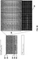
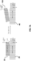
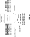
- a multilayer structure 10 useful for understanding the invention and having a plurality of functional layers (FMEDs) 20 is provided in FIG. 1 .
- Functional layers 20 are separated from adjacent functional layers by release layer 30 .
- the plurality of functional layers 20 and release layers 30 are supported on substrate 40 and functional layer 20 is itself a composite of a plurality of layers.
- functional layer 20 may comprise III-V epilayers as illustrated (e.g., p-doped GaAs top layer 21 , a middle layer of low-doped GaAs 22 , and a lower layer of n-doped GaAs 23 ), useful in solar cells.
- the lowest layer is supported on a release layer 30 that is Al 0.9 Ga 0.1 As, that may be doped or undoped. Release layer 30 facilitates access to one or more of functional layers 20 in the multilayer structure 10 .
- release by different kinds of stimuli include: Release by etching, dissolution, burning, etc. (any means of removal) of an embedded sacrificial layer or sacrificial layers (see Table 1 ) .
- the release layer(s) may be selectively etched / dissolved / burned / removed two or more times faster than the FMEDs, and/or masking of structures or layers may be employed to protect the FMEDs from exposure to the agent used for removal of the sacrificial layers.
- the release layer(s) are removed one-at-a-time or two or more sacrificial layers are removed simultaneously.
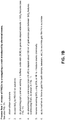
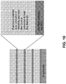
- FIG. 2A illustrates a multilayer structure 10 that is useful for understanding the invention with a mask layer 410 that coats at least a portion of the functional layer 20 , such as between the functional layer 20 and release layer 30 .
- Mask layer 410 optionally comprises an additional mask 400 , such as mask 400 that surrounds the remaining portions not covered by mask 400.
- release layer 30 is labeled as a sacrificial layer and functional layer 20 as FMED having two layers.
- Mask 400 and 410 may act as an etch-stop to protect functional layer 20 from etchent means that removes sacrificial layer 30 , thereby facilitating lift-off of layers 20 from substrate 40 .
- FIG. 2B is a flow-chart that summarizes a process that is useful for understanding the invention for generating transferable FMEDs from a multilayer structure using an encapsulating mask (see also FIG. 2B ).
- FIG. 2C A structure that is useful for understanding the invention and that is useful for use in MESFETs is provided in FIG. 2C , where the functional layer 20 comprises a 120 nm thick GaAs first layer 21 and a 150 nm thick AIGaAs semi-insulating second layer 22 .
- the release layer 30 is a 100 nm thick Al 0.96 Ga 0.04 barrier layer capable of facilitating separation of 30 from substrate 40 .
- EXAMPLE 1 Release of transferable structures for photovoltaics, electronics and LEDs.
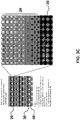
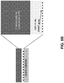
- FIG. 3A-B schematically illustrate methods and structures for simultaneous removal of multiple release layers ( FIG. 3A ) and sequential layer-by-layer removal of release layers ( FIG. 3B ).
- FIG. 3A which illustrates a method that is useful for understanding the invention, a portion of the multilayer structure 10 is exposed to etchant means, thereby forming an etched access passage 35 .
- Passage 35 provides simultaneous access to a plurality of release layers 30 (three, in this example).
- a plurality of transferable structures 100 are available for printing to a surface of interest, such as a device substrate or device component supported by a substrate by any means known in the art (e.g., liquid printing, contact printing, etc.).
- FIG. 3B summarizes layer-by-layer removal, in accordance with a first embodiment of the invention, where etchant access channel 35 spans only the top-most functional layer 20 so that only a single functional layer 20 is released to provide transferable structures 100 from one singly functional layer 20 .
- functional layer 20 may be protected by a mask (not shown) prior to introducing a chemical means for removing release layers 30. The process is repeated for each additional functional layer 20.
- the mother substrate 40 upon which multilayer structure 10 is supported may be reused.
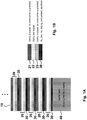
- FIG. 3C-E A number of examples of different functional/release layer compositions and geometry for making different devices or device components are provided in FIG. 3C-E .
- FIG. 3C provides an example of a structure having FMEDs for making photovoltaics, where AIGaAs is the release layer.
- FIG. 3D provides an example of a multilayer structure having FMEDs for making electronics (e.g., MESFETs).
- FIG. 3E provides an example of a multilayer structure having FMEDs for making LEDs.
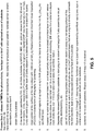
- FIGs 4-5 summarize steps used in a process for releasing multiple functional layers ( FIG. 4 ) or sequential layer-by-layer release of functional layers ( FIG. 5 ).
- Functional layers are released by any means known in the art, such as by undercutting, etching, dissolution, burning, etc. (any means of removal) of an embedded release layer or sacrificial layer.
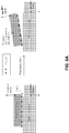
- There are a variety of strategies for releasing functional layers that use a variety of stimuli some are provided in TABLE 1.
- TABLE 1 also shows that the composition of the functional and release layers may be selected depending on the release strategy employed.
- the sacrificial layer(s) are selectively etched / dissolved / burned / removed about two or more times faster than the functional layers that make up the FMEDs.
- a mask layer 400 is provided to protect the FMEDs 20 from exposure to the agent used for removal of the sacrificial layers (see FIG. 2A ).
- release layers are removed one-at-a-time.
- a plurality of release layers may be removed simultaneously (compare FIG. 3A and 3B and flow-charts in FIG. 4 and FIG. 5 .
- FIG. 4 summarizes release of FMEDs for photovoltaics by multiple-layers-at-a-time" with optional re-use of substrate for subsequent generation of additional transferable FMEDS.
- the functional layers comprise epitaxially grown semiconductors.
- the process also works for amorphous or polycrystalline materials similar to the process described in FIG. 12 . Briefly, a GaAs substrate is obtained. Grow epilayers shown in FIG. 3C , for example, on GaAs substrate by MOCVD, MBE, etc. (similar process for FIGs. 3D and 3E for transistors, LEDs, respectively). Pre-treat substrate prior to growth as needed (CMP is optionally required).
- sacrificial layers Grow about -200 nm buffer layer of GaAs adjacent to substrate before depositing or epitaxially growing functional and sacrificial layers.
- a portion of the surface of the top epilayer may be masked with SiO 2 by Plasma-Enhanced Chemical Vapor Deposition (PECVD) and a form of lithography for patterning.
- PECVD Plasma-Enhanced Chemical Vapor Deposition
- the sacrificial layer should not be the one farthest from the substrate (in that case, the release would be in a "one-at-a-time" process as summarized in FIGs 3B and 5 ) .
- a substrate such as a GaAs wafer provides support for growth of epilayers, such as the functional layer described in FIG. 3C , by MOCVD, MBE, etc.
- the substrate may be pre-treated prior to growth as needed (e.g., CMP).
- CMP e.g., CMP
- PECVD Plasma-Enhanced Chemical Vapor Deposition
- the AIGaAs epilayer corresponds to the "mask" 400
- the photoresist encapsulation corresponds to the "additional mask" 410 .
- any of the released FMEDs may be separated from substrate by stamping or do solvent exchange for fluidic assembly or ink jet printing, electrospinning, etc.
- Release is also accomplished by directional etching (e.g. Si 111, Si 110) with a mask layer to protect FMEDs from the etching.
- directional etching e.g. Si 111, Si 110
- EXAMPLE 2 Release of transferable structures by laser ablation.
- FIG. 6A provides a schematic illustration of a laser ablation release method that is useful for understanding the present invention.
- Electromagnetic radiation is introduced through an at least partially transparent substrate 40 upon which functional layer 20 is supported, such as by a laser positioned on the side of substrate 40 that is opposite the surface upon which the multilayer structure rests.
- Laser-induced heating causes release of transferable FMED 100 either by failure of interfacial surface between 20 and 40 or by at least partial removal of a laser-ablating sensitive release surface 30.
- FIG. 6B is an example of a suitable substrate for the release of FMEDs for LEDs by laser ablation.
- Substrate 40 corresponds to a sapphire substrate.
- FIG. 6C summarizes release of FMEDs for LEDs by laser ablation or by ablation/decomposition/chemical reaction that is spontaneous at ambient conditions.
- FIG. 10 summarizes the basic strategy for release of polycrystalline/amorphous FMED materials by selective removal of release layers by different release signals (e.g., electricity and/or heat).
- FIG. 12 summarizes release of amorphous FMED structures by removal of sacrificial layers.
- Example 3 Release of transferable structures by propagation of an induced interfacial crack.
- Another release that is useful for understanding the present invention is by introducing a crack at an interface between FMEDs and the mother substrate and then pulling the FMEDs away from the mother substrate (e.g. using a rubber stamp) to propagate the crack (see FIG. 7A ).
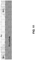
- the crack can be introduced in any number of manners, such as mechanically (e.g. by cutting; see FIGs. 8B-C and 12 ), chemically (e.g. by etching) (see FIGs. 7B and 11 ), or thermally (e.g. by shock induced by thermal expansion coefficient mismatch).
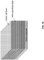
- any of the above means for releasing a transferable structure is combined with a carrier structure, for example a carrier film ( FIG. 8A ), such as a gold film as a carrier structure for printing carbon nanotubes (see Nature Nanotech. Vol 2, p.230 ).
- a carrier structure for example a carrier film ( FIG. 8A ), such as a gold film as a carrier structure for printing carbon nanotubes (see Nature Nanotech. Vol 2, p.230 ).
- This process can be effective for FMEDs that are small (e.g., less than about 50 nm, e.g. molecules, SWNT, etc.) chemically fragile, mechanically fragile, mechanically soft, numerous and/or unwieldy to fabricate individually.
- FIGs 8B and 8C provide examples of a structure and process, respectively, for inducing a crack mechanically between a substrate and a carrier film to release transferable FMEDs.
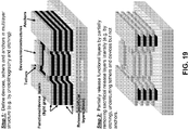
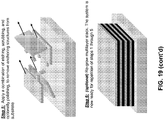
- FIG. 19 is a schematic illustration that is useful for understanding the present invention of partial release of functional layers by partial removal of release layers (sacrificial layers), several release layers at a time (see also FIG. 3A ).
- the release is referred to as "partial" because devices remain tethered to the substrate after the release layers are partially removed. Full release or separation of the devices happens upon their removal, for example, by fracture of tethering structures and retrieval using an elastomer stamp.
- This figure also outlines the steps of removing the anchoring structures to prepare the substrate for re-deposition of multi-layer stacks.
- Some examples of multi-layer structures that may yield printable devices according to the process outlined in FIG. 19 are shown in FIGs 3C-E . The details of the process are outlined in FIG. 4.
- FIG. 4 summarizes release of FMEDs for photovoltaics by "multiple-layers-at-a-time” with optional re-use of substrate for subsequent generation of additional transferable FMEDS.
- the functional layers comprise epitaxially grown semiconductors.
- the process also works for amorphous or polycrystalline materials similar to the process described in FIG. 12 . Briefly, a GaAs substrate is obtained. Grow epilayers shown in FIG. 3C , for example, on GaAs substrate by MOCVD, MBE, etc. (similar process for FIGs. 3D and 3E for transistors, LEDs, respectively). Pre-treat substrate prior to growth as needed (CMP is optionally required).
- sacrificial layers Grow about -200 nm buffer layer of GaAs adjacent to substrate before depositing or epitaxially growing functional and sacrificial layers.
- a portion of the surface of the top epilayer may be masked with SiO 2 by Plasma-Enhanced Chemical Vapor Deposition (PECVD) and a form of lithography for patterning.
- PECVD Plasma-Enhanced Chemical Vapor Deposition
- the sacrificial layer should not be the one farthest from the substrate (in that case, the release would be in a "one-at-a-time" process as summarized in FIGs 3B and 5 ).
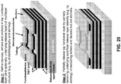
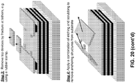
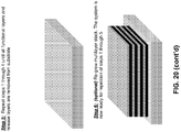
- FIG. 20 is a schematic illustration of partial release of functional layers by partial removal of release layers (sacrificial layer), one release layer at a time in accordance with a second embodiment of the invention (see also FIG. 3B ).
- the release is referred to as "partial” because devices remain tethered to the substrate after the release layers are partially removed. Full release or separation of the devices happens upon their removal, for example, by fracture of tethering structures and retrieval using an elastomer stamp.
- This figure also outlines the steps of removing the anchoring structures to prepare the substrate for repeating the "one-layer-at-a-time release process" (as in FIG. 3B ) and to prepare the substrate for re-deposition of multi-layer stacks.
- FIGs 3C-E Some examples of multi-layer structures that may yield printable devices according to the process outlined herein are shown in FIGs 3C-E .
- the details of the process are outlined in FIG. 5 .
- a substrate such as a GaAs wafer provides support for growth of epilayers, such as the functional layer described in FIG. 3C , by MOCVD, MBE, etc.
- the substrate may be pre-treated prior to growth as needed (e.g., CMP).
- CMP e.g., CMP
- PECVD Plasma-Enhanced Chemical Vapor Deposition
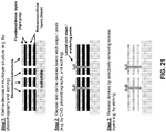
- FIG. 21 is a schematic illustration that is useful for understanding the invention of partial release of functional layers using lateral etch stops or anchoring posts by removing several release layers (sacrificial layers), at a time (see also FIG. 3A ).
- the release is referred to as "partial” because devices remain tethered to the substrate via the lateral etch stops/anchoring posts after the release layers are removed. Full release or separation of the devices happens upon their removal, for example, by fracture of tethering structures and retrieval using an elastomer stamp.
- This figure also outlines the steps of removing the lateral etch stops/anchoring posts to prepare the substrate for re-deposition of multi-layer stacks.
- FIGs 3C-E Some examples of multi-layer structures that may yield printable devices according to the process outlined herein are shown in FIGs 3C-E .
- the details of the process are outlined in the following:
- the functional layers comprise epitaxially grown semiconductors.
- the process also works for amorphous or polycrystalline materials similar to the process described in FIG. 12 . Briefly, a GaAs substrate is obtained. Grow epilayers shown in FIG. 3C , for example, on GaAs substrate by MOCVD, MBE, etc. (similar process for FIGs. 3D and 3E for transistors, LEDs, respectively). Pre-treat substrate prior to growth as needed (CMP is optionally required).
- sacrificial layers Grow about -200 nm buffer layer of GaAs adjacent to substrate before depositing or epitaxially growing functional and sacrificial layers.
- a portion of the surface of the top epilayer may be masked with SiO 2 by Plasma-Enhanced Chemical Vapor Deposition (PECVD) and a form of lithography for patterning.
- PECVD Plasma-Enhanced Chemical Vapor Deposition
- the sacrificial layer should not be the one farthest from the substrate (in that case, the release would be in a "one-at-a-time" process as summarized in FIGs 3B and 5 ).
- a conformal coating of silicon nitride by low-pressure chemical vapor deposition. Pattern the silicon nitride, for example by photolithography and etching using a fluorine plasma, to define lateral etch stops and/or anchoring posts. Expose the substrate to concentrated HF to at least partially remove the exposed sacrificial layers and release the functional epilayers above the sacrificial layers by lateral undercutting. (HF attacks the functional epilayers more slowly (less than 1/10 etch rate) than it does the sacrificial layer). Separate the released FMEDs from substrate by stamping or perform solvent exchange for fluidic assembly or ink jet printing, electrospinning, etc. Use HF to remove any remaining portions of the sacrificial layers.
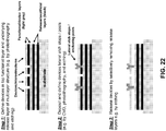
- FIG. 22 schematic illustrations of partial release of functional layers using lateral etch stops or anchoring posts by removing one release layer (sacrificial layer), at a time (see also FIG. 3B ).
- the release is referred to as "partial” because devices remain tethered to the substrate via the lateral etch stops/anchoring posts after the release layers are removed. Full release or separation of the devices happens upon their removal, for example, by fracture of tethering structures and retrieval using an elastomer stamp.
- This figure also outlines the steps of removing the lateral etch stops/anchoring posts for repeating the "one-layer-at-a-time release process" (as in FIG. 3B ) and to prepare the substrate for re-deposition of multi-layer stacks.
- FIGs 3C-E Some examples of multi-layer structures that may yield printable devices according to the process outlined in FIG. 22 are shown in FIGs 3C-E .
- a substrate such as a GaAs wafer provides support for growth of epilayers, such as the functional layer described in FIG. 3C , by MOCVD, MBE, etc.
- the substrate may be pre-treated prior to growth as needed (e.g., CMP).
- CMP e.g., CMP
- PECVD Plasma-Enhanced Chemical Vapor Deposition
- HF HF attacks the functional epilayers more slowly (less than 1/10 etch rate) than it does the sacrificial layer.)
- FIG. 23 schematic useful for understanding the invention of post-release treatment of functional layers with anti-stiction or activation layers after they have been partially released via a process similar to that described in FIG. 20 .
- the anti-stiction or activation layers often self-assembled monolayers (SAMs), serve to avoid adhesion between released layers and underlying layers (anti-stiction) or to promote adhesion (activation) between the released layers and some other entity (e.g. elastomer stamps, nanoparticles, biological entities, etc.).
- SAMs self-assembled monolayers
- FIG. 23 An example of a system to which the process outlined in FIG. 23 may be applied is described in FIG 3D . After the definition of devices (e.g.
- an ethanolic solution of organic thiol-terminated molecule may be used to treat the exposed GaAs surfaces.
- this molecule may be an alkanethiol, for example, hexadecanethiol, or a perfluorinated alkanethiol.
- the thiol may be terminated additionally by reactive chemical groups, for example, octanedithiol.
- FIGs. 35 and 36 provide a further example that is useful for understanding the present invention of an anchoring strategy that further improves generation of transferable structures that break from anchoring structures at well-defined positions, such as by a heterogeneous anchoring strategy (e.g., see FIG. 21 ).
- a heterogeneous anchoring strategy e.g., see FIG. 21 .
- the advantages of the heterogeneous anchoring over homogeneous anchoring, include flexibility in designing breakable tether points, enhanced transfer control, and improvement of transfer registrability.
- various anchoring processes provide more efficient use of the wafer substrate area. Patterned sacrificial regions provide a capability to ensure that the transferable structures break from the anchoring structures at well-defined positions.
- Fig. 36 illustrates the anchoring concept outlined in FIG. 35 and is an example of its practice: printing a mostly-transparent gold mesh from a silicon wafer to plastic.
- FIG. 37 is an SEM of a seven-layer structure, where adjacent GaAs layers are separated by Al 0.9 Ga 0.1 As layers. Epistructures are etched with phosphoric acid and hydrogen peroxide. The multilayer microstructures are machined from epilayers on a GaAs substrate by photolithography and wet etching.
- FIG. 38 is a photograph of the seven GaAs layers retrieved onto PDMS stamps after simultaneous release of the seven GaAs layers. Similar retrieval is expected for individual layer-by-layer release as disclosed herein. Briefly, the release procedure involves masking the epistructure with S1802 photoresist. The masked structure is etched with H 3 PO 4 :H 2 O 2 :DI, 1:13:12, for 1 min. The photoresist is stripped with acetone followed by chemical removal of the release layers with 49%HF for 35 seconds and dry rinsing with N 2 . Layers are sequentially exfoliated (labeled in FIG. 38 as 1 through 8) using PDMS stamps. The 8th stamp is used to check for "left-overs.”
- FIG. 39 provides an optical image of a GaAs layer exfoliated from the multilayer donor substrate on the surface of a PDMS stamp. These layers are ready for printing to device substrate or to a component or a device substrate.
- Example 4 Bulk Quantities of Single-Crystal Silicon Micro-/Nanoribbons Generated from Bulk Wafers.
- This Example that is useful for understanding the present invention demonstrates a strategy for producing bulk quantities of high quality, dimensionally uniform single-crystal silicon micro- and nanoribbons from bulk silicon (111) wafers.
- the process uses etched trenches with controlled rippled structures defined on the sidewalls, together with angled evaporation of masking materials and anisotropic wet etching of the silicon, to produce multilayer stacks of ribbons with uniform thicknesses and lithographically defined lengths and widths, across the entire surface of the wafer. Ribbons with thicknesses between tens and hundreds of nanometers, widths in the micrometer range, and lengths of up to several centimeters, are produced, in bulk quantities, using this approach.
- Printing processes enable the layer by layer transfer of organized arrays of such ribbons to a range of other substrates.
- Good electrical properties (mobilities ⁇ 190 cm 2 V -1 s -1 , on/off >10 4 ) can be achieved with these ribbons in thin film type transistors formed on plastic substrates, thereby demonstrating one potential area of application.
- Nanostructured elements of single-crystal silicon in the form of wires, ribbons, and particles, are of interest for a number of applications in electronics, optoelectronics, sensing, and other areas.
- the ribbon geometry is important for certain devices because it provides, for example, large planar surfaces for chemical sensing and photodetection, and geometries that can efficiently fill the channel regions of transistors. Growth techniques related to the well-developed chemical synthetic approaches used for silicon nanowires 1 have been adapted and applied with some success to produce Si nanoribbons.
- the first disadvantage is irrelevant to the many applications that do not require structures with such small dimensions.
- the second does not, of course, apply to many important materials, including silicon.
- This Example presents results that address the third limitation.
- it introduces a simple method for generating large numbers of high-quality Si ribbons, with thicknesses down to tens of nanometers, from standard bulk Si wafers, in a single processing sequence. Briefly, the approach begins with controlled deep reactive ion etching of silicon wafers through an etch mask to produce trenches with well-defined rippled sidewall morphologies.
- a collimated flux of metal deposited at an angle onto these ripples creates isolated metal lines that act as masks for highly anisotropic wet etching of the silicon along planes parallel to the surface of the wafer.
- This single etching step creates bulk quantities of silicon ribbons in multilayer stacked geometries. These ribbons can be removed from the wafer and solution cast or dry transfer printed onto desired substrates, with or without preserving their lithographically defined spatial order, for integration into devices such as transistors.
- This approach relies only on standard cleanroom processing equipment. As a result, it can be useful to researchers with interest in silicon micro-/nanostructures but without the specialized growth chambers and recipes needed to create them in large quantities using direct synthetic techniques.
- Figure 25 presents a schematic illustration that is useful for understanding the present invention of the fabrication sequence.
- dry thermal oxidation at 1100 °C for 2 h produced a thin (-150 nm) layer of SiO 2 on the surface of the wafer.
- HMDS 1,1,1,3,3,3-hexamethyldidilazane
- PR photoresist
- MF-26A developer contact mode photolithography
- the etching conditions between the deposition cycles define these ripple structures. Because the SF 6 /O 2 mixture gives nearly isotropic etching, the amplitudes and periods of the ripples are related.
- the smallest ripple structure has a period of 80 nm with an amplitude of 50 nm; the largest has a period of 1.5 ⁇ m and an amplitude of 450 nm.
- the etching rate of KOH along the ⁇ 110 ⁇ planes is much faster, by up to several hundred times, than that along the ⁇ 111 ⁇ planes because the ⁇ 110 ⁇ planes have a lower density of atoms and higher density of dangling bonds than the ⁇ 111 ⁇ planes. 14 As a result, this etch proceeded completely from one side of each trench to the adjacent side in a direction parallel to the surface of the wafer, thereby releasing multilayer stacks of individual ribbons with thicknesses determined by the angled evaporation and the ripple structure (i.e., period and amplitude).
- Fig. 26 shows scanning electron microscope (SEM) images of a Si(111) wafer (Montco, Inc., n-type, 1-10 ⁇ cm) at various stages of the process illustrated in Fig. 25 .
- the thicknesses, in the intermediate processing state corresponding to parts g and h of Fig. 26 were 100 ⁇ 10 nm.
- Fully released ribbons had thicknesses of 80 ⁇ 15 nm, due to extended exposure to the KOH etchant.
- the thickness uniformity is excellent in a given multilayer stack, as well as across the wafer, except for the top most ribbon which is somewhat thinner (by -10 nm in this case) than the others due to a slight undercut in the ICPRIE below the SiO 2 mask.
- the lengths and widths of the ribbons are uniform within a variation of ⁇ 120 nm using conventional contact mode photolithography. For this range of thicknesses, widths of 3-5 ⁇ m, and lengths up to several centimeters, the ribbons did not collapse into contact with one another during the KOH etching, until they were completely undercut. By change of the amplitudes and periods of the sidewall ripples, thicknesses between 80 and 300 nm could be achieved, uniformly across the wafer.
- the variations in thicknesses of individual ribbons define the smallest thicknesses that can be achieved reliability. These variations have four main sources. The first two are the roughness on the edges of the SiO 2 masks and on the rippled sidewalls, both of which directly translate into thickness variations.
- lithography e.g., use of electron beam or imprint lithography
- etching e.g., temperature controlled ICPRIE
- deposition e.g., smaller grain sizes in the metal resist lines
- the other limit associated with this process is on the ratio of width to thickness; ratios larger than -60 are difficult to achieve, due to aspects associated with the KOH etching, such as its finite degree of anisotropy as well as mechanical collapse of the ribbons and/or delamination of the metal mask lines before complete undercut.
- Figure 27 shows collections of these ribbons deposited from solution onto a glass slide, after releasing them from the wafer by sonication.
- Experimental data suggest that scaling the process up to as many as 10 layers, with wafers having diameters of up to 150 mm is readily possible. In this case, a single processing sequence ( Figure 25 ) would generate 32 mg of ribbons.
- the optical micrograph of Fig. 28a shows 1.5 ⁇ 10 5 ribbons.
- the scanning electron micrographs highlight the anchors and the etch planes ( Fig. 28b -e ).
- the KOH etch front advances in the ⁇ 110 ⁇ direction, but the front terminates at ⁇ 111 ⁇ planes (i.e., slowest etching plane), as seen in Fig. 28e where the structure tapers into triangular-shaped anchors that meet at a point where two ⁇ 111 ⁇ planes intersect.
- Soft printing processes can transfer these ribbons, one layer at a time, onto other substrates, using the procedures of Fig. 17 .
- the thickness variations arising from previously mentioned factors appear as color variations in the optical image of Fig.
- the atomic force microscopy (AFM) image reveals well-separated steps (or terraces, with heights of up to 10 nm) on the surfaces of the ribbons.
- the surface roughness of areas (1 ⁇ 1 ⁇ m 2 ) that do not include these steps is -0.6 nm, compared to ⁇ 3 nm in similar sized areas that include these steps.
- Similar structures have been observed on the surfaces of Si(111) wafers etched by KOH. 15 Such structures cause some color variations in the optical images.
- the roughness value of 0.6 nm is somewhat larger than that of the top polished surface of the wafer (0.12 nm), of structures generated from a silicon-on-insulator (SOI) substrates (0.18 nm), or of ribbons generated from the top surface of a Si wafer (0.5 nm).
- the roughness originates from the same effects that determine the variations in thickness, as discussed previously. Thickness variations along typical ribbons were ⁇ 15 nm. Variations in the average thicknesses of ribbons in a given array were ⁇ 3 nm.
- Fig. 29c displays four areas of ribbon arrays formed on an ITO-coated PET substrate by four cycles of printing, using a single processed Si wafer.
- the yields on the printed ribbons were 98% for the first layer, 94% for the second layer, 88% for the third layer, and 74% for the fourth layer.
- the lower yield for the fourth layer was mainly due to imperfect transfer from the wafer to the PDMS. Incomplete transfer from an upper layer leaves partially detached ribbons on the wafer that can interfere with subsequent printing cycles.
- field effect transistors Fig. 30a,b
- the transferred Si ribbon arrays sank approximately 35 nm into the SU-8, leaving a residual 100 nm of SU-8 between the bottom surface of the Si ribbons and the SiO 2 gate dielectric, as measured by AFM.
- Thick electrode pads (Ti, 250 nm) defined by photolithography (100 ⁇ m length ⁇ 100 ⁇ m width, spanning 10 Si ribbons) and wet etching with Ti etchant (TFTN, Transene Co.) formed Schottky barrier contacts for the source and drain.
- Ti etchant Ti etchant
- These bottom-gate devices showed n-type enhancement mode gate modulation ( Fig. 30c ,d ), consistent with similar devices formed on SOI wafers using similar processing conditions.
- the transistors exhibited on/off ratios of ⁇ 3 ⁇ 10 4 .
- the linear regime, per ribbon mobilities correspond to 190 cm 2 V -1 s -1 for the first layer and 130 cm 2 V -1 s -1 for the second layer.
- this Example demonstrates a simple fabrication strategy for producing bulk quantities of single-crystal silicon micro-/nanoribbons from bulk silicon (111) wafers.
- Each layer in the multilayer stacks produced by this approach can be separately transfer printed onto other substrates, for integration into devices such as transistors.
- Table 1 Examples of selective etch materials systems Functional material Sacrificial layer Undercut agent Application GaAs, InP, Al x Ga 1-x As (x ⁇ about 50%), InGaAlAsP with composition of AlAs ⁇ about 50%, C, Si, Ge, SiC, SiGe, Au, Ag, Cu, Pd, Pt, assorted multiple layers of above materials (crystalline or amorphous; unsure about amorphous compound semiconductors) Al x Ga 1_x As with x greater than or equal to about 0.7, AlSb, GaSb, SiO 2 Hydrofluoric acid, Hydrofluoric acid vapor, buffered oxide etch LEDs, photovoltaics, electronics (transistors, diodes, etc.), photodiodes, waveguides etc.
- Table 1 Examples of selective etch materials systems Functional material Sacrificial layer Undercut agent Application GaAs, InP, Al x Ga 1-x As (x ⁇ about 50%), InGaAlAsP with composition of AlAs ⁇ about 50%, C
Landscapes
- Engineering & Computer Science (AREA)
- Chemical & Material Sciences (AREA)
- Nanotechnology (AREA)
- Physics & Mathematics (AREA)
- Manufacturing & Machinery (AREA)
- Crystallography & Structural Chemistry (AREA)
- Microelectronics & Electronic Packaging (AREA)
- Condensed Matter Physics & Semiconductors (AREA)
- General Physics & Mathematics (AREA)
- Power Engineering (AREA)
- Computer Hardware Design (AREA)
- Life Sciences & Earth Sciences (AREA)
- Optics & Photonics (AREA)
- Theoretical Computer Science (AREA)
- Mathematical Physics (AREA)
- Biophysics (AREA)
- Thin Film Transistor (AREA)
- Photovoltaic Devices (AREA)
- Sustainable Energy (AREA)
- Recrystallisation Techniques (AREA)
- Weting (AREA)
- Sustainable Development (AREA)
- Led Devices (AREA)
- Electroluminescent Light Sources (AREA)
- Junction Field-Effect Transistors (AREA)
- Light Receiving Elements (AREA)
- Drying Of Semiconductors (AREA)
Applications Claiming Priority (3)
| Application Number | Priority Date | Filing Date | Title |
|---|---|---|---|
| US82635406P | 2006-09-20 | 2006-09-20 | |
| US94465307P | 2007-06-18 | 2007-06-18 | |
| PCT/US2007/079070 WO2008036837A2 (en) | 2006-09-20 | 2007-09-20 | Release strategies for making transferable semiconductor structures, devices and device components |
Publications (3)
| Publication Number | Publication Date |
|---|---|
| EP2064734A2 EP2064734A2 (en) | 2009-06-03 |
| EP2064734A4 EP2064734A4 (en) | 2014-03-26 |
| EP2064734B1 true EP2064734B1 (en) | 2019-01-16 |
Family
ID=39201282
Family Applications (1)
| Application Number | Title | Priority Date | Filing Date |
|---|---|---|---|
| EP07842903.2A Active EP2064734B1 (en) | 2006-09-20 | 2007-09-20 | Method of printing transferable functional structures |
Country Status (8)
| Country | Link |
|---|---|
| US (4) | US7932123B2 (enExample) |
| EP (1) | EP2064734B1 (enExample) |
| JP (3) | JP5319533B2 (enExample) |
| KR (3) | KR101430587B1 (enExample) |
| CN (2) | CN101517700B (enExample) |
| MY (1) | MY149190A (enExample) |
| TW (1) | TWI438827B (enExample) |
| WO (1) | WO2008036837A2 (enExample) |
Families Citing this family (500)
| Publication number | Priority date | Publication date | Assignee | Title |
|---|---|---|---|---|
| US20080055581A1 (en) * | 2004-04-27 | 2008-03-06 | Rogers John A | Devices and methods for pattern generation by ink lithography |
| US8217381B2 (en) | 2004-06-04 | 2012-07-10 | The Board Of Trustees Of The University Of Illinois | Controlled buckling structures in semiconductor interconnects and nanomembranes for stretchable electronics |
| US7521292B2 (en) | 2004-06-04 | 2009-04-21 | The Board Of Trustees Of The University Of Illinois | Stretchable form of single crystal silicon for high performance electronics on rubber substrates |
| CN101120433B (zh) | 2004-06-04 | 2010-12-08 | 伊利诺伊大学评议会 | 用于制造并组装可印刷半导体元件的方法 |
| US7799699B2 (en) | 2004-06-04 | 2010-09-21 | The Board Of Trustees Of The University Of Illinois | Printable semiconductor structures and related methods of making and assembling |
| WO2007083570A1 (ja) * | 2006-01-16 | 2007-07-26 | Matsushita Electric Industrial Co., Ltd. | 半導体小片の製造方法ならびに電界効果トランジスタおよびその製造方法 |
| US20100047959A1 (en) * | 2006-08-07 | 2010-02-25 | Emcore Solar Power, Inc. | Epitaxial Lift Off on Film Mounted Inverted Metamorphic Multijunction Solar Cells |
| KR101430587B1 (ko) | 2006-09-20 | 2014-08-14 | 더 보오드 오브 트러스티스 오브 더 유니버시티 오브 일리노이즈 | 전사가능한 반도체 구조들, 디바이스들 및 디바이스 컴포넌트들을 만들기 위한 릴리스 방안들 |
| US8005402B2 (en) * | 2007-01-10 | 2011-08-23 | Kabushiki Kaisha Toshiba | Charging device, image forming apparatus and charging method |
| CN105826345B (zh) * | 2007-01-17 | 2018-07-31 | 伊利诺伊大学评议会 | 通过基于印刷的组装制造的光学系统 |
| US8097922B1 (en) * | 2007-05-29 | 2012-01-17 | The Regents Of The University Of California | Nanometer-scale transistor architecture providing enhanced carrier mobility |
| WO2009067347A1 (en) * | 2007-11-20 | 2009-05-28 | Arizona Board Of Regents, Acting For And On Behalf Of Arizona State University | Lattice matched multi- junction photovoltaic and optoelectronic devices |
| CN103872002B (zh) | 2008-03-05 | 2017-03-01 | 伊利诺伊大学评议会 | 可拉伸和可折叠的电子器件 |
| US8470701B2 (en) * | 2008-04-03 | 2013-06-25 | Advanced Diamond Technologies, Inc. | Printable, flexible and stretchable diamond for thermal management |
| ES2530458T3 (es) * | 2008-05-12 | 2015-03-03 | Univ Villanova | Células solares y método de fabricación de células solares |
| KR101405023B1 (ko) | 2008-07-04 | 2014-06-10 | 주성엔지니어링(주) | 박막형 태양전지 및 그 제조방법 |
| US7927976B2 (en) * | 2008-07-23 | 2011-04-19 | Semprius, Inc. | Reinforced composite stamp for dry transfer printing of semiconductor elements |
| US7999454B2 (en) * | 2008-08-14 | 2011-08-16 | Global Oled Technology Llc | OLED device with embedded chip driving |
| KR20100027526A (ko) * | 2008-09-02 | 2010-03-11 | 삼성전기주식회사 | 박막 소자 제조방법 |
| US8679888B2 (en) | 2008-09-24 | 2014-03-25 | The Board Of Trustees Of The University Of Illinois | Arrays of ultrathin silicon solar microcells |
| US8097926B2 (en) * | 2008-10-07 | 2012-01-17 | Mc10, Inc. | Systems, methods, and devices having stretchable integrated circuitry for sensing and delivering therapy |
| US8372726B2 (en) | 2008-10-07 | 2013-02-12 | Mc10, Inc. | Methods and applications of non-planar imaging arrays |
| EP2349440B1 (en) | 2008-10-07 | 2019-08-21 | Mc10, Inc. | Catheter balloon having stretchable integrated circuitry and sensor array |
| US8389862B2 (en) | 2008-10-07 | 2013-03-05 | Mc10, Inc. | Extremely stretchable electronics |
| US8886334B2 (en) | 2008-10-07 | 2014-11-11 | Mc10, Inc. | Systems, methods, and devices using stretchable or flexible electronics for medical applications |
| EP2351068B1 (en) * | 2008-11-19 | 2020-11-04 | X Display Company Technology Limited | Printing semiconductor elements by shear-assisted elastomeric stamp transfer |
| JP2010135538A (ja) * | 2008-12-04 | 2010-06-17 | Sumco Corp | 貼り合わせウェーハの製造方法 |
| US8778199B2 (en) | 2009-02-09 | 2014-07-15 | Emoore Solar Power, Inc. | Epitaxial lift off in inverted metamorphic multijunction solar cells |
| MX2011008352A (es) | 2009-02-09 | 2011-11-28 | Semprius Inc | Modulos, receptores y sub-receptores fotovoltaicos tipo concentrador y metodos para formar los mismos. |
| US8409911B2 (en) * | 2009-02-24 | 2013-04-02 | Sunpower Corporation | Methods for metallization of solar cells |
| WO2010111601A2 (en) | 2009-03-26 | 2010-09-30 | Semprius, Inc. | Methods of forming printable integrated circuit devices and devices formed thereby |
| US8754533B2 (en) | 2009-04-14 | 2014-06-17 | Monolithic 3D Inc. | Monolithic three-dimensional semiconductor device and structure |
| US8362482B2 (en) | 2009-04-14 | 2013-01-29 | Monolithic 3D Inc. | Semiconductor device and structure |
| US9577642B2 (en) | 2009-04-14 | 2017-02-21 | Monolithic 3D Inc. | Method to form a 3D semiconductor device |
| US8669778B1 (en) | 2009-04-14 | 2014-03-11 | Monolithic 3D Inc. | Method for design and manufacturing of a 3D semiconductor device |
| US20110199116A1 (en) * | 2010-02-16 | 2011-08-18 | NuPGA Corporation | Method for fabrication of a semiconductor device and structure |
| US8058137B1 (en) | 2009-04-14 | 2011-11-15 | Monolithic 3D Inc. | Method for fabrication of a semiconductor device and structure |
| US9509313B2 (en) | 2009-04-14 | 2016-11-29 | Monolithic 3D Inc. | 3D semiconductor device |
| US8395191B2 (en) | 2009-10-12 | 2013-03-12 | Monolithic 3D Inc. | Semiconductor device and structure |
| EP2427913A4 (en) | 2009-05-04 | 2014-04-30 | Microlink Devices Inc | METHOD OF ASSEMBLING SOLAR CELL ARRAYS AND SOLAR CELLS SHAPED THEREIN |
| US8865489B2 (en) | 2009-05-12 | 2014-10-21 | The Board Of Trustees Of The University Of Illinois | Printed assemblies of ultrathin, microscale inorganic light emitting diodes for deformable and semitransparent displays |
| US8261660B2 (en) * | 2009-07-22 | 2012-09-11 | Semprius, Inc. | Vacuum coupled tool apparatus for dry transfer printing semiconductor elements |
| WO2011034586A2 (en) | 2009-09-16 | 2011-03-24 | Semprius, Inc. | High-yield fabrication of large-format substrates with distributed, independent control elements |
| US9723122B2 (en) | 2009-10-01 | 2017-08-01 | Mc10, Inc. | Protective cases with integrated electronics |
| US8476145B2 (en) | 2010-10-13 | 2013-07-02 | Monolithic 3D Inc. | Method of fabricating a semiconductor device and structure |
| US9099424B1 (en) | 2012-08-10 | 2015-08-04 | Monolithic 3D Inc. | Semiconductor system, device and structure with heat removal |
| US11018133B2 (en) | 2009-10-12 | 2021-05-25 | Monolithic 3D Inc. | 3D integrated circuit |
| US10157909B2 (en) | 2009-10-12 | 2018-12-18 | Monolithic 3D Inc. | 3D semiconductor device and structure |
| US8742476B1 (en) | 2012-11-27 | 2014-06-03 | Monolithic 3D Inc. | Semiconductor device and structure |
| US10043781B2 (en) | 2009-10-12 | 2018-08-07 | Monolithic 3D Inc. | 3D semiconductor device and structure |
| US10366970B2 (en) | 2009-10-12 | 2019-07-30 | Monolithic 3D Inc. | 3D semiconductor device and structure |
| US10388863B2 (en) | 2009-10-12 | 2019-08-20 | Monolithic 3D Inc. | 3D memory device and structure |
| US10354995B2 (en) | 2009-10-12 | 2019-07-16 | Monolithic 3D Inc. | Semiconductor memory device and structure |
| US11374118B2 (en) | 2009-10-12 | 2022-06-28 | Monolithic 3D Inc. | Method to form a 3D integrated circuit |
| US8536023B2 (en) * | 2010-11-22 | 2013-09-17 | Monolithic 3D Inc. | Method of manufacturing a semiconductor device and structure |
| US12027518B1 (en) | 2009-10-12 | 2024-07-02 | Monolithic 3D Inc. | 3D semiconductor devices and structures with metal layers |
| US10910364B2 (en) | 2009-10-12 | 2021-02-02 | Monolitaic 3D Inc. | 3D semiconductor device |
| US8148728B2 (en) | 2009-10-12 | 2012-04-03 | Monolithic 3D, Inc. | Method for fabrication of a semiconductor device and structure |
| US11984445B2 (en) | 2009-10-12 | 2024-05-14 | Monolithic 3D Inc. | 3D semiconductor devices and structures with metal layers |
| WO2011069242A1 (en) * | 2009-12-09 | 2011-06-16 | Cooledge Lighting Inc. | Semiconductor dice transfer-enabling apparatus and method for manufacturing transfer-enabling apparatus |
| EP2513953B1 (en) | 2009-12-16 | 2017-10-18 | The Board of Trustees of the University of Illionis | Electrophysiology using conformal electronics |
| US9936574B2 (en) | 2009-12-16 | 2018-04-03 | The Board Of Trustees Of The University Of Illinois | Waterproof stretchable optoelectronics |
| US10441185B2 (en) | 2009-12-16 | 2019-10-15 | The Board Of Trustees Of The University Of Illinois | Flexible and stretchable electronic systems for epidermal electronics |
| US20110151588A1 (en) * | 2009-12-17 | 2011-06-23 | Cooledge Lighting, Inc. | Method and magnetic transfer stamp for transferring semiconductor dice using magnetic transfer printing techniques |
| US8334152B2 (en) | 2009-12-18 | 2012-12-18 | Cooledge Lighting, Inc. | Method of manufacturing transferable elements incorporating radiation enabled lift off for allowing transfer from host substrate |
| US20110151114A1 (en) * | 2009-12-18 | 2011-06-23 | Cooledge Lighting, Inc. | Composite patterning device and method for removing elements from host substrate by establishing conformal contact between device and a contact surface |
| US8759917B2 (en) * | 2010-01-04 | 2014-06-24 | Samsung Electronics Co., Ltd. | Thin-film transistor having etch stop multi-layer and method of manufacturing the same |
| US8026521B1 (en) | 2010-10-11 | 2011-09-27 | Monolithic 3D Inc. | Semiconductor device and structure |
| US8461035B1 (en) | 2010-09-30 | 2013-06-11 | Monolithic 3D Inc. | Method for fabrication of a semiconductor device and structure |
| US9099526B2 (en) | 2010-02-16 | 2015-08-04 | Monolithic 3D Inc. | Integrated circuit device and structure |
| US8541819B1 (en) | 2010-12-09 | 2013-09-24 | Monolithic 3D Inc. | Semiconductor device and structure |
| US8492886B2 (en) | 2010-02-16 | 2013-07-23 | Monolithic 3D Inc | 3D integrated circuit with logic |
| EP3695792B1 (en) | 2010-03-12 | 2023-06-14 | The Board of Trustees of the University of Illinois | Waterproof stretchable optoelectronics |
| EP2547258B1 (en) | 2010-03-17 | 2015-08-05 | The Board of Trustees of the University of Illionis | Implantable biomedical devices on bioresorbable substrates |
| US9161448B2 (en) | 2010-03-29 | 2015-10-13 | Semprius, Inc. | Laser assisted transfer welding process |
| US9190560B2 (en) | 2010-05-18 | 2015-11-17 | Agency For Science Technology And Research | Method of forming a light emitting diode structure and a light diode structure |
| US8525228B2 (en) * | 2010-07-02 | 2013-09-03 | The Regents Of The University Of California | Semiconductor on insulator (XOI) for high performance field effect transistors |
| US10217667B2 (en) | 2011-06-28 | 2019-02-26 | Monolithic 3D Inc. | 3D semiconductor device, fabrication method and system |
| US9953925B2 (en) | 2011-06-28 | 2018-04-24 | Monolithic 3D Inc. | Semiconductor system and device |
| US8901613B2 (en) | 2011-03-06 | 2014-12-02 | Monolithic 3D Inc. | Semiconductor device and structure for heat removal |
| US9219005B2 (en) | 2011-06-28 | 2015-12-22 | Monolithic 3D Inc. | Semiconductor system and device |
| US8642416B2 (en) | 2010-07-30 | 2014-02-04 | Monolithic 3D Inc. | Method of forming three dimensional integrated circuit devices using layer transfer technique |
| CN104091862B (zh) * | 2010-08-06 | 2017-06-23 | 晶元光电股份有限公司 | 半导体光电元件及其制作方法 |
| WO2012018997A2 (en) * | 2010-08-06 | 2012-02-09 | Semprius, Inc. | Materials and processes for releasing printable compound semiconductor devices |
| US9142468B2 (en) * | 2010-08-26 | 2015-09-22 | Semprius, Inc. | Structures and methods for testing printable integrated circuits |
| US10497713B2 (en) | 2010-11-18 | 2019-12-03 | Monolithic 3D Inc. | 3D semiconductor memory device and structure |
| US8273610B2 (en) | 2010-11-18 | 2012-09-25 | Monolithic 3D Inc. | Method of constructing a semiconductor device and structure |
| US8163581B1 (en) | 2010-10-13 | 2012-04-24 | Monolith IC 3D | Semiconductor and optoelectronic devices |
| US11482440B2 (en) | 2010-12-16 | 2022-10-25 | Monolithic 3D Inc. | 3D semiconductor device and structure with a built-in test circuit for repairing faulty circuits |
| US12362219B2 (en) | 2010-11-18 | 2025-07-15 | Monolithic 3D Inc. | 3D semiconductor memory device and structure |
| US10290682B2 (en) | 2010-10-11 | 2019-05-14 | Monolithic 3D Inc. | 3D IC semiconductor device and structure with stacked memory |
| US11158674B2 (en) | 2010-10-11 | 2021-10-26 | Monolithic 3D Inc. | Method to produce a 3D semiconductor device and structure |
| US11257867B1 (en) | 2010-10-11 | 2022-02-22 | Monolithic 3D Inc. | 3D semiconductor device and structure with oxide bonds |
| US10896931B1 (en) | 2010-10-11 | 2021-01-19 | Monolithic 3D Inc. | 3D semiconductor device and structure |
| US11600667B1 (en) | 2010-10-11 | 2023-03-07 | Monolithic 3D Inc. | Method to produce 3D semiconductor devices and structures with memory |
| US11227897B2 (en) | 2010-10-11 | 2022-01-18 | Monolithic 3D Inc. | Method for producing a 3D semiconductor memory device and structure |
| US11315980B1 (en) | 2010-10-11 | 2022-04-26 | Monolithic 3D Inc. | 3D semiconductor device and structure with transistors |
| US11024673B1 (en) | 2010-10-11 | 2021-06-01 | Monolithic 3D Inc. | 3D semiconductor device and structure |
| US11018191B1 (en) | 2010-10-11 | 2021-05-25 | Monolithic 3D Inc. | 3D semiconductor device and structure |
| US11469271B2 (en) | 2010-10-11 | 2022-10-11 | Monolithic 3D Inc. | Method to produce 3D semiconductor devices and structures with memory |
| US11869915B2 (en) | 2010-10-13 | 2024-01-09 | Monolithic 3D Inc. | Multilevel semiconductor device and structure with image sensors and wafer bonding |
| US11855114B2 (en) | 2010-10-13 | 2023-12-26 | Monolithic 3D Inc. | Multilevel semiconductor device and structure with image sensors and wafer bonding |
| US10998374B1 (en) | 2010-10-13 | 2021-05-04 | Monolithic 3D Inc. | Multilevel semiconductor device and structure |
| US11437368B2 (en) | 2010-10-13 | 2022-09-06 | Monolithic 3D Inc. | Multilevel semiconductor device and structure with oxide bonding |
| US12360310B2 (en) | 2010-10-13 | 2025-07-15 | Monolithic 3D Inc. | Multilevel semiconductor device and structure with oxide bonding |
| US11133344B2 (en) | 2010-10-13 | 2021-09-28 | Monolithic 3D Inc. | Multilevel semiconductor device and structure with image sensors |
| US11984438B2 (en) | 2010-10-13 | 2024-05-14 | Monolithic 3D Inc. | Multilevel semiconductor device and structure with oxide bonding |
| US11043523B1 (en) | 2010-10-13 | 2021-06-22 | Monolithic 3D Inc. | Multilevel semiconductor device and structure with image sensors |
| US11163112B2 (en) | 2010-10-13 | 2021-11-02 | Monolithic 3D Inc. | Multilevel semiconductor device and structure with electromagnetic modulators |
| US11694922B2 (en) | 2010-10-13 | 2023-07-04 | Monolithic 3D Inc. | Multilevel semiconductor device and structure with oxide bonding |
| US11063071B1 (en) | 2010-10-13 | 2021-07-13 | Monolithic 3D Inc. | Multilevel semiconductor device and structure with waveguides |
| US9197804B1 (en) | 2011-10-14 | 2015-11-24 | Monolithic 3D Inc. | Semiconductor and optoelectronic devices |
| US11404466B2 (en) | 2010-10-13 | 2022-08-02 | Monolithic 3D Inc. | Multilevel semiconductor device and structure with image sensors |
| US20120091474A1 (en) * | 2010-10-13 | 2012-04-19 | NuPGA Corporation | Novel semiconductor and optoelectronic devices |
| US10679977B2 (en) | 2010-10-13 | 2020-06-09 | Monolithic 3D Inc. | 3D microdisplay device and structure |
| US10943934B2 (en) | 2010-10-13 | 2021-03-09 | Monolithic 3D Inc. | Multilevel semiconductor device and structure |
| US10978501B1 (en) | 2010-10-13 | 2021-04-13 | Monolithic 3D Inc. | Multilevel semiconductor device and structure with waveguides |
| US11929372B2 (en) | 2010-10-13 | 2024-03-12 | Monolithic 3D Inc. | Multilevel semiconductor device and structure with image sensors and wafer bonding |
| US12080743B2 (en) | 2010-10-13 | 2024-09-03 | Monolithic 3D Inc. | Multilevel semiconductor device and structure with image sensors and wafer bonding |
| US12094892B2 (en) | 2010-10-13 | 2024-09-17 | Monolithic 3D Inc. | 3D micro display device and structure |
| US11605663B2 (en) | 2010-10-13 | 2023-03-14 | Monolithic 3D Inc. | Multilevel semiconductor device and structure with image sensors and wafer bonding |
| US11164898B2 (en) | 2010-10-13 | 2021-11-02 | Monolithic 3D Inc. | Multilevel semiconductor device and structure |
| US11855100B2 (en) | 2010-10-13 | 2023-12-26 | Monolithic 3D Inc. | Multilevel semiconductor device and structure with oxide bonding |
| US11327227B2 (en) | 2010-10-13 | 2022-05-10 | Monolithic 3D Inc. | Multilevel semiconductor device and structure with electromagnetic modulators |
| US10833108B2 (en) | 2010-10-13 | 2020-11-10 | Monolithic 3D Inc. | 3D microdisplay device and structure |
| US12033884B2 (en) | 2010-11-18 | 2024-07-09 | Monolithic 3D Inc. | Methods for producing a 3D semiconductor device and structure with memory cells and multiple metal layers |
| US12144190B2 (en) | 2010-11-18 | 2024-11-12 | Monolithic 3D Inc. | 3D semiconductor device and structure with bonding and memory cells preliminary class |
| US11735462B2 (en) | 2010-11-18 | 2023-08-22 | Monolithic 3D Inc. | 3D semiconductor device and structure with single-crystal layers |
| US12243765B2 (en) | 2010-11-18 | 2025-03-04 | Monolithic 3D Inc. | 3D semiconductor device and structure with metal layers and memory cells |
| US11482439B2 (en) | 2010-11-18 | 2022-10-25 | Monolithic 3D Inc. | Methods for producing a 3D semiconductor memory device comprising charge trap junction-less transistors |
| US11482438B2 (en) | 2010-11-18 | 2022-10-25 | Monolithic 3D Inc. | Methods for producing a 3D semiconductor memory device and structure |
| US11121021B2 (en) | 2010-11-18 | 2021-09-14 | Monolithic 3D Inc. | 3D semiconductor device and structure |
| US11211279B2 (en) | 2010-11-18 | 2021-12-28 | Monolithic 3D Inc. | Method for processing a 3D integrated circuit and structure |
| US12154817B1 (en) | 2010-11-18 | 2024-11-26 | Monolithic 3D Inc. | Methods for producing a 3D semiconductor memory device and structure |
| US12125737B1 (en) | 2010-11-18 | 2024-10-22 | Monolithic 3D Inc. | 3D semiconductor device and structure with metal layers and memory cells |
| US12136562B2 (en) | 2010-11-18 | 2024-11-05 | Monolithic 3D Inc. | 3D semiconductor device and structure with single-crystal layers |
| US11018042B1 (en) | 2010-11-18 | 2021-05-25 | Monolithic 3D Inc. | 3D semiconductor memory device and structure |
| US11355381B2 (en) | 2010-11-18 | 2022-06-07 | Monolithic 3D Inc. | 3D semiconductor memory device and structure |
| US12068187B2 (en) | 2010-11-18 | 2024-08-20 | Monolithic 3D Inc. | 3D semiconductor device and structure with bonding and DRAM memory cells |
| US11107721B2 (en) | 2010-11-18 | 2021-08-31 | Monolithic 3D Inc. | 3D semiconductor device and structure with NAND logic |
| US12272586B2 (en) | 2010-11-18 | 2025-04-08 | Monolithic 3D Inc. | 3D semiconductor memory device and structure with memory and metal layers |
| US11508605B2 (en) | 2010-11-18 | 2022-11-22 | Monolithic 3D Inc. | 3D semiconductor memory device and structure |
| US11854857B1 (en) | 2010-11-18 | 2023-12-26 | Monolithic 3D Inc. | Methods for producing a 3D semiconductor device and structure with memory cells and multiple metal layers |
| US11495484B2 (en) | 2010-11-18 | 2022-11-08 | Monolithic 3D Inc. | 3D semiconductor devices and structures with at least two single-crystal layers |
| US11901210B2 (en) | 2010-11-18 | 2024-02-13 | Monolithic 3D Inc. | 3D semiconductor device and structure with memory |
| US11615977B2 (en) | 2010-11-18 | 2023-03-28 | Monolithic 3D Inc. | 3D semiconductor memory device and structure |
| US11521888B2 (en) | 2010-11-18 | 2022-12-06 | Monolithic 3D Inc. | 3D semiconductor device and structure with high-k metal gate transistors |
| US11031275B2 (en) | 2010-11-18 | 2021-06-08 | Monolithic 3D Inc. | 3D semiconductor device and structure with memory |
| US11862503B2 (en) | 2010-11-18 | 2024-01-02 | Monolithic 3D Inc. | Method for producing a 3D semiconductor device and structure with memory cells and multiple metal layers |
| US11355380B2 (en) | 2010-11-18 | 2022-06-07 | Monolithic 3D Inc. | Methods for producing 3D semiconductor memory device and structure utilizing alignment marks |
| US11569117B2 (en) | 2010-11-18 | 2023-01-31 | Monolithic 3D Inc. | 3D semiconductor device and structure with single-crystal layers |
| US11094576B1 (en) | 2010-11-18 | 2021-08-17 | Monolithic 3D Inc. | Methods for producing a 3D semiconductor memory device and structure |
| US11443971B2 (en) | 2010-11-18 | 2022-09-13 | Monolithic 3D Inc. | 3D semiconductor device and structure with memory |
| US12100611B2 (en) | 2010-11-18 | 2024-09-24 | Monolithic 3D Inc. | Methods for producing a 3D semiconductor device and structure with memory cells and multiple metal layers |
| US11164770B1 (en) | 2010-11-18 | 2021-11-02 | Monolithic 3D Inc. | Method for producing a 3D semiconductor memory device and structure |
| US11784082B2 (en) | 2010-11-18 | 2023-10-10 | Monolithic 3D Inc. | 3D semiconductor device and structure with bonding |
| US11923230B1 (en) | 2010-11-18 | 2024-03-05 | Monolithic 3D Inc. | 3D semiconductor device and structure with bonding |
| US11804396B2 (en) | 2010-11-18 | 2023-10-31 | Monolithic 3D Inc. | Methods for producing a 3D semiconductor device and structure with memory cells and multiple metal layers |
| US11004719B1 (en) | 2010-11-18 | 2021-05-11 | Monolithic 3D Inc. | Methods for producing a 3D semiconductor memory device and structure |
| US11610802B2 (en) | 2010-11-18 | 2023-03-21 | Monolithic 3D Inc. | Method for producing a 3D semiconductor device and structure with single crystal transistors and metal gate electrodes |
| US9899329B2 (en) | 2010-11-23 | 2018-02-20 | X-Celeprint Limited | Interconnection structures and methods for transfer-printed integrated circuit elements with improved interconnection alignment tolerance |
| US12463076B2 (en) | 2010-12-16 | 2025-11-04 | Monolithic 3D Inc. | 3D semiconductor device and structure |
| US9024310B2 (en) | 2011-01-12 | 2015-05-05 | Tsinghua University | Epitaxial structure |
| US8932898B2 (en) | 2011-01-14 | 2015-01-13 | The Board Of Trustees Of The Leland Stanford Junior Univerity | Deposition and post-processing techniques for transparent conductive films |
| US9184319B2 (en) | 2011-01-14 | 2015-11-10 | The Board Of Trustees Of The Leland Stanford Junior University | Multi-terminal multi-junction photovoltaic cells |
| WO2012097163A1 (en) | 2011-01-14 | 2012-07-19 | The Board Of Trustees Of The University Of Illinois | Optical component array having adjustable curvature |
| US8975670B2 (en) | 2011-03-06 | 2015-03-10 | Monolithic 3D Inc. | Semiconductor device and structure for heat removal |
| WO2012158709A1 (en) | 2011-05-16 | 2012-11-22 | The Board Of Trustees Of The University Of Illinois | Thermally managed led arrays assembled by printing |
| US9159635B2 (en) | 2011-05-27 | 2015-10-13 | Mc10, Inc. | Flexible electronic structure |
| WO2012167096A2 (en) | 2011-06-03 | 2012-12-06 | The Board Of Trustees Of The University Of Illinois | Conformable actively multiplexed high-density surface electrode array for brain interfacing |
| US8889485B2 (en) * | 2011-06-08 | 2014-11-18 | Semprius, Inc. | Methods for surface attachment of flipped active componenets |
| CN103748662B (zh) * | 2011-06-28 | 2016-11-09 | 圣戈班晶体及检测公司 | 半导体衬底及形成方法 |
| US10388568B2 (en) | 2011-06-28 | 2019-08-20 | Monolithic 3D Inc. | 3D semiconductor device and system |
| WO2013010113A1 (en) | 2011-07-14 | 2013-01-17 | The Board Of Trustees Of The University Of Illinois | Non-contact transfer printing |
| US9064808B2 (en) * | 2011-07-25 | 2015-06-23 | Synopsys, Inc. | Integrated circuit devices having features with reduced edge curvature and methods for manufacturing the same |
| US20130056044A1 (en) * | 2011-08-03 | 2013-03-07 | Crystal Solar, Inc. | Photovoltaic module fabrication with thin single crystal epitaxial silicon devices |
| US9793144B2 (en) * | 2011-08-30 | 2017-10-17 | Evatec Ag | Wafer holder and temperature conditioning arrangement and method of manufacturing a wafer |
| US8609550B2 (en) * | 2011-09-08 | 2013-12-17 | Synopsys, Inc. | Methods for manufacturing integrated circuit devices having features with reduced edge curvature |
| US9412727B2 (en) | 2011-09-20 | 2016-08-09 | Semprius, Inc. | Printing transferable components using microstructured elastomeric surfaces with pressure modulated reversible adhesion |
| US8492187B2 (en) * | 2011-09-29 | 2013-07-23 | International Business Machines Corporation | High throughput epitaxial liftoff for releasing multiple semiconductor device layers from a single base substrate |
| JP2014532307A (ja) * | 2011-09-30 | 2014-12-04 | マイクロリンク デバイシズ,インコーポレーテッド | エピタキシャルリフトオフによって製造される発光ダイオード |
| US8687399B2 (en) | 2011-10-02 | 2014-04-01 | Monolithic 3D Inc. | Semiconductor device and structure |
| US9029173B2 (en) | 2011-10-18 | 2015-05-12 | Monolithic 3D Inc. | Method for fabrication of a semiconductor device and structure |
| JP5854794B2 (ja) * | 2011-11-25 | 2016-02-09 | キヤノン株式会社 | 有機el装置の製造方法 |
| WO2013089867A2 (en) | 2011-12-01 | 2013-06-20 | The Board Of Trustees Of The University Of Illinois | Transient devices designed to undergo programmable transformations |
| JP5680229B2 (ja) * | 2012-02-07 | 2015-03-04 | 東京応化工業株式会社 | 処理方法及び処理装置 |
| US9000557B2 (en) | 2012-03-17 | 2015-04-07 | Zvi Or-Bach | Semiconductor device and structure |
| EP2830492B1 (en) | 2012-03-30 | 2021-05-19 | The Board of Trustees of the University of Illinois | Appendage mountable electronic devices conformable to surfaces and method of making the same |
| US11164811B2 (en) | 2012-04-09 | 2021-11-02 | Monolithic 3D Inc. | 3D semiconductor device with isolation layers and oxide-to-oxide bonding |
| US11594473B2 (en) | 2012-04-09 | 2023-02-28 | Monolithic 3D Inc. | 3D semiconductor device and structure with metal layers and a connective path |
| US8557632B1 (en) | 2012-04-09 | 2013-10-15 | Monolithic 3D Inc. | Method for fabrication of a semiconductor device and structure |
| US11088050B2 (en) | 2012-04-09 | 2021-08-10 | Monolithic 3D Inc. | 3D semiconductor device with isolation layers |
| US10600888B2 (en) | 2012-04-09 | 2020-03-24 | Monolithic 3D Inc. | 3D semiconductor device |
| US11410912B2 (en) | 2012-04-09 | 2022-08-09 | Monolithic 3D Inc. | 3D semiconductor device with vias and isolation layers |
| US11694944B1 (en) | 2012-04-09 | 2023-07-04 | Monolithic 3D Inc. | 3D semiconductor device and structure with metal layers and a connective path |
| US11476181B1 (en) | 2012-04-09 | 2022-10-18 | Monolithic 3D Inc. | 3D semiconductor device and structure with metal layers |
| US11616004B1 (en) | 2012-04-09 | 2023-03-28 | Monolithic 3D Inc. | 3D semiconductor device and structure with metal layers and a connective path |
| US11881443B2 (en) | 2012-04-09 | 2024-01-23 | Monolithic 3D Inc. | 3D semiconductor device and structure with metal layers and a connective path |
| US11735501B1 (en) | 2012-04-09 | 2023-08-22 | Monolithic 3D Inc. | 3D semiconductor device and structure with metal layers and a connective path |
| KR20130122089A (ko) * | 2012-04-30 | 2013-11-07 | (주)버티클 | 반도체 소자 제조 방법 |
| KR20150038217A (ko) * | 2012-07-24 | 2015-04-08 | 스미또모 가가꾸 가부시키가이샤 | 반도체 기판, 반도체 기판의 제조 방법 및 복합 기판의 제조 방법 |
| KR101878754B1 (ko) | 2012-09-13 | 2018-07-17 | 삼성전자주식회사 | 대면적 갈륨 나이트라이드 기판 제조방법 |
| US8946052B2 (en) | 2012-09-26 | 2015-02-03 | Sandia Corporation | Processes for multi-layer devices utilizing layer transfer |
| US9171794B2 (en) | 2012-10-09 | 2015-10-27 | Mc10, Inc. | Embedding thin chips in polymer |
| EP2731126A1 (en) | 2012-11-09 | 2014-05-14 | Nederlandse Organisatie voor toegepast -natuurwetenschappelijk onderzoek TNO | Method for bonding bare chip dies |
| US8574929B1 (en) | 2012-11-16 | 2013-11-05 | Monolithic 3D Inc. | Method to form a 3D semiconductor device and structure |
| US8686428B1 (en) | 2012-11-16 | 2014-04-01 | Monolithic 3D Inc. | Semiconductor device and structure |
| US11784169B2 (en) | 2012-12-22 | 2023-10-10 | Monolithic 3D Inc. | 3D semiconductor device and structure with metal layers |
| US12051674B2 (en) | 2012-12-22 | 2024-07-30 | Monolithic 3D Inc. | 3D semiconductor device and structure with metal layers |
| US11916045B2 (en) | 2012-12-22 | 2024-02-27 | Monolithic 3D Inc. | 3D semiconductor device and structure with metal layers |
| US11063024B1 (en) | 2012-12-22 | 2021-07-13 | Monlithic 3D Inc. | Method to form a 3D semiconductor device and structure |
| US8674470B1 (en) | 2012-12-22 | 2014-03-18 | Monolithic 3D Inc. | Semiconductor device and structure |
| US11018116B2 (en) | 2012-12-22 | 2021-05-25 | Monolithic 3D Inc. | Method to form a 3D semiconductor device and structure |
| US11217565B2 (en) | 2012-12-22 | 2022-01-04 | Monolithic 3D Inc. | Method to form a 3D semiconductor device and structure |
| US11967583B2 (en) | 2012-12-22 | 2024-04-23 | Monolithic 3D Inc. | 3D semiconductor device and structure with metal layers |
| US11961827B1 (en) | 2012-12-22 | 2024-04-16 | Monolithic 3D Inc. | 3D semiconductor device and structure with metal layers |
| US11309292B2 (en) | 2012-12-22 | 2022-04-19 | Monolithic 3D Inc. | 3D semiconductor device and structure with metal layers |
| KR20140085198A (ko) * | 2012-12-27 | 2014-07-07 | 서울바이오시스 주식회사 | 마스크 패턴을 이용한 기판 분리 방법 및 반도체 소자 제조 방법 |
| US10892169B2 (en) | 2012-12-29 | 2021-01-12 | Monolithic 3D Inc. | 3D semiconductor device and structure |
| US11430668B2 (en) | 2012-12-29 | 2022-08-30 | Monolithic 3D Inc. | 3D semiconductor device and structure with bonding |
| US11177140B2 (en) | 2012-12-29 | 2021-11-16 | Monolithic 3D Inc. | 3D semiconductor device and structure |
| US10115663B2 (en) | 2012-12-29 | 2018-10-30 | Monolithic 3D Inc. | 3D semiconductor device and structure |
| US10600657B2 (en) | 2012-12-29 | 2020-03-24 | Monolithic 3D Inc | 3D semiconductor device and structure |
| US11430667B2 (en) | 2012-12-29 | 2022-08-30 | Monolithic 3D Inc. | 3D semiconductor device and structure with bonding |
| US10903089B1 (en) | 2012-12-29 | 2021-01-26 | Monolithic 3D Inc. | 3D semiconductor device and structure |
| US9385058B1 (en) | 2012-12-29 | 2016-07-05 | Monolithic 3D Inc. | Semiconductor device and structure |
| US12249538B2 (en) | 2012-12-29 | 2025-03-11 | Monolithic 3D Inc. | 3D semiconductor device and structure including power distribution grids |
| US9871034B1 (en) | 2012-12-29 | 2018-01-16 | Monolithic 3D Inc. | Semiconductor device and structure |
| US10651054B2 (en) | 2012-12-29 | 2020-05-12 | Monolithic 3D Inc. | 3D semiconductor device and structure |
| US11004694B1 (en) | 2012-12-29 | 2021-05-11 | Monolithic 3D Inc. | 3D semiconductor device and structure |
| US11087995B1 (en) | 2012-12-29 | 2021-08-10 | Monolithic 3D Inc. | 3D semiconductor device and structure |
| US9613911B2 (en) | 2013-02-06 | 2017-04-04 | The Board Of Trustees Of The University Of Illinois | Self-similar and fractal design for stretchable electronics |
| US10497633B2 (en) | 2013-02-06 | 2019-12-03 | The Board Of Trustees Of The University Of Illinois | Stretchable electronic systems with fluid containment |
| US10840536B2 (en) | 2013-02-06 | 2020-11-17 | The Board Of Trustees Of The University Of Illinois | Stretchable electronic systems with containment chambers |
| WO2014126927A1 (en) | 2013-02-13 | 2014-08-21 | The Board Of Trustees Of The University Of Illinois | Injectable and implantable cellular-scale electronic devices |
| US9875935B2 (en) | 2013-03-08 | 2018-01-23 | Infineon Technologies Austria Ag | Semiconductor device and method for producing the same |
| US9875974B2 (en) | 2013-03-08 | 2018-01-23 | The Board Of Trustees Of The University Of Illinois | Processing techniques for silicon-based transient devices |
| US8902663B1 (en) | 2013-03-11 | 2014-12-02 | Monolithic 3D Inc. | Method of maintaining a memory state |
| US10325651B2 (en) | 2013-03-11 | 2019-06-18 | Monolithic 3D Inc. | 3D semiconductor device with stacked memory |
| US12094965B2 (en) | 2013-03-11 | 2024-09-17 | Monolithic 3D Inc. | 3D semiconductor device and structure with metal layers and memory cells |
| US11935949B1 (en) | 2013-03-11 | 2024-03-19 | Monolithic 3D Inc. | 3D semiconductor device and structure with metal layers and memory cells |
| US11869965B2 (en) | 2013-03-11 | 2024-01-09 | Monolithic 3D Inc. | 3D semiconductor device and structure with metal layers and memory cells |
| US12100646B2 (en) | 2013-03-12 | 2024-09-24 | Monolithic 3D Inc. | 3D semiconductor device and structure with metal layers |
| US10840239B2 (en) | 2014-08-26 | 2020-11-17 | Monolithic 3D Inc. | 3D semiconductor device and structure |
| US11923374B2 (en) | 2013-03-12 | 2024-03-05 | Monolithic 3D Inc. | 3D semiconductor device and structure with metal layers |
| US11398569B2 (en) | 2013-03-12 | 2022-07-26 | Monolithic 3D Inc. | 3D semiconductor device and structure |
| US8994404B1 (en) | 2013-03-12 | 2015-03-31 | Monolithic 3D Inc. | Semiconductor device and structure |
| US11088130B2 (en) | 2014-01-28 | 2021-08-10 | Monolithic 3D Inc. | 3D semiconductor device and structure |
| US10224279B2 (en) | 2013-03-15 | 2019-03-05 | Monolithic 3D Inc. | Semiconductor device and structure |
| WO2014145930A1 (en) * | 2013-03-15 | 2014-09-18 | Amberwave, Inc. | Solar cell |
| US9266717B2 (en) | 2013-03-15 | 2016-02-23 | Versana Micro Inc | Monolithically integrated multi-sensor device on a semiconductor substrate and method therefor |
| US9117749B1 (en) | 2013-03-15 | 2015-08-25 | Monolithic 3D Inc. | Semiconductor device and structure |
| WO2014165686A2 (en) | 2013-04-04 | 2014-10-09 | The Board Of Trustees Of The University Of Illinois | Purification of carbon nanotubes via selective heating |
| US10292263B2 (en) | 2013-04-12 | 2019-05-14 | The Board Of Trustees Of The University Of Illinois | Biodegradable materials for multilayer transient printed circuit boards |
| CA2909313A1 (en) | 2013-04-12 | 2014-10-16 | The Board Of Trustees Of The University Of Illinois | Transient electronic devices comprising inorganic or hybrid inorganic and organic substrates and encapsulates |
| US11341309B1 (en) | 2013-04-15 | 2022-05-24 | Monolithic 3D Inc. | Automation for monolithic 3D devices |
| US11487928B2 (en) | 2013-04-15 | 2022-11-01 | Monolithic 3D Inc. | Automation for monolithic 3D devices |
| US11030371B2 (en) | 2013-04-15 | 2021-06-08 | Monolithic 3D Inc. | Automation for monolithic 3D devices |
| US11720736B2 (en) | 2013-04-15 | 2023-08-08 | Monolithic 3D Inc. | Automation methods for 3D integrated circuits and devices |
| US11574109B1 (en) | 2013-04-15 | 2023-02-07 | Monolithic 3D Inc | Automation methods for 3D integrated circuits and devices |
| US11270055B1 (en) | 2013-04-15 | 2022-03-08 | Monolithic 3D Inc. | Automation for monolithic 3D devices |
| US9021414B1 (en) | 2013-04-15 | 2015-04-28 | Monolithic 3D Inc. | Automation for monolithic 3D devices |
| WO2015006382A1 (en) * | 2013-07-08 | 2015-01-15 | Solexel, Inc. | Thin film solar cell lamination stack for high volume manufacturing |
| WO2015051085A2 (en) | 2013-10-02 | 2015-04-09 | The Board Of Trustees Of The University Of Illinois | Organ mounted electronics |
| WO2015084868A1 (en) | 2013-12-02 | 2015-06-11 | The Regents Of The University Of Michigan | Fabrication of thin-film electronic devices with non-destructive wafer reuse |
| US9058990B1 (en) * | 2013-12-19 | 2015-06-16 | International Business Machines Corporation | Controlled spalling of group III nitrides containing an embedded spall releasing plane |
| JP6570009B2 (ja) * | 2014-01-15 | 2019-09-04 | ザ リージェンツ オブ ザ ユニヴァシティ オブ ミシガン | 印刷法によるエピタキシャルリフトオフ太陽電池の小型放物面型集光器との統合 |
| US12094829B2 (en) | 2014-01-28 | 2024-09-17 | Monolithic 3D Inc. | 3D semiconductor device and structure |
| US11107808B1 (en) | 2014-01-28 | 2021-08-31 | Monolithic 3D Inc. | 3D semiconductor device and structure |
| US11031394B1 (en) | 2014-01-28 | 2021-06-08 | Monolithic 3D Inc. | 3D semiconductor device and structure |
| US10297586B2 (en) | 2015-03-09 | 2019-05-21 | Monolithic 3D Inc. | Methods for processing a 3D semiconductor device |
| US9129863B2 (en) | 2014-02-11 | 2015-09-08 | International Business Machines Corporation | Method to form dual channel group III-V and Si/Ge FINFET CMOS |
| US9123585B1 (en) | 2014-02-11 | 2015-09-01 | International Business Machines Corporation | Method to form group III-V and Si/Ge FINFET on insulator |
| US9236565B2 (en) * | 2014-04-29 | 2016-01-12 | National University Of Singapore | Method for fabricating a magnetoresistive device |
| US9274277B2 (en) | 2014-05-15 | 2016-03-01 | Globalfoundries Inc. | Waveguide devices with supporting anchors |
| US9601356B2 (en) | 2014-06-18 | 2017-03-21 | X-Celeprint Limited | Systems and methods for controlling release of transferable semiconductor structures |
| US9929053B2 (en) | 2014-06-18 | 2018-03-27 | X-Celeprint Limited | Systems and methods for controlling release of transferable semiconductor structures |
| US10050351B2 (en) | 2014-06-18 | 2018-08-14 | X-Celeprint Limited | Multilayer printed capacitors |
| WO2015193436A1 (en) | 2014-06-18 | 2015-12-23 | X-Celeprint Limited | Systems and methods for preparing gan and related materials for micro assembly |
| CN107155373B (zh) | 2014-06-18 | 2019-01-15 | 艾克斯瑟乐普林特有限公司 | 微组装led显示器 |
| US9865600B2 (en) | 2014-06-18 | 2018-01-09 | X-Celeprint Limited | Printed capacitors |
| US20160020131A1 (en) | 2014-07-20 | 2016-01-21 | X-Celeprint Limited | Apparatus and methods for micro-transfer-printing |
| US9111983B1 (en) | 2014-07-31 | 2015-08-18 | Freescale Semiconductor, Inc. | Methods for removing adhesive layers from semiconductor wafers |
| US10736551B2 (en) | 2014-08-11 | 2020-08-11 | The Board Of Trustees Of The University Of Illinois | Epidermal photonic systems and methods |
| WO2016025468A2 (en) | 2014-08-11 | 2016-02-18 | The Board Of Trustees Of The University Of Illinois | Devices and related methods for epidermal characterization of biofluids |
| JP2017532079A (ja) | 2014-08-11 | 2017-11-02 | ザ ボード オブ トラスティーズ オブ ザ ユニヴァーシ | 温度及び熱輸送特性の分析のための表皮デバイス |
| TWI647833B (zh) | 2014-08-26 | 2019-01-11 | X-Celeprint Limited | 微組合複合式顯示裝置及發光元件 |
| US9537069B1 (en) | 2014-09-25 | 2017-01-03 | X-Celeprint Limited | Inorganic light-emitting diode with encapsulating reflector |
| US9799719B2 (en) | 2014-09-25 | 2017-10-24 | X-Celeprint Limited | Active-matrix touchscreen |
| US9799261B2 (en) | 2014-09-25 | 2017-10-24 | X-Celeprint Limited | Self-compensating circuit for faulty display pixels |
| US9991163B2 (en) | 2014-09-25 | 2018-06-05 | X-Celeprint Limited | Small-aperture-ratio display with electrical component |
| US9818725B2 (en) | 2015-06-01 | 2017-11-14 | X-Celeprint Limited | Inorganic-light-emitter display with integrated black matrix |
| US9468050B1 (en) | 2014-09-25 | 2016-10-11 | X-Celeprint Limited | Self-compensating circuit for faulty display pixels |
| US9922956B2 (en) * | 2014-09-26 | 2018-03-20 | Qualcomm Incorporated | Microelectromechanical system (MEMS) bond release structure and method of wafer transfer for three-dimensional integrated circuit (3D IC) integration |
| US10538028B2 (en) | 2014-11-17 | 2020-01-21 | The Board Of Trustees Of The University Of Illinois | Deterministic assembly of complex, three-dimensional architectures by compressive buckling |
| WO2016120398A1 (en) * | 2015-01-30 | 2016-08-04 | Osram Opto Semiconductors Gmbh | Method for producing a semiconductor component and semiconductor component |
| US10340187B2 (en) * | 2015-03-18 | 2019-07-02 | The Regents Of The University Of Michigan | Strain relief epitaxial lift-off via pre-patterned mesas |
| US10825779B2 (en) | 2015-04-19 | 2020-11-03 | Monolithic 3D Inc. | 3D semiconductor device and structure |
| US11056468B1 (en) | 2015-04-19 | 2021-07-06 | Monolithic 3D Inc. | 3D semiconductor device and structure |
| US10381328B2 (en) | 2015-04-19 | 2019-08-13 | Monolithic 3D Inc. | Semiconductor device and structure |
| US11011507B1 (en) | 2015-04-19 | 2021-05-18 | Monolithic 3D Inc. | 3D semiconductor device and structure |
| US9640715B2 (en) | 2015-05-15 | 2017-05-02 | X-Celeprint Limited | Printable inorganic semiconductor structures |
| KR20180033468A (ko) | 2015-06-01 | 2018-04-03 | 더 보드 오브 트러스티즈 오브 더 유니버시티 오브 일리노이 | 무선 전력 및 근거리 통신기능을 갖는 소형화된 전자 시스템 |
| CN107923988A (zh) | 2015-06-01 | 2018-04-17 | 伊利诺伊大学评议会 | Uv感测的替代方法 |
| US9871345B2 (en) | 2015-06-09 | 2018-01-16 | X-Celeprint Limited | Crystalline color-conversion device |
| US10102794B2 (en) | 2015-06-09 | 2018-10-16 | X-Celeprint Limited | Distributed charge-pump power-supply system |
| US11061276B2 (en) | 2015-06-18 | 2021-07-13 | X Display Company Technology Limited | Laser array display |
| US10133426B2 (en) | 2015-06-18 | 2018-11-20 | X-Celeprint Limited | Display with micro-LED front light |
| US9640391B2 (en) * | 2015-06-23 | 2017-05-02 | The Trustees Of The Stevens Institute Of Technology | Direct and pre-patterned synthesis of two-dimensional heterostructures |
| US11160489B2 (en) | 2015-07-02 | 2021-11-02 | The Board Of Trustees Of The University Of Illinois | Wireless optofluidic systems for programmable in vivo pharmacology and optogenetics |
| US9704821B2 (en) | 2015-08-11 | 2017-07-11 | X-Celeprint Limited | Stamp with structured posts |
| US10255834B2 (en) | 2015-07-23 | 2019-04-09 | X-Celeprint Limited | Parallel redundant chiplet system for controlling display pixels |
| US9640108B2 (en) | 2015-08-25 | 2017-05-02 | X-Celeprint Limited | Bit-plane pulse width modulated digital display system |
| US10468363B2 (en) | 2015-08-10 | 2019-11-05 | X-Celeprint Limited | Chiplets with connection posts |
| US11956952B2 (en) | 2015-08-23 | 2024-04-09 | Monolithic 3D Inc. | Semiconductor memory device and structure |
| US10380930B2 (en) | 2015-08-24 | 2019-08-13 | X-Celeprint Limited | Heterogeneous light emitter display system |
| US9899556B2 (en) | 2015-09-14 | 2018-02-20 | Wisconsin Alumni Research Foundation | Hybrid tandem solar cells with improved tunnel junction structures |
| US11937422B2 (en) | 2015-11-07 | 2024-03-19 | Monolithic 3D Inc. | Semiconductor memory device and structure |
| US12100658B2 (en) | 2015-09-21 | 2024-09-24 | Monolithic 3D Inc. | Method to produce a 3D multilayer semiconductor device and structure |
| US11114427B2 (en) | 2015-11-07 | 2021-09-07 | Monolithic 3D Inc. | 3D semiconductor processor and memory device and structure |
| US12250830B2 (en) | 2015-09-21 | 2025-03-11 | Monolithic 3D Inc. | 3D semiconductor memory devices and structures |
| US11978731B2 (en) | 2015-09-21 | 2024-05-07 | Monolithic 3D Inc. | Method to produce a multi-level semiconductor memory device and structure |
| US12477752B2 (en) | 2015-09-21 | 2025-11-18 | Monolithic 3D Inc. | 3D semiconductor memory devices and structures |
| US10515981B2 (en) | 2015-09-21 | 2019-12-24 | Monolithic 3D Inc. | Multilevel semiconductor device and structure with memory |
| US12178055B2 (en) | 2015-09-21 | 2024-12-24 | Monolithic 3D Inc. | 3D semiconductor memory devices and structures |
| US10230048B2 (en) | 2015-09-29 | 2019-03-12 | X-Celeprint Limited | OLEDs for micro transfer printing |
| US10418501B2 (en) | 2015-10-02 | 2019-09-17 | X-Celeprint Limited | Wafer-integrated, ultra-low profile concentrated photovoltaics (CPV) for space applications |
| US10522225B1 (en) | 2015-10-02 | 2019-12-31 | Monolithic 3D Inc. | Semiconductor device with non-volatile memory |
| TWI729414B (zh) * | 2015-10-22 | 2021-06-01 | 愛爾蘭商艾克斯展示公司技術有限公司 | 微型裝置陣列 |
| US12219769B2 (en) | 2015-10-24 | 2025-02-04 | Monolithic 3D Inc. | 3D semiconductor device and structure with logic and memory |
| US11114464B2 (en) | 2015-10-24 | 2021-09-07 | Monolithic 3D Inc. | 3D semiconductor device and structure |
| US10418369B2 (en) | 2015-10-24 | 2019-09-17 | Monolithic 3D Inc. | Multi-level semiconductor memory device and structure |
| US11296115B1 (en) | 2015-10-24 | 2022-04-05 | Monolithic 3D Inc. | 3D semiconductor device and structure |
| US12120880B1 (en) | 2015-10-24 | 2024-10-15 | Monolithic 3D Inc. | 3D semiconductor device and structure with logic and memory |
| US12016181B2 (en) | 2015-10-24 | 2024-06-18 | Monolithic 3D Inc. | 3D semiconductor device and structure with logic and memory |
| US10847540B2 (en) | 2015-10-24 | 2020-11-24 | Monolithic 3D Inc. | 3D semiconductor memory device and structure |
| US11991884B1 (en) | 2015-10-24 | 2024-05-21 | Monolithic 3D Inc. | 3D semiconductor device and structure with logic and memory |
| US12035531B2 (en) | 2015-10-24 | 2024-07-09 | Monolithic 3D Inc. | 3D semiconductor device and structure with logic and memory |
| US10925543B2 (en) | 2015-11-11 | 2021-02-23 | The Board Of Trustees Of The University Of Illinois | Bioresorbable silicon electronics for transient implants |
| US10066819B2 (en) | 2015-12-09 | 2018-09-04 | X-Celeprint Limited | Micro-light-emitting diode backlight system |
| US10091446B2 (en) | 2015-12-23 | 2018-10-02 | X-Celeprint Limited | Active-matrix displays with common pixel control |
| US9930277B2 (en) | 2015-12-23 | 2018-03-27 | X-Celeprint Limited | Serial row-select matrix-addressed system |
| US9786646B2 (en) | 2015-12-23 | 2017-10-10 | X-Celeprint Limited | Matrix addressed device repair |
| US9928771B2 (en) | 2015-12-24 | 2018-03-27 | X-Celeprint Limited | Distributed pulse width modulation control |
| CN105609589B (zh) * | 2016-01-29 | 2017-11-03 | 中国科学院半导体研究所 | 适用于转印的无机半导体薄膜功能单元的制备方法 |
| US11230471B2 (en) | 2016-02-05 | 2022-01-25 | X-Celeprint Limited | Micro-transfer-printed compound sensor device |
| US10361677B2 (en) | 2016-02-18 | 2019-07-23 | X-Celeprint Limited | Transverse bulk acoustic wave filter |
| US10200013B2 (en) | 2016-02-18 | 2019-02-05 | X-Celeprint Limited | Micro-transfer-printed acoustic wave filter device |
| US10109753B2 (en) | 2016-02-19 | 2018-10-23 | X-Celeprint Limited | Compound micro-transfer-printed optical filter device |
| TWI681508B (zh) | 2016-02-25 | 2020-01-01 | 愛爾蘭商艾克斯瑟樂普林特有限公司 | 有效率地微轉印微型裝置於大尺寸基板上 |
| US10193025B2 (en) | 2016-02-29 | 2019-01-29 | X-Celeprint Limited | Inorganic LED pixel structure |
| US10150325B2 (en) | 2016-02-29 | 2018-12-11 | X-Celeprint Limited | Hybrid banknote with electronic indicia |
| US10150326B2 (en) | 2016-02-29 | 2018-12-11 | X-Celeprint Limited | Hybrid document with variable state |
| US9984890B2 (en) * | 2016-03-02 | 2018-05-29 | Tokyo Electron Limited | Isotropic silicon and silicon-germanium etching with tunable selectivity |
| US10153257B2 (en) | 2016-03-03 | 2018-12-11 | X-Celeprint Limited | Micro-printed display |
| US10153256B2 (en) | 2016-03-03 | 2018-12-11 | X-Celeprint Limited | Micro-transfer printable electronic component |
| US10917953B2 (en) | 2016-03-21 | 2021-02-09 | X Display Company Technology Limited | Electrically parallel fused LEDs |
| WO2017173339A1 (en) | 2016-04-01 | 2017-10-05 | The Board Of Trustees Of The University Of Illinois | Implantable medical devices for optogenetics |
| US10103069B2 (en) | 2016-04-01 | 2018-10-16 | X-Celeprint Limited | Pressure-activated electrical interconnection by micro-transfer printing |
| US10199546B2 (en) | 2016-04-05 | 2019-02-05 | X-Celeprint Limited | Color-filter device |
| US10008483B2 (en) | 2016-04-05 | 2018-06-26 | X-Celeprint Limited | Micro-transfer printed LED and color filter structure |
| US9997102B2 (en) | 2016-04-19 | 2018-06-12 | X-Celeprint Limited | Wirelessly powered display and system |
| US10198890B2 (en) | 2016-04-19 | 2019-02-05 | X-Celeprint Limited | Hybrid banknote with electronic indicia using near-field-communications |
| US10360846B2 (en) | 2016-05-10 | 2019-07-23 | X-Celeprint Limited | Distributed pulse-width modulation system with multi-bit digital storage and output device |
| US10622700B2 (en) | 2016-05-18 | 2020-04-14 | X-Celeprint Limited | Antenna with micro-transfer-printed circuit element |
| DE102016109459B4 (de) | 2016-05-23 | 2019-06-13 | X-Fab Semiconductor Foundries Ag | Optimierter Transfer Print (Überführungsdruck) zwischen Trägersubstraten als Verfahren, Trägersubstrat und mikro-technisches Bauelement |
| DE102016109950B3 (de) | 2016-05-30 | 2017-09-28 | X-Fab Semiconductor Foundries Ag | Integrierte Schaltung mit einem - durch einen Überführungsdruck aufgebrachten - Bauelement und Verfahren zur Herstellung der integrierten Schaltung |
| US9997501B2 (en) | 2016-06-01 | 2018-06-12 | X-Celeprint Limited | Micro-transfer-printed light-emitting diode device |
| US10453826B2 (en) | 2016-06-03 | 2019-10-22 | X-Celeprint Limited | Voltage-balanced serial iLED pixel and display |
| US11137641B2 (en) | 2016-06-10 | 2021-10-05 | X Display Company Technology Limited | LED structure with polarized light emission |
| WO2017218878A1 (en) | 2016-06-17 | 2017-12-21 | The Board Of Trustees Of The University Of Illinois | Soft, wearable microfluidic systems capable of capture, storage, and sensing of biofluids |
| US9966301B2 (en) * | 2016-06-27 | 2018-05-08 | New Fab, LLC | Reduced substrate effects in monolithically integrated RF circuits |
| DE102016117030B4 (de) | 2016-07-17 | 2018-07-05 | X-Fab Semiconductor Foundries Ag | Herstellung von Halbleiterstrukturen auf einem Trägersubstrat, die durch Überführungsdruck (Transfer Print) übertragbar sind. |
| US10475876B2 (en) | 2016-07-26 | 2019-11-12 | X-Celeprint Limited | Devices with a single metal layer |
| US10222698B2 (en) | 2016-07-28 | 2019-03-05 | X-Celeprint Limited | Chiplets with wicking posts |
| US11064609B2 (en) | 2016-08-04 | 2021-07-13 | X Display Company Technology Limited | Printable 3D electronic structure |
| US9722134B1 (en) * | 2016-08-16 | 2017-08-01 | Mikro Mesa Technology Co., Ltd. | Method for transferring semiconductor structure |
| US9997399B2 (en) * | 2016-08-16 | 2018-06-12 | Mikro Mesa Technology Co., Ltd. | Method for transferring semiconductor structure |
| US9980341B2 (en) | 2016-09-22 | 2018-05-22 | X-Celeprint Limited | Multi-LED components |
| US10157880B2 (en) | 2016-10-03 | 2018-12-18 | X-Celeprint Limited | Micro-transfer printing with volatile adhesive layer |
| US11869591B2 (en) | 2016-10-10 | 2024-01-09 | Monolithic 3D Inc. | 3D memory devices and structures with control circuits |
| US11812620B2 (en) | 2016-10-10 | 2023-11-07 | Monolithic 3D Inc. | 3D DRAM memory devices and structures with control circuits |
| US11251149B2 (en) | 2016-10-10 | 2022-02-15 | Monolithic 3D Inc. | 3D memory device and structure |
| US11930648B1 (en) | 2016-10-10 | 2024-03-12 | Monolithic 3D Inc. | 3D memory devices and structures with metal layers |
| US11329059B1 (en) | 2016-10-10 | 2022-05-10 | Monolithic 3D Inc. | 3D memory devices and structures with thinned single crystal substrates |
| US12225704B2 (en) | 2016-10-10 | 2025-02-11 | Monolithic 3D Inc. | 3D memory devices and structures with memory arrays and metal layers |
| US11711928B2 (en) | 2016-10-10 | 2023-07-25 | Monolithic 3D Inc. | 3D memory devices and structures with control circuits |
| US10782002B2 (en) | 2016-10-28 | 2020-09-22 | X Display Company Technology Limited | LED optical components |
| WO2018085371A1 (en) * | 2016-11-01 | 2018-05-11 | Massachusetts Institute Of Technology | Lift-off embedded micro and structures |
| US11027462B2 (en) | 2016-11-09 | 2021-06-08 | The Board Of Trustees Of Western Michigan University | Polydimethylsiloxane films and method of manufacture |
| US10347168B2 (en) | 2016-11-10 | 2019-07-09 | X-Celeprint Limited | Spatially dithered high-resolution |
| US10395966B2 (en) | 2016-11-15 | 2019-08-27 | X-Celeprint Limited | Micro-transfer-printable flip-chip structures and methods |
| US10600671B2 (en) | 2016-11-15 | 2020-03-24 | X-Celeprint Limited | Micro-transfer-printable flip-chip structures and methods |
| TWI739949B (zh) | 2016-11-15 | 2021-09-21 | 愛爾蘭商艾克斯展示公司技術有限公司 | 微轉印可印刷覆晶結構及方法 |
| US12042984B2 (en) | 2016-11-17 | 2024-07-23 | Orbotech Ltd. | Hybrid, multi-material 3D printing |
| US10438859B2 (en) | 2016-12-19 | 2019-10-08 | X-Celeprint Limited | Transfer printed device repair |
| US10297502B2 (en) | 2016-12-19 | 2019-05-21 | X-Celeprint Limited | Isolation structure for micro-transfer-printable devices |
| KR101925565B1 (ko) * | 2016-12-30 | 2018-12-06 | (재)한국나노기술원 | 갈라짐 패턴을 이용한 에피층 분리 방법 |
| US10832609B2 (en) * | 2017-01-10 | 2020-11-10 | X Display Company Technology Limited | Digital-drive pulse-width-modulated output system |
| US10332868B2 (en) | 2017-01-26 | 2019-06-25 | X-Celeprint Limited | Stacked pixel structures |
| US10468391B2 (en) | 2017-02-08 | 2019-11-05 | X-Celeprint Limited | Inorganic light-emitting-diode displays with multi-ILED pixels |
| TWI675402B (zh) * | 2017-02-17 | 2019-10-21 | 美商美國亞德諾半導體公司 | 轉印方法及平行轉印方法 |
| US10249739B2 (en) | 2017-03-01 | 2019-04-02 | International Business Machines Corporation | Nanosheet MOSFET with partial release and source/drain epitaxy |
| US10396137B2 (en) | 2017-03-10 | 2019-08-27 | X-Celeprint Limited | Testing transfer-print micro-devices on wafer |
| KR101898858B1 (ko) * | 2017-03-13 | 2018-10-29 | 주식회사 페타룩스 | 태양 전지 |
| US11024608B2 (en) | 2017-03-28 | 2021-06-01 | X Display Company Technology Limited | Structures and methods for electrical connection of micro-devices and substrates |
| DE102017108136B4 (de) | 2017-04-13 | 2019-03-14 | X-Fab Semiconductor Foundries Ag | Geometrisch geformte Bauelemente in einer Anordnung für einen Überführungsdruck (Transfer Print) und zugehörige Verfahren |
| US10468397B2 (en) | 2017-05-05 | 2019-11-05 | X-Celeprint Limited | Matrix addressed tiles and arrays |
| KR102002839B1 (ko) * | 2017-05-23 | 2019-07-23 | 한국기계연구원 | 희생층을 이용한 금속패턴 형성방법 |
| US10777700B2 (en) * | 2017-06-02 | 2020-09-15 | Wisconsin Alumni Research Foundation | Optoelectronic devices based on thin single-crystalline semiconductor films and non-epitaxial optical cavities |
| CN107188115B (zh) * | 2017-06-06 | 2020-05-01 | 北京航空航天大学 | 一种金属/聚合物复合三维微纳米结构的制备方法 |
| US10176991B1 (en) | 2017-07-06 | 2019-01-08 | Wisconsin Alumni Research Foundation | High-quality, single-crystalline silicon-germanium films |
| US10804880B2 (en) | 2018-12-03 | 2020-10-13 | X-Celeprint Limited | Device structures with acoustic wave transducers and connection posts |
| US10943946B2 (en) | 2017-07-21 | 2021-03-09 | X Display Company Technology Limited | iLED displays with substrate holes |
| US10832935B2 (en) | 2017-08-14 | 2020-11-10 | X Display Company Technology Limited | Multi-level micro-device tethers |
| DE102017125217A1 (de) * | 2017-10-27 | 2019-05-02 | Osram Opto Semiconductors Gmbh | Verfahren zur Herstellung von zumindest einem optoelektronischen Bauelement und optoelektronisches Bauelement |
| US10734303B2 (en) * | 2017-11-06 | 2020-08-04 | QROMIS, Inc. | Power and RF devices implemented using an engineered substrate structure |
| US10836200B2 (en) | 2017-11-13 | 2020-11-17 | X Display Company Technology Limited | Rigid micro-modules with ILED and light conductor |
| US20190186041A1 (en) | 2017-12-20 | 2019-06-20 | International Business Machines Corporation | Three-dimensionally stretchable single crystalline semiconductor membrane |
| US10297585B1 (en) | 2017-12-21 | 2019-05-21 | X-Celeprint Limited | Multi-resolution compound micro-devices |
| CN109971373B (zh) * | 2017-12-28 | 2021-01-26 | 清华大学 | 一种粘结方法 |
| IL275961B2 (en) * | 2018-01-23 | 2024-04-01 | Moshe Einav | Voltage-Matched Multi-junction Solar Module Made of 2D Materials |
| US10692996B1 (en) | 2018-02-05 | 2020-06-23 | United States Of America As Represented By The Secretary Of The Air Force | Systems, methods and apparatus for radio frequency devices |
| JP6431631B1 (ja) | 2018-02-28 | 2018-11-28 | 株式会社フィルネックス | 半導体素子の製造方法 |
| TWI670755B (zh) * | 2018-02-28 | 2019-09-01 | 日商菲爾尼克斯股份有限公司 | 半導體元件的製造方法 |
| US11189605B2 (en) | 2018-02-28 | 2021-11-30 | X Display Company Technology Limited | Displays with transparent bezels |
| US10690920B2 (en) | 2018-02-28 | 2020-06-23 | X Display Company Technology Limited | Displays with transparent bezels |
| US10910355B2 (en) | 2018-04-30 | 2021-02-02 | X Display Company Technology Limited | Bezel-free displays |
| US10505079B2 (en) | 2018-05-09 | 2019-12-10 | X-Celeprint Limited | Flexible devices and methods using laser lift-off |
| US11139402B2 (en) | 2018-05-14 | 2021-10-05 | Synopsys, Inc. | Crystal orientation engineering to achieve consistent nanowire shapes |
| US10615574B2 (en) | 2018-05-17 | 2020-04-07 | Wisconsin Alumni Research Foundation | Superlattice heterostructures formed with single crystalline semiconductor nanomembranes and amorphous tunneling barrier layers |
| WO2019232230A1 (en) | 2018-05-30 | 2019-12-05 | The Regents Of The University Of California | Method of removing semiconducting layers from a semiconducting substrate |
| US10832934B2 (en) | 2018-06-14 | 2020-11-10 | X Display Company Technology Limited | Multi-layer tethers for micro-transfer printing |
| US10714001B2 (en) | 2018-07-11 | 2020-07-14 | X Display Company Technology Limited | Micro-light-emitting-diode displays |
| US10796971B2 (en) | 2018-08-13 | 2020-10-06 | X Display Company Technology Limited | Pressure-activated electrical interconnection with additive repair |
| US12236825B2 (en) | 2018-08-13 | 2025-02-25 | X Display Company Technology Limited | Redundant pixel layouts |
| EP4346350B1 (en) | 2018-09-18 | 2025-04-02 | Kabushiki Kaisha Toshiba | Photoelectric conversion device and manufacturing method thereof |
| US10672891B2 (en) * | 2018-10-04 | 2020-06-02 | International Business Machines Corporation | Stacked gate all around MOSFET with symmetric inner spacer formed via sacrificial pure Si anchors |
| US10796938B2 (en) | 2018-10-17 | 2020-10-06 | X Display Company Technology Limited | Micro-transfer printing with selective component removal |
| US10573544B1 (en) | 2018-10-17 | 2020-02-25 | X-Celeprint Limited | Micro-transfer printing with selective component removal |
| US11923472B2 (en) | 2018-11-05 | 2024-03-05 | The United States Of America As Represented By The Secretary Of The Army | Deformable array of semiconductor devices |
| US12162747B2 (en) | 2018-12-03 | 2024-12-10 | X-Celeprint Limited | Enclosed cavity structures |
| US11482979B2 (en) | 2018-12-03 | 2022-10-25 | X Display Company Technology Limited | Printing components over substrate post edges |
| US11528808B2 (en) | 2018-12-03 | 2022-12-13 | X Display Company Technology Limited | Printing components to substrate posts |
| US11274035B2 (en) | 2019-04-24 | 2022-03-15 | X-Celeprint Limited | Overhanging device structures and related methods of manufacture |
| US10790173B2 (en) | 2018-12-03 | 2020-09-29 | X Display Company Technology Limited | Printed components on substrate posts |
| WO2020121649A1 (ja) * | 2018-12-10 | 2020-06-18 | 株式会社フィルネックス | 半導体基板、半導体基板の製造方法及び半導体素子の製造方法 |
| US11282786B2 (en) | 2018-12-12 | 2022-03-22 | X Display Company Technology Limited | Laser-formed interconnects for redundant devices |
| US11114320B2 (en) * | 2018-12-21 | 2021-09-07 | Applied Materials, Inc. | Processing system and method of forming a contact |
| US11483937B2 (en) | 2018-12-28 | 2022-10-25 | X Display Company Technology Limited | Methods of making printed structures |
| US11251139B2 (en) | 2019-01-22 | 2022-02-15 | X-Celeprint Limited | Secure integrated-circuit systems |
| US11322460B2 (en) | 2019-01-22 | 2022-05-03 | X-Celeprint Limited | Secure integrated-circuit systems |
| US10748793B1 (en) | 2019-02-13 | 2020-08-18 | X Display Company Technology Limited | Printing component arrays with different orientations |
| US11088121B2 (en) | 2019-02-13 | 2021-08-10 | X Display Company Technology Limited | Printed LED arrays with large-scale uniformity |
| US11164934B2 (en) | 2019-03-12 | 2021-11-02 | X Display Company Technology Limited | Tiled displays with black-matrix support screens |
| US11094870B2 (en) | 2019-03-12 | 2021-08-17 | X Display Company Technology Limited | Surface-mountable pixel packages and pixel engines |
| DE102019108701A1 (de) * | 2019-04-03 | 2020-10-08 | OSRAM Opto Semiconductors Gesellschaft mit beschränkter Haftung | Verfahren zur Herstellung einer Mehrzahl von Bauteilen, Bauteil und Bauteilverbund aus Bauteilen |
| US11158652B1 (en) | 2019-04-08 | 2021-10-26 | Monolithic 3D Inc. | 3D memory semiconductor devices and structures |
| US10892016B1 (en) | 2019-04-08 | 2021-01-12 | Monolithic 3D Inc. | 3D memory semiconductor devices and structures |
| US11018156B2 (en) | 2019-04-08 | 2021-05-25 | Monolithic 3D Inc. | 3D memory semiconductor devices and structures |
| US11296106B2 (en) | 2019-04-08 | 2022-04-05 | Monolithic 3D Inc. | 3D memory semiconductor devices and structures |
| US11763864B2 (en) | 2019-04-08 | 2023-09-19 | Monolithic 3D Inc. | 3D memory semiconductor devices and structures with bit-line pillars |
| US10714374B1 (en) | 2019-05-09 | 2020-07-14 | X Display Company Technology Limited | High-precision printed structures |
| FR3096172A1 (fr) * | 2019-05-13 | 2020-11-20 | X-Fab France SAS | Transfer Printing for RF Applications |
| US11264458B2 (en) | 2019-05-20 | 2022-03-01 | Synopsys, Inc. | Crystal orientation engineering to achieve consistent nanowire shapes |
| US10944027B2 (en) | 2019-06-14 | 2021-03-09 | X Display Company Technology Limited | Pixel modules with controllers and light emitters |
| US11488943B2 (en) | 2019-06-14 | 2022-11-01 | X Display Company Technology Limited | Modules with integrated circuits and devices |
| KR102687815B1 (ko) * | 2019-06-20 | 2024-07-24 | 엘지전자 주식회사 | 디스플레이 장치 및 반도체 발광소자의 자가조립 방법 |
| DE102019118270B4 (de) | 2019-07-05 | 2021-10-07 | X-Fab Semiconductor Foundries Gmbh | Verfahren zur Herstellung von Halbleiterbauelementen zur Ausbeutesteigerung beim Mikrotransferdruck |
| CN110211880B (zh) * | 2019-07-05 | 2023-04-28 | 苏州汉骅半导体有限公司 | 金刚石基氮化镓hemt结构制造方法 |
| US11101417B2 (en) | 2019-08-06 | 2021-08-24 | X Display Company Technology Limited | Structures and methods for electrically connecting printed components |
| CN110600470B (zh) * | 2019-08-22 | 2021-10-22 | 深圳第三代半导体研究院 | 一种GaN基激光器和AlGaN/GaN HEMT集成器件制备方法 |
| WO2021046269A1 (en) * | 2019-09-04 | 2021-03-11 | Massachusetts Institute Of Technology | Multi-regional epitaxial growth and related systems and articles |
| FI129855B (en) * | 2019-10-08 | 2022-09-30 | Jani Oksanen | METHOD AND STRUCTURE FOR MANUFACTURING THIN FILMS |
| US11637540B2 (en) | 2019-10-30 | 2023-04-25 | X-Celeprint Limited | Non-linear tethers for suspended devices |
| US11127889B2 (en) | 2019-10-30 | 2021-09-21 | X Display Company Technology Limited | Displays with unpatterned layers of light-absorbing material |
| US11626856B2 (en) | 2019-10-30 | 2023-04-11 | X-Celeprint Limited | Non-linear tethers for suspended devices |
| DE102020107288A1 (de) | 2019-12-10 | 2021-06-10 | X-Fab Semiconductor Foundries Gmbh | Halbleiterbauelement und Verfahren zur Herstellung eines Halbleiterbauelements |
| US11062936B1 (en) | 2019-12-19 | 2021-07-13 | X Display Company Technology Limited | Transfer stamps with multiple separate pedestals |
| US11315909B2 (en) | 2019-12-20 | 2022-04-26 | X Display Company Technology Limited | Displays with embedded light emitters |
| WO2021140219A1 (en) | 2020-01-10 | 2021-07-15 | Rockley Photonics Limited | Source wafer and method of preparation thereof |
| US11037912B1 (en) | 2020-01-31 | 2021-06-15 | X Display Company Technology Limited | LED color displays with multiple LEDs connected in series and parallel in different sub-pixels of a pixel |
| US12437174B2 (en) * | 2020-05-01 | 2025-10-07 | X-Celeprint Limited | Hybrid documents with electronic indicia |
| CN111540709A (zh) * | 2020-05-07 | 2020-08-14 | 电子科技大学 | 一种二维半导体器件电路一体化制备的方法 |
| US11538849B2 (en) | 2020-05-28 | 2022-12-27 | X Display Company Technology Limited | Multi-LED structures with reduced circuitry |
| CN116745898A (zh) * | 2020-07-13 | 2023-09-12 | 洛克利光子有限公司 | 用于制备用于微转移印刷的器件试样的方法、包括所述器件试样的器件晶片以及由所述器件晶片制造的光电器件 |
| TWM656434U (zh) * | 2020-09-30 | 2024-06-11 | 日商信越化學工業股份有限公司 | 雷射誘導向前轉移系統、已轉移了光學元件的受體基板的製造系統以及顯示器的製造系統 |
| US11952266B2 (en) | 2020-10-08 | 2024-04-09 | X-Celeprint Limited | Micro-device structures with etch holes |
| US12006205B2 (en) | 2020-10-08 | 2024-06-11 | X-Celeprint Limited | Micro-device structures with etch holes |
| CN112234019B (zh) * | 2020-10-20 | 2023-01-17 | 广东省科学院半导体研究所 | 转移膜、转移组件和微器件曲面转移方法 |
| JP2022073007A (ja) | 2020-10-30 | 2022-05-17 | 信越化学工業株式会社 | 発光ダイオード供給基板の製造方法、発光ダイオードディスプレイの製造方法、発光ダイオードディスプレイの分割ユニットの製造方法、及び素子供給基板の製造方法 |
| US10964899B1 (en) | 2020-11-05 | 2021-03-30 | King Abdulaziz University | Hybrid junction solar light sensitive device |
| KR102774159B1 (ko) | 2021-01-05 | 2025-02-28 | 삼성디스플레이 주식회사 | 표시 장치 및 그 제조 방법 |
| US12074583B2 (en) | 2021-05-11 | 2024-08-27 | X Display Company Technology Limited | Printing components to adhesive substrate posts |
| WO2023015382A1 (en) * | 2021-08-09 | 2023-02-16 | Vuereal Inc. | Selective release of microdevices |
| US12310074B2 (en) * | 2021-11-04 | 2025-05-20 | Taiwan Semiconductor Manufacturing Co., Ltd. | NanoStructure field-effect transistor device and methods of forming |
| US20240421001A1 (en) * | 2021-11-08 | 2024-12-19 | The Board Of Trustees Of The Leland Stanford Junior University | Process for the Pulsed Laser Ejection of Multiple Epitaxial Structures from one Thin Film Growth |
| DE102023102601B4 (de) | 2023-02-02 | 2024-10-17 | X-FAB Global Services GmbH | Halbleiterscheibe und (Mikro-)Transferdruckverfahren |
| CN118737811A (zh) * | 2023-03-28 | 2024-10-01 | 冲电气工业株式会社 | 基板单元的制造方法和基板单元 |
| WO2025036700A1 (en) | 2023-08-16 | 2025-02-20 | Ams-Osram International Gmbh | Method for processing an optoelectronic device and array of optoelectronic devices |
Family Cites Families (104)
| Publication number | Priority date | Publication date | Assignee | Title |
|---|---|---|---|---|
| US5296953A (en) * | 1984-01-23 | 1994-03-22 | Canon Kabushiki Kaisha | Driving method for ferro-electric liquid crystal optical modulation device |
| US4761335A (en) * | 1985-03-07 | 1988-08-02 | National Starch And Chemical Corporation | Alpha-particle protection of semiconductor devices |
| US4784720A (en) | 1985-05-03 | 1988-11-15 | Texas Instruments Incorporated | Trench etch process for a single-wafer RIE dry etch reactor |
| US4855017A (en) * | 1985-05-03 | 1989-08-08 | Texas Instruments Incorporated | Trench etch process for a single-wafer RIE dry etch reactor |
| US4663628A (en) * | 1985-05-06 | 1987-05-05 | Halliburton Company | Method of sampling environmental conditions with a self-contained downhole gauge system |
| US4663828A (en) * | 1985-10-11 | 1987-05-12 | Energy Conversion Devices, Inc. | Process and apparatus for continuous production of lightweight arrays of photovoltaic cells |
| US5107586A (en) * | 1988-09-27 | 1992-04-28 | General Electric Company | Method for interconnecting a stack of integrated circuits at a very high density |
| JPH06118441A (ja) | 1991-11-05 | 1994-04-28 | Tadanobu Kato | 表示セル |
| DE4241045C1 (de) * | 1992-12-05 | 1994-05-26 | Bosch Gmbh Robert | Verfahren zum anisotropen Ätzen von Silicium |
| US5434751A (en) * | 1994-04-11 | 1995-07-18 | Martin Marietta Corporation | Reworkable high density interconnect structure incorporating a release layer |
| US5599616A (en) * | 1994-11-30 | 1997-02-04 | Polaroid Corporation | Laminar imaging medium utilizing cross-linked borated polymeric binder |
| JP4525603B2 (ja) * | 1996-08-27 | 2010-08-18 | セイコーエプソン株式会社 | 薄膜トランジスタの転写方法 |
| US6316283B1 (en) * | 1998-03-25 | 2001-11-13 | Asulab Sa | Batch manufacturing method for photovoltaic cells |
| US6057212A (en) * | 1998-05-04 | 2000-05-02 | International Business Machines Corporation | Method for making bonded metal back-plane substrates |
| KR100434537B1 (ko) * | 1999-03-31 | 2004-06-05 | 삼성전자주식회사 | 다공질 실리콘 혹은 다공질 산화 실리콘을 이용한 두꺼운 희생층을 가진 다층 구조 웨이퍼 및 그 제조방법 |
| JP3657143B2 (ja) * | 1999-04-27 | 2005-06-08 | シャープ株式会社 | 太陽電池及びその製造方法 |
| IL130326A0 (en) * | 1999-06-07 | 2000-06-01 | Yeda Res & Dev | A sensor based on molecular controlled semiconductor resistor |
| US7427526B2 (en) * | 1999-12-20 | 2008-09-23 | The Penn State Research Foundation | Deposited thin films and their use in separation and sacrificial layer applications |
| CA2406214A1 (en) | 2000-04-17 | 2001-10-25 | Stephen J. Fonash | Deposited thin films and their use in separation and sarcrificial layer applications |
| US6787052B1 (en) * | 2000-06-19 | 2004-09-07 | Vladimir Vaganov | Method for fabricating microstructures with deep anisotropic etching of thick silicon wafers |
| US6787750B1 (en) | 2000-06-29 | 2004-09-07 | Siemens Corporate Research, Inc. | Method and apparatus for robust optical tracking with beacon markers |
| US6525352B1 (en) * | 2000-11-22 | 2003-02-25 | Network Photonics, Inc. | Method to reduce release time of micromachined devices |
| US6750480B2 (en) * | 2000-11-27 | 2004-06-15 | Kopin Corporation | Bipolar transistor with lattice matched base layer |
| JP4461616B2 (ja) * | 2000-12-14 | 2010-05-12 | ソニー株式会社 | 素子の転写方法、素子保持基板の形成方法、及び素子保持基板 |
| US6569701B2 (en) * | 2001-10-25 | 2003-05-27 | Rockwell Automation Technologies, Inc. | Method for fabricating an isolated microelectromechanical system device |
| AU2002257289A1 (en) | 2001-05-17 | 2002-11-25 | The Board Of Trustees Of The Leland Stanford Junior University | Device and method for three-dimensional spatial localization and functional interconnection of different types of cells |
| WO2002103760A2 (en) * | 2001-06-14 | 2002-12-27 | Amberware Systems Corporation | Method of selective removal of sige alloys |
| US6917061B2 (en) * | 2001-07-20 | 2005-07-12 | Microlink Devices, Inc. | AlGaAs or InGaP low turn-on voltage GaAs-based heterojunction bipolar transistor |
| US6661037B2 (en) * | 2001-07-20 | 2003-12-09 | Microlink Devices, Inc. | Low emitter resistance contacts to GaAs high speed HBT |
| AU2002322581A1 (en) * | 2001-07-20 | 2003-03-03 | Microlink Devices, Inc. | Graded base gaassb for high speed gaas hbt |
| JP2003077940A (ja) * | 2001-09-06 | 2003-03-14 | Sony Corp | 素子の転写方法及びこれを用いた素子の配列方法、画像表示装置の製造方法 |
| US6936181B2 (en) * | 2001-10-11 | 2005-08-30 | Kovio, Inc. | Methods for patterning using liquid embossing |
| US6864414B2 (en) * | 2001-10-24 | 2005-03-08 | Emcore Corporation | Apparatus and method for integral bypass diode in solar cells |
| ITMO20010248A1 (it) * | 2001-12-12 | 2003-06-12 | Expert System Solutions Srl | Dilatometro ottico perfezionato |
| JP4211256B2 (ja) * | 2001-12-28 | 2009-01-21 | セイコーエプソン株式会社 | 半導体集積回路、半導体集積回路の製造方法、電気光学装置、電子機器 |
| EP1340622B1 (en) * | 2002-03-01 | 2006-12-13 | Dai Nippon Printing Co., Ltd. | Thermally transferable image protective sheet, method for protective layer formation, and record produced by said method |
| JP3889700B2 (ja) * | 2002-03-13 | 2007-03-07 | 三井金属鉱業株式会社 | Cofフィルムキャリアテープの製造方法 |
| JP2003297974A (ja) | 2002-03-29 | 2003-10-17 | Seiko Epson Corp | 半導体装置、電気光学装置および半導体装置の製造方法 |
| US6531331B1 (en) * | 2002-07-16 | 2003-03-11 | Sandia Corporation | Monolithic integration of a MOSFET with a MEMS device |
| US6746890B2 (en) * | 2002-07-17 | 2004-06-08 | Tini Alloy Company | Three dimensional thin film devices and methods of fabrication |
| US6747338B1 (en) | 2002-11-27 | 2004-06-08 | Analog Devices, Inc. | Composite dielectric with improved etch selectivity for high voltage MEMS structures |
| US7494896B2 (en) * | 2003-06-12 | 2009-02-24 | International Business Machines Corporation | Method of forming magnetic random access memory (MRAM) devices on thermally-sensitive substrates using laser transfer |
| US7033961B1 (en) * | 2003-07-15 | 2006-04-25 | Rf Micro Devices, Inc. | Epitaxy/substrate release layer |
| US20050082526A1 (en) * | 2003-10-15 | 2005-04-21 | International Business Machines Corporation | Techniques for layer transfer processing |
| DE10349963A1 (de) * | 2003-10-24 | 2005-06-02 | Leonhard Kurz Gmbh & Co. Kg | Verfahren zur Herstellung einer Folie |
| US7704684B2 (en) * | 2003-12-01 | 2010-04-27 | The Board Of Trustees Of The University Of Illinois | Methods and devices for fabricating three-dimensional nanoscale structures |
| US7018549B2 (en) * | 2003-12-29 | 2006-03-28 | Intel Corporation | Method of fabricating multiple nanowires of uniform length from a single catalytic nanoparticle |
| US8159048B2 (en) * | 2004-01-30 | 2012-04-17 | Triquint Semiconductor, Inc. | Bipolar junction transistor geometry |
| WO2005091370A1 (en) * | 2004-03-22 | 2005-09-29 | Semiconductor Energy Laboratory Co., Ltd. | Method for manufacturing integrated circuit |
| JP5030388B2 (ja) | 2004-03-22 | 2012-09-19 | 株式会社半導体エネルギー研究所 | 薄膜集積回路の作製方法 |
| US7202141B2 (en) * | 2004-03-29 | 2007-04-10 | J.P. Sercel Associates, Inc. | Method of separating layers of material |
| US20080055581A1 (en) | 2004-04-27 | 2008-03-06 | Rogers John A | Devices and methods for pattern generation by ink lithography |
| KR101185613B1 (ko) * | 2004-04-27 | 2012-09-24 | 더 보오드 오브 트러스티스 오브 더 유니버시티 오브 일리노이즈 | 소프트 리소그래피용 복합 패터닝 장치 |
| US8217381B2 (en) | 2004-06-04 | 2012-07-10 | The Board Of Trustees Of The University Of Illinois | Controlled buckling structures in semiconductor interconnects and nanomembranes for stretchable electronics |
| US7943491B2 (en) * | 2004-06-04 | 2011-05-17 | The Board Of Trustees Of The University Of Illinois | Pattern transfer printing by kinetic control of adhesion to an elastomeric stamp |
| US7799699B2 (en) * | 2004-06-04 | 2010-09-21 | The Board Of Trustees Of The University Of Illinois | Printable semiconductor structures and related methods of making and assembling |
| US7521292B2 (en) * | 2004-06-04 | 2009-04-21 | The Board Of Trustees Of The University Of Illinois | Stretchable form of single crystal silicon for high performance electronics on rubber substrates |
| CN101120433B (zh) * | 2004-06-04 | 2010-12-08 | 伊利诺伊大学评议会 | 用于制造并组装可印刷半导体元件的方法 |
| JP4771510B2 (ja) * | 2004-06-23 | 2011-09-14 | キヤノン株式会社 | 半導体層の製造方法及び基板の製造方法 |
| JP4912627B2 (ja) * | 2004-06-24 | 2012-04-11 | 株式会社半導体エネルギー研究所 | 薄膜集積回路の作製方法 |
| US7425523B2 (en) * | 2004-07-05 | 2008-09-16 | Dai Nippon Printing Co., Ltd. | Thermal transfer recording material and thermal transfer recording method |
| US7687886B2 (en) * | 2004-08-19 | 2010-03-30 | Microlink Devices, Inc. | High on-state breakdown heterojunction bipolar transistor |
| DE102005036820A1 (de) * | 2004-08-31 | 2006-03-09 | Osram Opto Semiconductors Gmbh | Strahlungsemittierender Halbleiterkörper für einen vertikal emittierenden Laser und Verfahren zu dessen Herstellung |
| US7259106B2 (en) * | 2004-09-10 | 2007-08-21 | Versatilis Llc | Method of making a microelectronic and/or optoelectronic circuitry sheet |
| US7621044B2 (en) * | 2004-10-22 | 2009-11-24 | Formfactor, Inc. | Method of manufacturing a resilient contact |
| KR100667508B1 (ko) * | 2004-11-08 | 2007-01-10 | 엘지전자 주식회사 | 발광 소자 및 그의 제조방법 |
| US7306963B2 (en) | 2004-11-30 | 2007-12-11 | Spire Corporation | Precision synthesis of quantum dot nanostructures for fluorescent and optoelectronic devices |
| US20060180198A1 (en) * | 2005-02-16 | 2006-08-17 | Sharp Kabushiki Kaisha | Solar cell, solar cell string and method of manufacturing solar cell string |
| JP5052033B2 (ja) * | 2005-04-28 | 2012-10-17 | 株式会社半導体エネルギー研究所 | 半導体装置の作製方法 |
| WO2006130721A2 (en) | 2005-06-02 | 2006-12-07 | The Board Of Trustees Of The University Of Illinois | Printable semiconductor structures and related methods of making and assembling |
| CN102176465B (zh) | 2005-06-02 | 2014-05-07 | 伊利诺伊大学评议会 | 可印刷半导体结构以及相关制造和组装方法 |
| US7462891B2 (en) * | 2005-09-27 | 2008-12-09 | Coldwatt, Inc. | Semiconductor device having an interconnect with sloped walls and method of forming the same |
| US7687707B2 (en) * | 2005-11-16 | 2010-03-30 | Emcore Solar Power, Inc. | Via structures in solar cells with bypass diode |
| WO2007083570A1 (ja) * | 2006-01-16 | 2007-07-26 | Matsushita Electric Industrial Co., Ltd. | 半導体小片の製造方法ならびに電界効果トランジスタおよびその製造方法 |
| EP1991723A2 (en) | 2006-03-03 | 2008-11-19 | The Board Of Trustees Of The University Of Illinois | Methods of making spatially aligned nanotubes and nanotube arrays |
| WO2008030666A2 (en) | 2006-07-25 | 2008-03-13 | The Board Of Trustees Of The University Of Illinois | Multispectral plasmonic crystal sensors |
| DE102006037433B4 (de) * | 2006-08-09 | 2010-08-19 | Ovd Kinegram Ag | Verfahren zur Herstellung eines Mehrschichtkörpers sowie Mehrschichtkörper |
| CN101681695B (zh) | 2006-09-06 | 2013-04-10 | 伊利诺伊大学评议会 | 在用于可拉伸电子元件的半导体互连和纳米膜中的受控弯曲结构 |
| KR101430587B1 (ko) | 2006-09-20 | 2014-08-14 | 더 보오드 오브 트러스티스 오브 더 유니버시티 오브 일리노이즈 | 전사가능한 반도체 구조들, 디바이스들 및 디바이스 컴포넌트들을 만들기 위한 릴리스 방안들 |
| US8742251B2 (en) * | 2006-12-20 | 2014-06-03 | Jds Uniphase Corporation | Multi-segment photovoltaic power converter with a center portion |
| EP2097140B1 (en) | 2006-12-20 | 2012-09-26 | Arkema Inc. | Polymer encapsulation and/or binding |
| CN105826345B (zh) * | 2007-01-17 | 2018-07-31 | 伊利诺伊大学评议会 | 通过基于印刷的组装制造的光学系统 |
| US9508890B2 (en) * | 2007-04-09 | 2016-11-29 | Taiwan Semiconductor Manufacturing Company, Ltd. | Photovoltaics on silicon |
| WO2009011709A1 (en) | 2007-07-19 | 2009-01-22 | The Board Of Trustees Of The University Of Illinois | High resolution electrohydrodynamic jet printing for manufacturing systems |
| CN103872002B (zh) * | 2008-03-05 | 2017-03-01 | 伊利诺伊大学评议会 | 可拉伸和可折叠的电子器件 |
| US8470701B2 (en) * | 2008-04-03 | 2013-06-25 | Advanced Diamond Technologies, Inc. | Printable, flexible and stretchable diamond for thermal management |
| US8946683B2 (en) * | 2008-06-16 | 2015-02-03 | The Board Of Trustees Of The University Of Illinois | Medium scale carbon nanotube thin film integrated circuits on flexible plastic substrates |
| US8679888B2 (en) | 2008-09-24 | 2014-03-25 | The Board Of Trustees Of The University Of Illinois | Arrays of ultrathin silicon solar microcells |
| KR20110099029A (ko) * | 2008-12-08 | 2011-09-05 | 알타 디바이씨즈, 인크. | 에피택셜 리프트 오프를 위한 다중 스택 증착 |
| KR101046064B1 (ko) | 2008-12-11 | 2011-07-01 | 삼성전기주식회사 | 박막소자 제조방법 |
| US8865489B2 (en) * | 2009-05-12 | 2014-10-21 | The Board Of Trustees Of The University Of Illinois | Printed assemblies of ultrathin, microscale inorganic light emitting diodes for deformable and semitransparent displays |
| US10441185B2 (en) | 2009-12-16 | 2019-10-15 | The Board Of Trustees Of The University Of Illinois | Flexible and stretchable electronic systems for epidermal electronics |
| EP2513953B1 (en) | 2009-12-16 | 2017-10-18 | The Board of Trustees of the University of Illionis | Electrophysiology using conformal electronics |
| US9936574B2 (en) | 2009-12-16 | 2018-04-03 | The Board Of Trustees Of The University Of Illinois | Waterproof stretchable optoelectronics |
| US9057994B2 (en) * | 2010-01-08 | 2015-06-16 | The Board Of Trustees Of The University Of Illinois | High resolution printing of charge |
| EP2547258B1 (en) * | 2010-03-17 | 2015-08-05 | The Board of Trustees of the University of Illionis | Implantable biomedical devices on bioresorbable substrates |
| US8562095B2 (en) | 2010-11-01 | 2013-10-22 | The Board Of Trustees Of The University Of Illinois | High resolution sensing and control of electrohydrodynamic jet printing |
| WO2012097163A1 (en) | 2011-01-14 | 2012-07-19 | The Board Of Trustees Of The University Of Illinois | Optical component array having adjustable curvature |
| WO2012158709A1 (en) | 2011-05-16 | 2012-11-22 | The Board Of Trustees Of The University Of Illinois | Thermally managed led arrays assembled by printing |
| WO2012167096A2 (en) | 2011-06-03 | 2012-12-06 | The Board Of Trustees Of The University Of Illinois | Conformable actively multiplexed high-density surface electrode array for brain interfacing |
| WO2013010113A1 (en) | 2011-07-14 | 2013-01-17 | The Board Of Trustees Of The University Of Illinois | Non-contact transfer printing |
| WO2013089867A2 (en) | 2011-12-01 | 2013-06-20 | The Board Of Trustees Of The University Of Illinois | Transient devices designed to undergo programmable transformations |
| EP2830492B1 (en) | 2012-03-30 | 2021-05-19 | The Board of Trustees of the University of Illinois | Appendage mountable electronic devices conformable to surfaces and method of making the same |
| US10497633B2 (en) | 2013-02-06 | 2019-12-03 | The Board Of Trustees Of The University Of Illinois | Stretchable electronic systems with fluid containment |
-
2007
- 2007-09-20 KR KR1020097007923A patent/KR101430587B1/ko active Active
- 2007-09-20 TW TW096135244A patent/TWI438827B/zh active
- 2007-09-20 KR KR1020147001286A patent/KR101615255B1/ko active Active
- 2007-09-20 CN CN200780034881.7A patent/CN101517700B/zh active Active
- 2007-09-20 EP EP07842903.2A patent/EP2064734B1/en active Active
- 2007-09-20 US US11/858,788 patent/US7932123B2/en active Active
- 2007-09-20 CN CN201410111306.4A patent/CN103956336B/zh active Active
- 2007-09-20 MY MYPI20090715A patent/MY149190A/en unknown
- 2007-09-20 JP JP2009529401A patent/JP5319533B2/ja active Active
- 2007-09-20 WO PCT/US2007/079070 patent/WO2008036837A2/en not_active Ceased
- 2007-09-20 KR KR1020147029075A patent/KR101588019B1/ko active Active
-
2011
- 2011-03-24 US US13/071,027 patent/US8895406B2/en active Active
- 2011-09-08 US US13/228,041 patent/US20110316120A1/en not_active Abandoned
-
2013
- 2013-07-10 JP JP2013144886A patent/JP5805712B2/ja active Active
-
2014
- 2014-04-07 US US14/246,962 patent/US9349900B2/en active Active
-
2015
- 2015-09-02 JP JP2015172848A patent/JP6238141B2/ja active Active
Non-Patent Citations (1)
| Title |
|---|
| None * |
Also Published As
| Publication number | Publication date |
|---|---|
| JP2010504649A (ja) | 2010-02-12 |
| TWI438827B (zh) | 2014-05-21 |
| KR101615255B1 (ko) | 2016-05-11 |
| JP2016040828A (ja) | 2016-03-24 |
| JP6238141B2 (ja) | 2017-11-29 |
| JP5319533B2 (ja) | 2013-10-16 |
| JP2013247372A (ja) | 2013-12-09 |
| WO2008036837A2 (en) | 2008-03-27 |
| US20140361409A1 (en) | 2014-12-11 |
| MY149190A (en) | 2013-07-31 |
| KR101588019B1 (ko) | 2016-02-12 |
| CN103956336B (zh) | 2019-08-16 |
| KR20140016432A (ko) | 2014-02-07 |
| US20110171813A1 (en) | 2011-07-14 |
| CN101517700A (zh) | 2009-08-26 |
| CN101517700B (zh) | 2014-04-16 |
| WO2008036837A3 (en) | 2009-05-14 |
| US20080108171A1 (en) | 2008-05-08 |
| EP2064734A2 (en) | 2009-06-03 |
| EP2064734A4 (en) | 2014-03-26 |
| JP5805712B2 (ja) | 2015-11-04 |
| TW200832513A (en) | 2008-08-01 |
| CN103956336A (zh) | 2014-07-30 |
| KR20140141662A (ko) | 2014-12-10 |
| US9349900B2 (en) | 2016-05-24 |
| KR101430587B1 (ko) | 2014-08-14 |
| KR20090078803A (ko) | 2009-07-20 |
| US7932123B2 (en) | 2011-04-26 |
| US8895406B2 (en) | 2014-11-25 |
| US20110316120A1 (en) | 2011-12-29 |
Similar Documents
| Publication | Publication Date | Title |
|---|---|---|
| EP2064734B1 (en) | Method of printing transferable functional structures | |
| CN103155114B (zh) | 用于释放可印刷化合物半导体器件的材料和过程 | |
| TWI427802B (zh) | 可印刷半導體結構及製造和組合之相關方法 | |
| KR102087337B1 (ko) | 인장 가능한 가요성 장치의 제조 방법 | |
| US7947548B2 (en) | Multifunctional tape | |
| TW201225171A (en) | Method of manufacturing a semiconductor device | |
| EP4035201A1 (en) | Composition of matter | |
| Maeda et al. | Thin epitaxial film of Ge and III-V directly bonded onto Si substrate | |
| JP7787804B2 (ja) | ナノワイヤデバイス | |
| Guan et al. | Flexible Light‐Emitting Diodes Based on Inorganic Semiconductor Nanostructures: From Thin Films to Nanowires |
Legal Events
| Date | Code | Title | Description |
|---|---|---|---|
| PUAI | Public reference made under article 153(3) epc to a published international application that has entered the european phase |
Free format text: ORIGINAL CODE: 0009012 |
|
| 17P | Request for examination filed |
Effective date: 20090326 |
|
| AK | Designated contracting states |
Kind code of ref document: A2 Designated state(s): AT BE BG CH CY CZ DE DK EE ES FI FR GB GR HU IE IS IT LI LT LU LV MC MT NL PL PT RO SE SI SK TR |
|
| AX | Request for extension of the european patent |
Extension state: AL BA HR MK RS |
|
| R17D | Deferred search report published (corrected) |
Effective date: 20090514 |
|
| RIC1 | Information provided on ipc code assigned before grant |
Ipc: H01L 21/30 20060101ALI20090525BHEP Ipc: H01L 21/00 20060101AFI20090525BHEP |
|
| RIN1 | Information on inventor provided before grant (corrected) |
Inventor name: YOON, JONGSEUNG Inventor name: MEITL, MATTHEW Inventor name: KO, HEUNG CHO Inventor name: NUZZO, RALPH G. Inventor name: BACA, ALFRED J. Inventor name: ROGERS, JOHN A. Inventor name: MENARD, ETIENNE |
|
| DAX | Request for extension of the european patent (deleted) | ||
| A4 | Supplementary search report drawn up and despatched |
Effective date: 20140224 |
|
| RIC1 | Information provided on ipc code assigned before grant |
Ipc: H01L 31/072 20120101ALI20140218BHEP Ipc: B82Y 10/00 20110101ALI20140218BHEP Ipc: H01L 21/78 20060101ALI20140218BHEP Ipc: H01L 31/0687 20120101ALI20140218BHEP Ipc: B82Y 20/00 20110101ALI20140218BHEP Ipc: H01L 29/20 20060101AFI20140218BHEP Ipc: B81C 1/00 20060101ALI20140218BHEP |
|
| 17Q | First examination report despatched |
Effective date: 20160523 |
|
| STAA | Information on the status of an ep patent application or granted ep patent |
Free format text: STATUS: EXAMINATION IS IN PROGRESS |
|
| REG | Reference to a national code |
Ref country code: DE Ref legal event code: R079 Ref document number: 602007057456 Country of ref document: DE Free format text: PREVIOUS MAIN CLASS: H01L0021280000 Ipc: H01L0029200000 |
|
| GRAP | Despatch of communication of intention to grant a patent |
Free format text: ORIGINAL CODE: EPIDOSNIGR1 |
|
| STAA | Information on the status of an ep patent application or granted ep patent |
Free format text: STATUS: GRANT OF PATENT IS INTENDED |
|
| RIC1 | Information provided on ipc code assigned before grant |
Ipc: H01L 31/0304 20060101ALN20180725BHEP Ipc: H01L 31/068 20060101ALI20180725BHEP Ipc: B82Y 20/00 20110101ALI20180725BHEP Ipc: H01L 31/0735 20120101ALN20180725BHEP Ipc: H01L 21/78 20060101ALI20180725BHEP Ipc: B81C 1/00 20060101ALI20180725BHEP Ipc: H01L 31/072 20060101ALI20180725BHEP Ipc: B82Y 10/00 20110101ALI20180725BHEP Ipc: B82Y 40/00 20110101ALI20180725BHEP Ipc: H01L 29/20 20060101AFI20180725BHEP Ipc: H01L 31/0725 20120101ALN20180725BHEP Ipc: H01L 29/15 20060101ALI20180725BHEP Ipc: H01L 31/0687 20120101ALI20180725BHEP Ipc: H01L 31/18 20060101ALN20180725BHEP |
|
| INTG | Intention to grant announced |
Effective date: 20180808 |
|
| RIC1 | Information provided on ipc code assigned before grant |
Ipc: B82Y 20/00 20110101ALI20180727BHEP Ipc: B82Y 40/00 20110101ALI20180727BHEP Ipc: H01L 31/068 20060101ALI20180727BHEP Ipc: H01L 31/0725 20120101ALN20180727BHEP Ipc: H01L 31/0687 20120101ALI20180727BHEP Ipc: H01L 29/20 20060101AFI20180727BHEP Ipc: H01L 31/0304 20060101ALN20180727BHEP Ipc: B81C 1/00 20060101ALI20180727BHEP Ipc: H01L 31/072 20060101ALI20180727BHEP Ipc: H01L 31/0735 20120101ALN20180727BHEP Ipc: H01L 31/18 20060101ALN20180727BHEP Ipc: H01L 29/15 20060101ALI20180727BHEP Ipc: B82Y 10/00 20110101ALI20180727BHEP Ipc: H01L 21/78 20060101ALI20180727BHEP |
|
| RIN1 | Information on inventor provided before grant (corrected) |
Inventor name: ROGERS, JOHN A. Inventor name: BACA, ALFRED J. Inventor name: YOON, JONGSEUNG Inventor name: KO, HEUNG CHO Inventor name: MENARD, ETIENNE Inventor name: MEITL, MATTHEW Inventor name: NUZZO, RALPH G. |
|
| GRAS | Grant fee paid |
Free format text: ORIGINAL CODE: EPIDOSNIGR3 |
|
| GRAA | (expected) grant |
Free format text: ORIGINAL CODE: 0009210 |
|
| STAA | Information on the status of an ep patent application or granted ep patent |
Free format text: STATUS: THE PATENT HAS BEEN GRANTED |
|
| AK | Designated contracting states |
Kind code of ref document: B1 Designated state(s): AT BE BG CH CY CZ DE DK EE ES FI FR GB GR HU IE IS IT LI LT LU LV MC MT NL PL PT RO SE SI SK TR |
|
| REG | Reference to a national code |
Ref country code: GB Ref legal event code: FG4D |
|
| REG | Reference to a national code |
Ref country code: CH Ref legal event code: EP |
|
| REG | Reference to a national code |
Ref country code: IE Ref legal event code: FG4D |
|
| REG | Reference to a national code |
Ref country code: DE Ref legal event code: R096 Ref document number: 602007057456 Country of ref document: DE |
|
| REG | Reference to a national code |
Ref country code: AT Ref legal event code: REF Ref document number: 1090359 Country of ref document: AT Kind code of ref document: T Effective date: 20190215 |
|
| REG | Reference to a national code |
Ref country code: NL Ref legal event code: MP Effective date: 20190116 |
|
| REG | Reference to a national code |
Ref country code: LT Ref legal event code: MG4D |
|
| PG25 | Lapsed in a contracting state [announced via postgrant information from national office to epo] |
Ref country code: NL Free format text: LAPSE BECAUSE OF FAILURE TO SUBMIT A TRANSLATION OF THE DESCRIPTION OR TO PAY THE FEE WITHIN THE PRESCRIBED TIME-LIMIT Effective date: 20190116 |
|
| REG | Reference to a national code |
Ref country code: AT Ref legal event code: MK05 Ref document number: 1090359 Country of ref document: AT Kind code of ref document: T Effective date: 20190116 |
|
| PG25 | Lapsed in a contracting state [announced via postgrant information from national office to epo] |
Ref country code: ES Free format text: LAPSE BECAUSE OF FAILURE TO SUBMIT A TRANSLATION OF THE DESCRIPTION OR TO PAY THE FEE WITHIN THE PRESCRIBED TIME-LIMIT Effective date: 20190116 Ref country code: LT Free format text: LAPSE BECAUSE OF FAILURE TO SUBMIT A TRANSLATION OF THE DESCRIPTION OR TO PAY THE FEE WITHIN THE PRESCRIBED TIME-LIMIT Effective date: 20190116 Ref country code: PL Free format text: LAPSE BECAUSE OF FAILURE TO SUBMIT A TRANSLATION OF THE DESCRIPTION OR TO PAY THE FEE WITHIN THE PRESCRIBED TIME-LIMIT Effective date: 20190116 Ref country code: FI Free format text: LAPSE BECAUSE OF FAILURE TO SUBMIT A TRANSLATION OF THE DESCRIPTION OR TO PAY THE FEE WITHIN THE PRESCRIBED TIME-LIMIT Effective date: 20190116 Ref country code: PT Free format text: LAPSE BECAUSE OF FAILURE TO SUBMIT A TRANSLATION OF THE DESCRIPTION OR TO PAY THE FEE WITHIN THE PRESCRIBED TIME-LIMIT Effective date: 20190516 Ref country code: SE Free format text: LAPSE BECAUSE OF FAILURE TO SUBMIT A TRANSLATION OF THE DESCRIPTION OR TO PAY THE FEE WITHIN THE PRESCRIBED TIME-LIMIT Effective date: 20190116 |
|
| PG25 | Lapsed in a contracting state [announced via postgrant information from national office to epo] |
Ref country code: BG Free format text: LAPSE BECAUSE OF FAILURE TO SUBMIT A TRANSLATION OF THE DESCRIPTION OR TO PAY THE FEE WITHIN THE PRESCRIBED TIME-LIMIT Effective date: 20190416 Ref country code: GR Free format text: LAPSE BECAUSE OF FAILURE TO SUBMIT A TRANSLATION OF THE DESCRIPTION OR TO PAY THE FEE WITHIN THE PRESCRIBED TIME-LIMIT Effective date: 20190417 Ref country code: IS Free format text: LAPSE BECAUSE OF FAILURE TO SUBMIT A TRANSLATION OF THE DESCRIPTION OR TO PAY THE FEE WITHIN THE PRESCRIBED TIME-LIMIT Effective date: 20190516 Ref country code: LV Free format text: LAPSE BECAUSE OF FAILURE TO SUBMIT A TRANSLATION OF THE DESCRIPTION OR TO PAY THE FEE WITHIN THE PRESCRIBED TIME-LIMIT Effective date: 20190116 |
|
| REG | Reference to a national code |
Ref country code: DE Ref legal event code: R097 Ref document number: 602007057456 Country of ref document: DE |
|
| PG25 | Lapsed in a contracting state [announced via postgrant information from national office to epo] |
Ref country code: EE Free format text: LAPSE BECAUSE OF FAILURE TO SUBMIT A TRANSLATION OF THE DESCRIPTION OR TO PAY THE FEE WITHIN THE PRESCRIBED TIME-LIMIT Effective date: 20190116 Ref country code: SK Free format text: LAPSE BECAUSE OF FAILURE TO SUBMIT A TRANSLATION OF THE DESCRIPTION OR TO PAY THE FEE WITHIN THE PRESCRIBED TIME-LIMIT Effective date: 20190116 Ref country code: RO Free format text: LAPSE BECAUSE OF FAILURE TO SUBMIT A TRANSLATION OF THE DESCRIPTION OR TO PAY THE FEE WITHIN THE PRESCRIBED TIME-LIMIT Effective date: 20190116 Ref country code: CZ Free format text: LAPSE BECAUSE OF FAILURE TO SUBMIT A TRANSLATION OF THE DESCRIPTION OR TO PAY THE FEE WITHIN THE PRESCRIBED TIME-LIMIT Effective date: 20190116 Ref country code: IT Free format text: LAPSE BECAUSE OF FAILURE TO SUBMIT A TRANSLATION OF THE DESCRIPTION OR TO PAY THE FEE WITHIN THE PRESCRIBED TIME-LIMIT Effective date: 20190116 Ref country code: AT Free format text: LAPSE BECAUSE OF FAILURE TO SUBMIT A TRANSLATION OF THE DESCRIPTION OR TO PAY THE FEE WITHIN THE PRESCRIBED TIME-LIMIT Effective date: 20190116 Ref country code: DK Free format text: LAPSE BECAUSE OF FAILURE TO SUBMIT A TRANSLATION OF THE DESCRIPTION OR TO PAY THE FEE WITHIN THE PRESCRIBED TIME-LIMIT Effective date: 20190116 |
|
| PLBE | No opposition filed within time limit |
Free format text: ORIGINAL CODE: 0009261 |
|
| STAA | Information on the status of an ep patent application or granted ep patent |
Free format text: STATUS: NO OPPOSITION FILED WITHIN TIME LIMIT |
|
| 26N | No opposition filed |
Effective date: 20191017 |
|
| PG25 | Lapsed in a contracting state [announced via postgrant information from national office to epo] |
Ref country code: SI Free format text: LAPSE BECAUSE OF FAILURE TO SUBMIT A TRANSLATION OF THE DESCRIPTION OR TO PAY THE FEE WITHIN THE PRESCRIBED TIME-LIMIT Effective date: 20190116 |
|
| PG25 | Lapsed in a contracting state [announced via postgrant information from national office to epo] |
Ref country code: TR Free format text: LAPSE BECAUSE OF FAILURE TO SUBMIT A TRANSLATION OF THE DESCRIPTION OR TO PAY THE FEE WITHIN THE PRESCRIBED TIME-LIMIT Effective date: 20190116 |
|
| PG25 | Lapsed in a contracting state [announced via postgrant information from national office to epo] |
Ref country code: MC Free format text: LAPSE BECAUSE OF FAILURE TO SUBMIT A TRANSLATION OF THE DESCRIPTION OR TO PAY THE FEE WITHIN THE PRESCRIBED TIME-LIMIT Effective date: 20190116 |
|
| REG | Reference to a national code |
Ref country code: CH Ref legal event code: PL |
|
| PG25 | Lapsed in a contracting state [announced via postgrant information from national office to epo] |
Ref country code: LI Free format text: LAPSE BECAUSE OF NON-PAYMENT OF DUE FEES Effective date: 20190930 Ref country code: IE Free format text: LAPSE BECAUSE OF NON-PAYMENT OF DUE FEES Effective date: 20190920 Ref country code: LU Free format text: LAPSE BECAUSE OF NON-PAYMENT OF DUE FEES Effective date: 20190920 Ref country code: CH Free format text: LAPSE BECAUSE OF NON-PAYMENT OF DUE FEES Effective date: 20190930 |
|
| REG | Reference to a national code |
Ref country code: BE Ref legal event code: MM Effective date: 20190930 |
|
| PG25 | Lapsed in a contracting state [announced via postgrant information from national office to epo] |
Ref country code: BE Free format text: LAPSE BECAUSE OF NON-PAYMENT OF DUE FEES Effective date: 20190930 |
|
| GBPC | Gb: european patent ceased through non-payment of renewal fee |
Effective date: 20190920 |
|
| PG25 | Lapsed in a contracting state [announced via postgrant information from national office to epo] |
Ref country code: GB Free format text: LAPSE BECAUSE OF NON-PAYMENT OF DUE FEES Effective date: 20190920 |
|
| PG25 | Lapsed in a contracting state [announced via postgrant information from national office to epo] |
Ref country code: CY Free format text: LAPSE BECAUSE OF FAILURE TO SUBMIT A TRANSLATION OF THE DESCRIPTION OR TO PAY THE FEE WITHIN THE PRESCRIBED TIME-LIMIT Effective date: 20190116 |
|
| PG25 | Lapsed in a contracting state [announced via postgrant information from national office to epo] |
Ref country code: HU Free format text: LAPSE BECAUSE OF FAILURE TO SUBMIT A TRANSLATION OF THE DESCRIPTION OR TO PAY THE FEE WITHIN THE PRESCRIBED TIME-LIMIT; INVALID AB INITIO Effective date: 20070920 Ref country code: MT Free format text: LAPSE BECAUSE OF FAILURE TO SUBMIT A TRANSLATION OF THE DESCRIPTION OR TO PAY THE FEE WITHIN THE PRESCRIBED TIME-LIMIT Effective date: 20190116 |
|
| P01 | Opt-out of the competence of the unified patent court (upc) registered |
Effective date: 20230514 |
|
| REG | Reference to a national code |
Ref country code: DE Ref legal event code: R079 Ref document number: 602007057456 Country of ref document: DE Free format text: PREVIOUS MAIN CLASS: H01L0029200000 Ipc: H10D0062850000 |
|
| PGFP | Annual fee paid to national office [announced via postgrant information from national office to epo] |
Ref country code: DE Payment date: 20250929 Year of fee payment: 19 |
|
| PGFP | Annual fee paid to national office [announced via postgrant information from national office to epo] |
Ref country code: FR Payment date: 20250925 Year of fee payment: 19 |