EP2053079B1 - Film conducteur transparent, son procédé de production et panneau tactile associé - Google Patents
Film conducteur transparent, son procédé de production et panneau tactile associé Download PDFInfo
- Publication number
- EP2053079B1 EP2053079B1 EP08018392A EP08018392A EP2053079B1 EP 2053079 B1 EP2053079 B1 EP 2053079B1 EP 08018392 A EP08018392 A EP 08018392A EP 08018392 A EP08018392 A EP 08018392A EP 2053079 B1 EP2053079 B1 EP 2053079B1
- Authority
- EP
- European Patent Office
- Prior art keywords
- transparent
- layer
- conductive film
- transparent conductive
- substrate
- Prior art date
- Legal status (The legal status is an assumption and is not a legal conclusion. Google has not performed a legal analysis and makes no representation as to the accuracy of the status listed.)
- Not-in-force
Links
Images

Classifications
-
- H—ELECTRICITY
- H01—ELECTRIC ELEMENTS
- H01B—CABLES; CONDUCTORS; INSULATORS; SELECTION OF MATERIALS FOR THEIR CONDUCTIVE, INSULATING OR DIELECTRIC PROPERTIES
- H01B1/00—Conductors or conductive bodies characterised by the conductive materials; Selection of materials as conductors
- H01B1/06—Conductors or conductive bodies characterised by the conductive materials; Selection of materials as conductors mainly consisting of other non-metallic substances
- H01B1/12—Conductors or conductive bodies characterised by the conductive materials; Selection of materials as conductors mainly consisting of other non-metallic substances organic substances
-
- G—PHYSICS
- G06—COMPUTING; CALCULATING OR COUNTING
- G06F—ELECTRIC DIGITAL DATA PROCESSING
- G06F3/00—Input arrangements for transferring data to be processed into a form capable of being handled by the computer; Output arrangements for transferring data from processing unit to output unit, e.g. interface arrangements
- G06F3/01—Input arrangements or combined input and output arrangements for interaction between user and computer
- G06F3/03—Arrangements for converting the position or the displacement of a member into a coded form
- G06F3/041—Digitisers, e.g. for touch screens or touch pads, characterised by the transducing means
- G06F3/045—Digitisers, e.g. for touch screens or touch pads, characterised by the transducing means using resistive elements, e.g. a single continuous surface or two parallel surfaces put in contact
-
- C—CHEMISTRY; METALLURGY
- C08—ORGANIC MACROMOLECULAR COMPOUNDS; THEIR PREPARATION OR CHEMICAL WORKING-UP; COMPOSITIONS BASED THEREON
- C08J—WORKING-UP; GENERAL PROCESSES OF COMPOUNDING; AFTER-TREATMENT NOT COVERED BY SUBCLASSES C08B, C08C, C08F, C08G or C08H
- C08J7/00—Chemical treatment or coating of shaped articles made of macromolecular substances
- C08J7/04—Coating
- C08J7/042—Coating with two or more layers, where at least one layer of a composition contains a polymer binder
- C08J7/0423—Coating with two or more layers, where at least one layer of a composition contains a polymer binder with at least one layer of inorganic material and at least one layer of a composition containing a polymer binder
-
- C—CHEMISTRY; METALLURGY
- C08—ORGANIC MACROMOLECULAR COMPOUNDS; THEIR PREPARATION OR CHEMICAL WORKING-UP; COMPOSITIONS BASED THEREON
- C08J—WORKING-UP; GENERAL PROCESSES OF COMPOUNDING; AFTER-TREATMENT NOT COVERED BY SUBCLASSES C08B, C08C, C08F, C08G or C08H
- C08J7/00—Chemical treatment or coating of shaped articles made of macromolecular substances
- C08J7/04—Coating
- C08J7/043—Improving the adhesiveness of the coatings per se, e.g. forming primers
-
- C—CHEMISTRY; METALLURGY
- C08—ORGANIC MACROMOLECULAR COMPOUNDS; THEIR PREPARATION OR CHEMICAL WORKING-UP; COMPOSITIONS BASED THEREON
- C08J—WORKING-UP; GENERAL PROCESSES OF COMPOUNDING; AFTER-TREATMENT NOT COVERED BY SUBCLASSES C08B, C08C, C08F, C08G or C08H
- C08J7/00—Chemical treatment or coating of shaped articles made of macromolecular substances
- C08J7/04—Coating
- C08J7/044—Forming conductive coatings; Forming coatings having anti-static properties
-
- C—CHEMISTRY; METALLURGY
- C08—ORGANIC MACROMOLECULAR COMPOUNDS; THEIR PREPARATION OR CHEMICAL WORKING-UP; COMPOSITIONS BASED THEREON
- C08J—WORKING-UP; GENERAL PROCESSES OF COMPOUNDING; AFTER-TREATMENT NOT COVERED BY SUBCLASSES C08B, C08C, C08F, C08G or C08H
- C08J7/00—Chemical treatment or coating of shaped articles made of macromolecular substances
- C08J7/04—Coating
- C08J7/046—Forming abrasion-resistant coatings; Forming surface-hardening coatings
-
- H—ELECTRICITY
- H01—ELECTRIC ELEMENTS
- H01B—CABLES; CONDUCTORS; INSULATORS; SELECTION OF MATERIALS FOR THEIR CONDUCTIVE, INSULATING OR DIELECTRIC PROPERTIES
- H01B5/00—Non-insulated conductors or conductive bodies characterised by their form
- H01B5/14—Non-insulated conductors or conductive bodies characterised by their form comprising conductive layers or films on insulating-supports
-
- H—ELECTRICITY
- H05—ELECTRIC TECHNIQUES NOT OTHERWISE PROVIDED FOR
- H05K—PRINTED CIRCUITS; CASINGS OR CONSTRUCTIONAL DETAILS OF ELECTRIC APPARATUS; MANUFACTURE OF ASSEMBLAGES OF ELECTRICAL COMPONENTS
- H05K9/00—Screening of apparatus or components against electric or magnetic fields
- H05K9/0073—Shielding materials
- H05K9/0094—Shielding materials being light-transmitting, e.g. transparent, translucent
-
- G—PHYSICS
- G02—OPTICS
- G02F—OPTICAL DEVICES OR ARRANGEMENTS FOR THE CONTROL OF LIGHT BY MODIFICATION OF THE OPTICAL PROPERTIES OF THE MEDIA OF THE ELEMENTS INVOLVED THEREIN; NON-LINEAR OPTICS; FREQUENCY-CHANGING OF LIGHT; OPTICAL LOGIC ELEMENTS; OPTICAL ANALOGUE/DIGITAL CONVERTERS
- G02F1/00—Devices or arrangements for the control of the intensity, colour, phase, polarisation or direction of light arriving from an independent light source, e.g. switching, gating or modulating; Non-linear optics
- G02F1/01—Devices or arrangements for the control of the intensity, colour, phase, polarisation or direction of light arriving from an independent light source, e.g. switching, gating or modulating; Non-linear optics for the control of the intensity, phase, polarisation or colour
- G02F1/13—Devices or arrangements for the control of the intensity, colour, phase, polarisation or direction of light arriving from an independent light source, e.g. switching, gating or modulating; Non-linear optics for the control of the intensity, phase, polarisation or colour based on liquid crystals, e.g. single liquid crystal display cells
- G02F1/133—Constructional arrangements; Operation of liquid crystal cells; Circuit arrangements
- G02F1/1333—Constructional arrangements; Manufacturing methods
- G02F1/133308—Support structures for LCD panels, e.g. frames or bezels
- G02F1/133331—Cover glasses
-
- G—PHYSICS
- G02—OPTICS
- G02F—OPTICAL DEVICES OR ARRANGEMENTS FOR THE CONTROL OF LIGHT BY MODIFICATION OF THE OPTICAL PROPERTIES OF THE MEDIA OF THE ELEMENTS INVOLVED THEREIN; NON-LINEAR OPTICS; FREQUENCY-CHANGING OF LIGHT; OPTICAL LOGIC ELEMENTS; OPTICAL ANALOGUE/DIGITAL CONVERTERS
- G02F1/00—Devices or arrangements for the control of the intensity, colour, phase, polarisation or direction of light arriving from an independent light source, e.g. switching, gating or modulating; Non-linear optics
- G02F1/01—Devices or arrangements for the control of the intensity, colour, phase, polarisation or direction of light arriving from an independent light source, e.g. switching, gating or modulating; Non-linear optics for the control of the intensity, phase, polarisation or colour
- G02F1/13—Devices or arrangements for the control of the intensity, colour, phase, polarisation or direction of light arriving from an independent light source, e.g. switching, gating or modulating; Non-linear optics for the control of the intensity, phase, polarisation or colour based on liquid crystals, e.g. single liquid crystal display cells
- G02F1/133—Constructional arrangements; Operation of liquid crystal cells; Circuit arrangements
- G02F1/1333—Constructional arrangements; Manufacturing methods
- G02F1/13338—Input devices, e.g. touch panels
-
- G—PHYSICS
- G02—OPTICS
- G02F—OPTICAL DEVICES OR ARRANGEMENTS FOR THE CONTROL OF LIGHT BY MODIFICATION OF THE OPTICAL PROPERTIES OF THE MEDIA OF THE ELEMENTS INVOLVED THEREIN; NON-LINEAR OPTICS; FREQUENCY-CHANGING OF LIGHT; OPTICAL LOGIC ELEMENTS; OPTICAL ANALOGUE/DIGITAL CONVERTERS
- G02F2202/00—Materials and properties
- G02F2202/02—Materials and properties organic material
- G02F2202/022—Materials and properties organic material polymeric
-
- G—PHYSICS
- G02—OPTICS
- G02F—OPTICAL DEVICES OR ARRANGEMENTS FOR THE CONTROL OF LIGHT BY MODIFICATION OF THE OPTICAL PROPERTIES OF THE MEDIA OF THE ELEMENTS INVOLVED THEREIN; NON-LINEAR OPTICS; FREQUENCY-CHANGING OF LIGHT; OPTICAL LOGIC ELEMENTS; OPTICAL ANALOGUE/DIGITAL CONVERTERS
- G02F2202/00—Materials and properties
- G02F2202/09—Materials and properties inorganic glass
-
- G—PHYSICS
- G02—OPTICS
- G02F—OPTICAL DEVICES OR ARRANGEMENTS FOR THE CONTROL OF LIGHT BY MODIFICATION OF THE OPTICAL PROPERTIES OF THE MEDIA OF THE ELEMENTS INVOLVED THEREIN; NON-LINEAR OPTICS; FREQUENCY-CHANGING OF LIGHT; OPTICAL LOGIC ELEMENTS; OPTICAL ANALOGUE/DIGITAL CONVERTERS
- G02F2202/00—Materials and properties
- G02F2202/16—Materials and properties conductive
-
- Y—GENERAL TAGGING OF NEW TECHNOLOGICAL DEVELOPMENTS; GENERAL TAGGING OF CROSS-SECTIONAL TECHNOLOGIES SPANNING OVER SEVERAL SECTIONS OF THE IPC; TECHNICAL SUBJECTS COVERED BY FORMER USPC CROSS-REFERENCE ART COLLECTIONS [XRACs] AND DIGESTS
- Y10—TECHNICAL SUBJECTS COVERED BY FORMER USPC
- Y10T—TECHNICAL SUBJECTS COVERED BY FORMER US CLASSIFICATION
- Y10T428/00—Stock material or miscellaneous articles
- Y10T428/26—Web or sheet containing structurally defined element or component, the element or component having a specified physical dimension
- Y10T428/263—Coating layer not in excess of 5 mils thick or equivalent
- Y10T428/264—Up to 3 mils
- Y10T428/265—1 mil or less
Definitions
- the present invention relates to a transparent conductive film that has transparency in the visible light range and includes a film substrate and a transparent conductor layer provided on the substrate with an undercoat layer interposed therebetween, and also to a method for production thereof.
- the invention also relates to a touch panel including the transparent conductive film.
- the transparent conductive film of the present invention may be used for transparent electrodes in touch panels and display systems such as liquid crystal displays and electroluminescence displays and also used for electromagnetic wave shielding or prevention of static charge of transparent products.
- the transparent conductive film of the present invention is preferably used for touch panels.
- the transparent conductive film of the invention is particularly suitable for use in resistive film type touch panels.
- Touch panels may be classified according to a position sensing method into an optical type, an ultrasonic type, a capacitive type, a resistive film type, and the like.
- Resistive film type touch panels are configured to include a pair of transparent conductive films arranged opposite to each other with spacers interposed therebetween, in which an electric current is allowed to flow through an upper transparent conductive film, while a voltage at a lower transparent conductive film is measured.
- the transparent conductive films are required to have pen input durability.
- a transparent conductive film should include a transparent conductor layer with a controlled thickness of 12 to 2 nm, a controlled maximum surface roughness of 1 to 20 nm and a controlled average surface roughness of 0.1 to 10 nm ( WO 2004/ 105055 Pamphlet). It is also proposed that the transparent conductive film should include two transparent conductor layers such that the surface roughness Ra may be controlled to be 0.5 to 2.0 nm and that the maximum height Ry may be controlled to be 8 to 20 nm (Japanese Patent Application Laid-Open (JP-A) No. 2005-268616 ).
- the transparent conductive film should include a transparent conductor layer whose center line-average roughness Ra, ten-point-average roughness Rz and maximum height Ry are adjusted to 1 nm or less, 10 nm or less, and 10 nm or less, respectively, by polishing (Japanese Patent Application Laid-Open (JP-A) No. 2005-93318 ).
- WO 2004/105055 Pamphlet discloses that the transparent conductor layer may be obtained in a form of a very thin continuous film.
- Japanese Patent Application Laid-Open (JP-A) No. 2005-268616 discloses that the transparent conductor layer has low resistance and high surface smoothness.
- Japanese Patent Application Laid-Open (JP-A) No. 2005-93318 discloses that the surface of the transparent conductor layer has high smoothness.
- the transparent conductor layer described in each of the above documents does not provide both pen input durability and high-temperature, high-humidity reliability.
- the transparent conductive film of the present invention is a transparent conductive film, comprising: a transparent film substrate; a transparent conductor layer that is provided on one side of the transparent film substrate and has a thickness d of 15 nm to 35 nm, an average surface roughness Ra of 0.37 nm to 1 nm, a maximum surface roughness Ry of 7.5 nm to 15 nm, and at least a single layer of an undercoat layer interposed between the transparent film substrate and the transparent conductor layer.
- the ratio (Ra/d) of the average surface roughness Ra to the thickness d is from 0.017 to 0.045.
- the ratio (Ry/d) of the maximum surface roughness Ry to the thickness d is from 0.34 to 1.
- a first undercoat layer that is formed on the transparent film substrate side is made of an organic material.
- the undercoat layer there are at least two layers of the undercoat layers and at least the undercoat layer most distant from the transparent film substrate side is made of an inorganic material. It is preferable that the undercoat layer made of the inorganic material is a SiO 2 film.
- the transparent conductive film further comprises a transparent substrate that is bonded to the other side of the transparent film substrate with a transparent pressure-sensitive adhesive layer interposed therebetween.
- the transparent conductive film is for use in a touch panel. It is preferable that the touch panel is a resistive film type touch panel.
- the method for producing a transparent conductive film of the present invention is a method for producing the above-mentioned transparent conductive film, comprising the steps of: forming at least a single layer of an undercoat layer on one side of a transparent film substrate; and forming a transparent conductor layer on the undercoat layer by sputtering a target under a discharge power condition of 4 W/cm 2 to 7 W/cm 2 .
- the method further comprises a step of performing annealing treatment to crystallize at a temperature of 120°C to 160°C after the step of forming the transparent conductor layer.
- the touch panel of the present invention is a touch panel, comprising the above-mentioned transparent conductive film.
- the thickness d and the average surface roughness Ra of the transparent conductor layer are each controlled to fall within a specific range. According to the invention, such control of the transparent conductor layer allows the production of a transparent conductive film with a high level of pen input durability and high-temperature, high-humidity reliability. According to the invention, it has also been found that when the transparent conductor layer is formed by sputtering at a discharge power controlled within a specific range in the process of manufacturing the transparent conductive film, the average surface roughness Ra can easily increase relative to the thickness d, as compared with when the discharge power is low.
- Such a manufacturing method allows an efficient formation of a transparent conductor layer with a satisfactory level of the thickness d and the average surface roughness Ra according to the invention.
- the resulting transparent conductive film is suitable for use in touch panels and particularly suitable for use in resistive film type touch panels.
- Fig. 1 is a cross-sectional view showing an example of the transparent conductive film of the invention.
- the transparent conductive film of Fig. 1 includes a transparent film substrate 1 and a transparent conductor layer 3 provided on one side of the substrate 1 with an undercoat layer 2 interposed therebetween.
- the transparent conductive film of Fig. 2 includes two undercoat layers (indicated by 2). In Fig. 2 , undercoat layers 21 and 22 are formed in this order from the transparent film substrate 1 side.
- a transparent substrate 5 may also be bonded to the other side (where the transparent conductor layer 3 is not provided) of the transparent film substrate 1 of the transparent conductive film with a transparent pressure-sensitive adhesive layer 4 interposed therebetween.
- the transparent substrate 5 may be made of a single substrate film or a laminate of two or more substrate films (with transparent pressure-sensitive adhesive layer(s) interposed therebetween).
- Fig. 3 also shows a case where a hard coat layer (resin layer) 6 is provided on an outer surface of the transparent substrate 5.
- the film substrate 1 there is no particular limitation to the film substrate 1, and various types of plastic films having transparency may be used.
- the material for the film substrate 1 include polyester resins, acetate resins, polyethersulfone resins, polycarbonate resins, polyamide resins, polyimide resins, polyolefin resins, (meth)acrylic resins, polyvinyl chloride resins, polyvinylidene chloride resins, polystyrene resins, polyvinyl alcohol resins, polyarylate resins, and polyphenylene sulfide resins.
- polyester resins, polycarbonate resins, and polyolefin resins are preferred.
- Examples thereof also include polymer films as disclosed in JP-A No. 2001-343529 ( WO01/37007 ) and a resin composition that contains (A) a thermoplastic resin having a side chain of a substituted and/or unsubstituted imide group and (B) a thermoplastic resin having a side chain of substituted and/or unsubstituted phenyl and nitrile groups.
- a polymer film of a resin composition containing an alternating copolymer made of isobutylene and N-methylmaleimide, and an acrylonitrile-styrene copolymer may be used.
- the thickness of the film substrate 1 is preferably in the range of 2 to 200 ⁇ m, more preferably in the range of 2 to 100 ⁇ m. If the thickness of the film substrate 1 is less than 2 ⁇ m, the film substrate 1 can have insufficient mechanical strength so that it can be difficult to use the film substrate 1 in the form of a roll in the process of continuously forming the undercoat layer 2 and the transparent conductor layer 3 in some cases. If the thickness exceeds 200 ⁇ m, it can be impossible to improve the scratch resistance of the transparent conductor layer 3 or the tap properties thereof for touch panels in some cases.
- the surface of the film substrate 1 may be previously subject to sputtering, corona discharge treatment, flame treatment, ultraviolet irradiation, electron beam irradiation, chemical treatment, etching treatment such as oxidation, or undercoating treatment such that the adhesion of the undercoat layer 2 formed thereon to the film substrate 1 can be improved.
- the film substrate may also be subjected to dust removing or cleaning by solvent cleaning, ultrasonic cleaning or the like, before the undercoat layer 2 is formed.
- the undercoat layer 2 may be made of an inorganic material, an organic material or a mixture of inorganic and organic materials.
- the undercoat layer 2 generally has a refractive index of 1.3 to 2.5, preferably of 1.38 to 2.3, and more preferably of 1.4 to 2.3.
- the inorganic material include NaF (1.3), NasAlF6 (1.35), LiF (1.36), MgF 2 (1.38), CaF 2 (1.4), BaF 2 (1.3), SiO 2 (1.46), LaF 3 (1.55), CeF 3 (1.63), and Al 2 O 3 (1.63), wherein each number inside the parentheses indicates the light refractive index of each material.
- SiO 2 , MgF 2 , Al 2 O 3 or the like is preferably used, and SiO 2 is particularly preferred.
- a complex oxide may also be used that comprises about 10 to about 40 parts by weight of cerium oxide and 0 to about 20 parts by weight of tin oxide based on indium oxide.
- the organic material examples include acrylic resins, urethane resins, melamine resins, alkyd resins, siloxane polymers, and organosilane condensates. At least one selected from the above organic materials may be used.
- a thermosetting resin comprising a mixture of a melamine resin, an alkyd resin and an organosilane condensate is preferably used as the organic material.
- the undercoat layer 2 is provided between the transparent film substrate 1 and the transparent conductor layer 3 and does not function as a conductor layer. Specifically, the undercoat layer 2 is provided as a dielectric layer. Therefore, the undercoat layer 2 generally has a surface resistance of 1x10 6 ⁇ /square or more, preferably of 1x10 7 ⁇ /square or more, and more preferably of 1x10 8 ⁇ /square or more. Here, the surface resistance of the undercoat layer 2 does not have any particular upper limit. While the surface resistance of the undercoat layer 2 may generally has an upper limit of about 1x10 13 ⁇ /square, which corresponds to a measuring limit, it may be higher than 1x10 13 ⁇ /square.
- a first undercoat layer formed on the transparent film substrate 1 side is preferably made of an organic material. Therefore, when the undercoat layer 2 is a single layer, the undercoat layer 2 is preferably made of an organic material.
- the undercoat layer 2 is composed of at least two layers, at least a layer that is most distant from the transparent film substrate 1 is preferably made of an inorganic material in terms of pen input durability.
- a layer or layers that are above the second layer from the transparent film substrate 1 are also preferably made of an inorganic material.
- the undercoat layer made of an inorganic material may be formed by a dry process such as vacuum deposition, sputtering, and ion plating or a wet process (coating).
- the inorganic material for forming the undercoat layer is preferably SiO 2 as described above.
- a silica sol or the like may be applied to form a SiO 2 film.
- the first undercoat layer 21 should be made of an organic material and that the second undercoat layer 22 should be made of an inorganic material.
- the thickness of the undercoat layer 2 is generally, but not limited to, from about 1 to about 300 nm, preferably from 5 to 300 nm, in view of optical design and the effect of preventing oligomer production from the film substrate 1.
- the thickness of each layer may be from about 5 to about 250 nm, preferably from 10 to 250 nm.
- Examples of materials that may be used to form the transparent conductor layer 3 include, but are not limited to, oxides of at least one metal selected from the group consisting of indium, tin, zinc, gallium, antimony, titanium, silicon, zirconium, magnesium, aluminum, gold, silver, copper, palladium, and tungsten.
- Such metal oxides may be optionally doped with any metal atom selected from the above group.
- indium oxide doped with tin oxide or tin oxide doped with antimony is preferably used.
- the refractive index of the transparent conductor layer 3 is generally about from 1.95 to about 2.05.
- the thickness d of the transparent conductor layer 3 is from 15 to 35 nm. When the thickness d is controlled to fall within this range, pen input durability and high-temperature, high-humidity reliability can be achieved, and the transparent conductor layer 3 can be formed as a continuous coating with good electrical conductivity and a surface resistance of 1x10 3 ⁇ /square or less. If the thickness d is less than 15 nm, pen input durability and high-temperature, high-humidity reliability cannot be achieved. If the thickness d is more than 35 nm, the layer can be so thick that the transparency may be reduced, and cracks can be easily formed to reduce pen input durability, which is not so preferred. The thickness d is preferably from 17 to 35 nm, and more preferably from 17 to 30 nm.
- the transparent conductor layer 3 has an average surface roughness Ra of 0.37 to 1 nm.
- the control of the average surface roughness Ra within this range gives pen input durability. If the average surface roughness Ra is less than 0.37 nm, pen input durability cannot be achieved even with the thickness d falling within the range. On the other hand, if the average surface roughness Ra is more than 1 nm, high-temperature, high-humidity reliability cannot be achieved even with the thickness d falling within the range, which is not preferred.
- the average surface roughness Ra is preferably from 0.37 to 0.95 nm, more preferably from 0.37 to 0.9 nm.
- the inventors have also found that controlling the ratio (Ra/d) of the average surface roughness Ra to the thickness d within a specific range contributes to achievement of both pen input durability and high-temperature, high-humidity reliability.
- the ratio (Ra/d) of the average surface roughness Ra to the thickness d is preferably from 0.017 to 0.045 in order to achieve pen input durability and high-temperature, high-humidity reliability.
- the ratio (Ra/d) is more preferably from 0.017 to 0.043, and even more preferably from 0.017 to 0.04.
- the transparent conductor layer has a maximum surface roughness Ry of 7.5 to 15 nm in order to achieve pen input durability and high-temperature, high-humidity reliability.
- the maximum surface roughness Ry is preferably from 7.5 to 14 nm, and even more preferably from 7.5 to 13 nm.
- the inventors have also found that controlling the ratio (Ry/d) of the maximum surface roughness Ry to the thickness d within a specific range contributes to achievement of both pen input durability and high-temperature, high-humidity reliability.
- the ratio (Ry/d) of the maximum surface roughness Ry to the thickness d is preferably from 0.34 to 1 in order to achieve pen input durability and high-temperature, high-humidity reliability.
- the ratio (Ry/d) is more preferably from 0.34 to 0.9, even more preferably from 0.34 to 0.8.
- the transparent conductor layer 3 may be formed by any method capable of satisfying the thickness d and average surface roughness Ra range requirements, examples of which include a vacuum deposition method, a sputtering method, and an ion plating method.
- a sputtering method is preferred in view of productivity and uniformity.
- the sputtering method may include sputtering a target to deposit the transparent conductor layer 3 on the undercoat layer 2.
- the target may be any of a metal oxide target and a metal target.
- a metal oxide target is preferably used.
- the metal oxide target to be used is preferably a sintered material.
- tin oxide-indium oxide may be used as a metal oxide target, or a tin-indium alloy may be used as a metal target.
- sintered tin oxide-indium oxide is preferably used as a metal oxide target.
- the sputtering method may use any of a method of performing sputtering under an argon gas atmosphere mainly composed of argon gas and a method of performing reactive sputtering under an oxygen-containing argon gas atmosphere.
- a metal oxide target should be used in the case of the former sputtering method.
- a metal oxide target or a metal target should be used in the case of the latter reactive sputtering method.
- the invention preferably uses a reactive sputtering method, and in particular, preferably uses the reactive sputtering method with a metal oxide target (preferably a sintered material).
- the content of the oxygen gas in the argon gas atmosphere may be from about 0.2 to 5% by volume, preferably from 0.2 to 3% by volume, based on the volume of the argon gas.
- the sputtering method is preferably performed under a discharge power condition of 4 to 7 W/cm 2 , in order to form the transparent conductor layer 3 with the thickness d and the average surface roughness Ra each falling within the above range. If the discharge power is less than 4 W/cm 2 , there is a case where irregularities could not be sufficiently formed. If the discharge power is more than 7 W/cm 2 , there is a case where nodules could be produced on the target surface so that stable discharge could be impossible.
- the discharge power is more preferably from 4 to 6.8 W/cm 2 , and even more preferably from 4 to 6.5 W/cm 2 .
- the sputtering method is performed with the transparent film substrate 1 heated at a temperature of 80 to 160°C in order to form the transparent conductor layer 3 with the thickness d and the average surface roughness Ra each falling within the above range.
- means for heating the transparent film substrate include such as a heating roll and an IR heater. If the transparent film substrate is heated at a temperature less than 80°C, there is a case where irregularities could not be sufficiently formed, and high durability could not be provided.
- the upper limit of the temperature, 160°C is determined from the highest temperature which the transparent film substrate can withstand.
- the transparent film substrate 1 is preferably heated at a temperature of 80 to 150°C, and more preferably of 90 to 150°C.
- the sputtering method may also be performed under the atmospheric pressure or reduced pressure.
- the pressure is generally from about 0.01 to 1 Pa, and preferably from 0.1 to 0.6 Pa.
- the film substrate 1 preferably has a heat resistance of 100°C or more, and more preferably of 150°C or more.
- the crystallization is preferably performed for 0.5 to 5 hours, and more preferably for 0.5 to 4 hours.
- a transparent substrate 5 may also be bonded to the side of the film substrate 1 where the transparent conductor layer 3 is not provided, with the transparent pressure-sensitive adhesive layer 4 interposed therebetween.
- the transparent substrate 5 may be a composite structure including at least two transparent substrate films bonded with transparent pressure-sensitive adhesive layer(s).
- the thickness of the transparent substrate 5 is preferably from 90 to 300 ⁇ m and more preferably controlled to be from 100 to 250 ⁇ m.
- the thickness of each substrate film is preferably from 10 to 200 ⁇ m, more preferably from 20 to 150 ⁇ m, and may be controlled such that the total thickness of the transparent substrate 5 including these substrate films and a transparent pressure-sensitive adhesive layer(s) can fall within the above range.
- the substrate film may include those described above for the film substrate 1.
- the film substrate 1 and the transparent substrate 5 may be bonded by a process including the steps of forming the pressure-sensitive adhesive layer 4 on the transparent substrate 5 side and bonding the film substrate 1 thereto or by a process including the steps of forming the pressure-sensitive adhesive layer 4 contrarily on the film substrate 1 side and bonding the transparent substrate 5 thereto.
- the latter process is more advantageous in view of productivity, because it enables continuous production of the pressure-sensitive adhesive layer 4 with the film substrate 1 in the form of a roll.
- the transparent substrate 5 may be formed on the film substrate 1 by sequentially laminating a plurality of substrate films with the pressure-sensitive adhesive layers.
- the transparent pressure-sensitive adhesive layer for use in laminating the substrate films may be made of the same material as the transparent pressure-sensitive adhesive layer 4 described below.
- any transparent pressure-sensitive adhesive may be used for the pressure-sensitive adhesive layer 4 without limitation.
- the pressure-sensitive adhesive may be appropriately selected from adhesives based on polymers such as acrylic polymers, silicone polymers, polyester, polyurethane, polyamide, polyvinyl ether, vinyl acetate-vinyl chloride copolymers, modified polyolefins, epoxy polymers, fluoropolymers, and rubbers such as natural rubbers and synthetic rubbers.
- acrylic pressure-sensitive adhesives are preferably used, because they have good optical transparency and good weather or heat resistance and exhibit suitable wettability and adhesion properties such as cohesiveness and adhesiveness.
- the anchoring strength can be improved using an appropriate pressure-sensitive adhesive primer, depending on the type of the pressure-sensitive adhesive as a material for forming the pressure-sensitive adhesive layer 4.
- a certain pressure-sensitive adhesive primer is preferably used.
- the pressure-sensitive adhesive primer may be of any type as long as it can improve the anchoring strength of the pressure-sensitive adhesive.
- the pressure-sensitive adhesive primer that may be used is a so-called coupling agent such as a silane coupling agent having a hydrolyzable alkoxysilyl group and a reactive functional group such as amino, vinyl, epoxy, mercapto, and chloro in the same molecule; a titanate coupling agent having an organic functional group and a titanium-containing hydrolyzable hydrophilic group in the same molecule; and an aluminate coupling agent having an organic functional group and an aluminum-containing hydrolyzable hydrophilic group in the same molecule; or a resin having an organic reactive group, such as an epoxy resin, an isocyanate resin, a urethane resin, and an ester urethane resin.
- a silane coupling agent-containing layer is preferred, because it is easy to handle industrially.
- the pressure-sensitive adhesive layer 4 may contain a crosslinking agent depending on the base polymer. If necessary, the pressure-sensitive adhesive layer 4 may also contain appropriate additives such as natural or synthetic resins, glass fibers or beads, or fillers comprising metal powder or any other inorganic powder, pigments, colorants, and antioxidants. The pressure-sensitive adhesive layer 4 may also contain transparent fine particles so as to have light diffusing ability.
- the transparent fine particles to be used may be one or more types of appropriate conductive inorganic fine particles of silica, calcium oxide, alumina, titania, zirconia, tin oxide, indium oxide, cadmium oxide, antimony oxide, or the like with an average particle size of 0.5 to 20 ⁇ m or one or more types of appropriate crosslinked or uncrosslinked organic fine particles of an appropriate polymer such as poly(methyl methacrylate) and polyurethane with an average particle size of 0.5 to 20 ⁇ m.
- the pressure-sensitive adhesive layer 4 is generally formed using a pressure-sensitive adhesive solution that includes a base polymer or a composition thereof dissolved or dispersed in a solvent and has a solid content concentration of about 10 to 50% by weight.
- An organic solvent such as toluene or ethyl acetate, water or the like may be appropriately selected depending on the type of the pressure-sensitive adhesive and used as the solvent.
- the pressure-sensitive adhesive layer 4 After the bonding of the transparent substrate 5, for example, the pressure-sensitive adhesive layer 4 has a cushion effect and thus can function to improve the scratch resistance of the transparent conductor layer formed on one side of the film substrate 1 or to improve the tap properties thereof for touch panels, such as so called pen input durability and surface pressure durability.
- the elastic modulus of the pressure-sensitive adhesive layer 4 is set in the range of 1 to 100 N/cm 2 and that its thickness is set at 1 ⁇ m or more, generally in the range of 5 to 100 ⁇ m. If the thickness is as described above, the effect can be sufficiently produced, and the adhesion between the transparent substrate 5 and the film substrate 1 can also be sufficient. If the thickness is lower than the above range, the durability or adhesion cannot be sufficiently ensured. If the thickness is higher than the above range, outward appearances such as transparency can be degraded.
- the elastic modulus and the thickness of the pressure-sensitive adhesive layer 4 to be applied to the transparent conductive film may be the same as those described above.
- the pressure-sensitive adhesive layer 4 can be inelastic so that the pressure-sensitive adhesive layer 4 can easily deform by pressing to make the film substrate 1 irregular and further to make the transparent conductor layer 3 irregular. If the elastic modulus is less than 1 N/cm 2 , the pressure-sensitive adhesive can be easily squeezed out of the cut section, and the effect of improving the scratch resistance of the transparent conductor layer 3 or improving the tap properties of the transparent conductor layer 3 for touch panels can be reduced.
- the pressure-sensitive adhesive layer 4 can be hard, and the cushion effect cannot be expected, so that the scratch resistance of the transparent conductor layer 3 or the pen input durability and surface pressure durability of the transparent conductor layer 3 for touch panels tends to be difficult to be improved.
- the thickness of the pressure-sensitive adhesive layer 4 is less than 1 ⁇ m, the cushion effect also cannot be expected so that the scratch resistance of the transparent conductor layer 3 or the pen input durability and surface pressure durability of the transparent conductor layer 3 for touch panels tends to be difficult to be improved. If it is too thick, it can reduce the transparency, or it can be difficult to obtain good results on the formation of the pressure-sensitive adhesive layer 4, the bonding workability of the transparent substrate 5, and the cost.
- the transparent substrate 5 bonded through the pressure-sensitive adhesive layer 4 as described above imparts good mechanical strength to the film substrate 1 and contributes to not only the pen input durability and the surface pressure durability but also the prevention of curling.
- the pressure-sensitive adhesive layer 4 may be transferred using a separator.
- the separator to be used may be a laminate of a polyester film of a migration-preventing layer and/or a release layer, which is provided on a polyester film side to be bonded to the pressure-sensitive adhesive layer 4.
- the total thickness of the separator is preferably 30 ⁇ m or more, more preferably in the range of 60 to 100 ⁇ m. This is to prevent deformation of the pressure-sensitive adhesive layer 4 (dents) in a case where the pressure-sensitive adhesive layer 4 is formed and then stored in the form of a roll, in which the deformation (dents) can be expected to be caused by foreign particles or the like intruding between portions of the rolled layer.
- the migration-preventing layer may be made of an appropriate material for preventing migration of migrant components in the polyester film, particularly for preventing migration of low molecular weight oligomer components in the polyester.
- An inorganic or organic material or a composite of inorganic and organic materials may be used as a material for forming the migration-preventing layer.
- the thickness of the migration-preventing layer may be set in the range of 0.01 to 20 ⁇ m as needed.
- the migration-preventing layer may be formed by any method such as coating, spraying, spin coating, and in-line coating. Vacuum deposition, sputtering, ion plating, spray thermal decomposition, chemical plating, electroplating, or the like may also be used.
- the release layer may be made of an appropriate release agent such as a silicone release agent, a long-chain alkyl release agent, a fluorochemical release agent, and a molybdenum sulfide release agent.
- the thickness of the release layer may be set as appropriate in view of the release effect. In general, the thickness is preferably 20 ⁇ m or less, more preferably in the range of 0.01 to 10 ⁇ m, particularly preferably in the range of 0.1 to 5 ⁇ m, in view of handleability such as flexibility.
- a production method of the release layer is not particularly limited, and may be formed in the same manner as in the case of the migration-preventing layer.
- An ionizing radiation-curable resin such as an acrylic resin, a urethane resin, a melamine resin, and an epoxy resin or a mixture of the above resin and aluminum oxide, silicon dioxide, mica, or the like may be used in the coating, spraying, spin coating, or in-line coating method.
- a metal such as gold, silver, platinum, palladium, copper, aluminum, nickel, chromium, titanium, iron, cobalt, or tin or an oxide of an alloy thereof or any other metal compounds such as metal iodides may be used.
- a hard coat layer (resin layer) 6 for protecting the outer surface may be formed on the outer surface of the transparent substrate 5 (on the side opposite to the pressure-sensitive adhesive layer 4).
- the hard coat layer 6 is preferably made of a cured coating film of a curable resin such as a melamine resin, a urethane resin, an alkyd resin, an acrylic resin, and a silicone resin.
- the hard coat layer 6 preferably has a thickness of 0.1 to 30 ⁇ m. If its thickness is less than 0.1 ⁇ m, its hardness can be inadequate. If its thickness exceeds 30 ⁇ m, the hard coat layer 6 can be cracked, or curling can occur in the whole of the transparent substrate 5.
- the transparent conductive film of the present invention may be provided with an antiglare layer or an antireflection layer for the purpose of increasing visibility.
- an antiglare layer or an antireflection layer may be formed on the outer surface of the transparent substrate 5 (on the side opposite to the pressure-sensitive adhesive layer 4) similarly to the hard coat layer 6.
- An antiglare layer or an antireflection layer may also be formed on the hard coat layer 6.
- an antiglare layer or an antireflection layer may be formed on the transparent conductor layer 3.
- the material to be used to form the antiglare layer may be, but not limited to, an ionizing radiation-curable resin, a thermosetting resin, a thermoplastic resin, or the like.
- the thickness of the antiglare layer is preferably from 0.1 to 30 ⁇ m.
- the antireflection layer may use titanium oxide, zirconium oxide, silicon oxide, magnesium fluoride, or the like.
- a laminate of a titanium oxide layer(s) and a silicon oxide layer(s) is preferably used.
- Such a laminate is preferably a two-layer laminate comprising a high-refractive-index titanium oxide layer (refractive index: about 2.35), which is formed on the hard coat layer 6, and a low-refractive-index silicon oxide layer (refractive index: about 1.46), which is formed on the titanium oxide layer.
- a four-layer laminate which comprises the two-layer laminate and a titanium oxide layer and a silicon oxide layer formed in this order on the two-layer laminate.
- the antireflection layer of such a two- or four-layer laminate can evenly reduce reflection over the visible light wavelength range (380 to 780 nm).
- the transparent conductive film of the present invention is suitable for use in optical type, ultrasonic type, capacitive type, or resistive film type touch panels.
- the transparent conductive film of the invention is suitable for use in resistive film type touch panels.
- the refractive index of each layer was measured with a measuring beam incident on the measurement surface of each object in an Abbe refractometer manufactured by Atago Co., Ltd., according the measurement method specified for the refractometer.
- the thickness of the layer with a thickness of at least 1 ⁇ m, such as the film substrate, the transparent substrate, the hard coat layer, and the pressure-sensitive adhesive layer was measured with a microgauge type thickness gauge manufactured by Mitutoyo Corporation.
- the thickness of the layer whose thickness was difficult to directly measure, such as the hard coat layer and the pressure-sensitive adhesive layer, was calculated by subtracting the thickness of the substrate from the measured total thickness of the substrate and each layer formed thereon.
- the thickness of the undercoat layer or the transparent conductor layer was calculated using an instantaneous multichannel photodetector system MCPD-2000 (trade name) manufactured by Otsuka Electronics Co., Ltd., based on the waveform data of the resulting interference spectrum.
- thermosetting resin (with a light refractive index n of 1.54) composed of a melamine resin, an alkyd resin and an organosilane condensate (2:2:1 in weight ratio) was used to form a first undercoat layer having a thickness of 185 nm on one side of a film substrate made of a polyethylene terephthalate film (hereinafter referred to as "PET film") having a thickness of 25 ⁇ m.
- PET film polyethylene terephthalate film
- the diluted silica sol was applied to the first undercoat layer by a silica coating method and then dried and cured at 150°C for 2 minutes to form a second undercoat layer (a SiO 2 film with a light refractive index of 1.46) having a thickness of 33 nm.
- an ITO film (with a light refractive index of 2.00) having a thickness of 22 nm was formed on the second undercoat layer by a reactive sputtering method with a sintered material of 97% by weight of indium oxide and 3% by weight of tin oxide at a discharge power of 6.35 W/cm 2 in a 0.4 Pa atmosphere composed of 99% by volume of argon gas and 1% by volume of oxygen gas.
- a toluene solution for use as a hard coat layer-forming material was prepared by adding 5 parts of hydroxycyclohexyl phenyl ketone (Irgacure 184, manufactured by Ciba Specialty Chemicals Inc.) for serving as a photopolymerization initiator to 100 parts of an acrylic urethane-based resin (Unidic 17-806, manufactured by DIC Corporation) and diluting the mixture to a concentration of 30% by weight.
- hydroxycyclohexyl phenyl ketone Irgacure 184, manufactured by Ciba Specialty Chemicals Inc.
- an acrylic urethane-based resin Unidic 17-806, manufactured by DIC Corporation
- the hard coat layer-forming material was applied to one side of a transparent substrate made of a PET film having a thickness of 125 ⁇ m and dried at 100°C for 3 minutes. The coating was then immediately irradiated with light from two ozone-type high-pressure mercury lamps (80 W/cm 2 in energy density, 15 cm focused radiation) to form a hard coat layer having a thickness of 5 ⁇ m.
- a transparent acrylic-based pressure-sensitive adhesive layer with a thickness of about 20 ⁇ m and an elastic modulus of 10 N/cm 2 was then formed on the surface of the transparent substrate opposite to the surface where the hard coat layer was formed.
- a mixture of 100 parts of an acrylic-based copolymer of butyl acrylate, acrylic acid and vinyl acetate (100:2:5 in weight ratio) and 1 part of an isocyanate-based crosslinking agent was used as a composition of the pressure-sensitive adhesive layer.
- the film substrate (the surface on which the transparent conductor layer was not formed) was bonded to the pressure-sensitive adhesive layer side to form a transparent conductive film.
- the transparent conductive film was used as one of the panel plates, and a glass plate on which an ITO thin film having a thickness of 30 nm was formed was used as the other panel plate. Both panel plates were arranged opposite to each other with spacers having a thickness of 10 ⁇ m interposed therebetween in such a manner that the ITO thin films faced each other, so that a touch panel for serving as a switch structure was prepared.
- Transparent conductive films were prepared using the process of Example 1, except that the temperature at which the PET film was heated, the discharge power, and the thickness of the transparent conductor layer was changed as shown in Table 1 when the transparent conductor layer was formed. Further, in the same manner as in Example 1, the ITO film of the transparent conductive film was crystallized, and then each touch panel was prepared.
- AFM observation was performed with a scanning probe microscope (SPI 3800, manufactured by SII Nano Technology Inc.). The measurement was performed with a Si 3 N 4 probe (0.09 N/m in spring constant) in the contact mode. The average surface roughness (Ra) and the maximum height (Ry) were determined by scanning a 1 ⁇ m 2 area.
- the surface electric resistance ( ⁇ /square) of the ITO film was measured using a two-terminal method.
- the visible light transmittance was measured at a light wavelength of 550 nm using a spectroscopic analyzer UV-240 manufactured by Shimadzu Corporation.
- a polyacetal pen (0.8 mm in pen nib R) was allowed to slide 300,000 times under a load of 500 g on the panel plate surface formed of the transparent conductive film. After the sliding, the linearity (%) of the transparent conductive film was measured as described below, and the pen input durability was evaluated.
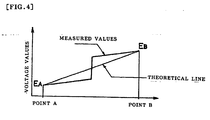
- Fig. 4 The outline of the measurement of the linearity is shown in Fig. 4 .
- the position of the pen displayed on the screen is determined from a resistance value of a portion where an upper panel and a lower panel are brought into contact with each other by pressing with the pen.
- the resistance value is determined assuming that the output voltage is distributed on the surface of the upper and lower panels according to the theoretical line (ideal line). Accordingly, if the measured voltage value deviates from the theoretical line as shown in Fig. 4 , the actual position of the pen will not well synchronize with the pen position on the screen that is determined from the resistance value. Such a deviation from the theoretical line corresponds to the linearity.
- the larger the linearity value the larger the deviation of the actual pen position from the pen position on the screen.
- sample A The transparent conductive film obtained in each Example was named sample A.
- Sample A was left in an environment at 60°C and 95%R.H. for 500 hours.
- sample B After the treatment, the sample was named sample B.
- These samples were each measured for surface electric resistance ( ⁇ /square) in the same manner as those described above, and the ratio (R B /R A ) of the resistance (R B ) of the sample B to the resistance (R A ) of the sample A was calculated for evaluation of the reliability.
Claims (12)
- Film conducteur transparent, ayant une transparence dans la gamme de la lumière visible, comprenant :- un substrat de film transparent ;- une couche de conducteur transparent, disposée sur une face du substrat de film transparent et ayant une épaisseur d de 15 nm à 35 nm, une rugosité moyenne de surface Ra de 0,37 nm à 1 nm, une rugosité maximale de surface Ry de 7,5 nm à 15 nm, Ra et Ry étant mesurées conformément à la description ; et- au moins une seule couche d'une sous-couche interposée entre le substrat de film transparent et la couche de conducteur transparent.
- Film conducteur transparent selon la revendication 1, dans lequel, dans la couche de conducteur transparent, le rapport (Ra/d) de la rugosité moyenne de surface Ra, mesurée par le procédé AFM, sur l'épaisseur d est compris entre 0,017 et 0,045.
- Film conducteur transparent selon la revendication 1, dans lequel, dans la couche de conducteur transparent, le rapport (Ry/d) de la rugosité maximale de surface Ry, mesurée comme dans la description, sur l'épaisseur d est compris entre 0,34 et 1.
- Film conducteur transparent selon l'une quelconque des revendications 1 à 3, dans lequel une première sous-couche, formée sur la face du substrat de film transparent, est faite en une matière organique.
- Film conducteur transparent selon l'une quelconque des revendications 1 à 4, dans lequel il existe au moins deux couches de sous-couches et au moins la sous-couche la plus distante de la face du substrat de film transparent est faite en une matière inorganique.
- Film conducteur transparent selon la revendication 5, dans lequel la sous-couche faite en la matière inorganique est un film de SiO2.
- Film conducteur transparent selon l'une quelconque des revendications 1 à 6, comprenant en outre un substrat transparent collé sur l'autre face du substrat de film transparent, avec une couche adhésive transparente sensible à la pression interposée entre eux.
- Film conducteur transparent selon l'une quelconque des revendications 1 à 7, dans lequel il est destiné à être utilisé dans un panneau tactile.
- Film conducteur transparent selon la revendication 8, dans lequel le panneau tactile est un panneau tactile de type à film résistif.
- Procédé de fabrication d'un film conducteur transparent selon l'une quelconque des revendications 1 à 9, comprenant les étapes consistant à :- former au moins une seule couche d'une sous-couche sur une face d'un substrat de film transparent ; et- former une couche de conducteur transparent sur la sous-couche par une pulvérisation cathodique d'une cible dans des conditions de puissance de décharge de 4 W/cm2 à 7 W/cm2, le substrat de film transparent étant chauffé à une température de 80 à 160°C.
- Procédé selon la revendication 10, comprenant en outre une étape consistant à réaliser un traitement de recuit pour obtenir une cristallisation à une température de 120°C à 160°C après l'étape de formation de la couche de conducteur transparent.
- Panneau tactile comprenant un film conducteur transparent selon l'une quelconque des revendications 1 à 9.
Applications Claiming Priority (1)
| Application Number | Priority Date | Filing Date | Title |
|---|---|---|---|
| JP2007274045A JP5099893B2 (ja) | 2007-10-22 | 2007-10-22 | 透明導電性フィルム、その製造方法及びそれを備えたタッチパネル |
Publications (3)
| Publication Number | Publication Date |
|---|---|
| EP2053079A2 EP2053079A2 (fr) | 2009-04-29 |
| EP2053079A3 EP2053079A3 (fr) | 2010-03-17 |
| EP2053079B1 true EP2053079B1 (fr) | 2013-01-09 |
Family
ID=40122352
Family Applications (1)
| Application Number | Title | Priority Date | Filing Date |
|---|---|---|---|
| EP08018392A Not-in-force EP2053079B1 (fr) | 2007-10-22 | 2008-10-21 | Film conducteur transparent, son procédé de production et panneau tactile associé |
Country Status (6)
| Country | Link |
|---|---|
| US (2) | US9428625B2 (fr) |
| EP (1) | EP2053079B1 (fr) |
| JP (1) | JP5099893B2 (fr) |
| KR (2) | KR101276431B1 (fr) |
| CN (1) | CN101417517B (fr) |
| TW (1) | TWI381400B (fr) |
Families Citing this family (49)
| Publication number | Priority date | Publication date | Assignee | Title |
|---|---|---|---|---|
| JP5788129B2 (ja) * | 2008-07-18 | 2015-09-30 | 日東電工株式会社 | 透明導電性フィルム及びタッチパネル |
| KR101050460B1 (ko) * | 2009-03-25 | 2011-07-20 | 삼성모바일디스플레이주식회사 | 유기 발광 표시 장치 및 그의 제조 방법 |
| US20120094037A1 (en) * | 2009-06-18 | 2012-04-19 | Nitto Denko Corporation | Pressure-sensitive adhesive sheet for optical use |
| JP5389568B2 (ja) * | 2009-08-19 | 2014-01-15 | 富士フイルム株式会社 | 透明導電性フィルム |
| JP2011076932A (ja) * | 2009-09-30 | 2011-04-14 | Nitto Denko Corp | 透明導電性フィルム及びタッチパネル |
| WO2011048996A1 (fr) * | 2009-10-19 | 2011-04-28 | 東洋紡績株式会社 | Film conducteur transparent |
| DE112011100972T5 (de) * | 2010-03-19 | 2013-01-17 | Sumitomo Metal Mining Co. Ltd. | Transparenter leitender Film |
| CN102243544B (zh) * | 2010-05-12 | 2013-08-14 | 群康科技(深圳)有限公司 | 触控屏、触控屏的制造方法及触控显示装置 |
| WO2012002706A2 (fr) * | 2010-06-29 | 2012-01-05 | Kolon Indurstries, Inc. | Film protecteur |
| JP2012033466A (ja) * | 2010-07-02 | 2012-02-16 | Fujifilm Corp | 導電層転写材料、及びタッチパネル |
| CN102455807A (zh) * | 2010-10-19 | 2012-05-16 | 睿明科技股份有限公司 | 触控面板的低阻抗电控线路及其制造方法 |
| JP5101719B2 (ja) | 2010-11-05 | 2012-12-19 | 日東電工株式会社 | 透明導電性フィルム、その製造方法及びそれを備えたタッチパネル |
| WO2012074059A1 (fr) * | 2010-12-02 | 2012-06-07 | 日東電工株式会社 | Film conducteur transparent et panneau tactile |
| JP6033543B2 (ja) * | 2010-12-15 | 2016-11-30 | 日東電工株式会社 | 光学用粘着シート |
| CN102534530A (zh) * | 2010-12-15 | 2012-07-04 | 电子科技大学 | 柔性pet基底ito薄膜磁控溅射制备方法 |
| JP5543907B2 (ja) * | 2010-12-24 | 2014-07-09 | 日東電工株式会社 | 透明導電性フィルムおよびその製造方法 |
| JP2012203701A (ja) * | 2011-03-25 | 2012-10-22 | Dainippon Printing Co Ltd | タッチパネル部材、透明電極層付き基板、基板積層型タッチパネル部材、および、上記タッチパネル部材または上記基板積層型タッチパネル部材を用いた座標検出装置 |
| CN102999226A (zh) * | 2011-09-12 | 2013-03-27 | 宸鸿科技(厦门)有限公司 | 反射式触控显示器及其制造方法 |
| JP2013094984A (ja) * | 2011-10-28 | 2013-05-20 | Nitto Denko Corp | 透明導電性フィルム |
| TWI544500B (zh) * | 2011-12-27 | 2016-08-01 | Sekisui Chemical Co Ltd | Transparent conductive film and electrostatic capacity type touch panel having the same, and a method for manufacturing a translucent conductive film |
| KR101392050B1 (ko) * | 2012-01-06 | 2014-05-07 | (주)엘지하우시스 | 시인성이 우수한 양면 투명 전도성 필름 및 그 제조 방법 |
| KR102087006B1 (ko) * | 2012-03-09 | 2020-03-10 | 도요보 필름 솔루션 가부시키가시야 | 투명 도전성 필름 기재용 적층체 |
| CN102736812B (zh) * | 2012-05-14 | 2016-12-14 | 浙江金徕镀膜有限公司 | 一种面板结构及其制作方法 |
| KR101539488B1 (ko) * | 2012-05-31 | 2015-07-24 | 주식회사 엘지화학 | 투명 전도성 필름 및 이를 제조하는 방법 |
| US20130319729A1 (en) * | 2012-06-01 | 2013-12-05 | Nuovo Film Inc. | Low Haze Transparent Conductive Electrodes and Method of Making the Same |
| KR101293647B1 (ko) * | 2012-07-27 | 2013-08-13 | 삼성코닝정밀소재 주식회사 | 투명 전도성 산화물 박막 기판, 그 제조방법, 이를 포함하는 유기전계발광소자 및 광전지 |
| KR101512546B1 (ko) * | 2012-10-16 | 2015-04-15 | (주)엘지하우시스 | 시인성이 개선된 투명 도전성 필름 및 이의 제조방법 |
| CN104871258B (zh) * | 2012-12-19 | 2017-05-17 | 株式会社钟化 | 带透明电极的基板及其制造方法 |
| JP6261988B2 (ja) * | 2013-01-16 | 2018-01-17 | 日東電工株式会社 | 透明導電フィルムおよびその製造方法 |
| JP6261987B2 (ja) * | 2013-01-16 | 2018-01-17 | 日東電工株式会社 | 透明導電フィルムおよびその製造方法 |
| JP6215062B2 (ja) * | 2013-01-16 | 2017-10-18 | 日東電工株式会社 | 透明導電フィルムの製造方法 |
| TW201514802A (zh) * | 2013-07-16 | 2015-04-16 | Lg Innotek Co Ltd | 觸控螢幕以及包含其之觸控裝置 |
| KR101768286B1 (ko) * | 2013-11-27 | 2017-08-16 | 주식회사 엘지화학 | 전도성 구조체 전구체, 전도성 구조체 및 이의 제조방법 |
| JP5932097B2 (ja) | 2014-04-17 | 2016-06-08 | 日東電工株式会社 | 透明導電性フィルム |
| JP6161763B2 (ja) * | 2014-04-17 | 2017-07-12 | 日東電工株式会社 | 透明導電性フィルム |
| CN106460153B (zh) * | 2014-04-30 | 2019-05-10 | 日东电工株式会社 | 透明导电性膜及其制造方法 |
| JP6211557B2 (ja) | 2014-04-30 | 2017-10-11 | 日東電工株式会社 | 透明導電性フィルム及びその製造方法 |
| CN105830170B (zh) * | 2014-05-12 | 2018-03-09 | Lg化学株式会社 | 导电结构体及其制备方法 |
| WO2016018052A1 (fr) * | 2014-07-29 | 2016-02-04 | 주식회사 엘지화학 | Stratifié conducteur et son procédé de fabrication |
| CN105320373B (zh) | 2014-07-30 | 2019-04-16 | Lg伊诺特有限公司 | 触摸板 |
| CN104485156B (zh) * | 2014-11-20 | 2017-07-28 | 张家港康得新光电材料有限公司 | 折射率匹配膜、折射率匹配膜的制作方法及触摸屏 |
| JP6577708B2 (ja) * | 2014-12-05 | 2019-09-18 | 日東電工株式会社 | 透明導電性フィルムおよびそれを用いたタッチセンサ |
| JP5905983B1 (ja) * | 2015-02-19 | 2016-04-20 | 積水化学工業株式会社 | 光透過性導電性フィルム、そのフィルムロール及びそれを有するタッチパネル |
| US20180149896A1 (en) * | 2015-05-21 | 2018-05-31 | Sharp Kabushiki Kaisha | Liquid crystal display panel |
| WO2017059444A1 (fr) * | 2015-10-01 | 2017-04-06 | The Regents Of The University Of California | Électrode transparente à nanofils d'argent thermiquement stables |
| CN105161220B (zh) * | 2015-10-09 | 2017-10-17 | 重庆文理学院 | 一种耐高温银导电薄膜的制备方法 |
| CN105869721A (zh) * | 2016-06-02 | 2016-08-17 | 南京汇金锦元光电材料有限公司 | 柔性基底界面改性的透明导电薄膜及其制备方法 |
| CN110169218B (zh) * | 2017-03-10 | 2022-05-03 | 麦克赛尔株式会社 | 电磁波吸收片 |
| CN108196732B (zh) * | 2018-01-04 | 2021-01-26 | 京东方科技集团股份有限公司 | 超声波触控装置及显示装置 |
Family Cites Families (32)
| Publication number | Priority date | Publication date | Assignee | Title |
|---|---|---|---|---|
| JPS6179647A (ja) | 1984-09-28 | 1986-04-23 | 帝人株式会社 | 透明導電性積層体及びその製造方法 |
| JPS61183809A (ja) | 1985-02-08 | 1986-08-16 | 帝人株式会社 | 透明導電性積層体及びその製造方法 |
| JP2667680B2 (ja) | 1988-08-31 | 1997-10-27 | 日東電工株式会社 | 透明導電性積層体 |
| JP2525475B2 (ja) | 1989-01-25 | 1996-08-21 | 帝人株式会社 | 透明導電性積層体 |
| JPH02276630A (ja) | 1989-01-25 | 1990-11-13 | Teijin Ltd | 透明導電性積層体およびその製造方法 |
| US5135581A (en) * | 1991-04-08 | 1992-08-04 | Minnesota Mining And Manufacturing Company | Light transmissive electrically conductive oxide electrode formed in the presence of a stabilizing gas |
| JP3086987B2 (ja) | 1992-10-21 | 2000-09-11 | キヤノン株式会社 | プローブユニットの製造方法、及びプローブユニット、及びそのプローブユニットを用いた情報処理装置 |
| JP3583163B2 (ja) | 1994-06-14 | 2004-10-27 | 出光興産株式会社 | 導電性積層体 |
| JPH0864034A (ja) * | 1994-08-26 | 1996-03-08 | Teijin Ltd | 透明導電性積層体 |
| EP0726579B1 (fr) | 1995-02-02 | 2003-11-26 | Teijin Limited | Feuille conductive transparente |
| JPH11250764A (ja) | 1998-02-27 | 1999-09-17 | Gunze Ltd | 抵抗膜型透明タッチパネル |
| JPH11286066A (ja) * | 1998-03-31 | 1999-10-19 | Oike Ind Co Ltd | 透明導電性フイルム |
| US6727566B1 (en) * | 2000-09-29 | 2004-04-27 | Matsushita Electric Industrial Co., Ltd. | Transparent substrate with conductive multilayer anti reflection film, transparent touch panel using the transparent substrate with multilayer anti reflection film and electronic apparatus using the touch panel |
| CN1353450A (zh) * | 2000-11-07 | 2002-06-12 | 赫飞科技开发股份有限公司 | 形成透明导电基板的方法 |
| JP2002163933A (ja) | 2000-11-27 | 2002-06-07 | Toyobo Co Ltd | 透明導電性フィルム、透明導電性シートおよびタッチパネル |
| WO2003012799A1 (fr) | 2001-07-31 | 2003-02-13 | Toyo Boseki Kabushiki Kaisha | Film conducteur transparent et procede de fabrication associe, feuille conductrice transparente et ecran tactile |
| US6906451B2 (en) | 2002-01-08 | 2005-06-14 | Murata Manufacturing Co., Ltd. | Piezoelectric resonator, piezoelectric filter, duplexer, communication apparatus, and method for manufacturing piezoelectric resonator |
| JP3785109B2 (ja) | 2002-04-08 | 2006-06-14 | 日東電工株式会社 | 透明導電積層体の製造方法 |
| JP2004193008A (ja) | 2002-12-12 | 2004-07-08 | Bridgestone Corp | 透明導電薄膜の成膜方法と透明導電薄膜、透明導電性フィルム及びタッチパネル |
| JP2004213990A (ja) | 2002-12-27 | 2004-07-29 | Toyobo Co Ltd | 透明導電性フィルムおよびタッチパネル |
| JP4538410B2 (ja) * | 2003-05-26 | 2010-09-08 | 日本曹達株式会社 | 透明導電膜付透光性基板の製造方法 |
| JP4324684B2 (ja) * | 2003-09-19 | 2009-09-02 | 日本ミクロコーティング株式会社 | 平坦な表面の透明導電性フィルムの製造方法 |
| JP2007042284A (ja) | 2003-10-27 | 2007-02-15 | Teijin Ltd | 透明導電性積層体及び透明タッチパネル |
| JP2007042283A (ja) | 2003-10-08 | 2007-02-15 | Teijin Ltd | 透明導電性積層体及び透明タッチパネル |
| EP1693482A4 (fr) | 2003-12-09 | 2008-04-30 | Asahi Glass Co Ltd | Film d'oxyde de titane presentant une activite photocatalytique sur l'irradiation de la lumiere visible et son procede de production |
| JP2005268616A (ja) | 2004-03-19 | 2005-09-29 | Tosoh Corp | 透明導電膜およびその製造方法 |
| WO2005109449A1 (fr) | 2004-05-07 | 2005-11-17 | Hs Planning Limited | Film conducteur pour panneau tactile et procédé de fabrication de film conducteur pour panneau tactile |
| JP3819927B2 (ja) * | 2004-06-03 | 2006-09-13 | 日東電工株式会社 | 透明導電性フィルム |
| US7972684B2 (en) | 2004-08-20 | 2011-07-05 | Teijin Limited | Transparent conductive laminated body and transparent touch-sensitive panel |
| KR100954309B1 (ko) | 2005-09-12 | 2010-04-21 | 닛토덴코 가부시키가이샤 | 투명 도전성 필름, 터치 패널용 전극판 및 터치 패널 |
| JP4943091B2 (ja) | 2005-09-12 | 2012-05-30 | 日東電工株式会社 | 透明導電性フィルム、タッチパネル用電極板およびタッチパネル |
| TW200745923A (en) | 2005-10-20 | 2007-12-16 | Nitto Denko Corp | Transparent conductive laminate body and touch panel equipped with above |
-
2007
- 2007-10-22 JP JP2007274045A patent/JP5099893B2/ja active Active
-
2008
- 2008-09-22 TW TW097136353A patent/TWI381400B/zh active
- 2008-10-14 US US12/250,645 patent/US9428625B2/en not_active Expired - Fee Related
- 2008-10-20 KR KR1020080102337A patent/KR101276431B1/ko active IP Right Grant
- 2008-10-21 EP EP08018392A patent/EP2053079B1/fr not_active Not-in-force
- 2008-10-22 CN CN2008101700744A patent/CN101417517B/zh active Active
-
2012
- 2012-06-29 US US13/538,893 patent/US20120273344A1/en not_active Abandoned
- 2012-09-24 KR KR1020120105797A patent/KR101629060B1/ko active IP Right Grant
Also Published As
| Publication number | Publication date |
|---|---|
| CN101417517B (zh) | 2012-05-30 |
| KR101276431B1 (ko) | 2013-06-19 |
| JP5099893B2 (ja) | 2012-12-19 |
| JP2009104842A (ja) | 2009-05-14 |
| KR20120127356A (ko) | 2012-11-21 |
| KR20090040850A (ko) | 2009-04-27 |
| TW200923977A (en) | 2009-06-01 |
| US9428625B2 (en) | 2016-08-30 |
| EP2053079A2 (fr) | 2009-04-29 |
| US20120273344A1 (en) | 2012-11-01 |
| EP2053079A3 (fr) | 2010-03-17 |
| CN101417517A (zh) | 2009-04-29 |
| KR101629060B1 (ko) | 2016-06-09 |
| US20090104440A1 (en) | 2009-04-23 |
| TWI381400B (zh) | 2013-01-01 |
Similar Documents
| Publication | Publication Date | Title |
|---|---|---|
| EP2053079B1 (fr) | Film conducteur transparent, son procédé de production et panneau tactile associé | |
| US8029886B2 (en) | Transparent conductive laminate and touch panel therewith | |
| EP2048672B1 (fr) | Stratifié transparent conducteur et écran tactile l'utilisant | |
| JP4314623B2 (ja) | 透明導電性積層体及びタッチパネル | |
| EP1947551B1 (fr) | Film conducteur transparent, procédé de production et panneau tactile associé | |
| JP5498537B2 (ja) | 透明導電性フィルム、その製造方法及びそれを備えたタッチパネル |
Legal Events
| Date | Code | Title | Description |
|---|---|---|---|
| PUAI | Public reference made under article 153(3) epc to a published international application that has entered the european phase |
Free format text: ORIGINAL CODE: 0009012 |
|
| AK | Designated contracting states |
Kind code of ref document: A2 Designated state(s): AT BE BG CH CY CZ DE DK EE ES FI FR GB GR HR HU IE IS IT LI LT LU LV MC MT NL NO PL PT RO SE SI SK TR |
|
| AX | Request for extension of the european patent |
Extension state: AL BA MK RS |
|
| PUAL | Search report despatched |
Free format text: ORIGINAL CODE: 0009013 |
|
| AK | Designated contracting states |
Kind code of ref document: A3 Designated state(s): AT BE BG CH CY CZ DE DK EE ES FI FR GB GR HR HU IE IS IT LI LT LU LV MC MT NL NO PL PT RO SE SI SK TR |
|
| AX | Request for extension of the european patent |
Extension state: AL BA MK RS |
|
| 17P | Request for examination filed |
Effective date: 20100915 |
|
| AKX | Designation fees paid |
Designated state(s): AT BE BG CH CY CZ DE DK EE ES FI FR GB GR HR HU IE IS IT LI LT LU LV MC MT NL NO PL PT RO SE SI SK TR |
|
| 17Q | First examination report despatched |
Effective date: 20110901 |
|
| GRAP | Despatch of communication of intention to grant a patent |
Free format text: ORIGINAL CODE: EPIDOSNIGR1 |
|
| GRAS | Grant fee paid |
Free format text: ORIGINAL CODE: EPIDOSNIGR3 |
|
| GRAA | (expected) grant |
Free format text: ORIGINAL CODE: 0009210 |
|
| AK | Designated contracting states |
Kind code of ref document: B1 Designated state(s): AT BE BG CH CY CZ DE DK EE ES FI FR GB GR HR HU IE IS IT LI LT LU LV MC MT NL NO PL PT RO SE SI SK TR |
|
| REG | Reference to a national code |
Ref country code: GB Ref legal event code: FG4D |
|
| REG | Reference to a national code |
Ref country code: AT Ref legal event code: REF Ref document number: 592735 Country of ref document: AT Kind code of ref document: T Effective date: 20130115 Ref country code: CH Ref legal event code: EP |
|
| REG | Reference to a national code |
Ref country code: IE Ref legal event code: FG4D |
|
| REG | Reference to a national code |
Ref country code: DE Ref legal event code: R096 Ref document number: 602008021469 Country of ref document: DE Effective date: 20130307 |
|
| PG25 | Lapsed in a contracting state [announced via postgrant information from national office to epo] |
Ref country code: SI Free format text: LAPSE BECAUSE OF FAILURE TO SUBMIT A TRANSLATION OF THE DESCRIPTION OR TO PAY THE FEE WITHIN THE PRESCRIBED TIME-LIMIT Effective date: 20130109 |
|
| REG | Reference to a national code |
Ref country code: NL Ref legal event code: VDEP Effective date: 20130109 |
|
| REG | Reference to a national code |
Ref country code: AT Ref legal event code: MK05 Ref document number: 592735 Country of ref document: AT Kind code of ref document: T Effective date: 20130109 |
|
| REG | Reference to a national code |
Ref country code: LT Ref legal event code: MG4D |
|
| PG25 | Lapsed in a contracting state [announced via postgrant information from national office to epo] |
Ref country code: BG Free format text: LAPSE BECAUSE OF FAILURE TO SUBMIT A TRANSLATION OF THE DESCRIPTION OR TO PAY THE FEE WITHIN THE PRESCRIBED TIME-LIMIT Effective date: 20130409 Ref country code: ES Free format text: LAPSE BECAUSE OF FAILURE TO SUBMIT A TRANSLATION OF THE DESCRIPTION OR TO PAY THE FEE WITHIN THE PRESCRIBED TIME-LIMIT Effective date: 20130420 Ref country code: BE Free format text: LAPSE BECAUSE OF FAILURE TO SUBMIT A TRANSLATION OF THE DESCRIPTION OR TO PAY THE FEE WITHIN THE PRESCRIBED TIME-LIMIT Effective date: 20130109 Ref country code: IS Free format text: LAPSE BECAUSE OF FAILURE TO SUBMIT A TRANSLATION OF THE DESCRIPTION OR TO PAY THE FEE WITHIN THE PRESCRIBED TIME-LIMIT Effective date: 20130509 Ref country code: NO Free format text: LAPSE BECAUSE OF FAILURE TO SUBMIT A TRANSLATION OF THE DESCRIPTION OR TO PAY THE FEE WITHIN THE PRESCRIBED TIME-LIMIT Effective date: 20130409 Ref country code: SE Free format text: LAPSE BECAUSE OF FAILURE TO SUBMIT A TRANSLATION OF THE DESCRIPTION OR TO PAY THE FEE WITHIN THE PRESCRIBED TIME-LIMIT Effective date: 20130109 Ref country code: AT Free format text: LAPSE BECAUSE OF FAILURE TO SUBMIT A TRANSLATION OF THE DESCRIPTION OR TO PAY THE FEE WITHIN THE PRESCRIBED TIME-LIMIT Effective date: 20130109 Ref country code: LT Free format text: LAPSE BECAUSE OF FAILURE TO SUBMIT A TRANSLATION OF THE DESCRIPTION OR TO PAY THE FEE WITHIN THE PRESCRIBED TIME-LIMIT Effective date: 20130109 |
|
| PG25 | Lapsed in a contracting state [announced via postgrant information from national office to epo] |
Ref country code: GR Free format text: LAPSE BECAUSE OF FAILURE TO SUBMIT A TRANSLATION OF THE DESCRIPTION OR TO PAY THE FEE WITHIN THE PRESCRIBED TIME-LIMIT Effective date: 20130410 Ref country code: LV Free format text: LAPSE BECAUSE OF FAILURE TO SUBMIT A TRANSLATION OF THE DESCRIPTION OR TO PAY THE FEE WITHIN THE PRESCRIBED TIME-LIMIT Effective date: 20130109 Ref country code: NL Free format text: LAPSE BECAUSE OF FAILURE TO SUBMIT A TRANSLATION OF THE DESCRIPTION OR TO PAY THE FEE WITHIN THE PRESCRIBED TIME-LIMIT Effective date: 20130109 Ref country code: PL Free format text: LAPSE BECAUSE OF FAILURE TO SUBMIT A TRANSLATION OF THE DESCRIPTION OR TO PAY THE FEE WITHIN THE PRESCRIBED TIME-LIMIT Effective date: 20130109 Ref country code: FI Free format text: LAPSE BECAUSE OF FAILURE TO SUBMIT A TRANSLATION OF THE DESCRIPTION OR TO PAY THE FEE WITHIN THE PRESCRIBED TIME-LIMIT Effective date: 20130109 Ref country code: PT Free format text: LAPSE BECAUSE OF FAILURE TO SUBMIT A TRANSLATION OF THE DESCRIPTION OR TO PAY THE FEE WITHIN THE PRESCRIBED TIME-LIMIT Effective date: 20130509 |
|
| PG25 | Lapsed in a contracting state [announced via postgrant information from national office to epo] |
Ref country code: HR Free format text: LAPSE BECAUSE OF FAILURE TO SUBMIT A TRANSLATION OF THE DESCRIPTION OR TO PAY THE FEE WITHIN THE PRESCRIBED TIME-LIMIT Effective date: 20130109 |
|
| PG25 | Lapsed in a contracting state [announced via postgrant information from national office to epo] |
Ref country code: EE Free format text: LAPSE BECAUSE OF FAILURE TO SUBMIT A TRANSLATION OF THE DESCRIPTION OR TO PAY THE FEE WITHIN THE PRESCRIBED TIME-LIMIT Effective date: 20130109 Ref country code: CZ Free format text: LAPSE BECAUSE OF FAILURE TO SUBMIT A TRANSLATION OF THE DESCRIPTION OR TO PAY THE FEE WITHIN THE PRESCRIBED TIME-LIMIT Effective date: 20130109 Ref country code: SK Free format text: LAPSE BECAUSE OF FAILURE TO SUBMIT A TRANSLATION OF THE DESCRIPTION OR TO PAY THE FEE WITHIN THE PRESCRIBED TIME-LIMIT Effective date: 20130109 Ref country code: RO Free format text: LAPSE BECAUSE OF FAILURE TO SUBMIT A TRANSLATION OF THE DESCRIPTION OR TO PAY THE FEE WITHIN THE PRESCRIBED TIME-LIMIT Effective date: 20130109 Ref country code: DK Free format text: LAPSE BECAUSE OF FAILURE TO SUBMIT A TRANSLATION OF THE DESCRIPTION OR TO PAY THE FEE WITHIN THE PRESCRIBED TIME-LIMIT Effective date: 20130109 |
|
| PLBE | No opposition filed within time limit |
Free format text: ORIGINAL CODE: 0009261 |
|
| STAA | Information on the status of an ep patent application or granted ep patent |
Free format text: STATUS: NO OPPOSITION FILED WITHIN TIME LIMIT |
|
| PG25 | Lapsed in a contracting state [announced via postgrant information from national office to epo] |
Ref country code: CY Free format text: LAPSE BECAUSE OF FAILURE TO SUBMIT A TRANSLATION OF THE DESCRIPTION OR TO PAY THE FEE WITHIN THE PRESCRIBED TIME-LIMIT Effective date: 20130109 |
|
| 26N | No opposition filed |
Effective date: 20131010 |
|
| PG25 | Lapsed in a contracting state [announced via postgrant information from national office to epo] |
Ref country code: IT Free format text: LAPSE BECAUSE OF FAILURE TO SUBMIT A TRANSLATION OF THE DESCRIPTION OR TO PAY THE FEE WITHIN THE PRESCRIBED TIME-LIMIT Effective date: 20130109 |
|
| REG | Reference to a national code |
Ref country code: DE Ref legal event code: R097 Ref document number: 602008021469 Country of ref document: DE Effective date: 20131010 |
|
| PG25 | Lapsed in a contracting state [announced via postgrant information from national office to epo] |
Ref country code: MC Free format text: LAPSE BECAUSE OF FAILURE TO SUBMIT A TRANSLATION OF THE DESCRIPTION OR TO PAY THE FEE WITHIN THE PRESCRIBED TIME-LIMIT Effective date: 20130109 |
|
| REG | Reference to a national code |
Ref country code: CH Ref legal event code: PL |
|
| REG | Reference to a national code |
Ref country code: IE Ref legal event code: MM4A |
|
| PG25 | Lapsed in a contracting state [announced via postgrant information from national office to epo] |
Ref country code: LI Free format text: LAPSE BECAUSE OF NON-PAYMENT OF DUE FEES Effective date: 20131031 Ref country code: CH Free format text: LAPSE BECAUSE OF NON-PAYMENT OF DUE FEES Effective date: 20131031 |
|
| PG25 | Lapsed in a contracting state [announced via postgrant information from national office to epo] |
Ref country code: IE Free format text: LAPSE BECAUSE OF NON-PAYMENT OF DUE FEES Effective date: 20131021 |
|
| PG25 | Lapsed in a contracting state [announced via postgrant information from national office to epo] |
Ref country code: TR Free format text: LAPSE BECAUSE OF FAILURE TO SUBMIT A TRANSLATION OF THE DESCRIPTION OR TO PAY THE FEE WITHIN THE PRESCRIBED TIME-LIMIT Effective date: 20130109 |
|
| PG25 | Lapsed in a contracting state [announced via postgrant information from national office to epo] |
Ref country code: LU Free format text: LAPSE BECAUSE OF NON-PAYMENT OF DUE FEES Effective date: 20131021 Ref country code: HU Free format text: LAPSE BECAUSE OF FAILURE TO SUBMIT A TRANSLATION OF THE DESCRIPTION OR TO PAY THE FEE WITHIN THE PRESCRIBED TIME-LIMIT; INVALID AB INITIO Effective date: 20081021 |
|
| PG25 | Lapsed in a contracting state [announced via postgrant information from national office to epo] |
Ref country code: MT Free format text: LAPSE BECAUSE OF FAILURE TO SUBMIT A TRANSLATION OF THE DESCRIPTION OR TO PAY THE FEE WITHIN THE PRESCRIBED TIME-LIMIT Effective date: 20130109 |
|
| REG | Reference to a national code |
Ref country code: FR Ref legal event code: PLFP Year of fee payment: 9 |
|
| REG | Reference to a national code |
Ref country code: FR Ref legal event code: PLFP Year of fee payment: 10 |
|
| REG | Reference to a national code |
Ref country code: FR Ref legal event code: PLFP Year of fee payment: 11 |
|
| PGFP | Annual fee paid to national office [announced via postgrant information from national office to epo] |
Ref country code: FR Payment date: 20190913 Year of fee payment: 12 |
|
| PGFP | Annual fee paid to national office [announced via postgrant information from national office to epo] |
Ref country code: DE Payment date: 20191008 Year of fee payment: 12 |
|
| PGFP | Annual fee paid to national office [announced via postgrant information from national office to epo] |
Ref country code: GB Payment date: 20191018 Year of fee payment: 12 |
|
| REG | Reference to a national code |
Ref country code: DE Ref legal event code: R119 Ref document number: 602008021469 Country of ref document: DE |
|
| GBPC | Gb: european patent ceased through non-payment of renewal fee |
Effective date: 20201021 |
|
| PG25 | Lapsed in a contracting state [announced via postgrant information from national office to epo] |
Ref country code: DE Free format text: LAPSE BECAUSE OF NON-PAYMENT OF DUE FEES Effective date: 20210501 Ref country code: FR Free format text: LAPSE BECAUSE OF NON-PAYMENT OF DUE FEES Effective date: 20201031 |
|
| PG25 | Lapsed in a contracting state [announced via postgrant information from national office to epo] |
Ref country code: GB Free format text: LAPSE BECAUSE OF NON-PAYMENT OF DUE FEES Effective date: 20201021 |