EP2048693A2 - Excimerlampe - Google Patents
Excimerlampe Download PDFInfo
- Publication number
- EP2048693A2 EP2048693A2 EP08017646A EP08017646A EP2048693A2 EP 2048693 A2 EP2048693 A2 EP 2048693A2 EP 08017646 A EP08017646 A EP 08017646A EP 08017646 A EP08017646 A EP 08017646A EP 2048693 A2 EP2048693 A2 EP 2048693A2
- Authority
- EP
- European Patent Office
- Prior art keywords
- wall panel
- reflecting film
- excimer lamp
- area
- discharge
- Prior art date
- Legal status (The legal status is an assumption and is not a legal conclusion. Google has not performed a legal analysis and makes no representation as to the accuracy of the status listed.)
- Granted
Links
Images


Classifications
-
- H—ELECTRICITY
- H01—ELECTRIC ELEMENTS
- H01J—ELECTRIC DISCHARGE TUBES OR DISCHARGE LAMPS
- H01J65/00—Lamps without any electrode inside the vessel; Lamps with at least one main electrode outside the vessel
-
- H—ELECTRICITY
- H01—ELECTRIC ELEMENTS
- H01J—ELECTRIC DISCHARGE TUBES OR DISCHARGE LAMPS
- H01J61/00—Gas-discharge or vapour-discharge lamps
- H01J61/02—Details
- H01J61/30—Vessels; Containers
- H01J61/35—Vessels; Containers provided with coatings on the walls thereof; Selection of materials for the coatings
-
- H—ELECTRICITY
- H01—ELECTRIC ELEMENTS
- H01J—ELECTRIC DISCHARGE TUBES OR DISCHARGE LAMPS
- H01J65/00—Lamps without any electrode inside the vessel; Lamps with at least one main electrode outside the vessel
- H01J65/04—Lamps in which a gas filling is excited to luminesce by an external electromagnetic field or by external corpuscular radiation, e.g. for indicating plasma display panels
-
- H—ELECTRICITY
- H01—ELECTRIC ELEMENTS
- H01J—ELECTRIC DISCHARGE TUBES OR DISCHARGE LAMPS
- H01J65/00—Lamps without any electrode inside the vessel; Lamps with at least one main electrode outside the vessel
- H01J65/04—Lamps in which a gas filling is excited to luminesce by an external electromagnetic field or by external corpuscular radiation, e.g. for indicating plasma display panels
- H01J65/042—Lamps in which a gas filling is excited to luminesce by an external electromagnetic field or by external corpuscular radiation, e.g. for indicating plasma display panels by an external electromagnetic field
- H01J65/046—Lamps in which a gas filling is excited to luminesce by an external electromagnetic field or by external corpuscular radiation, e.g. for indicating plasma display panels by an external electromagnetic field the field being produced by using capacitive means around the vessel
-
- H—ELECTRICITY
- H05—ELECTRIC TECHNIQUES NOT OTHERWISE PROVIDED FOR
- H05B—ELECTRIC HEATING; ELECTRIC LIGHT SOURCES NOT OTHERWISE PROVIDED FOR; CIRCUIT ARRANGEMENTS FOR ELECTRIC LIGHT SOURCES, IN GENERAL
- H05B41/00—Circuit arrangements or apparatus for igniting or operating discharge lamps
- H05B41/14—Circuit arrangements
- H05B41/26—Circuit arrangements in which the lamp is fed by power derived from DC by means of a converter, e.g. by high-voltage DC
- H05B41/28—Circuit arrangements in which the lamp is fed by power derived from DC by means of a converter, e.g. by high-voltage DC using static converters
- H05B41/2806—Circuit arrangements in which the lamp is fed by power derived from DC by means of a converter, e.g. by high-voltage DC using static converters with semiconductor devices and specially adapted for lamps without electrodes in the vessel, e.g. surface discharge lamps, electrodeless discharge lamps
Definitions
- This invention relates to excimer lamps that emit UV radiation; more precisely, it relates to excimer lamps in which a UV-reflecting film is formed on the inner surfaces of a discharge vessel facing the discharge space.
- excimer lamps have been employed as UV light sources for surface finishing when performing such processes as cleaning, ashing or coating by irradiation with UV radiation in, for example, the manufacturing of semiconductor devices, liquid crystal displays, etc.
- UV radiation hit this kind of body UV-reflecting film composed of laminated UV scattering particles it is scattered in a direction which is different from the initial direction of the UV radiation by being refracted or reflected on the surfaces of numerous UV scattering particles.
- silica glass is widely employed as the material for discharge vessels in lamps that emit UV radiation, such as an excimer lamp.
- some types of excimer lamps are constructed in such a way that both ends are hermetically sealed and are provided with a nearly cylindrically shaped silica glass discharge vessel 20 inside of which is a discharge space S, and the outside of which are a top wall panel 21, bottom wall panel 23, side wall panels 25 and end wall panels 26 which enclose the discharge space S which contains the discharge gas.
- a discharge space S is a discharge space S
- a top wall panel 21, bottom wall panel 23 side wall panels 25 and end wall panels 26 which enclose the discharge space S which contains the discharge gas.
- an electrode 11 and another electrode 12 are installed opposite from each other.
- the UV-reflecting film 50 is formed on the inner surface 21 B of top wall panel 21 on which one of the electrodes 11 is formed and also, a light exit window for emitting UV radiation generated in the discharge space S through an area where there no UV reflective coating 50 is formed on the inner surface of the discharge vessel 20 (specifically, the inner surface 23B of the bottom wall panel 23 and the inner surface 25A of the side wall panel 25.
- 28 is a chip tube and 29 is a flange.
- the discharge vessel 20 and the UV-reflecting film 50 function as a dielectric body and, in discharge space S, a discharge starting point is generated on the surface facing discharge space S on the UV-reflecting film 50 and the bottom wall panel 23 facing the UV-reflecting film 50 (specifically, the surface 51 of the UV-reflecting film and the inner surface 23B of the bottom wall panel 23), and as a result, dielectric barrier discharge occurs and through this dielectric barrier discharge, excimer molecules are formed in the discharge gas and UV radiation is emitted from the light exit window comprised of the bottom wall panel 23 and the side wall panels 25 of the discharge vessel 20.
- a primary object of this invention is to devise an excimer lamp that can produce UV irradiation with high efficiency, and moreover, can irradiate the target surface of a target body with a high rate of uniformity in addition to having a UV-reflective layer that does not peel.
- an excimer lamp in accordance with the present invention by the lamp being comprised of a top wall panel and a bottom wall panel facing said top wall panel, and a pair of side wall panels connecting said top wall panel and bottom wall panel and a pair of end wall panels connecting these top, bottom and pair of side wall panels respectively and, in the internal space enclosed by the top, bottom, side and end wall panels, a silica glass discharge vessel containing the discharge gas which forms the excimer molecules by dielectric barrier discharge, and in the excimer lamp which has an electrode formed on the outer surface of the top wall panel and another electrode formed on the outer surface of the bottom wall panel installed opposite each other on said discharge vessel and, on the inner surface of the above-mentioned discharge vessel, a UV-reflecting film comprised of silica particles and alumina particles is at least formed on the inner surface area of the side wall panel, with a percentage of silica particles of 30 weight % or more.
- the UV-reflecting film is on the inner surface area of the end wall panels as well.
- this UV-reflecting film has a specified composition, and in addition, prevents the occurrence of abnormal discharge by being formed, at least, on the inner surface area of the side wall panels on the inner surface of the discharge vessel, and since, inside the discharge vessel, a countless number of columnar arc discharges having nearly uniformly identical discharge power can be generated, it can prevent the occurrence of abnormal discharge resulting in unevenness in illuminance on the target surface of the target body and the occurrence of peeling of the end area of the UV-reflecting film, so that UV radiation can be irradiated with a high degree of efficiency and furthermore
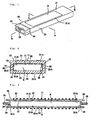
- Fig. 1 is a perspective drawing showing an example of the structure of the excimer lamp of the invention.
- Fig. 2 is a sectional view taken along line A-A of the excimer lamp shown in Fig. 1 .
- Fig. 3 is a sectional view taken along line B-B of the excimer lamp shown in Fig. 1 .
- Fig. 6 is a sectional view showing yet another example of the structure of the excimer lamp the present invention.
- Fig. 7 is a sectional view showing yet another example of the structure of the excimer lamp the present invention.
- Fig. 8 is a sectional view showing yet another example of the structure of the excimer lamp the present invention.
- Fig. 10 is a sectional view showing an example of the structure of an existing excimer lamp.
- Fig. 11 is a sectional view taken along A-A of the excimer lamp in Fig. 10 .
- Fig. 1 is a perspective drawing that shows an example of the configuration of the excimer lamp of the invention
- Fig. 2 is a drawing that shows the A-A cross-sectional area of the excimer lamp in Fig. 1
- Fig. 3 is a drawing that shows the B-B cross-sectional area of the excimer lamp in Fig. 1 .
- both ends of this excimer lamp are hermetically sealed and it is provided with a nearly cylindrical-shaped silica glass discharge vessel 20 whose inside forms the discharge space S.
- This discharge vessel 20 is bounded by a top wall panel 21, a bottom wall panel 23 facing the top wall panel 21, a pair of side wall panels 25 connecting the top wall panel 21 and the bottom wall panel 23, and a pair of end wall panels 26 installed so as to hermetically seal both ends of a square cylinder-shaped body.
- the top wall 21, bottom wall 23 and pair of side wall panels 25 enclose a nearly square column-shaped internal a discharge space S, in which is disposed a discharge gas, such as, for example, xenon, in which excimer molecules are formed by dielectric barrier discharge.
- Electrodes 11, 12 are formed by vacuum evaporation of such metals as, for example, gold (Au) and also, are connected to an appropriate high frequency power supply (not shown).
- a UV-reflecting film 30 of, for example, 10-1000 ⁇ m thickness, is formed at least on the inner surface area of the side wall panels, and furthermore, a light exit window for emitting UV radiation generated in discharge space S is formed in an area on the inner surface of the discharge vessel 20 where there is no UV-reflecting film 30.
- the inner surface area of the side wall panels means the inner surface 25A of the side wall panels 25 facing the discharge space S. Also, in order to connect the edge 22 of the flat top wall panel 21 to the edge 24 of the flat bottom wall panel 23, the side wall panels 25 are installed in the area between them and constitute wall panels of the discharge vessel 20.
- the UV-reflecting film 30 is formed on the inner surface 21B of the top wall panel 21 and the upper wall panel side areas of the inner surfaces 25A (upper area in Fig. 2 of the side wall panels 25 of discharge vessel 20; in other words, so as to stretch across the area from the upper wall panel area of one (right side in Fig. 2 ) side wall panel side area 25, to the upper wall panel side area of the other (left side in Fig. 2 ) side wall panel 25, including the inner surface 21B of the top wall panel 21.
- a light exit window is formed by an area on the inner surface of the discharge vessel 20, specifically, the bottom wall panel area (lower area in Fig. 2 of the bottom wall panel 23) and the side wall panels 25, where no UV-reflecting film is formed.
- the UV-reflecting film 30 is comprised of silicon oxide (silica) and aluminum oxide (alumina) particles and these silica and alumina particles (hereafter referred to collectively as "specified UV scattering particles") are laminated.
- Emitted UV radiation is refracted and reflected on the surfaces of numerous specified UV scattering particles by the UV-reflecting film 30, and consequently, they are scattered in directions different from the direction from which they were radiated.
- the proportion of silica particles contained in the UV-reflecting film 30 is at least 30 weight % and preferably 30-99 weight %, and more preferably, 40-99 weight %.
- the proportion of the alumina particles that are contained is preferably 1-70 weight %, even more preferably 5-70 weight % and most preferably 10-70 weight %.
- the silica particles of which the UV-reflecting film 30 is comprised may either be in a glassy state or a crystalline state, but particles in a glassy state are preferable.
- the particle diameter of silica particles is 2 to 8 ⁇ m and furthermore, it is desirable for the mean particle diameter to be 4 ⁇ m.
- silica particles as well as having a high degree of UV reflectivity, are made from the same material as the discharge vessel 20 and have a high degree of adhesion to both the discharge vessel 20 and the alumina particles. Therefore, the UV-reflecting film 30, which is made from these silica particles, has a high degree of adhesion to the discharge vessel 20.
- the alumina particles used in the UV-reflecting film 30 are normally crystallized, since they have the characteristic of being easy to crystallize and difficult to change to a glassy state.
- the particle diameter of the alumina particles is about 2 to 6 ⁇ m and also, it is desirable for the mean particle diameter to be 4 ⁇ m.
- the index of refraction of alumina particles is greater, and since, therefore, they have the characteristic of having a high degree of reflectivity, the UV-reflecting film which; together with silica particles, is composed of alumina particles having this kind of special quality has an excellent UV-reflecting capability.
- the part equivalent to a globular part in the starting material including when the silica particles melt and form clumps, is considered to be a particle.
- the Feret diameter is considered to be the distance between two perpendicular lines into which a particle fits.
- mean particle diameter means using, for example, a Hitachi field emission scanning electron microscope (S4100) and measuring the particle diameter of over one hundred particles under the conditions of 10 to20 kV acceleration voltage (when magnification is 20,000 times for particles with a diameter of 0.3 ⁇ m, for example) and calculating the distribution (counting) of the value of the measurement of the particle diameters and the mean range where the incidence is at its greatest.
- This mean value regarded to be the mean particle diameter, is obtained, for example, by dividing the range between the maximum value and the minimum value of the measured particle diameters into 15 zones and considering the number of particle diameters belonging to each of the zones to be the number of said zone; the mean value is the value of the zone with the largest number among these 15 zones.
- This kind of UV-reflecting film 30 can be formed by the following steps, for example, in the flow-down method, specifically, by combining silica particles and alumina particles with a suitable solvent and obtaining a reflecting film forming liquid; then by pouring this reflecting film forming liquid into the area where the UV-reflecting film 30 is to be formed on the inner surface of the discharge vessel tube for forming the discharge vessel 20, a thin layer is formed and by drying and calcinating this thin layer, it can be formed.
- the thickness of the resulting UV-reflecting film 30 can be adjusted; specifically, in order to make it thinner, the viscosity of the liquid is lowered, and also, in order to make it thicker, the viscosity of the liquid is increased.
- An excimer lamp constructed as above has a discharge vessel 20 and a UV-reflecting film 30 that functions as a dielectric by having an appropriately sized, controlled high frequency voltage from a high frequency power source applied between electrode 11 and electrode 12, and in discharge space S, discharge starting points occur on the surfaces (specifically, the surface 31 of UV-reflecting film 30 and the inner surface 23B of bottom wall panel 23 facing the UV-reflecting film 30 and the discharge space S of the bottom wall panel 23 opposite this UV-reflecting film 30 and, as a result of this, dielectric barrier discharge occurs and by this dielectric barrier discharge, excimer molecules in the discharge gas are formed and UV radiation is emitted from the light exit window comprised of the bottom wall panel 23 and the bottom wall panel side areas of the side wall panels 25 of the discharge vessel 20.
- UV radiation generated in the discharge space S and emitted in the direction of the UV-reflecting film 30 and in directions other than the direction of the light exit window can be emitted from the light exit window by being reflected by said UV-reflecting film 30, together with the UV radiation radiated directly in the direction of the light exit window.
- this UV-reflecting film 30 contains a specified proportion of silica particles and alumina particles and, moreover, extends not only to the inner surface area of the top wall panel (the inner surface 21B of top wall panel 21) on the inner surface of the discharge vessel 20, but as far as the inner surface area of the side wall panel (the inner surface 25A of side wall panel 25) that connects the inner surface area of the top wall panel and this end area 35, and by being located on said inner surface area of the side wall panel, prevents the occurrence of abnormal discharge and, in discharge space S, almost uniformly generates a large number of columnar arc discharges with the same discharge power. As a result, the generation of abnormal discharges causing the unevenness in illuminance on the target surface of the target body that and peeling of the end area 35 of the UV-reflecting film 30 can be prevented.
- UV radiation can be emitted with a high degree of efficiency, and furthermore, since the generation of abnormal discharges is prevented, the target surface of the target body can be irradiated with a high degree of uniformity, and peeling of the end area 35 of said UV-reflecting film 30 can be prevented.
- the UV-reflecting film 30 extends not only to the inner surface 21B of the top wall panel 21, but also to the inner surfaces 25A (inner surface area of the side wall panel) of the side wall panels 25 and since the ends 35 are not located directly underneath the electrode 11, the accumulation of electrical charge in said ends 35 is neutralized, resulting in a state in which it is considered to be difficult for abnormal discharges per se to occur. Furthermore, the surface of the UV-reflecting film 30 has an unevenness that arises from its constituent particles, and it may be that, since the creeping distance is also lengthened, a state occurs in which abnormal discharges per se arc difficult.
- the side wall panels 45 are installed in the area between them and constitute wall panels of the discharge vessel 40.
- the example of an excimer lamp in Fig. 5 is provided with a discharge vessel 40 that has a side wall panel 45 consisting of a curved panel and other than being formed in the area mentioned below, the UV-reflecting film 30 has a structure identical to that of the excimer lamp in Fig. 4 .
- the UV-reflecting film 30 is formed in each of the two areas; from the electrode edge opposing location d opposite the location of the edge of the electrode 11 on the cuter surface 41A of the top wall panel 41, to the electrode edge opposing location e opposite the location of the edge of the other electrode 12 on the outer surface 43A of the bottom wall panel 43 on the inner surface of the discharge vessel 40
- a UV-reflecting film 30 is formed to stretch across the area from the point of intersection N1 (right side of Fig. 3 ) with a straight line N on the inner surface 41B of the top wall panel 41, to the point of intersection N2 with the straight line N on the inner surface 43B of the bottom wall panel 43, including the inner surface 45A of the side wall panels 45.
- the other UV-reflecting film 30 is formed so as to stretch across the area from the point of intersection (N1) (left side of Fig. 8 ) with the other straight line N on the inner surface 41B of top wall panel 41, to the point of intersectional N2 with the other straight line N on the inner surface 43B of the bottom wall panel 43, including the inner surface 45A of side wall panel 45.
- separate light exit windows are formed by each of the two areas of the top wall panel 41 and the bottom wall panel 43 where UV-reflecting film 30 is not formed.
Landscapes
- Physics & Mathematics (AREA)
- Engineering & Computer Science (AREA)
- Plasma & Fusion (AREA)
- Electromagnetism (AREA)
- Vessels And Coating Films For Discharge Lamps (AREA)
Applications Claiming Priority (1)
| Application Number | Priority Date | Filing Date | Title |
|---|---|---|---|
| JP2007265350A JP4946773B2 (ja) | 2007-10-11 | 2007-10-11 | エキシマランプ |
Publications (3)
| Publication Number | Publication Date |
|---|---|
| EP2048693A2 true EP2048693A2 (de) | 2009-04-15 |
| EP2048693A3 EP2048693A3 (de) | 2009-07-01 |
| EP2048693B1 EP2048693B1 (de) | 2016-08-24 |
Family
ID=40317044
Family Applications (1)
| Application Number | Title | Priority Date | Filing Date |
|---|---|---|---|
| EP08017646.4A Active EP2048693B1 (de) | 2007-10-11 | 2008-10-08 | Excimerlampe |
Country Status (6)
| Country | Link |
|---|---|
| US (1) | US7714511B2 (de) |
| EP (1) | EP2048693B1 (de) |
| JP (1) | JP4946773B2 (de) |
| KR (1) | KR101175387B1 (de) |
| CN (1) | CN101409204B (de) |
| TW (1) | TWI416583B (de) |
Families Citing this family (15)
| Publication number | Priority date | Publication date | Assignee | Title |
|---|---|---|---|---|
| JP4748208B2 (ja) * | 2008-11-18 | 2011-08-17 | ウシオ電機株式会社 | エキシマ放電ランプおよびエキシマ放電ランプの製造方法 |
| DE102010015495B4 (de) * | 2010-04-16 | 2012-04-26 | Fraunhofer-Gesellschaft zur Förderung der angewandten Forschung e.V. | Vorrichtung zum Erzeugen von UV-Licht |
| JP5376410B2 (ja) * | 2011-03-11 | 2013-12-25 | ウシオ電機株式会社 | エキシマランプ |
| WO2013114718A1 (ja) * | 2012-02-02 | 2013-08-08 | ウシオ電機株式会社 | エキシマランプおよびエキシマランプの発光管の製造方法 |
| JP6016059B2 (ja) * | 2012-03-30 | 2016-10-26 | ウシオ電機株式会社 | エキシマランプ |
| JP5773277B2 (ja) * | 2012-04-27 | 2015-09-02 | 株式会社Gsユアサ | 誘電体バリア放電ランプ |
| JP5773276B2 (ja) * | 2012-04-27 | 2015-09-02 | 株式会社Gsユアサ | 誘電体バリア放電ランプ |
| CN103377873B (zh) * | 2012-04-27 | 2017-04-12 | 株式会社杰士汤浅国际 | 电介质阻挡放电灯 |
| US9153427B2 (en) | 2012-12-18 | 2015-10-06 | Agilent Technologies, Inc. | Vacuum ultraviolet photon source, ionization apparatus, and related methods |
| JP2015032378A (ja) * | 2013-07-31 | 2015-02-16 | 株式会社Gsユアサ | 放電ランプ |
| JP6233017B2 (ja) * | 2013-12-27 | 2017-11-22 | 株式会社ニコン | フッ化カルシウム光学部材、フッ化カルシウム部材の製造方法、及びフッ化カルシウム単結晶の加工方法 |
| JP7384090B2 (ja) * | 2020-03-26 | 2023-11-21 | ウシオ電機株式会社 | エキシマランプ、光照射装置 |
| US11786622B2 (en) | 2020-05-08 | 2023-10-17 | Ultra-Violet Solutions, Llc | Far UV-C light apparatus |
| JP7842977B2 (ja) * | 2021-06-21 | 2026-04-09 | ウシオ電機株式会社 | エキシマランプ装置 |
| CN121171878B (zh) * | 2025-11-24 | 2026-02-06 | 苏州汇影光学技术有限公司 | 一种多电极六面体准分子灯及其制造工艺 |
Citations (1)
| Publication number | Priority date | Publication date | Assignee | Title |
|---|---|---|---|---|
| JP3580233B2 (ja) | 2000-09-19 | 2004-10-20 | ウシオ電機株式会社 | 誘電体バリア放電ランプ装置 |
Family Cites Families (14)
| Publication number | Priority date | Publication date | Assignee | Title |
|---|---|---|---|---|
| JPH0636348B2 (ja) * | 1989-02-23 | 1994-05-11 | 日亜化学工業株式会社 | 高演色型蛍光ランプ |
| JPH02257562A (ja) * | 1989-03-30 | 1990-10-18 | Toshiba Lighting & Technol Corp | 蛍光ランプ |
| JPH06338300A (ja) * | 1993-05-27 | 1994-12-06 | Ushio Inc | 誘電体バリヤ放電ランプとそれを使用した処理方法 |
| JP3491566B2 (ja) * | 1999-07-05 | 2004-01-26 | ウシオ電機株式会社 | 誘電体バリア放電ランプ |
| JP2000200690A (ja) | 2000-01-01 | 2000-07-18 | Ushio Inc | 誘電体バリア放電ランプ光源装置 |
| DE10051124A1 (de) * | 2000-10-14 | 2002-04-25 | Philips Corp Intellectual Pty | UV-reflektierende Schicht, Lampe mit einer solchen Schicht und Verfahren zum Aufbringen einer solchen Schicht auf ein Lampenglas |
| JP4500162B2 (ja) * | 2002-05-29 | 2010-07-14 | コーニンクレッカ フィリップス エレクトロニクス エヌ ヴィ | 紫外線反射層を具える蛍光ランプ |
| JP4221561B2 (ja) * | 2002-10-02 | 2009-02-12 | 株式会社ジーエス・ユアサコーポレーション | エキシマランプ |
| DE10345771A1 (de) * | 2003-10-01 | 2005-04-21 | Patent Treuhand Ges Fuer Elektrische Gluehlampen Mbh | Reflexionsschichten aus Aluminiumoxidpartikel-Mischung |
| KR20050093946A (ko) * | 2004-03-17 | 2005-09-26 | 삼성전자주식회사 | 면광원 장치 및 이를 갖는 액정표시장치 |
| JP2005347025A (ja) * | 2004-06-01 | 2005-12-15 | Japan Storage Battery Co Ltd | 誘電体バリア放電ランプ |
| KR20060003164A (ko) * | 2004-07-05 | 2006-01-10 | 삼성전자주식회사 | 평판형 형광램프 |
| KR20060016218A (ko) | 2004-08-17 | 2006-02-22 | 삼성코닝 주식회사 | 광촉매층을 구비하는 평판 램프 |
| JP4749797B2 (ja) * | 2005-08-10 | 2011-08-17 | 株式会社オーク製作所 | エキシマランプ |
-
2007
- 2007-10-11 JP JP2007265350A patent/JP4946773B2/ja active Active
-
2008
- 2008-08-04 TW TW097129518A patent/TWI416583B/zh active
- 2008-08-26 KR KR1020080083267A patent/KR101175387B1/ko active Active
- 2008-10-08 EP EP08017646.4A patent/EP2048693B1/de active Active
- 2008-10-09 US US12/248,396 patent/US7714511B2/en active Active
- 2008-10-13 CN CN2008101701501A patent/CN101409204B/zh active Active
Patent Citations (1)
| Publication number | Priority date | Publication date | Assignee | Title |
|---|---|---|---|---|
| JP3580233B2 (ja) | 2000-09-19 | 2004-10-20 | ウシオ電機株式会社 | 誘電体バリア放電ランプ装置 |
Also Published As
| Publication number | Publication date |
|---|---|
| US20090096377A1 (en) | 2009-04-16 |
| US7714511B2 (en) | 2010-05-11 |
| TWI416583B (zh) | 2013-11-21 |
| EP2048693A3 (de) | 2009-07-01 |
| CN101409204B (zh) | 2012-02-29 |
| KR101175387B1 (ko) | 2012-08-20 |
| JP4946773B2 (ja) | 2012-06-06 |
| JP2009093986A (ja) | 2009-04-30 |
| CN101409204A (zh) | 2009-04-15 |
| EP2048693B1 (de) | 2016-08-24 |
| KR20090037295A (ko) | 2009-04-15 |
| TW200917321A (en) | 2009-04-16 |
Similar Documents
| Publication | Publication Date | Title |
|---|---|---|
| EP2048693B1 (de) | Excimerlampe | |
| CN101896992B (zh) | 放电灯 | |
| EP2056336B1 (de) | Excimerlampen | |
| JP2010027268A (ja) | エキシマランプ | |
| CN101599414B (zh) | 准分子灯 | |
| KR20010022965A (ko) | 유전적으로 차단된 전극을 가진 방전램프 | |
| CN101031993B (zh) | 紫外线灯及紫外线照射装置 | |
| JP3889987B2 (ja) | 放電灯装置及びバックライト | |
| JP5092700B2 (ja) | エキシマランプ | |
| JP2006302720A (ja) | エキシマランプ | |
| CN101599413A (zh) | 准分子灯 | |
| JP5303905B2 (ja) | エキシマランプ | |
| KR20070034947A (ko) | 백라이트 시스템 | |
| US20050116639A1 (en) | Plasma flat lamp | |
| JP3025390B2 (ja) | 誘電体バリヤ放電ランプ | |
| JP3439749B2 (ja) | 発光デバイス | |
| US6906461B2 (en) | Light source device with inner and outer electrodes and liquid crystal display device | |
| TWI470668B (zh) | Discharge lamp | |
| KR100307445B1 (ko) | 면광원장치 | |
| JP2001126669A (ja) | 平面形希ガス蛍光ランプ | |
| JP2001126667A (ja) | 平面形希ガス蛍光ランプ | |
| JP2008243521A (ja) | 誘電体バリア型放電ランプ | |
| JP2005011772A (ja) | 平面型放電管 | |
| JP2004234955A (ja) | 二次元アレー型誘電体バリア放電装置 | |
| JP2004152710A (ja) | 平板型エキシマランプ |
Legal Events
| Date | Code | Title | Description |
|---|---|---|---|
| PUAI | Public reference made under article 153(3) epc to a published international application that has entered the european phase |
Free format text: ORIGINAL CODE: 0009012 |
|
| AK | Designated contracting states |
Kind code of ref document: A2 Designated state(s): AT BE BG CH CY CZ DE DK EE ES FI FR GB GR HR HU IE IS IT LI LT LU LV MC MT NL NO PL PT RO SE SI SK TR |
|
| AX | Request for extension of the european patent |
Extension state: AL BA MK RS |
|
| PUAL | Search report despatched |
Free format text: ORIGINAL CODE: 0009013 |
|
| RIC1 | Information provided on ipc code assigned before grant |
Ipc: H01J 65/04 20060101ALI20090520BHEP Ipc: H01J 65/00 20060101AFI20090210BHEP |
|
| AK | Designated contracting states |
Kind code of ref document: A3 Designated state(s): AT BE BG CH CY CZ DE DK EE ES FI FR GB GR HR HU IE IS IT LI LT LU LV MC MT NL NO PL PT RO SE SI SK TR |
|
| AX | Request for extension of the european patent |
Extension state: AL BA MK RS |
|
| 17P | Request for examination filed |
Effective date: 20090724 |
|
| AKX | Designation fees paid |
Designated state(s): AT DE GB NL |
|
| 17Q | First examination report despatched |
Effective date: 20100507 |
|
| GRAP | Despatch of communication of intention to grant a patent |
Free format text: ORIGINAL CODE: EPIDOSNIGR1 |
|
| INTG | Intention to grant announced |
Effective date: 20160426 |
|
| GRAS | Grant fee paid |
Free format text: ORIGINAL CODE: EPIDOSNIGR3 |
|
| GRAA | (expected) grant |
Free format text: ORIGINAL CODE: 0009210 |
|
| RAP1 | Party data changed (applicant data changed or rights of an application transferred) |
Owner name: USHIO DENKI KABUSHIKI KAISHA |
|
| RAP1 | Party data changed (applicant data changed or rights of an application transferred) |
Owner name: USHIO DENKI KABUSHIKI KAISHA |
|
| AK | Designated contracting states |
Kind code of ref document: B1 Designated state(s): AT DE GB NL |
|
| REG | Reference to a national code |
Ref country code: GB Ref legal event code: FG4D |
|
| REG | Reference to a national code |
Ref country code: NL Ref legal event code: FP |
|
| REG | Reference to a national code |
Ref country code: AT Ref legal event code: REF Ref document number: 823744 Country of ref document: AT Kind code of ref document: T Effective date: 20160915 |
|
| REG | Reference to a national code |
Ref country code: DE Ref legal event code: R096 Ref document number: 602008045829 Country of ref document: DE |
|
| REG | Reference to a national code |
Ref country code: DE Ref legal event code: R097 Ref document number: 602008045829 Country of ref document: DE |
|
| PLBE | No opposition filed within time limit |
Free format text: ORIGINAL CODE: 0009261 |
|
| STAA | Information on the status of an ep patent application or granted ep patent |
Free format text: STATUS: NO OPPOSITION FILED WITHIN TIME LIMIT |
|
| 26N | No opposition filed |
Effective date: 20170526 |
|
| REG | Reference to a national code |
Ref country code: AT Ref legal event code: UEP Ref document number: 823744 Country of ref document: AT Kind code of ref document: T Effective date: 20160824 |
|
| REG | Reference to a national code |
Ref country code: DE Ref legal event code: R082 Ref document number: 602008045829 Country of ref document: DE Representative=s name: MAIWALD GMBH, DE |
|
| PGFP | Annual fee paid to national office [announced via postgrant information from national office to epo] |
Ref country code: NL Payment date: 20250912 Year of fee payment: 18 |
|
| PGFP | Annual fee paid to national office [announced via postgrant information from national office to epo] |
Ref country code: GB Payment date: 20250828 Year of fee payment: 18 |
|
| PGFP | Annual fee paid to national office [announced via postgrant information from national office to epo] |
Ref country code: DE Payment date: 20250902 Year of fee payment: 18 |
|
| PGFP | Annual fee paid to national office [announced via postgrant information from national office to epo] |
Ref country code: AT Payment date: 20250925 Year of fee payment: 18 |