EP2041958B1 - Ccd with improved substrate voltage setting circuit - Google Patents
Ccd with improved substrate voltage setting circuit Download PDFInfo
- Publication number
- EP2041958B1 EP2041958B1 EP07810576.4A EP07810576A EP2041958B1 EP 2041958 B1 EP2041958 B1 EP 2041958B1 EP 07810576 A EP07810576 A EP 07810576A EP 2041958 B1 EP2041958 B1 EP 2041958B1
- Authority
- EP
- European Patent Office
- Prior art keywords
- image sensor
- pixels
- substrate voltage
- charge
- voltage
- Prior art date
- Legal status (The legal status is an assumption and is not a legal conclusion. Google has not performed a legal analysis and makes no representation as to the accuracy of the status listed.)
- Active
Links
Images


Classifications
-
- H—ELECTRICITY
- H04—ELECTRIC COMMUNICATION TECHNIQUE
- H04N—PICTORIAL COMMUNICATION, e.g. TELEVISION
- H04N25/00—Circuitry of solid-state image sensors [SSIS]; Control thereof
-
- H—ELECTRICITY
- H04—ELECTRIC COMMUNICATION TECHNIQUE
- H04N—PICTORIAL COMMUNICATION, e.g. TELEVISION
- H04N25/00—Circuitry of solid-state image sensors [SSIS]; Control thereof
- H04N25/40—Extracting pixel data from image sensors by controlling scanning circuits, e.g. by modifying the number of pixels sampled or to be sampled
- H04N25/42—Extracting pixel data from image sensors by controlling scanning circuits, e.g. by modifying the number of pixels sampled or to be sampled by switching between different modes of operation using different resolutions or aspect ratios, e.g. switching between interlaced and non-interlaced mode
-
- H—ELECTRICITY
- H04—ELECTRIC COMMUNICATION TECHNIQUE
- H04N—PICTORIAL COMMUNICATION, e.g. TELEVISION
- H04N25/00—Circuitry of solid-state image sensors [SSIS]; Control thereof
- H04N25/40—Extracting pixel data from image sensors by controlling scanning circuits, e.g. by modifying the number of pixels sampled or to be sampled
- H04N25/46—Extracting pixel data from image sensors by controlling scanning circuits, e.g. by modifying the number of pixels sampled or to be sampled by combining or binning pixels
-
- H—ELECTRICITY
- H04—ELECTRIC COMMUNICATION TECHNIQUE
- H04N—PICTORIAL COMMUNICATION, e.g. TELEVISION
- H04N25/00—Circuitry of solid-state image sensors [SSIS]; Control thereof
- H04N25/60—Noise processing, e.g. detecting, correcting, reducing or removing noise
- H04N25/62—Detection or reduction of noise due to excess charges produced by the exposure, e.g. smear, blooming, ghost image, crosstalk or leakage between pixels
- H04N25/621—Detection or reduction of noise due to excess charges produced by the exposure, e.g. smear, blooming, ghost image, crosstalk or leakage between pixels for the control of blooming
- H04N25/622—Detection or reduction of noise due to excess charges produced by the exposure, e.g. smear, blooming, ghost image, crosstalk or leakage between pixels for the control of blooming by controlling anti-blooming drains
-
- H—ELECTRICITY
- H04—ELECTRIC COMMUNICATION TECHNIQUE
- H04N—PICTORIAL COMMUNICATION, e.g. TELEVISION
- H04N25/00—Circuitry of solid-state image sensors [SSIS]; Control thereof
- H04N25/70—SSIS architectures; Circuits associated therewith
- H04N25/71—Charge-coupled device [CCD] sensors; Charge-transfer registers specially adapted for CCD sensors
- H04N25/73—Charge-coupled device [CCD] sensors; Charge-transfer registers specially adapted for CCD sensors using interline transfer [IT]
-
- H—ELECTRICITY
- H10—SEMICONDUCTOR DEVICES; ELECTRIC SOLID-STATE DEVICES NOT OTHERWISE PROVIDED FOR
- H10F—INORGANIC SEMICONDUCTOR DEVICES SENSITIVE TO INFRARED RADIATION, LIGHT, ELECTROMAGNETIC RADIATION OF SHORTER WAVELENGTH OR CORPUSCULAR RADIATION
- H10F39/00—Integrated devices, or assemblies of multiple devices, comprising at least one element covered by group H10F30/00, e.g. radiation detectors comprising photodiode arrays
- H10F39/10—Integrated devices
- H10F39/12—Image sensors
- H10F39/15—Charge-coupled device [CCD] image sensors
- H10F39/158—Charge-coupled device [CCD] image sensors having arrangements for blooming suppression
-
- H—ELECTRICITY
- H10—SEMICONDUCTOR DEVICES; ELECTRIC SOLID-STATE DEVICES NOT OTHERWISE PROVIDED FOR
- H10F—INORGANIC SEMICONDUCTOR DEVICES SENSITIVE TO INFRARED RADIATION, LIGHT, ELECTROMAGNETIC RADIATION OF SHORTER WAVELENGTH OR CORPUSCULAR RADIATION
- H10F39/00—Integrated devices, or assemblies of multiple devices, comprising at least one element covered by group H10F30/00, e.g. radiation detectors comprising photodiode arrays
- H10F39/10—Integrated devices
- H10F39/12—Image sensors
- H10F39/15—Charge-coupled device [CCD] image sensors
- H10F39/153—Two-dimensional or three-dimensional array CCD image sensors
- H10F39/1534—Interline transfer
Definitions
- the invention relates generally to the field of charge-coupled devices and, more particularly, to providing more than one substrate voltage reference for optimum anti-blooming protection in pixel summing modes.
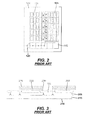
- FIG. 2 shows an interline charge-coupled device (CCD) 100. It includes an array of photodiodes 105 connected to vertical CCD 110 (VCCD). The image readout process begins by transferring charge from the photodiodes 105 to the adjacent VCCDs 110. Next, one line at a time is transferred into the horizontal CCD (HCCD) 115. The HCCD serially transfers charge to an output charge-sensing amplifier 120.
- CCD interline charge-coupled device
- FIG. 3 shows a cross section of one interline CCD pixel (with portions of adjacent pixels shown for clarity) of Fig. 2 .
- the photodiode 105 collects photo-generated charge. The charge is confined in the photodiode 105 by a surface pinning p+ implant 230 and a vertical overflow drain 215. Adjacent to the photodiode 105 is the VCCD buried channel 200 built in a p-type well 205 on an n-type substrate 210. Transfer of charge through the VCCD 110 is controlled by the gate 220. The VCCD 110 is shielded from light by an opaque metal layer 225.
- the overflow drain 215 is a lightly doped region that has a high degree of manufacturing process variability. The variability is so great that the voltage applied to the substrate 210 must by changed from one image sensor to the next.
- the substrate voltage controls how much charge can be held in the photodiode 105. If the charge capacity of the photodiode is too high, then a bright spot of light will generate more charge than can be held in the VCCD 110. This causes VCCD blooming. If the charge capacity is too low, then the output amplifier 120 will never reach saturation.
- the substrate voltage is adjusted for each individual image sensor to optimize the photodiode charge capacity for the best compromise between anti-blooming protection and saturation signal level.
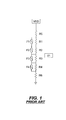
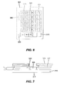
- FIG. 1 This circuit contains four fuses, F1 through F4, across a set of resistors in series, R1 through R4. By blowing one or more of the fuses, 16 possible reference voltage combinations V1 are possible. This reference voltage is then connected to the image sensor substrate for optimum anti-blooming and saturation signal.
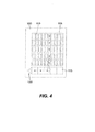
- FIG. 4 A simple example is shown in Figure 4 .
- An interline CCD 100 is shown where two rows of charge from the VCCD 110 is summed into the HCCD 115. This summing process may cause the HCCD 115 charge capacity to be exceeded and result in horizontal charge blooming. It is also possible to sum pixels together in the VCCD to increase frame rates. The pixel summing in the VCCD may exceed the VCCD charge capacity.
- a well-known solution to prevent blooming of the VCCD or HCCD when summing pixels is to further increase the substrate voltage when in pixel summing mode.
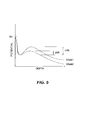
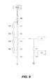
- Figure 5 illustrates the photodiode 105 channel potential vs. depth in the silicon wafer.
- the pinning layer 230 holds the potential at 0V.
- the n-type photodiode 105 and lightly doped overflow drain 215 form a potential barrier between the photodiode and substrate 210.
- the substrate voltage is set to VSub1
- the photodiode capacity is larger at ⁇ VB.
- the image sensor changes to pixel summing mode, then the substrate voltage is increased to VSub2 which lowers the photodiode charge capacity to ⁇ VA.
- the problem is how to generate a second reference voltage.
- the obvious solution would be to place an entire second reference voltage generator on the image sensor like that shown in Figure 1 . This is undesirable because adding more fuses to the image sensor requires extra bond pads for a wafer probe tester to be able to set the fuses. Even if laser trimmed fuses are used, the additional fuses decrease the manufacturing yield of the sensor and increases the chance of debris from the fuse setting process contaminating the pixel array. Therefore, a new circuit is needed that does not increase the number of fuses and can supply more than one reference voltage for pixel summing image sensors.
- the present invention is directed to overcoming one or more of the problems set forth above. Briefly summarized, according to one aspect of the present invention, the invention resides in an image sensor according to claim 1.
- the present invention provides the advantage of a simple image sensor substrate voltage circuit that can supply multiple substrate reference voltages without increasing the number of programmable fuse elements.
- FIG. 6 shows an interline CCD image sensor 300 of the present invention with an integrated substrate reference voltage circuit 360 of the invention on the same silicon substrate.
- the image sensor 300 has an array of pixels 304 consisting of a photodiode 305, which collects charge in response to incident light (i.e., photons), adjacent to a vertical CCD shift register 310 that receives charge from the photodiodes.
- a horizontal CCD shift register 315 receives charge from the vertical CCD shift registers 310 and serially transfers charge to an output charge sensing node 320.
- the vertical CCD 310 is capable of summing together charge from two or more photodiodes 305 within the vertical CCD 310.
- Figure 7 shows a horizontal cross section of one of the pixels 304. It consists of an n-type photodiode 305 under a p-type surface pinning layer 330 and above the lightly doped vertical overflow drain 316 in the n-type substrate 317.
- the opaque light shield 303 prevents the CCD shift register buried channel 302 from being sensitive to light.
- An equivalent image sensor can have all of the silicon doping polarities (n-type and p-type) exchanged.
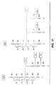
- FIG. 8 shows the relationship between the optimum substrate voltage for two pixel summing vs. the optimum substrate voltage for no pixel summing. It is a straight line intersecting the origin.
- Figure 9 shows a circuit that will produce a second voltage V2 that can reproduce the straight line in Figure 8 .
- V1 and V2 set by the fuses F1 through F4 can be calculated.
- V2 is the optimum substrate voltage for the full resolution un-summed image and
- V1 is the optimum substrate voltage for two pixel summing.
- F1 through F4 are values of 1 or 0 depending if the fuse F1 through F4 is conducting current or is blown.
- V1 and V2 have a linear relationship and an intercept through the origin.
- the circuit of Figure 9 uses the same number of fuses as the prior art but provides two reference voltage of exactly the correct value for pixel summing and non-pixel summing modes.
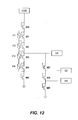
- Interline CCDs are not limited to summing only 2 pixels. It is possible for one sensor to have multiple levels of pixel summing. For example, an image sensor might take full resolution pictures and also have video modes with 2, 4, or 8 pixel summing. Odd numbered pixel summing is also possible such as a color image sensor with the Bayer color filter pattern summing 3x3 (9 pixel) subarrays of like colors. All of these pixel-summing modes will need reference voltages on one image sensor.
- the solution is to extend the circuit of Figure 9 to the circuit shown in Figure 10 where another voltage divider operating off the V2 voltage generates a third voltage V3.
- Figure 11 shows two variations of the circuit in Figure 10 that can generate a third voltage V3. From, these examples it should be clear how to add an unlimited number of additional voltage dividers to generate more substrate voltage references.
- FET field effect transistors
- FIG. 13 Another variation is shown in Figure 13 .
- anti-fuses AF1 through AF4 have replaced the fuses.
- a fuse is initially a conductive link and then an external stimulus such as a high current pulse or laser-cutting beam is used to open the conductive link.
- the anti-fuse is initially an open link that is then fused together by an external stimulus such as a high voltage that breaks down an insulating layer between two conducting plates.
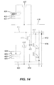
- FIG. 14 shows two CMOS image sensor pixels.
- the photodiodes have a surface pinning layer 424 and a vertical overflow drain 422.
- the charge capacity of the photodiodes 426 and 423 is regulated by the overflow drain 422 barrier height that is in turn controlled by the voltage applied to the substrate 421.
- Charge from the photodiode 426 is transferred to a shared floating diffusion 425 by a transfer gate 427 controlled by the signal line 428.
- Charge from the photodiode 423 is transferred to a floating a shared floating diffusion 425 by a transfer gate 414 controlled by the signal line 419.
- Each photodiode signal charge can be read either by transferring independently to the floating diffusion 425 or in a pixel summing operation both transfer gates 414 and 427 are turned on at the same time to sum two pixels together.
- the floating diffusion 425 is reset by transistor 413 controlled by signal line 411.
- Transistor 417 is preferably a part of a source follower connected to a power line 412.
- Transistor 418 is a row select transistor turned on by signal line 420 to connect the source follower to the signal output line 416.
- CMOS pixel structure allows two-pixel summing or no pixel summing read out modes. It can also be extended to allow for 3 or 4 pixel summing options. In the case of pixel summing is it desirable to use the overflow drain reference voltage circuit invention to supply reference voltages for each of the pixel summing modes.
- Figure 15 shows a camera imaging system 471 (preferably a digital camera) employing an image sensor 470 with the integrated overflow drain voltage reference circuit of the present invention.
- the present invention permits the digital camera system 471 to operate in full resolution picture taking modes as well as lower resolution pixel summed motion video imaging modes with optimal anti-blooming protection and saturation signal level.
Landscapes
- Engineering & Computer Science (AREA)
- Multimedia (AREA)
- Signal Processing (AREA)
- Transforming Light Signals Into Electric Signals (AREA)
- Solid State Image Pick-Up Elements (AREA)
Applications Claiming Priority (2)
| Application Number | Priority Date | Filing Date | Title |
|---|---|---|---|
| US11/488,961 US7508432B2 (en) | 2006-07-19 | 2006-07-19 | CCD with improved substrate voltage setting circuit |
| PCT/US2007/016280 WO2008011064A2 (en) | 2006-07-19 | 2007-07-18 | Ccd with improved substrate voltage setting circuit |
Publications (2)
| Publication Number | Publication Date |
|---|---|
| EP2041958A2 EP2041958A2 (en) | 2009-04-01 |
| EP2041958B1 true EP2041958B1 (en) | 2015-10-21 |
Family
ID=38957346
Family Applications (1)
| Application Number | Title | Priority Date | Filing Date |
|---|---|---|---|
| EP07810576.4A Active EP2041958B1 (en) | 2006-07-19 | 2007-07-18 | Ccd with improved substrate voltage setting circuit |
Country Status (4)
| Country | Link |
|---|---|
| US (1) | US7508432B2 (enExample) |
| EP (1) | EP2041958B1 (enExample) |
| JP (1) | JP4982562B2 (enExample) |
| WO (1) | WO2008011064A2 (enExample) |
Families Citing this family (11)
| Publication number | Priority date | Publication date | Assignee | Title |
|---|---|---|---|---|
| US7508432B2 (en) * | 2006-07-19 | 2009-03-24 | Eastman Kodak Company | CCD with improved substrate voltage setting circuit |
| JPWO2009128194A1 (ja) * | 2008-04-16 | 2011-08-04 | パナソニック株式会社 | 固体撮像装置、撮像システム、及び固体撮像装置の駆動方法 |
| EP2133918B1 (en) | 2008-06-09 | 2015-01-28 | Sony Corporation | Solid-state imaging device, drive method thereof and electronic apparatus |
| US20100149379A1 (en) * | 2008-12-16 | 2010-06-17 | Summa Joseph R | Image sensor with three-dimensional interconnect and ccd |
| JP5404112B2 (ja) * | 2009-03-12 | 2014-01-29 | キヤノン株式会社 | 固体撮像素子、その駆動方法及び撮像システム |
| JP5302073B2 (ja) * | 2009-04-01 | 2013-10-02 | 浜松ホトニクス株式会社 | 固体撮像装置 |
| US8736924B2 (en) * | 2011-09-28 | 2014-05-27 | Truesense Imaging, Inc. | Time-delay-and-integrate image sensors having variable integration times |
| US9462202B2 (en) | 2013-06-06 | 2016-10-04 | Samsung Electronics Co., Ltd. | Pixel arrays and imaging devices with reduced blooming, controllers and methods |
| CN105161045B (zh) * | 2015-10-21 | 2018-06-29 | 京东方科技集团股份有限公司 | 栅极集成驱动电路、其修复方法、显示面板及显示装置 |
| RU2699805C1 (ru) * | 2018-10-08 | 2019-09-11 | Вячеслав Михайлович Смелков | Способ управления чувствительностью телевизионной камеры на матрице ПЗС и воспроизведения её видеосигнала в составе мобильного устройства в условиях сложной освещённости и/или сложной яркости объектов |
| RU2699813C1 (ru) * | 2018-11-13 | 2019-09-11 | Вячеслав Михайлович Смелков | Способ управления чувствительностью телевизионной камеры на матрице ПЗС в условиях сложной освещённости и/или сложной яркости объектов, компьютерной регистрации видеосигнала и его воспроизведения |
Family Cites Families (31)
| Publication number | Priority date | Publication date | Assignee | Title |
|---|---|---|---|---|
| JPH02309877A (ja) * | 1989-05-25 | 1990-12-25 | Sony Corp | 固体撮像装置 |
| JP2601933B2 (ja) | 1990-04-13 | 1997-04-23 | 株式会社東芝 | 固体撮像装置 |
| JP2725714B2 (ja) * | 1991-01-04 | 1998-03-11 | シャープ株式会社 | Ccd固体撮像素子 |
| JP3113406B2 (ja) * | 1992-08-13 | 2000-11-27 | 旭光学工業株式会社 | スチルビデオカメラの撮像素子制御装置 |
| JPH06153079A (ja) | 1992-11-12 | 1994-05-31 | Sony Corp | Ccd固体撮像素子 |
| US5978024A (en) * | 1994-04-15 | 1999-11-02 | Lg Semicon Co., Ltd. | Auto variable anti-blooming bias control circuit and method |
| US5786852A (en) * | 1994-06-20 | 1998-07-28 | Canon Kabushiki Kaisha | Image pick-up apparatus having an image sensing device including a photoelectric conversion part and a vertical transfer part |
| JP3635681B2 (ja) * | 1994-07-15 | 2005-04-06 | ソニー株式会社 | バイアス回路の調整方法、電荷転送装置、及び電荷検出装置とその調整方法 |
| JP3701992B2 (ja) * | 1994-09-12 | 2005-10-05 | 富士写真フイルム株式会社 | ライン・イメージ・センサの出力映像信号処理装置および方法 |
| JPH0955473A (ja) | 1995-06-08 | 1997-02-25 | Matsushita Electron Corp | 半導体装置とその検査方法 |
| JP3847811B2 (ja) * | 1995-06-30 | 2006-11-22 | キヤノン株式会社 | 撮像装置 |
| JPH09139486A (ja) * | 1995-11-16 | 1997-05-27 | Sony Corp | 固体撮像素子及び固体撮像素子の駆動方法 |
| EP2259568A3 (en) | 1996-09-20 | 2011-06-22 | Sony Corporation | Solid-state imaging apparatus, driving method therefor, and camera |
| JP3440722B2 (ja) * | 1996-09-20 | 2003-08-25 | ソニー株式会社 | 固体撮像装置およびその駆動方法並びにカメラ |
| JP2000133791A (ja) * | 1998-10-26 | 2000-05-12 | Sony Corp | 固体撮像装置 |
| JP3296312B2 (ja) | 1999-01-06 | 2002-06-24 | 日本電気株式会社 | 固体撮像装置およびその製造方法 |
| JP2000236475A (ja) * | 1999-02-16 | 2000-08-29 | Canon Inc | 撮像装置 |
| JP4320835B2 (ja) * | 1999-04-16 | 2009-08-26 | ソニー株式会社 | 固体撮像装置およびその駆動方法並びにカメラシステム |
| JP3928837B2 (ja) * | 1999-09-13 | 2007-06-13 | 株式会社ルネサステクノロジ | 半導体集積回路装置 |
| US7102680B2 (en) | 2000-03-13 | 2006-09-05 | Olympus Corporation | Image pickup device capable of adjusting the overflow level of the sensor based on the read out mode |
| JP2002231889A (ja) | 2001-01-31 | 2002-08-16 | Sony Corp | バイアス発生装置 |
| JP3878575B2 (ja) * | 2003-04-28 | 2007-02-07 | 松下電器産業株式会社 | 固体撮像装置及びその駆動方法 |
| JP2005006201A (ja) * | 2003-06-13 | 2005-01-06 | Matsushita Electric Ind Co Ltd | 固体撮像装置 |
| JP4309737B2 (ja) * | 2003-10-03 | 2009-08-05 | パナソニック株式会社 | 撮像素子を駆動する駆動装置 |
| JP2005123965A (ja) * | 2003-10-17 | 2005-05-12 | Fuji Film Microdevices Co Ltd | 固体撮像装置 |
| JP2005277398A (ja) * | 2004-02-25 | 2005-10-06 | Sony Corp | Ccdリニアセンサ |
| JP2005260407A (ja) * | 2004-03-10 | 2005-09-22 | Fuji Photo Film Co Ltd | 撮像素子の読出制御装置および撮影装置 |
| US7385638B2 (en) | 2004-04-28 | 2008-06-10 | Eastman Kodak Company | Image sensor for still or video photography |
| JP2007036609A (ja) * | 2005-07-26 | 2007-02-08 | Matsushita Electric Ind Co Ltd | 固体撮像装置の駆動方法および固体撮像装置 |
| US7982790B2 (en) * | 2006-01-16 | 2011-07-19 | Panasonic Corporation | Solid-state imaging apparatus and method for driving the same |
| US7508432B2 (en) * | 2006-07-19 | 2009-03-24 | Eastman Kodak Company | CCD with improved substrate voltage setting circuit |
-
2006
- 2006-07-19 US US11/488,961 patent/US7508432B2/en active Active
-
2007
- 2007-07-18 WO PCT/US2007/016280 patent/WO2008011064A2/en not_active Ceased
- 2007-07-18 EP EP07810576.4A patent/EP2041958B1/en active Active
- 2007-07-18 JP JP2009520819A patent/JP4982562B2/ja active Active
Also Published As
| Publication number | Publication date |
|---|---|
| WO2008011064A3 (en) | 2008-05-08 |
| US7508432B2 (en) | 2009-03-24 |
| EP2041958A2 (en) | 2009-04-01 |
| JP4982562B2 (ja) | 2012-07-25 |
| JP2009544230A (ja) | 2009-12-10 |
| WO2008011064A2 (en) | 2008-01-24 |
| US20080017892A1 (en) | 2008-01-24 |
Similar Documents
| Publication | Publication Date | Title |
|---|---|---|
| EP2041958B1 (en) | Ccd with improved substrate voltage setting circuit | |
| EP0862219B1 (en) | Active pixel sensor in which adjacent pixels share an integrated electrical element | |
| EP0913869B1 (en) | Active pixel sensor with programmable color balance | |
| US11532653B2 (en) | Imaging device | |
| KR970007711B1 (ko) | 오버-플로우 드레인(ofd)구조를 가지는 전하결합소자형 고체촬상장치 | |
| US20050128327A1 (en) | Device and method for image sensing | |
| US5430481A (en) | Multimode frame transfer image sensor | |
| JP2004221585A (ja) | リセットノイズ抑制及びプログラム可能ビニング能力を備えたaps画素 | |
| KR101575378B1 (ko) | 고체 촬상 장치 및 이를 포함하는 x선 ct 장치 | |
| KR100265269B1 (ko) | 수직 오버플로우 드레인 및 저항성 게이트 전하 전송소자를 가지는 고체촬상소자 및 그 제어방법 | |
| JP2009026984A (ja) | 固体撮像素子 | |
| KR101254832B1 (ko) | 이미지 센서 및 이를 포함하는 카메라 | |
| JP2005057772A (ja) | クロック式障壁を備えたバーチャル・フェーズccdイメージ・センサー | |
| EP0453530B1 (en) | Solid-state image sensor | |
| KR20140003418A (ko) | 고체 촬상 장치 | |
| Janesick et al. | Scientific CMOS pixels | |
| EP0216426A1 (en) | Imaging devices comprising photovoltaic detector elements | |
| KR100801758B1 (ko) | 이미지 센서 및 그 제어 방법 | |
| JP4326021B2 (ja) | 電荷結合撮像装置 | |
| EP0215531A1 (en) | Imaging devices comprising photodetector elements | |
| US5047862A (en) | Solid-state imager | |
| Bosiers et al. | A 35-mm format 11 M pixel full-frame CCD for professional digital still imaging | |
| JP2003224255A (ja) | 固体撮像素子およびこれを用いた撮像装置 | |
| Beynon | Optical self-scanned arrays. Part 1: Principles of self-scanned arrays | |
| KR19990018938A (ko) | 전하 결합 소자형 이미지 센서 |
Legal Events
| Date | Code | Title | Description |
|---|---|---|---|
| PUAI | Public reference made under article 153(3) epc to a published international application that has entered the european phase |
Free format text: ORIGINAL CODE: 0009012 |
|
| 17P | Request for examination filed |
Effective date: 20090109 |
|
| AK | Designated contracting states |
Kind code of ref document: A2 Designated state(s): AT BE BG CH CY CZ DE DK EE ES FI FR GB GR HU IE IS IT LI LT LU LV MC MT NL PL PT RO SE SI SK TR |
|
| AX | Request for extension of the european patent |
Extension state: AL BA HR MK RS |
|
| DAX | Request for extension of the european patent (deleted) | ||
| RBV | Designated contracting states (corrected) |
Designated state(s): DE FR GB NL |
|
| RAP1 | Party data changed (applicant data changed or rights of an application transferred) |
Owner name: OMNIVISION TECHNOLOGIES, INC. |
|
| 17Q | First examination report despatched |
Effective date: 20140701 |
|
| GRAP | Despatch of communication of intention to grant a patent |
Free format text: ORIGINAL CODE: EPIDOSNIGR1 |
|
| INTG | Intention to grant announced |
Effective date: 20150616 |
|
| GRAS | Grant fee paid |
Free format text: ORIGINAL CODE: EPIDOSNIGR3 |
|
| GRAA | (expected) grant |
Free format text: ORIGINAL CODE: 0009210 |
|
| AK | Designated contracting states |
Kind code of ref document: B1 Designated state(s): DE FR GB NL |
|
| REG | Reference to a national code |
Ref country code: GB Ref legal event code: FG4D |
|
| REG | Reference to a national code |
Ref country code: DE Ref legal event code: R096 Ref document number: 602007043608 Country of ref document: DE |
|
| REG | Reference to a national code |
Ref country code: NL Ref legal event code: FP |
|
| REG | Reference to a national code |
Ref country code: FR Ref legal event code: PLFP Year of fee payment: 10 |
|
| REG | Reference to a national code |
Ref country code: DE Ref legal event code: R097 Ref document number: 602007043608 Country of ref document: DE |
|
| PLBE | No opposition filed within time limit |
Free format text: ORIGINAL CODE: 0009261 |
|
| STAA | Information on the status of an ep patent application or granted ep patent |
Free format text: STATUS: NO OPPOSITION FILED WITHIN TIME LIMIT |
|
| 26N | No opposition filed |
Effective date: 20160722 |
|
| REG | Reference to a national code |
Ref country code: FR Ref legal event code: PLFP Year of fee payment: 11 |
|
| REG | Reference to a national code |
Ref country code: FR Ref legal event code: PLFP Year of fee payment: 12 |
|
| REG | Reference to a national code |
Ref country code: DE Ref legal event code: R079 Ref document number: 602007043608 Country of ref document: DE Free format text: PREVIOUS MAIN CLASS: H04N0005335000 Ipc: H04N0025000000 |
|
| PGFP | Annual fee paid to national office [announced via postgrant information from national office to epo] |
Ref country code: GB Payment date: 20250612 Year of fee payment: 19 |
|
| PGFP | Annual fee paid to national office [announced via postgrant information from national office to epo] |
Ref country code: NL Payment date: 20250618 Year of fee payment: 19 |
|
| PGFP | Annual fee paid to national office [announced via postgrant information from national office to epo] |
Ref country code: FR Payment date: 20250612 Year of fee payment: 19 |
|
| PGFP | Annual fee paid to national office [announced via postgrant information from national office to epo] |
Ref country code: DE Payment date: 20250616 Year of fee payment: 19 |