EP2008769B1 - Polishing apparatus and polishing method - Google Patents
Polishing apparatus and polishing method Download PDFInfo
- Publication number
- EP2008769B1 EP2008769B1 EP08011343A EP08011343A EP2008769B1 EP 2008769 B1 EP2008769 B1 EP 2008769B1 EP 08011343 A EP08011343 A EP 08011343A EP 08011343 A EP08011343 A EP 08011343A EP 2008769 B1 EP2008769 B1 EP 2008769B1
- Authority
- EP
- European Patent Office
- Prior art keywords
- polishing
- tape
- substrate
- polishing head
- head
- Prior art date
- Legal status (The legal status is an assumption and is not a legal conclusion. Google has not performed a legal analysis and makes no representation as to the accuracy of the status listed.)
- Active
Links
Images


Classifications
-
- B—PERFORMING OPERATIONS; TRANSPORTING
- B24—GRINDING; POLISHING
- B24B—MACHINES, DEVICES, OR PROCESSES FOR GRINDING OR POLISHING; DRESSING OR CONDITIONING OF ABRADING SURFACES; FEEDING OF GRINDING, POLISHING, OR LAPPING AGENTS
- B24B21/00—Machines or devices using grinding or polishing belts; Accessories therefor
- B24B21/002—Machines or devices using grinding or polishing belts; Accessories therefor for grinding edges or bevels
-
- B—PERFORMING OPERATIONS; TRANSPORTING
- B24—GRINDING; POLISHING
- B24B—MACHINES, DEVICES, OR PROCESSES FOR GRINDING OR POLISHING; DRESSING OR CONDITIONING OF ABRADING SURFACES; FEEDING OF GRINDING, POLISHING, OR LAPPING AGENTS
- B24B9/00—Machines or devices designed for grinding edges or bevels on work or for removing burrs; Accessories therefor
- B24B9/02—Machines or devices designed for grinding edges or bevels on work or for removing burrs; Accessories therefor characterised by a special design with respect to properties of materials specific to articles to be ground
- B24B9/06—Machines or devices designed for grinding edges or bevels on work or for removing burrs; Accessories therefor characterised by a special design with respect to properties of materials specific to articles to be ground of non-metallic inorganic material, e.g. stone, ceramics, porcelain
-
- B—PERFORMING OPERATIONS; TRANSPORTING
- B24—GRINDING; POLISHING
- B24B—MACHINES, DEVICES, OR PROCESSES FOR GRINDING OR POLISHING; DRESSING OR CONDITIONING OF ABRADING SURFACES; FEEDING OF GRINDING, POLISHING, OR LAPPING AGENTS
- B24B21/00—Machines or devices using grinding or polishing belts; Accessories therefor
- B24B21/16—Machines or devices using grinding or polishing belts; Accessories therefor for grinding other surfaces of particular shape
-
- B—PERFORMING OPERATIONS; TRANSPORTING
- B24—GRINDING; POLISHING
- B24B—MACHINES, DEVICES, OR PROCESSES FOR GRINDING OR POLISHING; DRESSING OR CONDITIONING OF ABRADING SURFACES; FEEDING OF GRINDING, POLISHING, OR LAPPING AGENTS
- B24B9/00—Machines or devices designed for grinding edges or bevels on work or for removing burrs; Accessories therefor
- B24B9/02—Machines or devices designed for grinding edges or bevels on work or for removing burrs; Accessories therefor characterised by a special design with respect to properties of materials specific to articles to be ground
- B24B9/06—Machines or devices designed for grinding edges or bevels on work or for removing burrs; Accessories therefor characterised by a special design with respect to properties of materials specific to articles to be ground of non-metallic inorganic material, e.g. stone, ceramics, porcelain
- B24B9/065—Machines or devices designed for grinding edges or bevels on work or for removing burrs; Accessories therefor characterised by a special design with respect to properties of materials specific to articles to be ground of non-metallic inorganic material, e.g. stone, ceramics, porcelain of thin, brittle parts, e.g. semiconductors, wafers
-
- H—ELECTRICITY
- H01—ELECTRIC ELEMENTS
- H01L—SEMICONDUCTOR DEVICES NOT COVERED BY CLASS H10
- H01L21/00—Processes or apparatus adapted for the manufacture or treatment of semiconductor or solid state devices or of parts thereof
- H01L21/67—Apparatus specially adapted for handling semiconductor or electric solid state devices during manufacture or treatment thereof; Apparatus specially adapted for handling wafers during manufacture or treatment of semiconductor or electric solid state devices or components ; Apparatus not specifically provided for elsewhere
- H01L21/683—Apparatus specially adapted for handling semiconductor or electric solid state devices during manufacture or treatment thereof; Apparatus specially adapted for handling wafers during manufacture or treatment of semiconductor or electric solid state devices or components ; Apparatus not specifically provided for elsewhere for supporting or gripping
- H01L21/687—Apparatus specially adapted for handling semiconductor or electric solid state devices during manufacture or treatment thereof; Apparatus specially adapted for handling wafers during manufacture or treatment of semiconductor or electric solid state devices or components ; Apparatus not specifically provided for elsewhere for supporting or gripping using mechanical means, e.g. chucks, clamps or pinches
- H01L21/68707—Apparatus specially adapted for handling semiconductor or electric solid state devices during manufacture or treatment thereof; Apparatus specially adapted for handling wafers during manufacture or treatment of semiconductor or electric solid state devices or components ; Apparatus not specifically provided for elsewhere for supporting or gripping using mechanical means, e.g. chucks, clamps or pinches the wafers being placed on a robot blade, or gripped by a gripper for conveyance
-
- H—ELECTRICITY
- H01—ELECTRIC ELEMENTS
- H01L—SEMICONDUCTOR DEVICES NOT COVERED BY CLASS H10
- H01L21/00—Processes or apparatus adapted for the manufacture or treatment of semiconductor or solid state devices or of parts thereof
- H01L21/67—Apparatus specially adapted for handling semiconductor or electric solid state devices during manufacture or treatment thereof; Apparatus specially adapted for handling wafers during manufacture or treatment of semiconductor or electric solid state devices or components ; Apparatus not specifically provided for elsewhere
- H01L21/683—Apparatus specially adapted for handling semiconductor or electric solid state devices during manufacture or treatment thereof; Apparatus specially adapted for handling wafers during manufacture or treatment of semiconductor or electric solid state devices or components ; Apparatus not specifically provided for elsewhere for supporting or gripping
- H01L21/687—Apparatus specially adapted for handling semiconductor or electric solid state devices during manufacture or treatment thereof; Apparatus specially adapted for handling wafers during manufacture or treatment of semiconductor or electric solid state devices or components ; Apparatus not specifically provided for elsewhere for supporting or gripping using mechanical means, e.g. chucks, clamps or pinches
- H01L21/68714—Apparatus specially adapted for handling semiconductor or electric solid state devices during manufacture or treatment thereof; Apparatus specially adapted for handling wafers during manufacture or treatment of semiconductor or electric solid state devices or components ; Apparatus not specifically provided for elsewhere for supporting or gripping using mechanical means, e.g. chucks, clamps or pinches the wafers being placed on a susceptor, stage or support
- H01L21/68792—Apparatus specially adapted for handling semiconductor or electric solid state devices during manufacture or treatment thereof; Apparatus specially adapted for handling wafers during manufacture or treatment of semiconductor or electric solid state devices or components ; Apparatus not specifically provided for elsewhere for supporting or gripping using mechanical means, e.g. chucks, clamps or pinches the wafers being placed on a susceptor, stage or support characterised by the construction of the shaft
Definitions
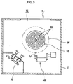
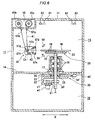
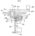
- the polishing tape 141 After contacting the periphery of the wafer W, the polishing tape 141 is rewound by the rewind reel 145b.
- the supply reel 145a and the rewind reel 145b are coupled to non-illustrated motors that provide the polishing tape 141 with a suitable tension.
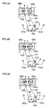
- the polishing head 142 performs a linearly-reciprocating motion in vertical directions, as indicated by arrows in FIG 1 , to thereby provide relative movement between the polishing tape 141 and the wafer W, thus polishing the periphery of the wafer W
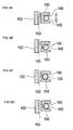
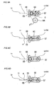
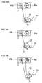
- FIG 4A shows a state in which a center Ch of the polishing head 142 is aligned with a thickness center Cw of the wafer W (which will be hereinafter referred to as simply a wafer center).
- the wafer center Cw is fixed in position during polishing.
- the polishing head 142 performs the linearly-reciprocating motion across the wafer center Cw.
- the pivot of the swinging motion is positioned in the polishing head.
- the polishing tape 41 may comprise a base film having a polishing surface to which abrasive particles, such as diamond particles or SiC particles, are attached.
- the abrasive particles to be attached to the polishing tape 41 are selected in accordance with a type of wafer and a polishing performance required.
- the abrasive particles may be diamond particles or SiC particles having an average diameter in a range of 0.1 ⁇ m to 5.0 ⁇ m.
- the polishing tape 42 may be a belt-shaped polishing cloth with no abrasive particles.
- the base film may comprise a film made from a flexible material, such as polyester, polyurethane, or polyethylene terephthalate.
Landscapes
- Engineering & Computer Science (AREA)
- Mechanical Engineering (AREA)
- General Physics & Mathematics (AREA)
- Manufacturing & Machinery (AREA)
- Power Engineering (AREA)
- Microelectronics & Electronic Packaging (AREA)
- Physics & Mathematics (AREA)
- Condensed Matter Physics & Semiconductors (AREA)
- Computer Hardware Design (AREA)
- Inorganic Chemistry (AREA)
- Chemical & Material Sciences (AREA)
- Ceramic Engineering (AREA)
- Robotics (AREA)
- Finish Polishing, Edge Sharpening, And Grinding By Specific Grinding Devices (AREA)
- Mechanical Treatment Of Semiconductor (AREA)
- Grinding And Polishing Of Tertiary Curved Surfaces And Surfaces With Complex Shapes (AREA)
Applications Claiming Priority (1)
| Application Number | Priority Date | Filing Date | Title |
|---|---|---|---|
| JP2007171959 | 2007-06-29 |
Publications (2)
| Publication Number | Publication Date |
|---|---|
| EP2008769A1 EP2008769A1 (en) | 2008-12-31 |
| EP2008769B1 true EP2008769B1 (en) | 2011-03-02 |
Family
ID=39816648
Family Applications (1)
| Application Number | Title | Priority Date | Filing Date |
|---|---|---|---|
| EP08011343A Active EP2008769B1 (en) | 2007-06-29 | 2008-06-23 | Polishing apparatus and polishing method |
Country Status (7)
| Country | Link |
|---|---|
| US (1) | US7976361B2 (ja) |
| EP (1) | EP2008769B1 (ja) |
| JP (2) | JP5188285B2 (ja) |
| KR (1) | KR101488993B1 (ja) |
| CN (1) | CN101332580B (ja) |
| DE (1) | DE602008005211D1 (ja) |
| TW (1) | TWI436852B (ja) |
Families Citing this family (21)
| Publication number | Priority date | Publication date | Assignee | Title |
|---|---|---|---|---|
| US8892238B2 (en) * | 2009-10-06 | 2014-11-18 | Edward T. Sweet | Edge break details and processing |
| US20110081839A1 (en) * | 2009-10-06 | 2011-04-07 | Apple Inc. | Method and apparatus for polishing a curved edge |
| JP5182317B2 (ja) * | 2010-03-31 | 2013-04-17 | ブラザー工業株式会社 | レンズ |
| CN101934489B (zh) * | 2010-07-30 | 2012-10-03 | 溧阳市四方不锈钢制品有限公司 | 管坯焊缝打磨机 |
| JP5649417B2 (ja) * | 2010-11-26 | 2015-01-07 | 株式会社荏原製作所 | 固定砥粒を有する研磨テープを用いた基板の研磨方法 |
| US8540551B2 (en) * | 2010-12-15 | 2013-09-24 | Corning Incorporated | Glass edge finish system, belt assembly, and method for using same |
| CN102233536A (zh) * | 2011-05-10 | 2011-11-09 | 淄博隆嘉工贸有限公司 | 陶瓷手模自动抛光机 |
| TWI590915B (zh) * | 2012-09-24 | 2017-07-11 | Ebara Corp | Grinding method |
| US9339912B2 (en) | 2013-01-31 | 2016-05-17 | Taiwan Semiconductor Manufacturing Company, Ltd. | Wafer polishing tool using abrasive tape |
| JP6071611B2 (ja) * | 2013-02-13 | 2017-02-01 | Mipox株式会社 | オリエンテーションフラット等切り欠き部を有する、結晶材料から成るウエハの周縁を、研磨テープを使用して研磨することにより円形ウエハを製造する方法 |
| JP2015000451A (ja) * | 2013-06-17 | 2015-01-05 | ワイエイシイ株式会社 | 基板表面加工装置 |
| JP6113624B2 (ja) * | 2013-10-11 | 2017-04-12 | 株式会社荏原製作所 | 基板処理装置および基板処理方法 |
| CN105196140B (zh) * | 2015-10-20 | 2017-05-31 | 慈溪市华表机械有限公司 | 一种外圆超精机 |
| EP3335832B1 (en) * | 2016-12-15 | 2021-02-03 | Ebara Corporation | Polishing apparatus and pressing pad for pressing polishing tool |
| JP6920849B2 (ja) * | 2017-03-27 | 2021-08-18 | 株式会社荏原製作所 | 基板処理方法および装置 |
| JP6974067B2 (ja) * | 2017-08-17 | 2021-12-01 | 株式会社荏原製作所 | 基板を研磨する方法および装置 |
| JP7129166B2 (ja) * | 2018-01-11 | 2022-09-01 | 株式会社荏原製作所 | 基板処理装置及び制御方法 |
| JP7226711B2 (ja) * | 2019-02-28 | 2023-02-21 | 範多機械株式会社 | 斫り装置 |
| CN111745504B (zh) * | 2020-05-20 | 2022-06-21 | 深圳市裕展精密科技有限公司 | 打磨机构、打磨装置及打磨方法 |
| CN111941201B (zh) * | 2020-08-21 | 2021-12-07 | 许昌学院 | 一种用于法布里-珀罗干涉仪镜板的高精度制造装置 |
| CN114619338A (zh) * | 2022-03-28 | 2022-06-14 | 坦龙环保设备南通有限公司 | 一种扫地车液压杆生产装置 |
Family Cites Families (20)
| Publication number | Priority date | Publication date | Assignee | Title |
|---|---|---|---|---|
| JP2837342B2 (ja) * | 1993-12-13 | 1998-12-16 | 日本ミクロコーティング株式会社 | 研磨装置 |
| JP3081140B2 (ja) | 1995-09-21 | 2000-08-28 | 日本ミクロコーティング株式会社 | 研磨テープによる研磨装置 |
| NO306765B1 (no) * | 1998-04-03 | 1999-12-20 | Grobi As | Anordning for kantrunding av hull i et arbeidsstykke |
| US6685539B1 (en) * | 1999-08-24 | 2004-02-03 | Ricoh Company, Ltd. | Processing tool, method of producing tool, processing method and processing apparatus |
| US6629875B2 (en) * | 2000-01-28 | 2003-10-07 | Accretech Usa, Inc. | Machine for grinding-polishing of a water edge |
| JP4156200B2 (ja) * | 2001-01-09 | 2008-09-24 | 株式会社荏原製作所 | 研磨装置及び研磨方法 |
| JP2003220546A (ja) * | 2002-01-24 | 2003-08-05 | Soken Kogyo Kk | ベルト式研磨装置 |
| JP4090247B2 (ja) * | 2002-02-12 | 2008-05-28 | 株式会社荏原製作所 | 基板処理装置 |
| JP4125148B2 (ja) | 2003-02-03 | 2008-07-30 | 株式会社荏原製作所 | 基板処理装置 |
| EP1719161B1 (en) * | 2004-02-25 | 2014-05-07 | Ebara Corporation | Polishing apparatus |
| US7744445B2 (en) * | 2004-10-15 | 2010-06-29 | Kabushiki Kaisha Toshiba | Polishing apparatus and polishing method |
| JP2006142388A (ja) * | 2004-11-16 | 2006-06-08 | Nihon Micro Coating Co Ltd | 研磨テープ及び方法 |
| US20090017733A1 (en) * | 2005-04-19 | 2009-01-15 | Ebara Corporation | Substrate processing apparatus |
| KR101203505B1 (ko) | 2005-04-19 | 2012-11-21 | 가부시키가이샤 에바라 세이사꾸쇼 | 기판 처리 장치 및 기판 처리 방법 |
| JP5196709B2 (ja) * | 2005-04-19 | 2013-05-15 | 株式会社荏原製作所 | 半導体ウエハ周縁研磨装置及び方法 |
| US7993485B2 (en) * | 2005-12-09 | 2011-08-09 | Applied Materials, Inc. | Methods and apparatus for processing a substrate |
| WO2007070353A2 (en) * | 2005-12-09 | 2007-06-21 | Applied Materials, Inc. | Methods and apparatus for processing a substrate |
| WO2007126815A2 (en) * | 2006-03-30 | 2007-11-08 | Applied Materials, Inc. | Methods and apparatus for polishing an edge of a subtrate |
| JP2008036783A (ja) * | 2006-08-08 | 2008-02-21 | Sony Corp | 研磨方法および研磨装置 |
| JP2008284684A (ja) * | 2007-05-21 | 2008-11-27 | Applied Materials Inc | 研磨アームを使用して基板の縁部を研磨する方法及び装置 |
-
2008
- 2008-06-16 US US12/213,186 patent/US7976361B2/en active Active
- 2008-06-19 JP JP2008160380A patent/JP5188285B2/ja active Active
- 2008-06-19 TW TW097122820A patent/TWI436852B/zh active
- 2008-06-23 EP EP08011343A patent/EP2008769B1/en active Active
- 2008-06-23 DE DE602008005211T patent/DE602008005211D1/de active Active
- 2008-06-27 CN CN2008101285883A patent/CN101332580B/zh active Active
- 2008-06-27 KR KR20080061705A patent/KR101488993B1/ko active IP Right Grant
-
2012
- 2012-12-14 JP JP2012273699A patent/JP5525590B2/ja active Active
Also Published As
| Publication number | Publication date |
|---|---|
| TWI436852B (zh) | 2014-05-11 |
| JP2009028892A (ja) | 2009-02-12 |
| DE602008005211D1 (de) | 2011-04-14 |
| JP2013075358A (ja) | 2013-04-25 |
| KR20090004590A (ko) | 2009-01-12 |
| US7976361B2 (en) | 2011-07-12 |
| CN101332580A (zh) | 2008-12-31 |
| KR101488993B1 (ko) | 2015-02-02 |
| CN101332580B (zh) | 2012-05-09 |
| JP5525590B2 (ja) | 2014-06-18 |
| EP2008769A1 (en) | 2008-12-31 |
| TW200932423A (en) | 2009-08-01 |
| US20090004952A1 (en) | 2009-01-01 |
| JP5188285B2 (ja) | 2013-04-24 |
Similar Documents
| Publication | Publication Date | Title |
|---|---|---|
| EP2008769B1 (en) | Polishing apparatus and polishing method | |
| US9457447B2 (en) | Polishing apparatus and polishing method | |
| US8393935B2 (en) | Polishing apparatus | |
| EP2502701B1 (en) | Polishing apparatus and polishing method | |
| US8047896B2 (en) | Polishing apparatus, polishing method, and processing apparatus | |
| US10414013B2 (en) | Polishing method and polishing apparatus | |
| JP2009154285A (ja) | 研磨装置および研磨方法 | |
| US20080293334A1 (en) | Methods and apparatus for using a bevel polishing head with an efficient tape routing arrangement | |
| TWI820076B (zh) | 基板處理裝置以及控制方法 | |
| TWI433754B (zh) | 研磨裝置 | |
| US6638147B2 (en) | Polishing method for removing corner material from a semi-conductor wafer | |
| JPH0976148A (ja) | ウェーハのノッチ部研磨装置 | |
| JP3404579B2 (ja) | 両端軸状部研磨装置 | |
| JP3542815B2 (ja) | ウェハーノッチ部の鏡面研磨装置およびその鏡面研磨方法 | |
| JP3888618B2 (ja) | ロッド端面加工装置 | |
| JP7296864B2 (ja) | 研磨装置および研磨方法 | |
| WO2009011408A1 (ja) | 研磨装置 | |
| JPH1040508A (ja) | 磁気ヘッド摺動面加工装置及び磁気ヘッド摺動面加工方法 | |
| JP2004174629A (ja) | 金属ベルトリングの面取り装置 | |
| JP2004243470A (ja) | ワークの面取り装置 | |
| JP5360726B2 (ja) | 板状部材研磨装置 | |
| JP2003007657A (ja) | ウェハノッチの鏡面研磨装置及び鏡面研磨方法 | |
| JP2000005997A (ja) | ウェーハの加工方法及びその装置 |
Legal Events
| Date | Code | Title | Description |
|---|---|---|---|
| PUAI | Public reference made under article 153(3) epc to a published international application that has entered the european phase |
Free format text: ORIGINAL CODE: 0009012 |
|
| AK | Designated contracting states |
Kind code of ref document: A1 Designated state(s): AT BE BG CH CY CZ DE DK EE ES FI FR GB GR HR HU IE IS IT LI LT LU LV MC MT NL NO PL PT RO SE SI SK TR |
|
| AX | Request for extension of the european patent |
Extension state: AL BA MK RS |
|
| 17P | Request for examination filed |
Effective date: 20090624 |
|
| 17Q | First examination report despatched |
Effective date: 20090722 |
|
| AKX | Designation fees paid |
Designated state(s): DE |
|
| GRAP | Despatch of communication of intention to grant a patent |
Free format text: ORIGINAL CODE: EPIDOSNIGR1 |
|
| GRAS | Grant fee paid |
Free format text: ORIGINAL CODE: EPIDOSNIGR3 |
|
| GRAA | (expected) grant |
Free format text: ORIGINAL CODE: 0009210 |
|
| AK | Designated contracting states |
Kind code of ref document: B1 Designated state(s): DE |
|
| REF | Corresponds to: |
Ref document number: 602008005211 Country of ref document: DE Date of ref document: 20110414 Kind code of ref document: P |
|
| REG | Reference to a national code |
Ref country code: DE Ref legal event code: R096 Ref document number: 602008005211 Country of ref document: DE Effective date: 20110414 |
|
| PLBE | No opposition filed within time limit |
Free format text: ORIGINAL CODE: 0009261 |
|
| STAA | Information on the status of an ep patent application or granted ep patent |
Free format text: STATUS: NO OPPOSITION FILED WITHIN TIME LIMIT |
|
| 26N | No opposition filed |
Effective date: 20111205 |
|
| REG | Reference to a national code |
Ref country code: DE Ref legal event code: R097 Ref document number: 602008005211 Country of ref document: DE Effective date: 20111205 |
|
| P01 | Opt-out of the competence of the unified patent court (upc) registered |
Effective date: 20230517 |
|
| PGFP | Annual fee paid to national office [announced via postgrant information from national office to epo] |
Ref country code: DE Payment date: 20230502 Year of fee payment: 16 |