EP1968104A2 - Halbleiterbauelement und Verfahren zu seiner Herstellung - Google Patents
Halbleiterbauelement und Verfahren zu seiner Herstellung Download PDFInfo
- Publication number
- EP1968104A2 EP1968104A2 EP08011174A EP08011174A EP1968104A2 EP 1968104 A2 EP1968104 A2 EP 1968104A2 EP 08011174 A EP08011174 A EP 08011174A EP 08011174 A EP08011174 A EP 08011174A EP 1968104 A2 EP1968104 A2 EP 1968104A2
- Authority
- EP
- European Patent Office
- Prior art keywords
- region
- layer
- electrode
- sic
- semiconductor device
- Prior art date
- Legal status (The legal status is an assumption and is not a legal conclusion. Google has not performed a legal analysis and makes no representation as to the accuracy of the status listed.)
- Withdrawn
Links
Images


Classifications
-
- H—ELECTRICITY
- H10—SEMICONDUCTOR DEVICES; ELECTRIC SOLID-STATE DEVICES NOT OTHERWISE PROVIDED FOR
- H10D—INORGANIC ELECTRIC SEMICONDUCTOR DEVICES
- H10D30/00—Field-effect transistors [FET]
- H10D30/60—Insulated-gate field-effect transistors [IGFET]
- H10D30/64—Double-diffused metal-oxide semiconductor [DMOS] FETs
- H10D30/66—Vertical DMOS [VDMOS] FETs
- H10D30/668—Vertical DMOS [VDMOS] FETs having trench gate electrodes, e.g. UMOS transistors
-
- H—ELECTRICITY
- H10—SEMICONDUCTOR DEVICES; ELECTRIC SOLID-STATE DEVICES NOT OTHERWISE PROVIDED FOR
- H10D—INORGANIC ELECTRIC SEMICONDUCTOR DEVICES
- H10D12/00—Bipolar devices controlled by the field effect, e.g. insulated-gate bipolar transistors [IGBT]
- H10D12/01—Manufacture or treatment
- H10D12/031—Manufacture or treatment of IGBTs
-
- H—ELECTRICITY
- H10—SEMICONDUCTOR DEVICES; ELECTRIC SOLID-STATE DEVICES NOT OTHERWISE PROVIDED FOR
- H10D—INORGANIC ELECTRIC SEMICONDUCTOR DEVICES
- H10D30/00—Field-effect transistors [FET]
- H10D30/60—Insulated-gate field-effect transistors [IGFET]
- H10D30/63—Vertical IGFETs
- H10D30/635—Vertical IGFETs having no inversion channels, e.g. vertical accumulation channel FETs [ACCUFET] or normally-on vertical IGFETs
-
- H—ELECTRICITY
- H10—SEMICONDUCTOR DEVICES; ELECTRIC SOLID-STATE DEVICES NOT OTHERWISE PROVIDED FOR
- H10D—INORGANIC ELECTRIC SEMICONDUCTOR DEVICES
- H10D30/00—Field-effect transistors [FET]
- H10D30/60—Insulated-gate field-effect transistors [IGFET]
- H10D30/637—Lateral IGFETs having no inversion channels, e.g. buried channel lateral IGFETs, normally-on lateral IGFETs or depletion-mode lateral IGFETs
-
- H—ELECTRICITY
- H10—SEMICONDUCTOR DEVICES; ELECTRIC SOLID-STATE DEVICES NOT OTHERWISE PROVIDED FOR
- H10D—INORGANIC ELECTRIC SEMICONDUCTOR DEVICES
- H10D30/00—Field-effect transistors [FET]
- H10D30/80—FETs having rectifying junction gate electrodes
- H10D30/87—FETs having Schottky gate electrodes, e.g. metal-semiconductor FETs [MESFET]
-
- H—ELECTRICITY
- H10—SEMICONDUCTOR DEVICES; ELECTRIC SOLID-STATE DEVICES NOT OTHERWISE PROVIDED FOR
- H10D—INORGANIC ELECTRIC SEMICONDUCTOR DEVICES
- H10D62/00—Semiconductor bodies, or regions thereof, of devices having potential barriers
- H10D62/10—Shapes, relative sizes or dispositions of the regions of the semiconductor bodies; Shapes of the semiconductor bodies
- H10D62/17—Semiconductor regions connected to electrodes not carrying current to be rectified, amplified or switched, e.g. channel regions
- H10D62/213—Channel regions of field-effect devices
- H10D62/221—Channel regions of field-effect devices of FETs
- H10D62/228—Channel regions of field-effect devices of FETs having delta-doped channels
-
- H—ELECTRICITY
- H10—SEMICONDUCTOR DEVICES; ELECTRIC SOLID-STATE DEVICES NOT OTHERWISE PROVIDED FOR
- H10D—INORGANIC ELECTRIC SEMICONDUCTOR DEVICES
- H10D62/00—Semiconductor bodies, or regions thereof, of devices having potential barriers
- H10D62/80—Semiconductor bodies, or regions thereof, of devices having potential barriers characterised by the materials
- H10D62/83—Semiconductor bodies, or regions thereof, of devices having potential barriers characterised by the materials being Group IV materials, e.g. B-doped Si or undoped Ge
- H10D62/832—Semiconductor bodies, or regions thereof, of devices having potential barriers characterised by the materials being Group IV materials, e.g. B-doped Si or undoped Ge being Group IV materials comprising two or more elements, e.g. SiGe
- H10D62/8325—Silicon carbide
-
- H—ELECTRICITY
- H10—SEMICONDUCTOR DEVICES; ELECTRIC SOLID-STATE DEVICES NOT OTHERWISE PROVIDED FOR
- H10D—INORGANIC ELECTRIC SEMICONDUCTOR DEVICES
- H10D64/00—Electrodes of devices having potential barriers
- H10D64/01—Manufacture or treatment
- H10D64/011—Manufacture or treatment of electrodes ohmically coupled to a semiconductor
- H10D64/0111—Manufacture or treatment of electrodes ohmically coupled to a semiconductor to Group IV semiconductors
- H10D64/0115—Manufacture or treatment of electrodes ohmically coupled to a semiconductor to Group IV semiconductors to silicon carbide
-
- H—ELECTRICITY
- H10—SEMICONDUCTOR DEVICES; ELECTRIC SOLID-STATE DEVICES NOT OTHERWISE PROVIDED FOR
- H10D—INORGANIC ELECTRIC SEMICONDUCTOR DEVICES
- H10D8/00—Diodes
- H10D8/60—Schottky-barrier diodes
-
- H—ELECTRICITY
- H10—SEMICONDUCTOR DEVICES; ELECTRIC SOLID-STATE DEVICES NOT OTHERWISE PROVIDED FOR
- H10D—INORGANIC ELECTRIC SEMICONDUCTOR DEVICES
- H10D84/00—Integrated devices formed in or on semiconductor substrates that comprise only semiconducting layers, e.g. on Si wafers or on GaAs-on-Si wafers
- H10D84/01—Manufacture or treatment
- H10D84/02—Manufacture or treatment characterised by using material-based technologies
- H10D84/03—Manufacture or treatment characterised by using material-based technologies using Group IV technology, e.g. silicon technology or silicon-carbide [SiC] technology
- H10D84/035—Manufacture or treatment characterised by using material-based technologies using Group IV technology, e.g. silicon technology or silicon-carbide [SiC] technology using silicon carbide [SiC] technology
-
- H—ELECTRICITY
- H10—SEMICONDUCTOR DEVICES; ELECTRIC SOLID-STATE DEVICES NOT OTHERWISE PROVIDED FOR
- H10D—INORGANIC ELECTRIC SEMICONDUCTOR DEVICES
- H10D84/00—Integrated devices formed in or on semiconductor substrates that comprise only semiconducting layers, e.g. on Si wafers or on GaAs-on-Si wafers
- H10D84/80—Integrated devices formed in or on semiconductor substrates that comprise only semiconducting layers, e.g. on Si wafers or on GaAs-on-Si wafers characterised by the integration of at least one component covered by groups H10D12/00 or H10D30/00, e.g. integration of IGFETs
- H10D84/811—Combinations of field-effect devices and one or more diodes, capacitors or resistors
-
- H—ELECTRICITY
- H10—SEMICONDUCTOR DEVICES; ELECTRIC SOLID-STATE DEVICES NOT OTHERWISE PROVIDED FOR
- H10D—INORGANIC ELECTRIC SEMICONDUCTOR DEVICES
- H10D62/00—Semiconductor bodies, or regions thereof, of devices having potential barriers
- H10D62/10—Shapes, relative sizes or dispositions of the regions of the semiconductor bodies; Shapes of the semiconductor bodies
- H10D62/17—Semiconductor regions connected to electrodes not carrying current to be rectified, amplified or switched, e.g. channel regions
- H10D62/213—Channel regions of field-effect devices
- H10D62/221—Channel regions of field-effect devices of FETs
- H10D62/235—Channel regions of field-effect devices of FETs of IGFETs
- H10D62/314—Channel regions of field-effect devices of FETs of IGFETs having vertical doping variations
-
- H—ELECTRICITY
- H10—SEMICONDUCTOR DEVICES; ELECTRIC SOLID-STATE DEVICES NOT OTHERWISE PROVIDED FOR
- H10D—INORGANIC ELECTRIC SEMICONDUCTOR DEVICES
- H10D62/00—Semiconductor bodies, or regions thereof, of devices having potential barriers
- H10D62/60—Impurity distributions or concentrations
- H10D62/605—Planar doped, e.g. atomic-plane doped or delta-doped
-
- H—ELECTRICITY
- H10—SEMICONDUCTOR DEVICES; ELECTRIC SOLID-STATE DEVICES NOT OTHERWISE PROVIDED FOR
- H10D—INORGANIC ELECTRIC SEMICONDUCTOR DEVICES
- H10D64/00—Electrodes of devices having potential barriers
- H10D64/20—Electrodes characterised by their shapes, relative sizes or dispositions
- H10D64/23—Electrodes carrying the current to be rectified, amplified, oscillated or switched, e.g. sources, drains, anodes or cathodes
- H10D64/251—Source or drain electrodes for field-effect devices
- H10D64/256—Source or drain electrodes for field-effect devices for lateral devices wherein the source or drain electrodes are recessed in semiconductor bodies
-
- H—ELECTRICITY
- H10—SEMICONDUCTOR DEVICES; ELECTRIC SOLID-STATE DEVICES NOT OTHERWISE PROVIDED FOR
- H10D—INORGANIC ELECTRIC SEMICONDUCTOR DEVICES
- H10D84/00—Integrated devices formed in or on semiconductor substrates that comprise only semiconducting layers, e.g. on Si wafers or on GaAs-on-Si wafers
- H10D84/01—Manufacture or treatment
-
- Y—GENERAL TAGGING OF NEW TECHNOLOGICAL DEVELOPMENTS; GENERAL TAGGING OF CROSS-SECTIONAL TECHNOLOGIES SPANNING OVER SEVERAL SECTIONS OF THE IPC; TECHNICAL SUBJECTS COVERED BY FORMER USPC CROSS-REFERENCE ART COLLECTIONS [XRACs] AND DIGESTS
- Y10—TECHNICAL SUBJECTS COVERED BY FORMER USPC
- Y10S—TECHNICAL SUBJECTS COVERED BY FORMER USPC CROSS-REFERENCE ART COLLECTIONS [XRACs] AND DIGESTS
- Y10S438/00—Semiconductor device manufacturing: process
- Y10S438/931—Silicon carbide semiconductor
Definitions
- the present invention relates to a semiconductor device formed using a compound semiconductor layer, and more particularly relates to a semiconductor device suitable for applications requiring a high breakdown voltage or a large current, and a method for fabricating the same.
- silicon carbide semiconductors have a dielectric breakdown electric field ten times greater than silicon, and thus can maintain a relatively high reverse breakdown voltage in spite of a narrow depletion layer of a pn junction or a Schottky junction.
- silicon carbide semiconductors are expected to be materials for power devices having a low on-state resistance, a high breakdown voltage and low loss. This is because they can be used to reduce the thickness of the semiconductor layer and enhance the doping concentration.
- Figure 15 is a cross sectional view showing a double-implanted, accumulation-mode MISFET (ACCUFET) using SiC, which is suggested by the present inventors in Document 1 (see Osamu Kusumoto and the other 6 persons, "SiC Vertical DACFET", Materials Science Forum, No. 389-393, pp. 1211-1214 ).
- ACCUFET accumulation-mode MISFET
- the known accumulation-mode MISFET comprises a low-resistance SiC substrate 1001, a high-resistance SiC layer 1002 that is epitaxially grown on the SiC substrate 1001 and has a higher resistance than the SiC substrate 1001, a p-well region 1003 formed by selectively implanting ions into the surface region of the high-resistance SiC layer 1002, an accumulation channel layer 1004 formed on the surface region of the p-well region 1003 and including a multiple ⁇ -doped layer formed by alternately stacking many ⁇ -doped layers and undoped layers, and a source region 1006 formed by implanting ions into a part of the accumulation channel layer 1004 and containing an n-type impurity at a high concentration.
- a gate insulating film 1008 is formed over the accumulation channel layer 1004 and a part of the source region 1006, and a gate electrode 1010 is formed on the gate insulating film 1008.
- a part of the source region 1006 is removed to form a recess, and the well region 1003 is partly exposed at the bottom of the recess.
- a contact layer 1005 containing a p-type impurity at a high concentration is formed on the bottom of the recess, and a source electrode 1011 is provided on the contact layer 1005 to fill the recess and extend to the top of the source region 1006.
- the source electrode 1011 makes an ohmic contact with the source region 1006 and the contact layer 1005 by heat treatment.
- a drain electrode 1012 is formed on the back surface of the SiC substrate 1001 to make an ohmic contact with the SiC substrate 1001.
- the n-type dopant concentration in the high-resistance SiC layer 1002 is usually about 1x10 15 cm -3 through 3x10 16 cm -3 .
- This dopant concentration depends on a desired breakdown voltage. That is, this dopant concentration becomes lower with the increase of the desired breakdown voltage.
- the accumulation channel layer 1004 When the accumulation channel layer 1004 has a certain level of high impurity concentration, the channel resistance becomes low. However, in this case, the breakdown voltage decreases. The reason for this is that a depletion layer at the surface of the high-resistance SiC layer 1002 does not extend. That is, there is a trade-off relationship between high breakdown voltage and low loss. Therefore, the impurity concentration in the accumulation channel layer cannot be high.
- nickel is often used for an ohmic electrode of an n-type silicon carbide semiconductor, and the nickel ohmic electrode is subjected to annealing at 900°C or higher in an atmosphere of an inert gas, such as argon or nitrogen.
- an inert gas such as argon or nitrogen.
- the source electrode 1011 needs to directly contact the contact layer 1005, because the contact layer 1005, which is a heavily-doped p-type layer, applies a bias to the well region 1003. To cope with this, a recess is formed in the source region 1006 and the source electrode 1011 is formed along the wall surface of the recess. As a result, a voltage is directly applied from the source electrode 1011 to the contact layer 1005.
- the structure of the known semiconductor device has the following problems.
- Silicon carbide has a large binding energy between carbon and silicon. This makes it difficult to clear crystal defects formed therein due to ion implantation.
- the dose of ions is also large. In this case, defects may cause troubles. Therefore, ions need to be implanted with the substrate kept at a high temperature of 500°C or higher, and the temperature of activation annealing after the implantation needs to be set at a high temperature of 1400°C or higher. In turn, the fabrication process is complicated, resulting in increased cost.
- the annealing temperature needs to be high.
- silicon is selectively evaporated from the surface of SiC to form pits or cause step bunching, and flatness of the surface is degraded.
- the present invention is made to solve these problems, and its object is to realize a semiconductor device which keeps the contact resistance of a source electrode low without forming a source region by ion implantation and has a high breakdown voltage and low loss.
- a semiconductor device of the present invention may comprise: a substrate; an active region composed of a compound semiconductor provided on the substrate, said active region being obtained by alternately stacking at least one first semiconductor layer serving as a region through which carriers flow and at least two second semiconductor layers that contain an impurity for carriers at a higher concentration than the first semiconductor layer and are thinner than the first semiconductor layer; and at least one electrode of a conductor material entering into the active region from the top side to contact at least each of the second semiconductor layers.
- a semiconductor device serving as a transistor or a diode allowing carriers to flow through the active region composed of a compound semiconductor can be realized. Accordingly, for semiconductor devices using compound semiconductors and having high performance such as high power and high breakdown voltage, their fabrication cost can be reduced.
- the semiconductor device may further comprise: a gate insulating film provided on the active region; and a gate electrode provided on the gate insulting film.
- the semiconductor device serves as a MISFET. In this case, it can also serve as an accumulation-mode MISFET.
- the semiconductor device may further comprise: a Schottky gate electrode provided on the active region.
- a Schottky gate electrode provided on the active region.
- the semiconductor device serves as a MESFET.
- the semiconductor device may further comprise: a Schottky gate electrode making a Schottky contact with the active region.
- a Schottky gate electrode making a Schottky contact with the active region.
- the compound semiconductor layer is a SiC layer
- ion implantation requiring a large amount of labor particularly for the SiC layer need not be performed while advantage is taken of a large band gap. Therefore, the effect of reduction in fabrication cost becomes remarkable.
- the at least one electrode is preferably composed of a conductor material containing at least nickel.
- a method for fabricating a semiconductor device of the present invention using a part of a semiconductor layer provided on a substrate as an active region may comprise the steps of: (a) forming an active region in which at least one first semiconductor layer and at least two second semiconductor layers are alternately stacked, said second semiconductor layers containing an impurity for carriers at a higher concentration than the first semiconductor layer and being thinner than the first semiconductor layer; (b) depositing a conductor film on the active region and then patterning the deposited conductor film in the form of an electrode; and (c) subjecting the conductor film to annealing after the step (b), thereby forming an electrode that enters into the active region from the surface thereof to contact at least each of the second semiconductor layers.
- a semiconductor device having an active region through which a large amount of carriers flow at a high speed can be obtained in the step (c) without ion implantation steps. More particularly, for semiconductor devices using compound semiconductors and having high performance such as high power and high breakdown voltage, their fabrication cost can be reduced.
- the electrode is preferably brought into an ohmic contact with at least each of the second semiconductor layers.
- the conductor film contains at least nickel and in the step (c), the annealing is carried out at a high temperature of 600°C or higher in an atmosphere of an inert gas.
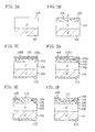
- Figure 1 is a cross sectional view showing a double-implanted, accumulation-mode MISFET (ACCUFET) using SiC according to a first embodiment of the present invention.
- ACCUFET accumulation-mode MISFET
- an accumulation-mode MISFET of this first embodiment comprises a low-resistance SiC substrate 101, a high-resistance SiC layer 102 that is epitaxially grown on the SiC substrate 101 and has a higher resistance than the SiC substrate 101, a p-type well region 103 formed by selectively implanting ions into the surface region of the high-resistance SiC layer 102, an n-type accumulation channel layer 104 having a multiple ⁇ -doped layer (active region) formed on the surface region of the well region 103, and a contact layer 105 formed by implanting a p-type impurity at a high concentration into the well region 103.
- a gate insulating film 108 is formed on the accumulation channel layer 104, and a gate electrode 110 is formed on the gate insulating film 108. Furthermore, a drain electrode 112 is formed on the back surface of the SiC substrate 101 to make an ohmic contact with the SiC substrate 101.
- the accumulation channel layer 104 has a structure in which two undoped layers 104b (first semiconductor layers) of about 40nm thickness composed of undoped SiC single crystals and two ⁇ -doped layers 104a (second semiconductor layers) of about 10nm thickness having a peak concentration of an n-type impurity of 5 ⁇ 10 17 cm -3 , are alternately stacked, and an undoped layer 104b of about 40nm thickness is further stacked thereon.
- the ⁇ -doped layer 104a is formed sufficiently thin to allow spreading movement of carriers to the undoped layer 104b under a quantum effect.
- the ⁇ -doped layer 104a is obtained using a crystal growing device and a crystal growing method both disclosed in the specifications and drawings of Japanese Patent Applications No. 2000-58964 and 2000-06210 . Effects and benefits brought by the provision of this multiple ⁇ -doped layer are as disclosed in Japanese Patent Applications No. 2002-500456 and 2001-566193 .
- This embodiment is characterized in that a source electrode 111 is provided which enters into the accumulation channel layer 104 and the contact layer 105 by reaction with SiC and comes into direct contact with the contact layer 105. There is formed no source region that would conventionally have been formed by implanting impurities into the accumulation channel layer 104 and the well region 103 at high concentration.
- the source electrode 111 is composed of a nickel silicide layer obtained by sequentially forming an accumulation channel layer 104 and a nickel layer thereon and then allowing nickel to react with SiC by annealing. During this annealing, nickel enters into the accumulation channel layer 104 and the contact layer 105 principally by diffusion.
- the source electrode 111 substantially makes an ohmic contact with the ⁇ -doped layer 104a located in the accumulation channel layer 104, and also substantially makes an ohmic contact with the contact layer 105.
- the depth to which nickel enters into these layers after annealing can be adjusted in accordance with the initial thickness of the nickel film and annealing conditions.
- Figure 2A is a diagram schematically showing the relationship between the concentration profile of nitrogen that is an n-type impurity and carrier profile in the depthwise direction of a multiple ⁇ -doped layer
- Figure 2B is a partial band diagram showing the shape of a conduction band edge along the depthwise direction.
- the conduction band edge of the whole active region has a shape connecting the conduction band edge of the ⁇ -doped layer and the conduction band edge of the undoped layer, both shown by the broken lines in this figure. More particularly, quantum levels resulting from a quantum effect occur in the ⁇ -doped layer 104a, and the wave function of electrons localized in the ⁇ -doped layer 104a expands to a certain degree.
- the breakdown voltage is defined by the undoped layer 104b of low impurity concentration, so that a high breakdown voltage can be obtained in the entire accumulation channel layer 104. Accordingly, in the ACCUFET having a structure in which the accumulation channel layer 104 is utilized to pass a large current between the source and drain, a high channel mobility and a high breakdown voltage can be achieved at the same time. In the state where the entire accumulation channel layer is depleted, as a matter of course, carriers are not present in the undoped layer and the ⁇ -doped layer. Accordingly, the ACCUFET exhibits a high breakdown voltage.
- the fabrication process can be simplified. Since SiC is a very hard material, ions need to be implanted with high energy while implantation energy is changed many times, resulting in a large amount of labor required. However, according to this embodiment, the ion implantation step for forming the source region can be saved, leading to a simplified fabrication process and reduced fabrication cost.
- a bias can be supplied from the source electrode 111 through the contact region 105 to the well region 103 even without forming a recess. Since SiC is a very hard material, a large amount of labor is required for etching. However, according to this embodiment, the etching step for forming the source electrode can be saved, leading to a simplified fabrication process and reduced fabrication cost.
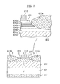
- Figures 3A through 3F are cross sectional views showing process steps for fabricating a semiconductor device according to the first embodiment.
- a SiC substrate 101 is prepared in which the surface inclined at an angle of 8° from the (0001) plane in the ⁇ 11-20> direction ((0001) off plane) provides the principal surface and the doping concentration of an n-type impurity (nitrogen) is approximately 1 ⁇ 10 18 cm -3 through 5 ⁇ 10 19 cm -3 .
- a high-resistance SiC layer 102 is epitaxially grown thereon.
- the high-resistance SiC layer 102 is epitaxially grown to contain a lower concentration of an impurity (dopant) than the SiC substrate 101 by thermal chemical-vapor deposition (CVD), e.g., using silane and propane as source gases, hydrogen as a carrier gas, and nitrogen gas as a dopant gas.
- CVD thermal chemical-vapor deposition
- the dopant concentration of the high-resistance SiC layer 102 ranges from 1 ⁇ 10 15 cm -3 to 1 ⁇ 10 16 cm -3 and its thickness is 10 ⁇ m or more.
- ions of aluminum (Al) or boron (B) that are p-type impurities are implanted into a part of the high-resistance SiC layer 102 to form a well region 103.
- a silicon oxide film (not shown) of approximately 3 ⁇ m thickness serving as an implantation mask is deposited on the high-resistance SiC layer 102 by CVD or the like. Then, a part of the silicon oxide film in which the well region 103 is to be formed is opened by photolithography and dry etching.
- ions of Al or B are implanted into the opened part of the silicon oxide film with the substrate temperature kept at a high temperature of 500°C or higher. After this ion implantation, the silicon oxide film is totally removed by hydrofluoric acid.
- the dopant concentration in the well region 103 usually ranges approximately from 1 ⁇ 10 17 cm -3 to 1 ⁇ 10 18 cm -3 , and its depth is around 1 ⁇ m such that the well region 103 does not pinch off.
- ions of a p-type impurity (Al or B) are implanted into the surface part of the well region 103 at a high concentration, thereby forming a contact region 105 of a p + type.
- the thickness of the contact region 105 is around 300nm, and its doping concentration is 1 ⁇ 10 18 cm -3 or more.
- ion implantation is carried out like the well region 103.
- activation annealing is performed in an inert gas, such as argon, at around 1700°C for approximately half an hour.
- a multiple ⁇ -doped layer 104x serving as a channel of a MISFET is formed on the surfaces of the high-resistance SiC layer 102, the well region 103 and the contact region 105.
- the multiple ⁇ -doped layer 104x has a structure in which two 40nm-thick undoped layers 104b (first semiconductor layers) and two 10nm-thick ⁇ -doped layers 104a (second semiconductor layers) having a peak concentration of an n-type dopant of 1 ⁇ 10 18 cm -3 , are alternately stacked, and a 40nm-thick undoped layer 104b is further stacked thereon.
- a crystal growing device and a crystal growing method both disclosed in Japanese Patent Application No. 2001-566193 are used to fabricate such a structure. More particularly, a SiC substrate is placed in a growth furnace for thermal CVD, hydrogen and argon are allowed to flow therethrough as diluent gases, and propane gas and silane gas are introduced into the growth furnace as source gases. The inside of the growth furnace is kept at a pressure of 0.0933MPa, and the substrate temperature is adjusted at 1600°C. In this state, 40nm-thick undoped layers are epitaxially grown.
- a doped layer In order to form a doped layer, not only the above-mentioned diluent gases and source gases are supplied into the growth furnace, but also nitrogen is pulsatingly supplied as a doping gas thereinto. In such a state, 10nm-thick ⁇ -doped layers 104a are epitaxially grown. The dopant concentration is controlled by adjusting the on/off time width or duty ratio of each pulse of a pulse valve. With this method, a multiple ⁇ -doped layer 104x is formed by alternately depositing three undoped layers 104b and two ⁇ -doped layers 104a.
- the surface of the multiple ⁇ -doped layer 104x (undoped layer 104b) is thermally oxidized, thereby forming a silicon oxide film 108x.
- the SiC substrate is placed in a quartz tube, bubbled oxygen is introduced into the quartz tube at a flow rate of 2.5 (1/min), and thermal oxidation is carried out for three hours with the substrate temperature kept at 1100°C. As a result, a thermal oxide film is formed to have a thickness of approximately 40nm.
- a 200nm-thick drain electrode 112 composed of a nickel film is formed on the back surface of the SiC substrate 101 by vapor deposition.
- the drain electrode 112 is subjected to annealing after the later formation of a source electrode.
- a resist film (not shown) having an opened region where a source electrode is to be formed is formed on the silicon oxide film 108x by photolithography. Thereafter, the silicon oxide film 108x is patterned by hydrofluoric acid etching to form a gate insulating film 108 to surround the region where a source electrode is to be formed. Next, a 200nm-thick nickel film (Ni film) is successively deposited on the substrate by vacuum deposition or the like with the resist film left. Thereafter, a nickel film 111x is left by a lift-off technique.
- Ni film nickel film
- the Ni film 111x is subjected to annealing, for example, in the atmosphere of an inert gas, such as nitrogen, at a temperature of 1000°C for two minutes. During this annealing, interdiffusion and reaction are caused between nickel (Ni) and silicon carbide (SiC), thereby forming a source electrode 111 principally composed of nickel silicide. Then, a part of the multiple ⁇ -doped layer 104x which is not integrated into the source electrode 111 forms an accumulation channel layer 104.
- an inert gas such as nitrogen
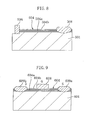
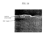
- Figure 14 is a SEM (scanning electron microscope) photographic view showing the structures of the source electrode formed in the step shown in Figure 3E and an underlying SiC layer. As shown in this figure, it is found that the source electrode is embedded into the substrate from the substrate surface to a depth of approximately 200nm. Although a multiple ⁇ -doped layer is not formed in a sample of which this SEM photograph was taken, it is found that the source electrode 111 composed of nickel silicide can be sufficiently brought into contact with the contact region 105 . The reason for this is that the thickness of the multiple ⁇ -doped layer 104x in this embodiment is 140nm.
- an aluminum film is deposited on the substrate by vapor deposition, and thereafter the aluminum film is patterned by photolithography and wet etching, thereby forming a gate electrode 110 on the gate insulating film 108 .
- an implantation mask composed of a silicon oxide film or the like is formed on the substrate to cover the substrate except the region thereof into which n-type impurity ions are to be implanted and open the region. Thereafter, the substrate is heated to have a temperature of 500 through 800°C, and nitrogen ions (N + ) or the like are implanted into the substrate from above the implantation mask. Furthermore, annealing for impurity activation is performed at a temperature of 1500°C for half an hour.
- a heavily-doped ion implantation layer is formed to have an n-type impurity concentration of about 1 ⁇ 10 18 atoms ⁇ cm -3 .
- nitrogen ions (N + ) are implanted into the substrate, for example, in six ion implantation process steps with different implantation energies.
- the conditions for the first ion implantation are an acceleration voltage of 180keV and a dose amount of 1.5 ⁇ 10 14 atoms ⁇ cm -2
- the conditions for the second ion implantation are an acceleration voltage of 130keV and a dose amount of 1 ⁇ 10 14 atoms ⁇ cm -2
- the conditions for the third ion implantation are an acceleration voltage of 110keV and a dose amount of 5 ⁇ 10 13 atoms ⁇ cm -2
- the conditions for the fourth ion implantation are an acceleration voltage of 100keV and a dose amount of 8 ⁇ 10 13 atoms ⁇ cm -2
- the conditions for the fifth ion implantation are an acceleration voltage of 60keV and a dose amount of 6 ⁇ 10 13 atoms ⁇ cm -2
- the conditions for the sixth ion implantation are an acceleration voltage of 30keV and a dose amount of 5 ⁇ 10 13 atoms ⁇ cm -2 .
- the depth of the ion implantation is approximately 0.3 ⁇ m.
- the ion implantation process steps in the known process for fabricating a semiconductor device have had the following problem. More particularly, the underlying SiC layer is slightly etched during the formation of the opening in the implantation mask composed of a silicon oxide film or the like. Therefore, only the source region is dented so that a step is formed therein. An electric field may have been concentrated in a gate oxide film located on such a step, leading to a breakdown voltage drop.
- an ACCUFET that is a MISFET can be formed even without the above-mentioned ion implantation process steps.
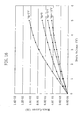
- Figure 16 is a graph showing results obtained by measuring drain current (Id) to drain voltage (Vd) characteristics (I-V characteristics) of an ACCUFET formed using a method for fabricating a semiconductor device of this embodiment.
- Data shown in Figure 16 were obtained by prototyping a sample of a double-implanted, accumulation-mode MISFET (ACCUFET) with a gate length of 2 ⁇ m and a total gate width of 1.2mm through the method for fabricating a semiconductor device of this embodiment and then actually measuring its characteristics.
- the distance between adjacent p-type well regions in the ACCUFET as a sample is 5 ⁇ m.
- a MOS operation has surely been verified in the ACCUFET formed by the method for fabricating a semiconductor device of this embodiment.
- FIG. 15 A known double-implanted, accumulation-mode MISFET (ACCUFET) shown in Figure 15 was prototyped for comparison, and then the prototyped MISFET was compared in I-V characteristics to the ACCUFET of this embodiment.
- Figure 17 is a graph showing results obtained by measuring the I-V characteristics of a known double-implanted, accumulation-mode MISFET (ACCUFET).
- the difference between the fabrication process for the known ACCUFET and the fabrication process for the ACCUFET of this embodiment is only the presence or absence of formation of a source region by ion implantation, and the other process steps of both of them are identical.
- the source region is not formed by ion implantation, there is no big change in the drain current value of the ACCUFET. It has not been recognized that the contact resistance increases between a source electrode directly provided in a channel and the channel.
- the breakdown voltage between the source and drain was 600V when the ACCUFET of this embodiment was in the off state.
- the accumulation channel layer 104 is formed of the multiple ⁇ -doped layer 104x obtained by stacking extra-thin doped layers 104a and relatively thick undoped layers 104b .
- the accumulation channel layer 104 with a high channel mobility can be obtained, because in the accumulation channel layer 104, carriers that have spread out from the ⁇ -doped layers 104a under a quantum effect or the like flow through the undoped layers 104b with a high crystallinity and small scattering by impurity ions.
- the source electrode 111 substantially makes an ohmic contact with only the ⁇ -doped layers 104a in the accumulation channel layer 104 and does not make an ohmic contact with the undoped layers 104b.
- carriers are supplied from the ⁇ -doped layers 104a to the undoped layers 104b, a sufficiently high drain current can be obtained.
- the impurity concentration in a channel layer is low.
- an ohmic contact is not formed even when the source electrode is brought into direct contact with the channel layer.
- each of the ⁇ -doped layers contains impurities at a high concentration, the source electrode can make an ohmic contact with the ⁇ -doped layers.
- Carriers are supplied from the ⁇ -doped layers to the undoped layers.
- Figure 4 is a cross sectional view showing the structure of a trench MISFET constituting a semiconductor device according to a second embodiment of the present invention.
- a trench MISFET of this second embodiment comprises a low-resistance SiC substrate 201, a high-resistance SiC layer 202 that is epitaxially grown on the SiC substrate 201 and has a higher resistance than the SiC substrate 201, a p-type base layer 203 formed by selectively implanting ions into the surface region of the high-resistance SiC layer 202, an n-type channel layer 204 having a multiple ⁇ -doped layer (active region) formed along the wall surface of a trench which passes through part of the p-type base layer 203 and reaches the high-resistance SiC layer 202, and a contact region 205 formed by implanting a p-type impurity at a high concentration into the p-type base layer 203.
- a gate insulating film 208 is formed on the channel layer 204, and a gate electrode 210 is formed on the gate insulating film 208. Furthermore, a drain electrode 212 is formed on the back surface of the SiC substrate 201 to substantially make an ohmic contact with the Si substrate 201.
- the channel layer 204 has a structure in which two undoped layers (lightly-doped layers) 204b of about 40nm thickness composed of undoped SiC single crystals and two ⁇ -doped layers (heavily-doped layers) 204a of about 10nm thickness having a peak concentration of n-type impurity of 1 ⁇ 10 18 cm -3 , are alternately stacked, and an undoped layer 204b of about 40nm thickness is stacked thereon.
- the n-type doped layers 204a are formed sufficiently thin to allow spreading movement of carriers to the undoped layers 204b under a quantum effect.
- Such a ⁇ -doped layer is obtained using a crystal growing device and a crystal growing method both disclosed in the specification and drawing of Japanese Patent Application No. 2001-566193 . Effects and benefits brought by the provision of this multiple ⁇ -doped layer are as disclosed in Japanese Patent Application No. 2002-500456 .
- This embodiment is characterized in that a source electrode 211 is provided which enters into the channel layer 204 and the contact region 205 by reaction with SiC and comes into direct contact with the contact region 205. There is formed no source region that would conventionally have been formed by implanting impurities at high concentration into the channel layer 204 and the p-type base layer 203.
- the source electrode 211 is composed of a nickel silicide layer obtained by forming an aluminum film and a nickel film on the channel layer 204 and then allowing nickel to react with SiC by annealing, and an aluminum alloy layer. During this annealing, nickel enters into the channel layer 204 and the contact region 205 principally by diffusion. Therefore, the source electrode 211 substantially makes an ohmic contact with the ⁇ -doped layer 204a located in the channel layer 204 and also makes an ohmic contact with the contact region 205.
- a source region does not have to be formed by ion implantation.
- the fabrication process for a semiconductor device can be simplified. Since SiC is a very hard material, ions need to be implanted with high energy while implantation energy is changed many times, resulting in a large amount of labor required.
- the ion implantation step for forming the source region can be saved, leading to a simplified fabrication process and reduced fabrication cost.
- a bias can be supplied from the source electrode 211 through the contact region 205 to the base layer 203 even without forming a recess. Since SiC is a very hard material, a large amount of labor is required for etching. However, according to this embodiment, the etching step for forming the source electrode can be saved, leading to a simplified fabrication process and reduced fabrication cost.
- carriers are supplied from the source electrode 211, not via the source region, directly to the ⁇ -doped layers 204a. Therefore, no problem is caused in the operation of the semiconductor device. If anything, the on-state resistance can be further reduced.
- Figure 5A through 5F are cross sectional views showing process steps for fabricating a semiconductor device according to a second embodiment.
- a SiC substrate 201 is prepared in which the surface inclined at an angle of 8° from the (0001) plane in the ⁇ 11-20> direction ((0001) off plane) provides the principal surface and the doping concentration of an n-type impurity (nitrogen) is approximately 1 ⁇ 10 18 cm -3 through 5 ⁇ 10 19 cm -3 .
- a high-resistance SiC layer 202 is epitaxially grown thereon.
- the high-resistance SiC layer 202 is epitaxially grown to contain a lower concentration of an impurity (dopant) than the SiC substrate 201 by thermal chemical-vapor deposition (CVD), for example, using silane and propane as source gases, hydrogen as a carrier gas, and a nitrogen gas as a dopant gas.
- CVD thermal chemical-vapor deposition
- silane and propane as source gases
- hydrogen as a carrier gas
- a nitrogen gas as a dopant gas.
- the dopant concentration in the high-resistance SiC layer 202 ranges from 1 ⁇ 10 15 cm -3 to 1 ⁇ 10 16 cm -3 and its thickness is 10 ⁇ m or more.
- a p-type base layer 203 is epitaxially grown by thermal CVD using silane and propane as source gases, hydrogen as a carrier gas, and trimethylaluminum (TMA) as a dopant gas.
- TMA trimethylaluminum
- the dopant concentration in the base layer 203 is approximately 2 ⁇ 10 17 cm -3 and its thickness is approximately 2 ⁇ m.
- ions of aluminum (Al) or boron (B) that are p-type impurities are implanted into a part of the base layer 203, thereby forming a heavily-doped p-type contact region 205.
- a silicon oxide film (not shown) of approximately 3 ⁇ m thickness serving as an implantation mask is deposited on the base layer 203 by CVD or the like. Then, a part of the silicon oxide film in which the contact region 205 is to be formed is opened by photolithography and dry etching.
- ions of Al or B are implanted into the opened part of the silicon oxide film with the substrate temperature kept at a high temperature of 500°C or higher. After this ion implantation, the silicon oxide film is totally removed by hydrofluoric acid. It is preferable that the depth of the contact region 205 is approximately 300nm and its dopant concentration is approximately 1 ⁇ 10 18 cm -3 . Thereafter, activation annealing is performed in an inert gas such as argon at nearly 1700°C for approximately half an hour.
- a trench 206 is formed by reactive ion etching (RIE) to pass through the base layer 203 and reach the high-resistance SiC layer 202.
- RIE reactive ion etching
- a multiple ⁇ -doped layer 204x serving as a channel of a MISFET is formed along the wall surface of the trench 206, i.e., on the surfaces of the high-resistance SiC layer 202 , the base layer 203 and the contact region 205 .
- the multiple ⁇ -doped layer 204x has a structure in which two 40nm-thick undoped layers 204b and two 10nm-thick ⁇ -doped layers 204a each having a peak concentration of an n-type dopant of 1 ⁇ 10 18 cm -3 , are alternately stacked, and a 40nm-thick undoped layer 204b is further stacked thereon.
- a crystal growing device and a crystal growing method both disclosed in the specification and drawings of Japanese Patent Application No. 2001-566193 are used to fabricate such a structure. More particularly, the SiC substrate is placed in a growth furnace for the thermal CVD, hydrogen and argon are allowed to flow therethrough as diluent gases, and propane gas and silane gas are introduced into the growth furnace as source gases. The inside of the growth furnace is kept at a pressure of 0.0933MPa, and the substrate temperature is adjusted at 1600°C. In this state, 40nm-thick undoped layers 204b are epitaxially grown.
- a doped layer In order to form a doped layer, not only the above-mentioned diluent gases and source gases are supplied into the growth furnace, but also nitrogen is pulsatingly supplied as a doping gas thereinto. In such a state, 10nm-thick ⁇ -doped layers 204a are epitaxially grown. The dopant concentration is controlled by adjusting the on/off time width or the duty ratio of each pulse of a pulse valve. With this method, a multiple ⁇ -doped layer 204x is formed by alternately depositing three undoped layers 204b and two ⁇ -doped layers 204a.
- the surface of the multiple ⁇ -doped layer 204x (undoped layer 204b) is thermally oxidized, thereby forming a silicon oxide film 208x.
- the SiC substrate is placed in a quartz tube, bubbled oxygen is introduced into the quartz tube at a flow rate of 2.5 (1/min), and thermal oxidation is carried out for three hours with the substrate temperature kept at 1100°C.
- a thermal oxide film is formed to have a thickness of approximately 40nm.
- a gate electrode 210 is formed on the silicon oxide film 208x .
- an n-type or p-type low-resistance polysilicon film is deposited on the surface of the silicon oxide film 208x , for example, by low-pressure CVD (LPCVD), using disilane and hydrogen as source gases, and phosphine or diborane as a dopant gas.
- LPCVD low-pressure CVD
- the polysilicon film is patterned by photolithography and dry etching, thereby forming a gate electrode 210 to fill the trench 206.
- a 200nm-thick drain electrode 212 composed of a nickel film is formed on the back surface of the SiC substrate 201 by vapor deposition.
- the drain electrode 212 is subjected to annealing after the later formation of a source electrode.
- a resist film (not shown) having an opened region where a source electrode is to be formed is formed on the silicon oxide film 208x by photolithography. Thereafter, the silicon oxide film 208x is patterned by hydrofluoric acid etching to form a gate insulating film 208. Next, a 200nm-thick nickel film (Ni film) is successively deposited on the substrate by vacuum deposition or the like with the resist film left. Thereafter a Ni film 211x is left by a lift-off technique.
- Ni film nickel film
- the Ni film 211x is subjected to annealing, for example, in the atmosphere of an inert gas, such as nitrogen, at a temperature of 1000°C for two minutes.
- an inert gas such as nitrogen
- interdiffusion and reaction are caused between nickel (Ni) and silicon carbide (SiC), thereby forming a source electrode 211 principally composed of nickel silicide.
- a part of the multiple ⁇ -doped layer 204x which is not integrated into the source electrode 211 forms a channel layer 204.
- the nickel film located on the back surface of the SiC substrate 201 also forms nickel silicide, thereby forming a drain electrode 212.
- a trench MISFET with a gate length of 2 ⁇ m and a total gate width of 2.1mm was prototyped using the method for fabricating a semiconductor device of this embodiment, and then measured for characteristics.
- the measurement result showed a characteristic that the drain current is 9.5mA at a gate voltage of 5V and a drain-to-source voltage of 2V.
- This value is substantially the same drain current as that of the known trench MISFET in which a source region is formed by ion implantation.
- the breakdown voltage between the source and drain was 600V when the MISFET of this embodiment was in the off state.
- the channel layer 204 is formed of the multiple ⁇ -doped layer 204x obtained by stacking extra-thin doped layers 204a and relatively thick undoped layers 204b.
- a channel layer 204 with a high channel mobility can be obtained, because in the channel layer 204 , carriers that have spread out from the ⁇ -doped layers 204a under a quantum effect or the like flow through the undoped layers 204b with a high crystallinity and small scattering by impurity ions.
- the source electrode 211 substantially makes an ohmic contact with only the ⁇ -doped layers 204a in the channel layer 204 and does not make an ohmic contact with the undoped layers 204b .
- carriers are supplied from the ⁇ -doped layers 204a to the undoped layers 204b, a sufficiently high drain current can be obtained.
- Figure 6 is a cross sectional view showing a schematic structure of a lateral p-channel MISFET according to a third embodiment.
- an n-type SiC substrate 301 doped with nitrogen (n-type impurity) at a concentration of 1 ⁇ 10 18 atoms ⁇ cm -3 there are provided an n-type base region 302 doped with nitrogen at a mean concentration of about 1 ⁇ 10 17 atoms ⁇ cm -3 , a multiple ⁇ -doped layer 304 (active region) formed in the base region 302, a gate insulating film 308 of SiO 2 formed on the multiple ⁇ -doped layer 304, a gate electrode 310 composed of a Ni alloy film formed on the gate insulating film 308 , source and drain electrodes 311a and 311b composed of a Ni alloy film contacting the multiple ⁇ -doped layer 304 and the base region 302, and a back-surface electrode 312 composed of a Ni alloy film in ohmic contact with the
- the multiple ⁇ -doped layer 304 is composed of three ⁇ -doped layers 304a of about 10nm thickness containing aluminum at a high concentration (e.g., 1 ⁇ 10 18 atoms ⁇ cm -3 ) and serving as a p-type doped layer and four undoped layers 304b of about 40nm thickness composed of undoped SiC single crystals, which are alternately stacked.
- the p-type doped layer 304a is formed sufficiently thin to allow spreading movement of carriers to the undoped layer 304b under a quantum effect.
- a source region and a drain region as in a MISFET disclosed in Japanese Patent Application No. 2002-500456 are not provided in the MISFET of this embodiment.
- the source and drain electrodes 311a and 311b enter into the substrate to substantially make an ohmic contact with the p-type doped layers 304a . Therefore, as in the first and second embodiments, the effect that ion implantation process steps for forming the source region and the like become unnecessary can be achieved.
- process steps for fabricating the MISFET according to this embodiment are as follows: in a method for fabricating a MISFET according to a first embodiment of Japanese Patent Application No. 2000-500456 , a Ni film is formed on a region of a substrate where source and drain electrodes are to be formed without ion implantation process steps for forming source and drain regions, and Ni is diffused into the substrate by heat treatment of the Ni film. As a result, source and drain electrodes composed of a nickel alloy film are formed.
- the present invention when the present invention is applied to a lateral MISFET having a channel layer made of a multiple ⁇ -doped layer, ion implantation process steps for forming source and drain regions can be saved, leading to reduction in fabrication cost.
- Figure 7 is a cross sectional view showing the structure of an ACCUFET according to a fourth embodiment of the present invention.
- a p-type SiC substrate 401 doped with aluminum (p-type impurity) at a concentration of 1 ⁇ 10 18 atoms ⁇ cm -3 there are provided a p-type lower region 402 doped with aluminum at a mean concentration of about 1x 10 17 atoms ⁇ cm -3 , an n-type multiple ⁇ -doped layer 404 (active region) formed on the lower region 402 and doped with nitrogen at a mean concentration of about 1 ⁇ 10 17 atoms ⁇ cm -3 , a gate insulating film 408 of SiO 2 formed on the multiple ⁇ -doped layer 404, a gate electrode 410 of a Ni alloy film formed on the gate insulating film 408 , source and drain electrodes 411a and 411b of a Ni alloy film contacting the multiple ⁇ -doped layer 404 and the lower region 40
- the multiple ⁇ -doped layer 404 is composed of three ⁇ -doped layers 404a of about 10nm thickness containing nitrogen at a high concentration (e.g., 1 ⁇ 10 18 atoms ⁇ cm -3 ) and four undoped layers 404b of about 40nm thickness composed of undoped SiC single crystals, which are alternately stacked.
- the ⁇ -doped layer 404a is formed sufficiently thin to allow spreading movement of carriers to the undoped layer 404b under a quantum effect.
- the effects as disclosed in Japanese Patent Application No 2002-500456 can be achieved.
- quantum levels resulting from a quantum effect occur in the ⁇ -doped layer 404a, and the wave function of electrons localized in the ⁇ -doped layer 404a expands to a certain degree. What results is a state of distribution in which electrons are present not only in the ⁇ -doped layer 404a but also in the undoped layer 404b. If the potential of the multiple ⁇ -doped layer 404 is increased in this state so that electrons have spread out from the ⁇ -doped layer 404a to the undoped layer 404b due to a quantum effect, electrons are constantly supplied to the ⁇ -doped layer 404a and the undoped layer 404b.
- the ACCUFET having a structure in which the multiple ⁇ -doped layer 404 is utilized to pass a large current between the source and drain, a high channel mobility and a high breakdown voltage can be achieved at the same time.
- Source and drain regions as in an ACCUFET disclosed in Japanese Patent Application No. 2002-500456 are not provided in the ACCUFET of this embodiment.
- the source and drain electrodes 411a and 411b enter into the substrate to substantially make an ohmic contact with the p-type doped layers 404a . Therefore, as in the first and second embodiments, the effect that ion implantation process steps for forming the source region and the like become unnecessary can be achieved.
- process steps for fabricating the MISFET according to this embodiment are as follows: in a method for fabricating a MISFET according to a first embodiment of Japanese Patent Application No. 2000-500456 , a Ni film is formed on a region of a substrate where source and drain electrodes are to be formed without ion implantation process steps for forming source and drain regions, and Ni is diffused into the substrate by heat treatment of the Ni film. As a result, source and drain electrodes composed of a nickel alloy film are formed.
- Figure 8 is a cross sectional view showing a schematic structure of a Schottky diode constituting a power semiconductor device according to a fifth embodiment.
- a multiple ⁇ -doped layer 504 (active region) formed basically by the same method as described in the first embodiment is provided on the principal surface of an n-type SiC substrate 501 which is the (0001) off plane.
- the multiple ⁇ -doped layer 504 is formed such that three 40nm-thick undoped layers 504b (lightly-doped layers) each having a nitrogen concentration of about 5 ⁇ 10 15 atoms ⁇ cm -3 and three 10nm-thick ⁇ -doped layers 504a (heavily-doped layers) each having a peak concentration of nitrogen of 1 ⁇ 10 18 atoms ⁇ cm -3 are alternately stacked.
- the thickness of the SiC substrate 501 is about 100 ⁇ m.
- the SiC substrate 501 is not doped with impurities to substantially become a semi-insulating state.
- a Schottky electrode 506 is provided not on top of the multiple ⁇ -doped layer 504 but on its side. More particularly, a trench is formed by trenching the multiple ⁇ -doped layer 504 to reach the SiC substrate 501, and a Schottky electrode 506 composed of Ni alloy is provided on the side of this trench to form a Schottky contact with the sides of both the ⁇ -doped layers 504a and undoped layers 504b of the multiple ⁇ -doped layer 504.
- An ohmic electrode 508 composed of a Ni alloy film is provided in a region of the multiple ⁇ -doped layer 504 a certain distance away from the Schottky electrode 506 to contact the multiple ⁇ -doped layer 504 and the SiC substrate 501 .
- the spacing between the Schottky electrode 506 and the ohmic electrode 508 is about 10 ⁇ m.
- the Schottky diode in this embodiment is as described in a third embodiment of the specification of Japanese Patent Application No. 2001-566193 . That is, the Schottky diode can keep the resistance value of the entire multiple ⁇ -doped layer 504 small, thereby realizing a low power consumption and a large current density.
- a doped lead layer provided in the Schottky diode described in Japanese Patent Application No. 2001-566193 is unnecessary. That is, an ion implantation process step for forming the doped lead layer becomes unnecessary. Therefore, as in the first and second embodiments, reduction in fabrication cost can be achieved.
- the structure of the Schottky diode shown in Figure 8 is formed in accordance with the following procedure. First, a semi-insulating SiC substrate 501 is placed in a crystal growing device. Then, the CVD described in the first embodiment is performed so that undoped layers 504b of about 40nm thickness and ⁇ -doped layers 504a of about 10nm thickness are alternately grown epitaxially, thereby forming a multiple ⁇ -doped layer 504 . Next, the multiple ⁇ -doped layer 504 and the SiC substrate 501 are partly removed by dry etching to form a trench.
- an ohmic electrode 508 composed of Ni alloy is formed in the multiple ⁇ -doped layer 504 by formation of a Ni film and subsequent annealing.
- a Schottky electrode 506 composed of Ni alloy is formed on the side wall of the trench. A method for forming the ohmic electrode 508 is as described in the first embodiment.
- Figure 9 is a cross sectional view showing a schematic structure of a MESFET constituting a power semiconductor device according to a sixth embodiment.
- a multiple ⁇ -doped layer 604 (active region) formed basically by the same method as described in the first embodiment is provided on the principal surface of an n-type SiC substrate 601 which is the (0001) off plane.
- the multiple ⁇ -doped layer 604 is formed such that three 40nm-thick undoped layers 604b (lightly-doped layers) each having a nitrogen concentration of about 5 ⁇ 10 15 atoms ⁇ cm -3 and three 10nm-thick ⁇ -doped layers 604a (heavily-doped layers) each having a peak concentration of nitrogen of 1 ⁇ 10 18 atoms ⁇ cm -3 are alternately stacked.
- the thickness of the SiC substrate 601 is about 100 ⁇ m.
- the SiC substrate 601 is not doped with impurities to substantially become a semi-insulating state.
- a gate electrode 608 that is a Schottky electrode of Ni alloy forming a Schottky contact with the undoped layer 604b , and source and drain electrodes 609a and 609b that are ohmic electrodes of Ni alloy opposed to each other with the gate electrode 608 interposed therebetween.
- the gate length of the gate electrode 608 is about 1 ⁇ m.
- quantum levels resulting from a quantum effect occur in the ⁇ -doped layer 604a , and the wave function of electrons localized in the ⁇ -doped layer 604a expands to a certain degree. What results is a state of distribution in which electrons are present not only in the ⁇ -doped layer 604a but also in the undoped layer 604b . If the potential of the multiple ⁇ -doped layer 604 is increased in this state so that electrons have spread out from the ⁇ -doped layer 604a to the undoped layer 604b due to a quantum effect, electrons are constantly supplied to the ⁇ -doped layer 604a and the undoped layer 604b .
- the breakdown voltage is defined by the undoped layer 604b of low impurity concentration, so that a high breakdown voltage can be obtained in the whole multiple ⁇ -doped layer 604. Accordingly, in the MESFET having a structure in which the multiple ⁇ -doped layer 604 is utilized to pass a large current between the source and drain, a high channel mobility and a high breakdown voltage can be achieved at the same time.
- the MESFET can handle a large current while keeping the fabrication cost low, thereby enhancing the value as a power device.
- the structure of the MESFET shown in Figure 9 is formed in accordance with the following procedure. First, a semi-insulating SiC substrate 601 is placed in a crystal growing device. Then, the CVD described in the first embodiment is performed so that three undoped layers 604b and two ⁇ -doped layers 604a are alternately grown epitaxially on the SiC substrate 601 , thereby forming a multiple ⁇ -doped layer 604. Next, a Ni film is formed on the substrate. Then, source and drain electrodes 609a and 609b are formed to contact the multiple ⁇ -doped layer 604 and the SiC substrate 601 by carrying out annealing under the conditions described in the first embodiment.
- the source and drain electrodes 609a and 609b make an ohmic contact with the ⁇ -doped layers 604a of the multiple ⁇ -doped layer 604.
- an ohmic electrode 608 composed of Ni alloy is formed on the substrate. After the formation of the gate electrode 608 , the gate electrode 608 is held in Schottky contact with the uppermost undoped layer 604b of the multiple ⁇ -doped layer 604 , without the above-mentioned heat treatment.
- the active and passive elements are placed in each of circuits of communication system equipment as in a base station.
- the semiconductor device of this embodiment can be placed in communication system equipment, in such a base station, as disclosed in Japanese Patent Application No. 2001-350923 filed by the present inventors.
- Figure 10 is a cross sectional view showing a semiconductor device (semiconductor integrated circuit device) according to a seventh embodiment of the present invention, which is obtained by integrating, on a SiC substrate, the Schottky diode, MESFET and MISFET described in the above embodiments and a capacitor and an inductor.
- semiconductor device semiconductor integrated circuit device
- a SiC substrate 701 which is a 4H-SiC substrate, several layers are stacked in bottom-up order, consisting of: a first lightly-doped layer 715 containing an n-type impurity (nitrogen) at a low concentration; a first multiple ⁇ -doped layer 712 (active region) obtained by alternately stacking ⁇ -doped layers containing an n-type impurity (nitrogen) at a high concentration and undoped layers; a second lightly-doped layer 716 containing a p-type impurity (aluminum) at a low concentration; and a second multiple ⁇ -doped layer 713 (active region) obtained by alternately stacking ⁇ -doped layers containing a p-type impurity (aluminum) at a high concentration and undoped layers.
- a first lightly-doped layer 715 containing an n-type impurity (nitrogen) at a low concentration
- the second multiple ⁇ -doped layer 713 and the second lightly-doped layer 716 are partly removed such that the first multiple ⁇ -doped layer 712 is partly exposed at the top of the substrate.
- Isolation regions 711 are formed for dividing the multiple ⁇ -doped layers 712 and 713 and the lightly-doped layers 715 and 716 on a per element basis. Both of the lightly-doped layers 715 and 716 may be undoped layers.
- the first multiple ⁇ -doped layer 712 is composed of two ⁇ -doped layers 712a of about 10nm thickness containing nitrogen at a high concentration (e.g., 1 ⁇ 10 18 atoms ⁇ cm -3 ) and two undoped layers 712b of about 40nm thickness composed of undoped 4H-SiC single crystals, which are alternately stacked.
- the second multiple ⁇ -doped layer 713 is composed of two ⁇ -doped layers 713a that are p-type doped layers of about 10nm thickness containing aluminum at a high concentration (e.g., 1 ⁇ 10 18 atoms ⁇ cm -3 ) and two undoped layers 713b of about 40nm thickness composed of undoped 4H-SiC single crystals, which are alternately stacked.
- Each of the ⁇ -doped layers 712a and the p-type doped layers 713a is formed sufficiently thin to allow spreading movement of carriers to the undoped layer 712b or 713b under a quantum effect.
- the semiconductor device comprises the multilayer portion (multiple ⁇ -doped layer) composed of the ⁇ -doped layers 712a or 713a and the undoped layers 712b or 713b which are alternately stacked.
- Such a structure in which heavily-doped layers ( ⁇ -doped layers) and lightly-doped layers (undoped layers) are alternately stacked is obtainable as described later by using the crystal growing device and the crystal growing method disclosed in the specifications and drawings of Japanese Patent Applications No. 2000-58964 and 2000-06210 .
- an epitaxial growing method using in-situ doping is used by simultaneously effecting the supply of a dopant gas using a pulse valve (termed pulse doping) and the supply of a source gas.
- a Schottky diode 720 (rectifying element) and a MESFET 730 (power amplifier) are provided on the portion of the SiC substrate 701 at which the first multiple ⁇ -doped layer 712 is exposed, while an nMISFET 740 (switching element), a capacitor 750 (capacitive element), and an inductor 760 (inductive element) are provided on the portion of the SiC substrate 701 at which the second multiple ⁇ -doped layer 713 is located on top of the doped layers.
- a MESFET, a diode, a capacitor, and an inductor each constituting a main amplifier for handling an RF signal in a communication circuit and a MISFET placed in a normal signal processing unit or the like are provided on a single SiC substrate 701 .
- the Schottky diode 720 comprises: a Schottky electrode 721 of nickel (Ni) alloy in Schottky contact with the first multiple ⁇ -doped layer 712; and an ohmic electrode 723 of nickel (Ni) alloy in ohmic contact with the ⁇ -doped layer 712a of the first multiple ⁇ -doped layer 712.
- the MESFET 730 comprises: a Schottky gate electrode 732 of a Ni alloy film in Schottky contact with the undoped layer 712b that is the uppermost layer of the first multiple ⁇ -doped layer 712 ; and source and drain electrodes 734 and 735 provided in the regions of the first multiple ⁇ -doped layer 712 located to both sides of the gate electrode 732, respectively, and making an ohmic contact with each of the ⁇ -doped layers 712a of the first multiple ⁇ -doped layer 712 .
- the nMISFET 740 comprises: a gate insulating film 741 of SiO 2 formed on the second multiple ⁇ -doped layer 713 ; a gate electrode 742 composed of a Ni alloy film formed on the gate insulating film 741 ; and source and drain electrodes 744 and 745 composed of a Ni alloy film in ohmic contact with each of the p-type doped layers 713a of the second multiple ⁇ -doped layer 713. It is needless to say that a pMISFET can be provided by forming an insulating gate electrode, source and drain electrodes and the like in a certain region of the first multiple ⁇ -doped layer 712 .
- the capacitor 750 comprises: an underlying insulating film 751 composed of a SiN film provided on the second multiple ⁇ -doped layer 713; a lower electrode 752 composed of a platinum (Pt) film provided on the underlying insulating film 751 ; a capacitor insulating film 753 composed of a high-dielectric-constant film such as BST provided on the lower electrode 752 ; and an upper electrode 754 composed of a platinum (Pt) film opposed to the lower electrode 752 with the capacitor insulating film 753 interposed therebetween.
- the inductor 760 comprises: a dielectric film 761 composed of a SiN film provided on the second multiple ⁇ -doped layer 713; and a conductor film 762 composed of a spiral Cu film formed on the dielectric film 761 .
- the conductor film 762 has a width of about 9 ⁇ m and a thickness of about 4 ⁇ m.
- the spacing between adjacent parts of the conductor film 762 is about 4 ⁇ m.
- the SiC substrate 701 has a high heat resistance and a high heat conductivity
- the conductor film 762 can be scaled down to a smaller pattern depending on the amount of current. For example, a configuration can be formed which has a width of about 1 to 2 ⁇ m and a spacing of about 1 to 2 ⁇ m.
- An interlevel insulating film 770 composed of a silicon oxide film is formed on the substrate.
- Wiring (not shown) composed of an aluminum alloy film, a Cu alloy film, or the like is provided on the interlevel insulating film 770 .
- the elements 720 , 730 , 740 , 750 , and 760 have respective conductor portions connected to the wiring via contacts 771 .
- Each contact 771 is composed of an aluminum alloy film or the like and fills in a contact hole formed in the interlevel insulating film 770 . In this manner, circuits in communication system equipment as in a base station are constructed.
- all the circuits in the communication system equipment are not necessarily provided on a single SiC substrate. Any of the circuits may be provided on another substrate (silicon substrate).
- the transmitting amplifier and the receiving amplifier in the communication system equipment, each requiring a power element are provided on the SiC substrate, the baseband processor requiring no power element may be provided on a silicon substrate.
- the principal ones of the devices in the communication system equipment are mounted on a single SiC substrate so that a required circuit is scaled down, as shown in Figure 10 . Accordingly, each of the circuits in the communication system equipment can be scaled down and the total thickness of the circuits is only on the order of the sum of the thickness of the SiC substrate and the respective thicknesses of the multilayer film and the interlevel insulating film. Therefore, the whole communication system equipment has an extremely thin structure. In other words, the size of the communication system equipment itself can be reduced.
- a MESFET, a Schottky diode, a MOSFET, and the like can be provided on a single SiC substrate by forming the Schottky diode into a lateral configuration, as shown in Figure 10 .
- a further size reduction is achievable by mounting even passive elements such as an inductor and a capacitor on the common SiC substrate.
- the temperature ensuring normal operations of the MESFET and the Schottky diode both formed on the SiC substrate is around 400°C. This remarkably eases various constraints due to a low upper-limit temperature of 150°C, like those placed in the case where a conventional FET provided on a Si substrate is assumedly used. That is, even if all the elements are positioned in close proximity, this embodiment seldom encounters problems associated with heat resistance because the MESFET and Schottky diode on the SiC substrate are high in heat resistance. Since the circuit can be scaled down significantly, placement flexibility at the base station is held high. Since the SiC substrate has a high heat conductivity and an excellent heat releasing property, the elements within the circuit can easily be prevented from being adversely affected by heat dissipation from the power amplifier.
- a semiconductor device having the characteristics of high power and a high breakdown voltage and suitable for use at a base station or mobile station in a communication system.
- the semiconductor device In the case where the semiconductor device is placed at the base station, it can withstand a long-term use without the provision of a cooling device having a particularly high cooling ability because of the high heat resistance of the SiC substrate. This reduces installation cost for cooling facilities and running cost for power and the like.
- the semiconductor device is placed at a mobile station, such degradation of characteristics as caused by a temperature rise under the use of a GaAs substrate can be suppressed in spite of the placement of the MESFET in close proximity to a heat-generating element such as an inductor. This eases constraints on the placement of the semiconductor device at the mobile station and scales down the whole mobile station.
- the element having a multilayer portion composed of stacked ⁇ -doped and lightly-doped layers increases the reliability of the device, and therefore an increased production yield can be expected.
- the increased production yield provides cost reduction.
- the dielectric film 761 of the inductor 760 is preferably composed of a BCB (benzocyclobutene) film.
- the BCB film is a film containing, in its structure, BCB obtained by dissolving a BCB-DVS monomer in a solvent, applying the resulting solution on the ⁇ -doped layer 713 , and baking the applied solution.
- the BCB film features a relative dielectric constant as low as about 2.7 and easy formation of a film as thick as about 30 ⁇ m by a single step of application.
- the BCB film Since the tan ⁇ of the BCB film is about 0.006 at 60GHz, which is lower than that of SiO 2 by one order of magnitude, the BCB film has particularly excellent characteristics as a dielectric film forming an inductor or a microstrip line.
- Figure 11A through 11C are cross sectional views showing the process steps from formation of first and second multilayer portions to formation of an isolation region in a fabrication process for a semiconductor device according to this embodiment.
- Figure 12A and 12B are cross sectional views showing the process steps from formation of an insulating film to formation of an electrode or a conductor film of each element in the fabrication process for a semiconductor device according to this embodiment.
- Figure 13A and 13B are cross sectional views showing the process steps from formation of an upper electrode of a capacitor to formation of a contact hole leading to a conductor part of each element in the fabrication process for a semiconductor device according to this embodiment.
- a crystal growing device and a crystal growing method according to this embodiment are based on the structure and method disclosed in the specifications and drawings of Japanese Patent Applications No. 2000-58964 and 2000-06210 .
- a p-type SiC substrate 710 is prepared.
- a 4H-SiC substrate having the principal surface coincident in orientation with the ⁇ 11-20 ⁇ plane (A plane) is used as the SiC substrate 701. It is also possible to use a SiC substrate having the principal surface several degrees deviated in orientation from the (0001) plane (C plane).
- the SiC substrate 701 is placed in the chamber of a CVD apparatus, and the pressure in the chamber is reduced to reach a vacuum degree of about 10 -6 Pa (approximately equal to 10 -8 Torr).
- hydrogen and argon are supplied as diluent gases (carrier gases) into the chamber and at flow rates of 1 and 2 (1/min), respectively, the pressure in the chamber is adjusted to 0.0933MPa, and the substrate temperature is adjusted to about 1600°C.
- Propane and silane gases are introduced as source gases into the chamber and at flow rates of 2 and 3 (ml/min), while the respective flow rates of the hydrogen and argon gases are held at the foregoing constant values.
- the source gases have been diluted with hydrogen gas at a flow rate of 50 (ml/min).
- nitrogen (a doping gas) as an n-type impurity is supplied pulsatingly, while the source gases and the diluent gases are supplied.
- a first lightly-doped layer 715 of about 1200nm thickness is formed on the principal surface of the SiC substrate 701 by epitaxial growth.
- the doping gas e.g., nitrogen
- a pulse valve is provided between the high-pressure bottle and a pipe for supplying the doping gas.
- the doping gas can be supplied pulsatingly to a space immediately above the SiC substrate 701 in the chamber by repeatedly opening and closing the pulse valve, while supplying the source gases and the diluent gases.
- an undoped layer may be formed.
- a ⁇ -doped layer 712a (heavily-doped layer) of about 10nm thickness is formed on the first lightly-doped layer 715 by epitaxial growth.
- a level difference in impurity concentration can be produced easily by reducing the period (pulse width) during which the pulse valve is opened during the formation of the lightly-doped layer 715 and increasing the period (pulse width) during the formation of the ⁇ -doped layer 712a.
- the propane gas and the silane gas are supplied to the space above the SiC substrate 701 while the supply of the doping gas is halted, i.e., with the pulse valve closed completely.
- an undoped layer 712b (lightly-doped layer) of about 40nm thickness composed of undoped SiC single crystals is grown epitaxially over the principal surface of the SiC substrate 701 .
- one undoped layer 712b is formed as the uppermost layer, and the thickness of the uppermost undoped layer 712b is adjusted to be about 10 nm larger than those of the other undoped layers 712b.
- a mean concentration of nitrogen in the first multiple ⁇ -doped layer 712 is about 1 ⁇ 10 17 atoms ⁇ cm -3 , and the total thickness of the first multiple ⁇ -doped layer 712 is about 190nm.
- the doping gas is switched to a gas containing aluminum as a p-type impurity (doping gas), while the source gases and the diluent gases are supplied continuously. Thereby, a lightly-doped layer 716 of about 1200nm thickness is formed on the first multiple ⁇ -doped layer 712 .
- the doping gas hydrogen gas containing about 10% of trimethyl aluminum Al(CH 3 ) 3 , for example, is used.
- the two following steps are repeated three times: (i) the step of forming a p-type doped layer 713a (heavily-doped layer) of about 10nm thickness by introducing the doping gas (hydrogen gas containing trimethyl aluminum gas) through the opening and closing of the pulse valve while simultaneously supplying the source gases, and (ii) the step of forming an undoped layer 713b of about 40nm thickness by supplying only the source gases, while keeping the pulse valve closed so as not to supply the doping gas.
- the doping gas hydrogen gas containing trimethyl aluminum gas
- a second multiple ⁇ -doped layer 713 is formed in which three p-type doped layers 713a and three undoped layers 713b are alternately stacked. At that time, one undoped layer 713b is formed as the uppermost layer, and the thickness of the uppermost undoped layer 713b is adjusted to be about 10nm larger than those of the other undoped layers 713b .
- a mean concentration of aluminum in the second multiple ⁇ -doped layer 713 is about 1 ⁇ 10 17 atoms ⁇ cm -3 , and the total thickness of the second multiple ⁇ -doped layer 713 after the completion of thermal oxidation is about 190nm.
- the second multiple ⁇ -doped layer 713 and the second lightly-doped layer 716 are selectively etched to remove their regions in which a Schottky diode 720 and a MESFET 730 are to be formed.
- the first multiple ⁇ -doped layer 712 is exposed in each of the regions in which a Schottky diode 720 and a MESFET 730 are to be formed.
- trenches for forming isolation regions are formed in the substrate, and the trenches are filled with a silicon oxide film to form isolation regions 711 .
- the implantation mask is removed and then a SiN film of about 0.4 ⁇ m thickness is formed by plasma CVD on the substrate. Thereafter, the SiN film is patterned to form an underlying insulating film 751 and a dielectric film 761 on the respective regions of the second multiple ⁇ -doped layer 713 on which a capacitor 750 and an inductor 760 are to be formed.
- a surface portion (corresponding to a thickness of about 10nm) of the uppermost undoped layer 713b of the second multiple ⁇ -doped layer 713 is thermally oxidized at a temperature of about 1100°C.
- a gate insulating film 741 composed of a thermal oxide film is formed to have a thickness of about 20nm.
- openings are formed by removing the portions of the gate insulating film 741 in which source and drain electrodes are to be formed, and a Ni film serving as source and drain electrodes 744 and 745 is deposited therein by vacuum vapor deposition.
- the deposited Ni film is patterned in the form of electrodes.
- a Ni film serving as an ohmic electrode 723 , a source electrode 734 , and a drain electrode 735 is deposited on the first multiple ⁇ -doped layer 712 of the Schottky diode 720 , and the deposited Ni film is patterned in the form of electrodes.
- annealing is performed on the same conditions as in the first and second embodiments to diffuse Ni of the Ni film into the multiple ⁇ -doped layers.
- source electrodes 734 and 744, drain electrodes 735 and 745, and an ohmic electrode 723 are formed, each to make an ohmic contact with the heavily-doped layers of the corresponding multiple ⁇ -doped layer.
- a nickel (Ni) alloy film is vapor-deposited on the gate insulating film 741 to form a gate electrode 742 composed of the nickel alloy film and having a gate length of about 1 ⁇ m.
- nickel (Ni) is vapor-deposited on the regions of the first multiple ⁇ -doped layer 712 on which a Schottky diode 720 and a MESFET 730 are to be formed so that Schottky electrodes 721 and a Schottky gate electrode 732 each composed of nickel are formed.
- platinum (Pt) is vapor-deposited on the underlying insulating film 751 of the capacitor 750 to form a lower electrode 752 composed of platinum.
- a resist film having a spiral opening is formed on the region on which an inductor 760 is to be formed.
- a Cu film of about 4 ⁇ m thickness is deposited on the resist film and lifted off, whereby a spiral conductor film 762 is left on the dielectric film 761 .
- a BST film is formed by sputtering on the lower electrode of the capacitor 750 .
- a platinum (Pt) film is formed by vapor deposition on the BST film.
- the platinum film and the BST film are patterned into a specified configuration to form an upper electrode 754 and a capacitance insulating film 753.
- an interlevel insulating film 770 composed of a silicon oxide film is deposited on the substrate.
- the interlevel insulating film 770 is formed with contact holes 774 reaching the Schottky electrode 721 and ohmic electrode 723 of the Schottky diode 720, the Schottky gate electrode 732 and source and drain electrodes 734 and 735 of the MESFET 730, the gate, source, and drain electrodes 742 , 744, and 745 of the nMISFET 740, the upper and lower electrodes 754 and 752 of the capacitor 750 , and the center and outer circumferential end portions of the spiral conductor film 762 of the inductor 760.
- an aluminum alloy film is formed in each of the contact holes 774 and on the interlevel insulating film 770 and patterned to provide the structure of the semiconductor device shown in Figure 10 .
- the fabrication method according to this embodiment allows easy formation of a Schottky diode, a MESFET, a MOSFET, a resistor element, an inductor, and the like on a single SiC substrate, while a minimum number of process steps of implanting ions into the SiC layer are carried out. Since a MESFET and a Schottky diode can be provided on the common SiC substrate by forming active elements, including the MESFET and the Schottky diode, in a lateral configuration, integration is particularly facilitated. Since a passive element such as an inductor can also be mounted on the common SiC substrate, further scaling down is achievable.
- electrodes are formed of a Ni film by diffusing Ni into the heavily-doped layer of the multiple ⁇ -doped layer composed of SiC to make an ohmic contact with the heavily-doped layer
- a Ti film, a W film, a TiW film, a TiN film, an Al film, an AlNi film, a TiAl film, or the like may be used instead of the Ni film.
- a Ni film, Ti, a Ti film, a W film, a TiW film, a TiN film, or the like is preferably used as the electrodes.
- the multiple ⁇ -doped layer is a p-type layer
- an Al film, an AINi film, a TiAl film, or the like is preferably used as the electrodes.
- low resistance can practically be obtained without making a physically complete ohmic contact.
- the above combination is not restrictive.
- the metal films of the same material are preferably provided in both of the p-type multiple ⁇ -doped layer and the n-type multiple ⁇ -doped layer.
- nickel is diffused from the Ni film into the SiC layer to form a nickel silicide layer.
- the source electrode is formed of another material, e.g., a Ti film, it is considered that titanium is diffused into the SiC layer to form titanium carbide. In this manner, the diffusion of metal into the SiC layer is considered to result in the formation of some alloy or mixed material.
- the metal is a material that has the property of diffusing into the multiple ⁇ -doped layer and provides a low-resistance electrode, any kind of metal films may be used.
- a SiC substrate is used as a substrate and active elements are provided to operate using the SiC layer as an active layer.
- the above embodiments can also be applied to all kinds of semiconductor devices which can be provided on a compound semiconductor substrate made of, for example, GaN and InP (i.e., using a layer made of GaN, AlGaN, InGaN, InAlGaN, or the like as an active layer) other than a semiconductor device provided on the SiC substrate.
- a compound semiconductor substrate made of, for example, GaN and InP (i.e., using a layer made of GaN, AlGaN, InGaN, InAlGaN, or the like as an active layer) other than a semiconductor device provided on the SiC substrate.
- an AuGe film or the like can be used as a conductor film for electrodes.
- a Ti/Pt/Au multilayer film, an Au/Zn/Ni multilayer film or the like can be used as a conductor film for electrodes. Also in these cases, a multilayer portion obtained by stacking ⁇ -doped layers and lightly-doped layers (including undoped layers) is provided below the gate insulating film. Therefore, a channel mobility and a breakdown voltage can be improved, and concurrently a minimum number of ion implantation steps for forming source and drain regions and a doped lead layer can be carried out.
- At least two heavily-doped layers ( ⁇ -doped layers) and at least one undoped layer (lightly-doped layer) need only exist in the multiple ⁇ -doped layer.
- an active region constituting a multiple ⁇ -doped layer and electrodes each entering into the active region from the surface thereof to contact at least the ⁇ -doped layer. Therefore, a semiconductor device with high performance, such as high power and a high breakdown voltage, using a compound semiconductor, can be reduced in fabrication cost.
- a semiconductor device of the present invention can be utilized, in particular, for a MISFET, a MESFET, a Schottky diode, an inductor, and the like in a high power device and a high-frequency device.
Landscapes
- Insulated Gate Type Field-Effect Transistor (AREA)
- Electrodes Of Semiconductors (AREA)
- Junction Field-Effect Transistors (AREA)
- Semiconductor Integrated Circuits (AREA)
- Metal-Oxide And Bipolar Metal-Oxide Semiconductor Integrated Circuits (AREA)
- Semiconductor Memories (AREA)
Applications Claiming Priority (3)
| Application Number | Priority Date | Filing Date | Title |
|---|---|---|---|
| JP2002202527 | 2002-07-11 | ||
| JP2003021692A JP4463482B2 (ja) | 2002-07-11 | 2003-01-30 | Misfet及びその製造方法 |
| EP03764156A EP1450394B1 (de) | 2002-07-11 | 2003-07-09 | Halbleiterbauelement und verfahren zu seiner herstellung |
Related Parent Applications (1)
| Application Number | Title | Priority Date | Filing Date |
|---|---|---|---|
| EP03764156A Division EP1450394B1 (de) | 2002-07-11 | 2003-07-09 | Halbleiterbauelement und verfahren zu seiner herstellung |
Publications (2)
| Publication Number | Publication Date |
|---|---|
| EP1968104A2 true EP1968104A2 (de) | 2008-09-10 |
| EP1968104A3 EP1968104A3 (de) | 2008-11-05 |
Family
ID=30117432
Family Applications (2)
| Application Number | Title | Priority Date | Filing Date |
|---|---|---|---|
| EP08011174A Withdrawn EP1968104A3 (de) | 2002-07-11 | 2003-07-09 | Halbleiterbauelement und Verfahren zu seiner Herstellung |
| EP03764156A Expired - Lifetime EP1450394B1 (de) | 2002-07-11 | 2003-07-09 | Halbleiterbauelement und verfahren zu seiner herstellung |
Family Applications After (1)
| Application Number | Title | Priority Date | Filing Date |
|---|---|---|---|
| EP03764156A Expired - Lifetime EP1450394B1 (de) | 2002-07-11 | 2003-07-09 | Halbleiterbauelement und verfahren zu seiner herstellung |
Country Status (6)
| Country | Link |
|---|---|
| US (1) | US7507999B2 (de) |
| EP (2) | EP1968104A3 (de) |
| JP (1) | JP4463482B2 (de) |
| CN (1) | CN100353498C (de) |
| DE (1) | DE60325690D1 (de) |
| WO (1) | WO2004008512A1 (de) |
Families Citing this family (110)
| Publication number | Priority date | Publication date | Assignee | Title |
|---|---|---|---|---|
| JP2004335758A (ja) * | 2003-05-08 | 2004-11-25 | Sanken Electric Co Ltd | ダイオード素子及びその製法 |
| US7473929B2 (en) | 2003-07-02 | 2009-01-06 | Panasonic Corporation | Semiconductor device and method for fabricating the same |
| JP4707330B2 (ja) * | 2004-03-30 | 2011-06-22 | ルネサスエレクトロニクス株式会社 | 半導体装置およびその製造方法 |
| JP2007535162A (ja) * | 2004-04-27 | 2007-11-29 | コーニンクレッカ フィリップス エレクトロニクス エヌ ヴィ | 半導体デバイスおよびかかるデバイスを製造する方法 |
| JP5497985B2 (ja) * | 2004-09-13 | 2014-05-21 | インターナショナル レクティフィアー コーポレイション | 半導体パッケージ |
| US7476594B2 (en) * | 2005-03-30 | 2009-01-13 | Cree, Inc. | Methods of fabricating silicon nitride regions in silicon carbide and resulting structures |
| JP4984821B2 (ja) * | 2005-04-08 | 2012-07-25 | 三菱化学株式会社 | 半導体素子およびその製造方法 |
| WO2006109760A1 (ja) * | 2005-04-08 | 2006-10-19 | Mitsubishi Cable Industries, Ltd. | 半導体素子およびその製造方法 |
| JP2007066959A (ja) * | 2005-08-29 | 2007-03-15 | Mitsubishi Electric Corp | 炭化珪素半導体装置の製造方法 |
| US8367510B2 (en) | 2005-09-14 | 2013-02-05 | Central Research Institute Of Electric Power Industry | Process for producing silicon carbide semiconductor device |
| US7544572B2 (en) * | 2005-11-30 | 2009-06-09 | Advanced Micro Devices, Inc. | Multi-operational mode transistor with multiple-channel device structure |
| US7335927B2 (en) | 2006-01-30 | 2008-02-26 | Internatioanl Business Machines Corporation | Lateral silicided diodes |
| US7700975B2 (en) * | 2006-03-31 | 2010-04-20 | Intel Corporation | Schottky barrier metal-germanium contact in metal-germanium-metal photodetectors |
| US20070235877A1 (en) * | 2006-03-31 | 2007-10-11 | Miriam Reshotko | Integration scheme for semiconductor photodetectors on an integrated circuit chip |
| JP5560519B2 (ja) * | 2006-04-11 | 2014-07-30 | 日産自動車株式会社 | 半導体装置及びその製造方法 |
| US7572482B2 (en) * | 2006-04-14 | 2009-08-11 | Bae Systems Information And Electronic Systems Integration Inc. | Photo-patterned carbon electronics |
| US8435873B2 (en) | 2006-06-08 | 2013-05-07 | Texas Instruments Incorporated | Unguarded Schottky barrier diodes with dielectric underetch at silicide interface |
| US8421119B2 (en) | 2006-09-13 | 2013-04-16 | Rohm Co., Ltd. | GaN related compound semiconductor element and process for producing the same and device having the same |
| JP2008071877A (ja) * | 2006-09-13 | 2008-03-27 | Rohm Co Ltd | GaN系半導体素子 |
| DE102007029829A1 (de) * | 2007-06-28 | 2009-01-02 | Infineon Technologies Austria Ag | Halbleiterbauelement mit einem ohmschen Kontakt |
| CN101904080B (zh) * | 2007-12-20 | 2013-06-19 | 松下电器产业株式会社 | 电力变换装置、开关装置以及电力变换装置的控制方法 |
| DE102008054077B4 (de) * | 2008-10-31 | 2021-04-01 | Globalfoundries Dresden Module One Limited Liability Company & Co. Kg | Verfahren und Vorrichtung zur Herstellung von Bonddrähten auf der Grundlage mikroelektronischer Herstellungstechniken |
| US8188538B2 (en) | 2008-12-25 | 2012-05-29 | Rohm Co., Ltd. | Semiconductor device and method of manufacturing semiconductor device |
| US8188484B2 (en) * | 2008-12-25 | 2012-05-29 | Rohm Co., Ltd. | Semiconductor device |
| US8080820B2 (en) | 2009-03-16 | 2011-12-20 | Intel Corporation | Apparatus and methods for improving parallel conduction in a quantum well device |
| CN102414789A (zh) * | 2009-04-07 | 2012-04-11 | 住友化学株式会社 | 半导体基板的制造方法及半导体基板 |
| CN102414818B (zh) | 2009-04-30 | 2013-03-20 | 松下电器产业株式会社 | 半导体元件、半导体装置及电力变换器 |
| WO2011021361A1 (ja) | 2009-08-19 | 2011-02-24 | パナソニック株式会社 | 半導体素子、半導体装置および電力変換器 |
| WO2011027525A1 (ja) * | 2009-09-02 | 2011-03-10 | パナソニック株式会社 | 半導体素子およびその製造方法 |
| US20120153303A1 (en) * | 2009-09-02 | 2012-06-21 | Panasonic Corporation | Semiconductor element and method for manufacturing same |
| US8273617B2 (en) | 2009-09-30 | 2012-09-25 | Suvolta, Inc. | Electronic devices and systems, and methods for making and using the same |
| US8421162B2 (en) | 2009-09-30 | 2013-04-16 | Suvolta, Inc. | Advanced transistors with punch through suppression |
| US20110079861A1 (en) * | 2009-09-30 | 2011-04-07 | Lucian Shifren | Advanced Transistors with Threshold Voltage Set Dopant Structures |
| JP4796667B2 (ja) | 2009-11-17 | 2011-10-19 | パナソニック株式会社 | 半導体素子及びその製造方法 |
| JP5567830B2 (ja) * | 2009-12-22 | 2014-08-06 | トヨタ自動車株式会社 | 半導体装置の製造方法 |
| JP2011134910A (ja) | 2009-12-24 | 2011-07-07 | Rohm Co Ltd | SiC電界効果トランジスタ |
| US8530286B2 (en) | 2010-04-12 | 2013-09-10 | Suvolta, Inc. | Low power semiconductor transistor structure and method of fabrication thereof |
| US8569128B2 (en) | 2010-06-21 | 2013-10-29 | Suvolta, Inc. | Semiconductor structure and method of fabrication thereof with mixed metal types |
| US8759872B2 (en) | 2010-06-22 | 2014-06-24 | Suvolta, Inc. | Transistor with threshold voltage set notch and method of fabrication thereof |
| US8377783B2 (en) | 2010-09-30 | 2013-02-19 | Suvolta, Inc. | Method for reducing punch-through in a transistor device |
| US8404551B2 (en) | 2010-12-03 | 2013-03-26 | Suvolta, Inc. | Source/drain extension control for advanced transistors |
| US8815721B2 (en) | 2010-12-17 | 2014-08-26 | General Electric Company | Semiconductor device and method of manufacturing the same |
| US8461875B1 (en) | 2011-02-18 | 2013-06-11 | Suvolta, Inc. | Digital circuits having improved transistors, and methods therefor |
| US8525271B2 (en) | 2011-03-03 | 2013-09-03 | Suvolta, Inc. | Semiconductor structure with improved channel stack and method for fabrication thereof |
| US8400219B2 (en) | 2011-03-24 | 2013-03-19 | Suvolta, Inc. | Analog circuits having improved transistors, and methods therefor |
| US8748270B1 (en) | 2011-03-30 | 2014-06-10 | Suvolta, Inc. | Process for manufacturing an improved analog transistor |
| US8796048B1 (en) | 2011-05-11 | 2014-08-05 | Suvolta, Inc. | Monitoring and measurement of thin film layers |
| US8999861B1 (en) | 2011-05-11 | 2015-04-07 | Suvolta, Inc. | Semiconductor structure with substitutional boron and method for fabrication thereof |
| US8811068B1 (en) | 2011-05-13 | 2014-08-19 | Suvolta, Inc. | Integrated circuit devices and methods |
| US8569156B1 (en) | 2011-05-16 | 2013-10-29 | Suvolta, Inc. | Reducing or eliminating pre-amorphization in transistor manufacture |
| US8735987B1 (en) | 2011-06-06 | 2014-05-27 | Suvolta, Inc. | CMOS gate stack structures and processes |
| US8995204B2 (en) | 2011-06-23 | 2015-03-31 | Suvolta, Inc. | Circuit devices and methods having adjustable transistor body bias |
| US8629016B1 (en) | 2011-07-26 | 2014-01-14 | Suvolta, Inc. | Multiple transistor types formed in a common epitaxial layer by differential out-diffusion from a doped underlayer |
| US8748986B1 (en) | 2011-08-05 | 2014-06-10 | Suvolta, Inc. | Electronic device with controlled threshold voltage |
| KR101891373B1 (ko) | 2011-08-05 | 2018-08-24 | 엠아이이 후지쯔 세미컨덕터 리미티드 | 핀 구조물을 갖는 반도체 디바이스 및 그 제조 방법 |
| US8614128B1 (en) | 2011-08-23 | 2013-12-24 | Suvolta, Inc. | CMOS structures and processes based on selective thinning |
| US8645878B1 (en) | 2011-08-23 | 2014-02-04 | Suvolta, Inc. | Porting a circuit design from a first semiconductor process to a second semiconductor process |
| JP6042658B2 (ja) * | 2011-09-07 | 2016-12-14 | トヨタ自動車株式会社 | SiC半導体素子の製造方法 |
| US8713511B1 (en) | 2011-09-16 | 2014-04-29 | Suvolta, Inc. | Tools and methods for yield-aware semiconductor manufacturing process target generation |
| US8846482B2 (en) * | 2011-09-22 | 2014-09-30 | Avogy, Inc. | Method and system for diffusion and implantation in gallium nitride based devices |
| US9236466B1 (en) | 2011-10-07 | 2016-01-12 | Mie Fujitsu Semiconductor Limited | Analog circuits having improved insulated gate transistors, and methods therefor |
| US8895327B1 (en) | 2011-12-09 | 2014-11-25 | Suvolta, Inc. | Tipless transistors, short-tip transistors, and methods and circuits therefor |
| US8819603B1 (en) | 2011-12-15 | 2014-08-26 | Suvolta, Inc. | Memory circuits and methods of making and designing the same |
| US8883600B1 (en) | 2011-12-22 | 2014-11-11 | Suvolta, Inc. | Transistor having reduced junction leakage and methods of forming thereof |
| US8599623B1 (en) | 2011-12-23 | 2013-12-03 | Suvolta, Inc. | Circuits and methods for measuring circuit elements in an integrated circuit device |
| US8877619B1 (en) | 2012-01-23 | 2014-11-04 | Suvolta, Inc. | Process for manufacture of integrated circuits with different channel doping transistor architectures and devices therefrom |
| US8970289B1 (en) | 2012-01-23 | 2015-03-03 | Suvolta, Inc. | Circuits and devices for generating bi-directional body bias voltages, and methods therefor |
| US8614447B2 (en) * | 2012-01-30 | 2013-12-24 | International Business Machines Corporation | Semiconductor substrates using bandgap material between III-V channel material and insulator layer |
| US9093550B1 (en) | 2012-01-31 | 2015-07-28 | Mie Fujitsu Semiconductor Limited | Integrated circuits having a plurality of high-K metal gate FETs with various combinations of channel foundation structure and gate stack structure and methods of making same |
| US9406567B1 (en) | 2012-02-28 | 2016-08-02 | Mie Fujitsu Semiconductor Limited | Method for fabricating multiple transistor devices on a substrate with varying threshold voltages |
| US8863064B1 (en) | 2012-03-23 | 2014-10-14 | Suvolta, Inc. | SRAM cell layout structure and devices therefrom |
| US9299698B2 (en) | 2012-06-27 | 2016-03-29 | Mie Fujitsu Semiconductor Limited | Semiconductor structure with multiple transistors having various threshold voltages |
| US8637955B1 (en) | 2012-08-31 | 2014-01-28 | Suvolta, Inc. | Semiconductor structure with reduced junction leakage and method of fabrication thereof |
| US9112057B1 (en) | 2012-09-18 | 2015-08-18 | Mie Fujitsu Semiconductor Limited | Semiconductor devices with dopant migration suppression and method of fabrication thereof |
| US9041126B2 (en) | 2012-09-21 | 2015-05-26 | Mie Fujitsu Semiconductor Limited | Deeply depleted MOS transistors having a screening layer and methods thereof |
| US9431068B2 (en) | 2012-10-31 | 2016-08-30 | Mie Fujitsu Semiconductor Limited | Dynamic random access memory (DRAM) with low variation transistor peripheral circuits |
| US8816754B1 (en) | 2012-11-02 | 2014-08-26 | Suvolta, Inc. | Body bias circuits and methods |
| US9093997B1 (en) | 2012-11-15 | 2015-07-28 | Mie Fujitsu Semiconductor Limited | Slew based process and bias monitors and related methods |
| US9070477B1 (en) | 2012-12-12 | 2015-06-30 | Mie Fujitsu Semiconductor Limited | Bit interleaved low voltage static random access memory (SRAM) and related methods |
| US9112484B1 (en) | 2012-12-20 | 2015-08-18 | Mie Fujitsu Semiconductor Limited | Integrated circuit process and bias monitors and related methods |
| JP2014130951A (ja) * | 2012-12-28 | 2014-07-10 | Sumitomo Electric Ind Ltd | 半導体装置 |
| JP2014154666A (ja) * | 2013-02-07 | 2014-08-25 | Sumitomo Electric Ind Ltd | 炭化珪素半導体基板の製造方法および炭化珪素半導体装置の製造方法 |
| US9268885B1 (en) | 2013-02-28 | 2016-02-23 | Mie Fujitsu Semiconductor Limited | Integrated circuit device methods and models with predicted device metric variations |
| US8994415B1 (en) | 2013-03-01 | 2015-03-31 | Suvolta, Inc. | Multiple VDD clock buffer |
| US8988153B1 (en) | 2013-03-09 | 2015-03-24 | Suvolta, Inc. | Ring oscillator with NMOS or PMOS variation insensitivity |
| US9299801B1 (en) | 2013-03-14 | 2016-03-29 | Mie Fujitsu Semiconductor Limited | Method for fabricating a transistor device with a tuned dopant profile |
| US9112495B1 (en) | 2013-03-15 | 2015-08-18 | Mie Fujitsu Semiconductor Limited | Integrated circuit device body bias circuits and methods |
| US9449967B1 (en) | 2013-03-15 | 2016-09-20 | Fujitsu Semiconductor Limited | Transistor array structure |
| US9478571B1 (en) | 2013-05-24 | 2016-10-25 | Mie Fujitsu Semiconductor Limited | Buried channel deeply depleted channel transistor |
| US8976575B1 (en) | 2013-08-29 | 2015-03-10 | Suvolta, Inc. | SRAM performance monitor |
| US9166035B2 (en) * | 2013-09-12 | 2015-10-20 | Taiwan Semiconductor Manufacturing Company Limited | Delta doping layer in MOSFET source/drain region |
| US9425099B2 (en) | 2014-01-16 | 2016-08-23 | Taiwan Semiconductor Manufacturing Co., Ltd. | Epitaxial channel with a counter-halo implant to improve analog gain |
| US9184234B2 (en) | 2014-01-16 | 2015-11-10 | Taiwan Semiconductor Manufacturing Co., Ltd. | Transistor design |
| US9224814B2 (en) | 2014-01-16 | 2015-12-29 | Taiwan Semiconductor Manufacturing Co., Ltd. | Process design to improve transistor variations and performance |
| US9236445B2 (en) | 2014-01-16 | 2016-01-12 | Taiwan Semiconductor Manufacturing Co., Ltd. | Transistor having replacement gate and epitaxially grown replacement channel region |
| US9525031B2 (en) | 2014-03-13 | 2016-12-20 | Taiwan Semiconductor Manufacturing Co., Ltd. | Epitaxial channel |
| US9419136B2 (en) | 2014-04-14 | 2016-08-16 | Taiwan Semiconductor Manufacturing Co., Ltd. | Dislocation stress memorization technique (DSMT) on epitaxial channel devices |
| US9710006B2 (en) | 2014-07-25 | 2017-07-18 | Mie Fujitsu Semiconductor Limited | Power up body bias circuits and methods |
| US9319013B2 (en) | 2014-08-19 | 2016-04-19 | Mie Fujitsu Semiconductor Limited | Operational amplifier input offset correction with transistor threshold voltage adjustment |
| US9240454B1 (en) * | 2014-10-22 | 2016-01-19 | Stmicroelectronics, Inc. | Integrated circuit including a liner silicide with low contact resistance |
| CN104282765B (zh) * | 2014-11-06 | 2017-12-08 | 株洲南车时代电气股份有限公司 | 一种碳化硅mos器件及其制造方法 |
| JP6363541B2 (ja) * | 2015-03-16 | 2018-07-25 | 株式会社東芝 | 半導体装置及びその製造方法 |
| US10665688B2 (en) * | 2015-12-24 | 2020-05-26 | Intel Corporation | Low Schottky barrier contact structure for Ge NMOS |
| CN107331603B (zh) * | 2017-03-20 | 2020-05-01 | 中国电子科技集团公司第五十五研究所 | 一种碳化硅mosfet单胞结构的制造方法 |
| CN112385047B (zh) * | 2018-07-12 | 2023-11-07 | 罗姆股份有限公司 | 半导体元件和半导体装置 |
| JP7244306B2 (ja) * | 2019-03-08 | 2023-03-22 | 株式会社東芝 | 半導体装置 |
| JP7586776B2 (ja) * | 2021-06-17 | 2024-11-19 | 株式会社デンソー | 半導体装置とその製造方法 |
| JP7589125B2 (ja) * | 2021-09-22 | 2024-11-25 | 東芝デバイス&ストレージ株式会社 | 半導体装置及び半導体装置の製造方法 |
| US12512322B2 (en) * | 2022-01-31 | 2025-12-30 | Texas Instruments Incorporated | Small grain size polysilicon engineering for threshold voltage mismatch improvement |
| JP2024123834A (ja) * | 2023-03-02 | 2024-09-12 | 三菱電機株式会社 | 炭化珪素半導体装置及び電力変換装置 |
Citations (1)
| Publication number | Priority date | Publication date | Assignee | Title |
|---|---|---|---|---|
| JP3527503B2 (ja) | 2000-05-31 | 2004-05-17 | 松下電器産業株式会社 | 半導体装置 |
Family Cites Families (13)
| Publication number | Priority date | Publication date | Assignee | Title |
|---|---|---|---|---|
| US4809047A (en) | 1983-09-06 | 1989-02-28 | General Electric Company | Insulated-gate semiconductor device with improved base-to-source electrode short and method of fabricating said short |
| US4882609A (en) * | 1984-11-19 | 1989-11-21 | Max-Planck Gesellschaft Zur Forderung Der Wissenschafter E.V. | Semiconductor devices with at least one monoatomic layer of doping atoms |
| JPS62271475A (ja) * | 1987-04-03 | 1987-11-25 | Hitachi Ltd | 半導体装置 |
| JPS6439073A (en) * | 1987-08-05 | 1989-02-09 | Sumitomo Electric Industries | Compound semiconductor device |
| JPS6439073U (de) | 1987-09-01 | 1989-03-08 | ||
| JP2586053B2 (ja) * | 1987-09-25 | 1997-02-26 | 日本電気株式会社 | 電界効果トランジスタ |
| JP2770340B2 (ja) | 1988-09-06 | 1998-07-02 | ソニー株式会社 | 半導体装置、絶縁ゲート型電界効果トランジスタ及びショットキーゲート型電界効果トランジスタ |
| DE19531369A1 (de) * | 1995-08-25 | 1997-02-27 | Siemens Ag | Halbleiterbauelement auf Siliciumbasis mit hochsperrendem Randabschluß |
| JP3333896B2 (ja) * | 1995-09-13 | 2002-10-15 | 富士電機株式会社 | 炭化珪素半導体装置の製造方法 |
| US6956238B2 (en) * | 2000-10-03 | 2005-10-18 | Cree, Inc. | Silicon carbide power metal-oxide semiconductor field effect transistors having a shorting channel and methods of fabricating silicon carbide metal-oxide semiconductor field effect transistors having a shorting channel |
| CN1173411C (zh) * | 2000-11-21 | 2004-10-27 | 松下电器产业株式会社 | 半导体器件及其制造方法 |
| JP3811624B2 (ja) * | 2001-04-27 | 2006-08-23 | 松下電器産業株式会社 | 半導体装置 |
| EP1306890A2 (de) * | 2001-10-25 | 2003-05-02 | Matsushita Electric Industrial Co., Ltd. | Halbleitersubstrat und -bauelement aus SiC und Verfahren zu deren Herstellung |
-
2003
- 2003-01-30 JP JP2003021692A patent/JP4463482B2/ja not_active Expired - Fee Related
- 2003-07-09 WO PCT/JP2003/008736 patent/WO2004008512A1/ja not_active Ceased
- 2003-07-09 DE DE60325690T patent/DE60325690D1/de not_active Expired - Fee Related
- 2003-07-09 EP EP08011174A patent/EP1968104A3/de not_active Withdrawn
- 2003-07-09 US US10/494,705 patent/US7507999B2/en not_active Expired - Fee Related
- 2003-07-09 CN CNB038015277A patent/CN100353498C/zh not_active Expired - Fee Related
- 2003-07-09 EP EP03764156A patent/EP1450394B1/de not_active Expired - Lifetime
Patent Citations (1)
| Publication number | Priority date | Publication date | Assignee | Title |
|---|---|---|---|---|
| JP3527503B2 (ja) | 2000-05-31 | 2004-05-17 | 松下電器産業株式会社 | 半導体装置 |
Also Published As
| Publication number | Publication date |
|---|---|
| JP2004096061A (ja) | 2004-03-25 |
| EP1450394A4 (de) | 2005-03-16 |
| EP1450394A1 (de) | 2004-08-25 |
| DE60325690D1 (de) | 2009-02-26 |
| WO2004008512A1 (ja) | 2004-01-22 |
| EP1450394B1 (de) | 2009-01-07 |
| CN1592950A (zh) | 2005-03-09 |
| US7507999B2 (en) | 2009-03-24 |
| CN100353498C (zh) | 2007-12-05 |
| US20050173739A1 (en) | 2005-08-11 |
| EP1968104A3 (de) | 2008-11-05 |
| JP4463482B2 (ja) | 2010-05-19 |
Similar Documents
| Publication | Publication Date | Title |
|---|---|---|
| US7507999B2 (en) | Semiconductor device and method for manufacturing same | |
| US6902964B2 (en) | Methods of fabricating delta doped silicon carbide metal-semiconductor field effect transistors having a gate disposed in a double recess structure | |
| US11342420B2 (en) | Heterojunction devices and methods for fabricating the same | |
| EP0782770B1 (de) | Selbstausgerichteter feldeffekttransistor für hochfrequenzanwendungen | |
| CA2634068C (en) | Methods of fabricating transistors including supported gate electrodes and related devices | |
| US8853772B2 (en) | High-mobility trench MOSFETs | |
| CN111463260B (zh) | 垂直型高电子迁移率场效应晶体管及其制备方法 | |
| EP1976020A2 (de) | Siliziumkarbid-Metall-Halbleiter-Feldeffekt-Transistoren und Verfahren zur Herstellung von solchen Transistoren | |
| EP1494268A2 (de) | SiC Halbleiterbauelement und Verfahren zu seiner Herstellung | |
| US12080757B2 (en) | Method of fabricating super-junction based vertical gallium nitride JFET and MOSFET power devices | |
| CN110246756B (zh) | 碳化硅静电感应晶体管以及用于制作碳化硅静电感应晶体管的工艺 | |
| US8558242B2 (en) | Vertical GaN-based metal insulator semiconductor FET | |
| US7737476B2 (en) | Metal-semiconductor field effect transistors (MESFETs) having self-aligned structures | |
| WO2021207878A1 (en) | Semiconductor device and fabrication method thereof | |
| CN113990920B (zh) | 一种具有壳核结构的氮化物功率半导体器件及其制备方法 | |
| US12520552B2 (en) | Method of manufacturing a semiconductor device and semiconductor device |
Legal Events
| Date | Code | Title | Description |
|---|---|---|---|
| PUAI | Public reference made under article 153(3) epc to a published international application that has entered the european phase |
Free format text: ORIGINAL CODE: 0009012 |
|
| AC | Divisional application: reference to earlier application |
Ref document number: 1450394 Country of ref document: EP Kind code of ref document: P |
|
| AK | Designated contracting states |
Kind code of ref document: A2 Designated state(s): DE FR GB |
|
| PUAL | Search report despatched |
Free format text: ORIGINAL CODE: 0009013 |
|
| AK | Designated contracting states |
Kind code of ref document: A3 Designated state(s): DE FR GB |
|
| RAP1 | Party data changed (applicant data changed or rights of an application transferred) |
Owner name: PANASONIC CORPORATION |
|
| 17P | Request for examination filed |
Effective date: 20090305 |
|
| AKX | Designation fees paid |
Designated state(s): DE FR GB |
|
| GRAP | Despatch of communication of intention to grant a patent |
Free format text: ORIGINAL CODE: EPIDOSNIGR1 |
|
| STAA | Information on the status of an ep patent application or granted ep patent |
Free format text: STATUS: THE APPLICATION HAS BEEN WITHDRAWN |
|
| 18W | Application withdrawn |
Effective date: 20090916 |