EP1947508A1 - Multi-step photomask etching with chlorine for uniformity control - Google Patents
Multi-step photomask etching with chlorine for uniformity control Download PDFInfo
- Publication number
- EP1947508A1 EP1947508A1 EP07122837A EP07122837A EP1947508A1 EP 1947508 A1 EP1947508 A1 EP 1947508A1 EP 07122837 A EP07122837 A EP 07122837A EP 07122837 A EP07122837 A EP 07122837A EP 1947508 A1 EP1947508 A1 EP 1947508A1
- Authority
- EP
- European Patent Office
- Prior art keywords
- layer
- etching
- quartz
- resist
- chromium
- Prior art date
- Legal status (The legal status is an assumption and is not a legal conclusion. Google has not performed a legal analysis and makes no representation as to the accuracy of the status listed.)
- Withdrawn
Links
Images


Classifications
-
- G—PHYSICS
- G03—PHOTOGRAPHY; CINEMATOGRAPHY; ANALOGOUS TECHNIQUES USING WAVES OTHER THAN OPTICAL WAVES; ELECTROGRAPHY; HOLOGRAPHY
- G03F—PHOTOMECHANICAL PRODUCTION OF TEXTURED OR PATTERNED SURFACES, e.g. FOR PRINTING, FOR PROCESSING OF SEMICONDUCTOR DEVICES; MATERIALS THEREFOR; ORIGINALS THEREFOR; APPARATUS SPECIALLY ADAPTED THEREFOR
- G03F1/00—Originals for photomechanical production of textured or patterned surfaces, e.g., masks, photo-masks, reticles; Mask blanks or pellicles therefor; Containers specially adapted therefor; Preparation thereof
- G03F1/26—Phase shift masks [PSM]; PSM blanks; Preparation thereof
- G03F1/30—Alternating PSM, e.g. Levenson-Shibuya PSM; Preparation thereof
-
- G—PHYSICS
- G03—PHOTOGRAPHY; CINEMATOGRAPHY; ANALOGOUS TECHNIQUES USING WAVES OTHER THAN OPTICAL WAVES; ELECTROGRAPHY; HOLOGRAPHY
- G03F—PHOTOMECHANICAL PRODUCTION OF TEXTURED OR PATTERNED SURFACES, e.g. FOR PRINTING, FOR PROCESSING OF SEMICONDUCTOR DEVICES; MATERIALS THEREFOR; ORIGINALS THEREFOR; APPARATUS SPECIALLY ADAPTED THEREFOR
- G03F1/00—Originals for photomechanical production of textured or patterned surfaces, e.g., masks, photo-masks, reticles; Mask blanks or pellicles therefor; Containers specially adapted therefor; Preparation thereof
- G03F1/68—Preparation processes not covered by groups G03F1/20 - G03F1/50
- G03F1/80—Etching
Definitions
- Embodiments of the present invention generally relate to a method for plasma etching quartz and, more specifically, to a method for etching quartz photomasks utilizing a multi-step etching process.
- IC integrated circuits
- a series of reusable masks, or photomasks are created from these patterns in order to transfer the design of each chip layer onto a semiconductor substrate during the manufacturing process.
- Mask pattern generation systems use precision lasers or electron beams to image the design of each layer of the chip onto a respective mask.
- the masks are then used much like photographic negatives to transfer the circuit patterns for each layer onto a semiconductor substrate.
- These layers are built up using a sequence of processes and translate into the tiny transistors and electrical circuits that comprise each completed chip. Thus, any defects in the mask may be transferred to the chip, potentially adversely affecting performance. Defects that are severe enough may render the mask completely useless.
- a set of 15 to 30 masks is used to construct a chip and can be used repeatedly.
- a mask is typically a glass or a quartz substrate that has a layer of chromium on one side.
- the mask may also contain a layer of silicon nitride (SiN) doped with molybdenum (Mb).
- SiN silicon nitride
- Mb molybdenum
- the chromium layer is covered with an anti-reflective coating and a photosensitive resist.
- the circuit design is written onto the mask by exposing portions of the resist to ultraviolet light, making the exposed portions soluble in a developing solution.
- the soluble portion of the resist is then removed, allowing the exposed underlying chromium to be etched.
- the etch process removes the chromium and anti-reflective layers from the mask at locations where the resist was removed, i.e., the exposed chromium is removed.
- quartz phase shift mask Another mask utilized for patterning is known as a quartz phase shift mask.
- the quartz phase shift mask is similar to the mask described above, except that alternating adjacent areas of quartz regions exposed through the patterned chromium layer are etched to a depth about equal to half the wavelength of light which will be utilized to transfer the circuit patterns to a substrate during fabrication.
- the quartz phase shift mask As the light is shown through the quartz phase shift mask to expose resist disposed on the wafer substrate, the light impinging in the resist through one opening in the mask is 180 degrees out of phase relative to the light passing through the immediately adjacent opening. Therefore, light that may be scattered at the edges of the mask opening is cancelled out by the 180 degree light scattering at the edge of the adjacent opening, causing a tighter distribution of light in a predefined region of the resist.
- masks used for chromeless etch lithography also utilize the phase shift of light passing through quartz portions of two masks to sequentially image the resist, thereby improving the light distribution utilized to develop the resist pattern.
- etch process known as dry etching, reactive ion etching (RIE), or plasma etching
- RIE reactive ion etching
- a plasma is used to enhance a chemical reaction and etch the exposed quartz area of the mask.
- conventional quartz etch processes often exhibit RIE lag between features having different critical dimensions.
- the vertical etch rates of features having large widths is different than the vertical etch rates of features having smaller widths.
- Other attributes of conventional quartz etch processes such as sidewall angle of the trench etched in the quartz layer and microtrenching, have not demonstrated acceptable results for masks having critical dimensions less than about 5 ⁇ m. This results in non-uniformity of the etched features of the mask and correspondingly diminishes the ability to produce features having small critical dimensions using the mask.
- a method of etching quartz includes providing a film stack on a substrate support disposed in a processing chamber, the film stack having a quartz layer partially exposed through a patterned layer; and etching the quartz layer of the film stack in a multi-step process including a first step of etching the quartz layer utilizing a first process gas comprising at least one fluorocarbon process gas and a chlorine-containing process gas; and a second step of etching the quartz layer utilizing a second process gas comprising at least one fluorocarbon process gas.
- Figure 1 is a schematic diagram of an etch reactor suitable for etching quartz
- Figure 2 is a flow diagram of one embodiment of a method for etching quartz
- Figures 3A-G are one embodiment of quartz phase shift mask fabricated utilizing one embodiment of the quartz etch method of the present invention.
- Figures 4A-E are one embodiment of quartz phase shift mask fabricated utilizing one embodiment of the quartz etch method of the present invention.
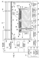
- FIG. 1 depicts a schematic diagram of one embodiment of an etch reactor 100 in which a method of quartz etching of the present invention may be practiced.
- Suitable reactors that may be adapted for use with the teachings disclosed herein include, for example, the Decoupled Plasma Source (DPS ® ) II reactor, or the TETRA TM I and TETRA TM II Photomask etch systems, all of which are available from Applied Materials, Inc. of Santa Clara, California.
- the DPS ® II reactor may also be used as a processing module of a CENTURA ® integrated semiconductor wafer processing system, also available from Applied Materials, Inc.
- the particular embodiment of the reactor 100 shown herein is provided for illustrative purposes and should not be used to limit the scope of the invention.
- the reactor 100 generally comprises a process chamber 102 having a substrate pedestal 124 within a conductive body (wall) 104, and a controller 146.
- the chamber 102 has a substantially flat dielectric ceiling 108. Other modifications of the chamber 102 may have other types of ceilings, e.g., a dome-shaped ceiling.
- An antenna 110 is disposed above the ceiling 108.
- the antenna 110 comprises one or more inductive coil elements that may be selectively controlled (two co-axial elements 110a and 110b are shown in Figure 1 ).
- the antenna 110 is coupled through a first matching network 114 to a plasma power source 112.
- the plasma power source 112 is typically capable of producing a radio frequency (RF) signal of up to about 3000 Watts (W) at a tunable frequency in a range from about 2 MHz to about 200 MHz, for example, 13.56 MHz. In one embodiment, the plasma power source 112 provides about 300 to about 600 W of inductively coupled RF power.
- RF radio frequency
- the substrate pedestal (cathode) 124 is coupled through a second matching network 142 to a biasing power source 140.
- the biasing source 140 provides an RF signal of between about zero to about 600 W at a tunable frequency in a range from about 2 MHz to about 200 MHz, for example, 13.56 MHz.
- the biasing source 140 may be configured to provide a continuous wave output or a pulsed output having a tunable pulse frequency in the range of from about 1 to about 10 kHz. Alternatively, the biasing source 140 may produce pulsed DC power output.
- the biasing source 140 is configured to provide RF power less than about 600 Watts at a frequency between about 1 to about 10 kHz, with a duty cycle between about 10 to about 95 percent. In another embodiment, the biasing source 140 is configured to provide RF power between about 20 to about 150 Watts, at a frequency between about 2 to about 5 kHz, with a duty cycle between about 80 to about 95 percent.
- the substrate support pedestal 124 may include an electrostatic chuck 160.
- the electrostatic chuck 160 comprises at least one clamping electrode 132 and is controlled by a chuck power supply 166.
- the substrate pedestal 124 may comprise substrate retention mechanisms such as a susceptor clamp ring, a mechanical chuck, and the like.
- a gas panel 120 is coupled to the process chamber 102 to provide process and/or other gases to the interior of the process chamber 102.
- the gas panel 120 is coupled to one or more inlets 116 formed in a channel 118 in the sidewall 104 of the chamber 102. It is contemplated that the one or more inlets 116 may be provided in other locations, for example, in the ceiling 108 of the process chamber 102.
- the gas panel 120 is adapted to selectively provide one or more process gases through the inlets 116 and into the interior of the process chamber 102 during processing.
- the gas panel 120 may be adapted to selectively provide a fluorine-containing and/or a chlorine-containing process gas (or gases) into the interior of the process chamber 102, as described below in connection with methods of etching a photomask.
- a plasma is formed from the gas and maintained through inductive coupling of power from the plasma power source 112.
- the plasma may alternatively be formed remotely or ignited by other methods.
- the pressure in the chamber 102 is controlled using a throttle valve 162 and a vacuum pump 164.
- the vacuum pump 164 and throttle valve 162 are capable of maintaining chamber pressures in the range of about 1 to about 20 mTorr.
- the temperature of the wall 104 may be controlled using liquid-containing conduits (not shown) that run through the wall 104. Wall temperature is generally maintained at about 65 degrees Celsius.
- the chamber wall 104 is formed from a metal (e.g., aluminum, stainless steel, and the like) and is coupled to an electrical ground 106.
- the process chamber 102 also comprises conventional systems for process control, internal diagnostic, end point detection, and the like. Such systems are collectively shown as support systems 154.
- a reticle adapter 182 is used to secure a substrate (such as a reticle or other workpiece) 122 onto the substrate support pedestal 124.
- the reticle adapter 182 generally includes a lower portion 184 milled to cover an upper surface of the pedestal 124 (for example, the electrostatic chuck 160) and a top portion 186 having an opening 188 that is sized and shaped to hold the substrate 122.
- the opening 188 is generally substantially centered with respect to the pedestal 124.
- the adapter 182 is generally formed from a single piece of etch resistant, high temperature resistant material such as polyimide ceramic or quartz.
- a suitable reticle adapter is disclosed in U.S. Patent No. 6,251,217 , issued on June 26, 2001, and incorporated herein by reference.
- An edge ring 126 may cover and/or secure the adapter 182 to the pedestal 124.
- a lift mechanism 138 is used to lower or raise the adapter 182, and hence, the substrate 122, onto or off of the substrate support pedestal 124.
- the lift mechanism 138 comprises a plurality of lift pins (one lift pin 130 is shown) that travel through respective guide holes 136.
- the temperature of the substrate 122 is controlled by stabilizing the temperature of the substrate pedestal 124.
- the substrate support pedestal 124 comprises a heater 144 and an optional heat sink 128.
- the heater 144 may be one or more fluid conduits configured to flow a heat transfer fluid therethrough.
- the heater 144 may include at least one heating element 134 that is regulated by a heater power supply 168.
- a backside gas e.g., helium (He)
- He helium
- the backside gas is used to facilitate heat transfer between the pedestal 124 and the substrate 122.
- the pedestal 124 may be heated by the embedded heater 144 to a steady-state temperature, which in combination with the helium backside gas, facilitates uniform heating of the substrate 122.
- the controller 146 comprises a central processing unit (CPU) 150, a memory 148, and support circuits 152 for the CPU 150 and facilitates control of the components of the process chamber 102 and, as such, of the etch process, as discussed below in further detail.
- the controller 146 may be one of any form of general-purpose computer processor that can be used in an industrial setting for controlling various chambers and sub-processors.
- the memory 148 of the CPU 150 may be one or more of readily available memory such as random access memory (RAM), read only memory (ROM), floppy disk, hard disk, or any other form of digital storage, local or remote.
- the support circuits 152 are coupled to the CPU 150 for supporting the processor in a conventional manner.
- circuits include cache, power supplies, clock circuits, input/output circuitry and subsystems, and the like.
- the inventive method is generally stored in the memory 148 or other computer-readable medium accessible to the CPU 150 as a software routine.
- software routine may also be stored and/or executed by a second CPU (not shown) that is remotely located from the hardware being controlled by the CPU 150.
- FIG 2 is a flow diagram of one embodiment of a method 200 for etching quartz. Although the method 200 is described below with reference to a substrate utilized to fabricate a photomask (as described above in Figure 1 ), the method 200 may also be used in other quartz etching applications.
- the method 200 begins at step 201 and proceeds to step 202.
- the substrate 122 is placed on a support pedestal 124 in a process chamber.
- the process chamber may be a TETRA TM I, TETRA TM II, DPS ® II, or other suitable etch chamber, as described above.
- the substrate 122 rests in the opening 188 of the adapter 182.
- the substrate 122 depicted in Figure 1 includes an optically transparent silicon based material, such as quartz (e.g., silicon dioxide, SiO 2 layer 192), having an opaque light-shielding layer of metal, known as a photomask material 190, forming a patterned mask on the surface of the quartz layer 192. It is contemplated that a separate mask may be utilized, or in other applications, a mask disposed on the quartz layer 192 may be comprised of different materials, and may include or be separated from the substrate by one or more intervening layers. Typical metals suitable for use as a photomask layer 190 include chromium and/or chromium oxynitride.
- the substrate 122 may also include a layer (not shown) of silicon nitride (SiN) doped with molybdenum (Mo) interposed between the quartz layer 192 and photomask layer 190.
- the quartz layer 192 of the substrate 122 is etched using a multi-step etch process.
- the multi-step etch process comprises a first etch step 206, wherein the substrate is etched using a first process gas comprising one or more fluorocarbon gases and a chlorine-containing gas, and a second etch step 208, wherein the substrate is etched using a second process gas comprising one or more fluorine-containing gases.
- Steps 206 and 208 may be performed in either order.
- one or more of steps 206 and 208 may be repeated as desired to continue the multi-step etch process until a desired endpoint is reached.
- a first process gas comprising one or more fluorocarbon gases and a chlorine-containing gas is introduced into the process chamber 102 through the gas inlet 116.
- the first process gas may further include an inert gas, such as helium (He), argon (Ar), xenon (Xe), neon (Ne), krypton (Kr), and the like.
- Exemplary chlorine-containing gases may include chlorine (Cl 2 ), hydrogen chloride (HCl), and the like.
- the chlorine-containing gas comprises chlorine (Cl 2 ).
- Cl 2 is provided at a rate of between about 1 - 10 standard cubic centimeters per minute (sccm). In one embodiment, Cl 2 at a rate of about 5 sccm is used.
- the pressure in the process chamber is controlled to less than about 40 mTorr, and in one embodiment, between about 1 and about 10 mTorr, for example 2 mTorr.
- Exemplary fluorocarbon gases may include CF 4 , CHF 3 , C 2 F, C 4 F 6 , C 4 F 8 , and the like.
- CF 4 is provided at a rate of between about 2 - 50 sccm and CHF 3 is provided at a rate of between about 2 - 50 sccm.
- CF 4 at a rate of about 9 sccm, and CHF 3 at a rate of about 26 sccm are used.
- the pressure in the process chamber is controlled to less than about 40 mTorr, and in one embodiment, between about 1 and about 10 mTorr, for example 2 mTorr.
- a substrate bias power is applied to the support pedestal 124 to bias the substrate 122.
- the bias power may be less than about 150 W, or in a first example, less than about 100 W, or in a second example, between 20 and about 150 W. In one embodiment, about 65 W of bias power is used for the process.
- the bias power may further be a 13.56 MHz RF signal provided at a continuous wave output or pulsed at a pulse frequency of between about 1 - 10 kHz, or in one embodiment, between about 2 - 5kHz.
- the bias power may be pulsed in a duty cycle of between about 10 - 95 percent, or in one embodiment, between about 20 - 95 percent.
- the biasing source 140 is configured to provide less than about 150 Watts of RF power at a pulse frequency between about 1 to about 10 kHz, with a duty cycle between about 10 to about 95 percent.
- the biasing source 140 is configured to provide between about 20 to about 150 Watts of RF power at a pulse frequency between about 2 to about 5 kHz, with a duty cycle between about 10 to about 95 percent.
- the biasing source 140 may provide a pulsed RF power between about 20 to about 150 Watts, at a pulse frequency between about 2 to about 5 kHz, with a duty cycle between about 10 to about 90 percent. In an embodiment wherein the quartz layer does not have a layer of patterned photoresist thereover, the biasing source 140 may provide a pulsed RF power between about 20 to about 150 Watts, at a pulse frequency between about 2 to about 5 kHz, with a duty cycle between about 10 to about 50 percent.
- Plasma is formed from the first process gas by applying RF power of between about 300 to about 600 W from the plasma power source 112 to the antenna 110. It is contemplated that the plasma may be ignited by other methods. In one embodiment, RF power of about 420 W is applied to the antenna 110 at a frequency of about 13.56 MHz.
- the quartz layer 192 exposed on the substrate 122 is etched for a first period of time until a desired endpoint for step 206 is reached. The endpoint may be determined by time, optical interferometry or by other suitable methods.
- a second process gas comprising one or more fluorocarbon gases are introduced into the process chamber 102 through the gas inlet 116.
- the second process gas may further include one or more inert gases, such as He, Ar, Xe, Ne, Kr, and the like.
- Exemplary fluorocarbon gases may include CF 4 , CHF 3 , C 2 F, C 4 F 6 , C 4 F 8 , and the like.
- CF 4 is provided at a rate of between about 2 - 50 sccm and CHF 3 is provided at a rate of between about 2 - 50 sccm.
- CF 4 at a rate of about 9 sccm, and CHF 3 at a rate of about 26 sccm are used.
- the pressure in the process chamber is controlled to less than about 40 mTorr, and in one embodiment, between about 1 and about 10 mTorr, for example 2 mTorr.
- a substrate bias power is applied to the support pedestal 124 to bias the substrate 122.
- the bias power may be less than about 150 W, or in a first example, less than about 100 W, or in a second example, between about 20 and about 150 W. In one embodiment, about 65 W of bias power is used for the process.
- the bias power may further be an RF signal provided at a continuous wave output or pulsed at a pulse frequency of between about 1 - 10 kHz, or in one embodiment, between about 2 - 5kHz.
- the bias power may be pulsed in a duty cycle of between about 10 - 95 percent, or in one embodiment, between about 20 - 95 percent.
- the biasing source 140 is configured to provide less than about 150 Watts of RF power at a pulse frequency between about 1 to about 10 kHz, with a duty cycle between about 10 to about 95 percent.
- the biasing source 140 is configured to provide between about 20 to about 150 Watts of RF power at a pulse frequency between about 2 to about 5 kHz, with a duty cycle between about 10 to about 95 percent.
- the biasing source 140 may provide a pulsed RF power between about 20 to about 150 Watts, at a pulse frequency between about 2 to about 5 kHz, with a duty cycle between about 10 to about 90 percent. In an embodiment wherein the quartz layer does not have a layer of patterned photoresist thereover, the biasing source 140 may provide a pulsed RF power between about 20 to about 150 Watts, at a pulse frequency between about 2 to about 5 kHz, with a duty cycle between about 10 to about 50 percent.
- Plasma is formed from the second process gas by applying RF power of between about 300 to about 600 W from the plasma power source 112 to the antenna 110. As discussed above at step 206, it is contemplated that the plasma may be ignited by other methods. In one embodiment, RF power of about 420 W is applied to the antenna 110 at a frequency of about 13.56 MHz. During step 208, the quartz layer 192 exposed on the substrate 122 is etched for a second period of time until a desired endpoint for step 208 is reached.
- step 210 it is queried whether a desired endpoint for the multi-step etch process is reached.
- the endpoint may be determined by time, optical interferometry, or by other suitable methods.
- the substrate may be removed from the chamber to facilitate ex-situ etch depth measurement and returned to the chamber for additional processing if necessary. If the answer to the query at step 210 is yes, the process ends at step 211 and the substrate may continue with any further processing as necessary. If the answer is no, the method returns to step 204. For further iterations of step 204, it is contemplated that the multi-step process may end after only repeating one of steps 206 or 208 upon reaching the desired multi-step etch endpoint.
- steps 206 and/or 208 repeated during iterations of step 204 may be different than from prior iterations (e.g., the duration of any step 206 or 208 during any iteration may be longer, shorter, or the same as any other duration of any step 206 or 208 from any prior iteration).
- the multi-step etching process as used in certain embodiments further provide uniformity control for the etched feature.
- the above etch process utilized in step 206 provides a center-fast etch (i.e., the central portion of the substrate is etched at a faster rate than peripheral portions of the substrate), while the etch process utilized in step 208 provides a center-slow etch (i.e., the central portion of the substrate is etched at a slower rate than peripheral portions of the substrate).
- the method 200 advantageously combines the two steps into a multi-step etch process having greater uniformity and phase angle range as compared to conventional methods.
- the method 200 further advantageously provides for reduced RIE lag, microtrenching, and more vertical sidewall angle control as compared to conventional etch methods.
- the method 200 is highly desirable in small critical dimension applications. It is to be appreciated, as discussed above, that the inventive method can begin with either of step 206 or step 208 and can be repeated in any sequence to provide further control as needed until the desired endpoint is reached.
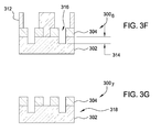
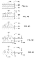
- Figures 3A-G depict one embodiment of a film stack 300 i fabricated into a quartz phase shift mask 318 utilizing the method 200 described above.
- the subscript "i" is an integer representing different fabrication stages the film stack shown in Figures 3A-G .
- the film stack 300 1 depicted in Figure 3A includes a quartz layer 302 having a photomask layer 304 disposed thereon.
- the photomask layer 304 is typically chromium or other suitable material such as those described above.
- An optional antireflection layer 306 (shown in phantom) may be disposed on the photomask layer 304.
- a first resist layer 308 is disposed on the photomask layer 304 or antireflection layer 306, when present.
- the first resist layer 308 is patterned and utilized as an etch mask to etch the photomask layer 304 to form features 310 exposing the underlying quartz layer 302 as depicted in Figure 3B .
- the photomask layer 304 may be etched using a plasma formed from chlorine-containing gas (such as Cl 2 ) mixed with oxygen.
- Cl 2 chlorine-containing gas
- One exemplary etch process is described in United States Patent Application Serial No. 10/235,223, filed September 4, 2002 , which is incorporated herein by reference in its entirety. It is contemplated that other suitable metal etch processes may be utilized.
- the remaining first resist layer 308 is removed, for example, by ashing, to leave the film stack 300 3 as shown in Figure 3C .
- a second resist layer 312 is disposed on the film stack 300 4 , filling the features 310.
- the second resist layer 312 is then patterned.
- the patterned second resist layer 312 exposes the quartz layer 302 at the bottom of alternating features 310, as shown in Figure 3E .
- the quartz layer 302 exposed through the patterned second resist layer 312 is etched using the method 200 described above (e.g., a multi-step etching process is used as previously described and, in one embodiment, to obtained controlled uniformity for the etched feature).
- the endpoint of the quartz etch is selected such that a depth 314 of the etched quartz trench 316 shown in Figure 3F is about equal to the length of 180 degrees phase shift through the quartz layer 302 for a predefined wavelength of light intended for use with the quartz phase shift mask 318. Typical wavelengths are 193 and 248 nm.
- the depth 314 is typically about either 172 or 240 nm, although other depths may be utilized for masks intended for use with different lithographic light wavelengths and/or manufacturing process flows.
- the remaining second resist layer 312 is removed, for example, by ashing, such that the remaining film stack 300 7 forms a quartz phase shift mask 318 as shown in Figure 3G .
- Figures 4A-E depict one embodiment of a film stack 400 i fabricated into a chromeless etch lithography mask 418 utilizing the method 300 described above.
- the subscript "i" is an integer representing different fabrication stages the film stack shown in Figures 4A-E .
- the film stack 400 1 depicted in Figure 4A includes a quartz layer 402 having a mask layer 404 disposed thereon.
- the mask layer 404 is generally suitable for selectively etching quartz using fluorinated plasma chemistries, and in one embodiment is chromium or other photomask material.
- An optional antireflection layer 406 (shown in phantom) may be disposed on the mask layer 404.
- a resist layer 408 is disposed on the mask layer 404 or antireflection layer 406, when present.
- the resist layer 408 is patterned and utilized as a etch mask to etch the mask layer 404 to form features 410 exposing the underlying quartz layer 402 as depicted in Figure 4B .
- the mask layer 404 may be etched using a plasma formed from chlorine-containing gases as described above.
- the remaining resist layer 408 is removed, for example, by ashing, to leave the film stack 400 3 shown in Figure 4C .
- the resist layer 408 may remain on the mask layer 404 and removed through erosion and/or stripping during subsequent processing.
- the quartz layer 402 exposed through the mask layer 404 at the bottom of the features 410 is etched using the method 200 described above (e.g., a multi-step etching process is used as previously described, and in one embodiment, to obtained controlled uniformity for the etched feature).
- the endpoint of the quartz etch is selected such that a depth 414 of the etched quartz trench 416 shown in Figure 4D is about equal to the length of 180 degrees phase shift through the quartz layer 402 for a predefined wavelength of light intended for use with the chromeless etch lithography mask 418, e.g., the depth 414 is selected as described with reference to the mask 318 above.
- the remaining portions of the mask layer 404 may optionally be removed.
- the remaining portions of the mask layer 404 may be removed by selectively etching, for example, using chemistries utilized to pattern the mask layer 404.
- the quartz layer 402 remaining from the film stack 400 5 forms a chromeless etch lithography mask 418 shown in Figure 4E .
- a method for etching quartz has been provided that advantageously improves trench attributes over conventional processes.
- the method disclosed herein provides for greater uniformity and phase angle range as compared to conventional methods as well as providing reduced RIE lag, reduced microtrenching, and more vertical sidewall angle control as compared to conventional etch methods.
- the method of etching quartz described herein advantageously facilitates fabrication of phase shifting photomasks suitable for patterning features having sub-5 ⁇ m critical dimensions.
Landscapes
- Physics & Mathematics (AREA)
- General Physics & Mathematics (AREA)
- Drying Of Semiconductors (AREA)
Applications Claiming Priority (1)
| Application Number | Priority Date | Filing Date | Title |
|---|---|---|---|
| US11/612,036 US7786019B2 (en) | 2006-12-18 | 2006-12-18 | Multi-step photomask etching with chlorine for uniformity control |
Publications (1)
| Publication Number | Publication Date |
|---|---|
| EP1947508A1 true EP1947508A1 (en) | 2008-07-23 |
Family
ID=39247304
Family Applications (1)
| Application Number | Title | Priority Date | Filing Date |
|---|---|---|---|
| EP07122837A Withdrawn EP1947508A1 (en) | 2006-12-18 | 2007-12-11 | Multi-step photomask etching with chlorine for uniformity control |
Country Status (5)
| Country | Link |
|---|---|
| US (1) | US7786019B2 (enExample) |
| EP (1) | EP1947508A1 (enExample) |
| JP (1) | JP2010514224A (enExample) |
| KR (1) | KR100988112B1 (enExample) |
| WO (1) | WO2008077012A2 (enExample) |
Families Citing this family (6)
| Publication number | Priority date | Publication date | Assignee | Title |
|---|---|---|---|---|
| US8956809B2 (en) * | 2012-08-03 | 2015-02-17 | Applied Materials, Inc. | Apparatus and methods for etching quartz substrate in photomask manufacturing applications |
| US9653316B2 (en) * | 2013-02-18 | 2017-05-16 | Tokyo Electron Limited | Plasma processing method and plasma processing apparatus |
| JP6267989B2 (ja) * | 2013-02-18 | 2018-01-24 | 東京エレクトロン株式会社 | プラズマ処理方法及び容量結合型プラズマ処理装置 |
| US20150371889A1 (en) * | 2014-06-20 | 2015-12-24 | Applied Materials, Inc. | Methods for shallow trench isolation formation in a silicon germanium layer |
| JP7333752B2 (ja) * | 2019-12-25 | 2023-08-25 | 東京エレクトロン株式会社 | 基板処理方法及び基板処理装置 |
| JP7434669B2 (ja) * | 2021-06-21 | 2024-02-20 | 東京エレクトロン株式会社 | プラズマ処理装置及びプラズマ処理方法 |
Citations (6)
| Publication number | Priority date | Publication date | Assignee | Title |
|---|---|---|---|---|
| JPH05144779A (ja) * | 1991-11-21 | 1993-06-11 | Matsushita Electric Ind Co Ltd | シリコン酸化膜のドライエツチング方法 |
| US5322590A (en) * | 1991-03-24 | 1994-06-21 | Tokyo Electron Limited | Plasma-process system with improved end-point detecting scheme |
| US5356515A (en) * | 1990-10-19 | 1994-10-18 | Tokyo Electron Limited | Dry etching method |
| US6251217B1 (en) | 1999-01-27 | 2001-06-26 | Applied Materials, Inc. | Reticle adapter for a reactive ion etch system |
| US20030049934A1 (en) | 2001-09-04 | 2003-03-13 | Applied Materials, Inc. | Methods and apparatus for etching metal layers on substrates |
| EP1686422A2 (en) * | 2005-01-27 | 2006-08-02 | Applied Materials, Inc. | Method for photomask plasma etching using a protected mask |
Family Cites Families (66)
| Publication number | Priority date | Publication date | Assignee | Title |
|---|---|---|---|---|
| US4263088A (en) * | 1979-06-25 | 1981-04-21 | Motorola, Inc. | Method for process control of a plasma reaction |
| US4357195A (en) * | 1979-06-25 | 1982-11-02 | Tegal Corporation | Apparatus for controlling a plasma reaction |
| JPS5947733A (ja) | 1982-09-13 | 1984-03-17 | Hitachi Ltd | プラズマプロセス方法および装置 |
| JPS6050923A (ja) | 1983-08-31 | 1985-03-22 | Hitachi Ltd | プラズマ表面処理方法 |
| JPS6062125A (ja) | 1983-09-16 | 1985-04-10 | Toshiba Corp | プラズマエツチング方法 |
| JPS611023A (ja) | 1984-06-13 | 1986-01-07 | Teru Saamuko Kk | バツチプラズマ装置 |
| US4855017A (en) * | 1985-05-03 | 1989-08-08 | Texas Instruments Incorporated | Trench etch process for a single-wafer RIE dry etch reactor |
| US4784720A (en) * | 1985-05-03 | 1988-11-15 | Texas Instruments Incorporated | Trench etch process for a single-wafer RIE dry etch reactor |
| CA1260365A (en) | 1985-05-06 | 1989-09-26 | Lee Chen | Anisotropic silicon etching in fluorinated plasma |
| JPS61263125A (ja) | 1985-05-15 | 1986-11-21 | Tokuda Seisakusho Ltd | ドライエツチング装置 |
| DE3613181C2 (de) | 1986-04-18 | 1995-09-07 | Siemens Ag | Verfahren zum Erzeugen von Gräben mit einstellbarer Steilheit der Grabenwände in aus Silizium bestehenden Halbleitersubstraten |
| JPS62253785A (ja) * | 1986-04-28 | 1987-11-05 | Tokyo Univ | 間欠的エツチング方法 |
| JPS6313334A (ja) | 1986-07-04 | 1988-01-20 | Hitachi Ltd | ドライエツチング方法 |
| JPH0691035B2 (ja) | 1986-11-04 | 1994-11-14 | 株式会社日立製作所 | 低温ドライエツチング方法及びその装置 |
| FR2616030A1 (fr) | 1987-06-01 | 1988-12-02 | Commissariat Energie Atomique | Procede de gravure ou de depot par plasma et dispositif pour la mise en oeuvre du procede |
| DE3733135C1 (de) * | 1987-10-01 | 1988-09-22 | Leybold Ag | Vorrichtung zum Beschichten oder AEtzen mittels eines Plasmas |
| GB2212974B (en) * | 1987-11-25 | 1992-02-12 | Fuji Electric Co Ltd | Plasma processing apparatus |
| JP2860653B2 (ja) | 1988-06-13 | 1999-02-24 | 東京エレクトロン株式会社 | プラズマ処理方法 |
| JPH02156529A (ja) | 1988-10-11 | 1990-06-15 | Tegal Corp | 半導体ウェーハの酸化物層傾斜エッチング方法 |
| JP2918892B2 (ja) | 1988-10-14 | 1999-07-12 | 株式会社日立製作所 | プラズマエッチング処理方法 |
| KR900013595A (ko) | 1989-02-15 | 1990-09-06 | 미다 가쓰시게 | 플라즈마 에칭방법 및 장치 |
| US4889588A (en) * | 1989-05-01 | 1989-12-26 | Tegal Corporation | Plasma etch isotropy control |
| JPH02312229A (ja) | 1989-05-26 | 1990-12-27 | Fuji Electric Co Ltd | プラズマエッチング方法 |
| JPH0383335A (ja) | 1989-08-28 | 1991-04-09 | Hitachi Ltd | エッチング方法 |
| JPH03129820A (ja) | 1989-10-16 | 1991-06-03 | Seiko Epson Corp | 半導体製造装置及び半導体装置の製造方法 |
| DE3940083A1 (de) | 1989-12-04 | 1991-06-13 | Siemens Ag | Verfahren zum anisotropen trockenaetzen von aluminium bzw. aluminiumlegierungen enthaltenden leiterbahnen in integrierten halbleiterschaltungen |
| US5160408A (en) * | 1990-04-27 | 1992-11-03 | Micron Technology, Inc. | Method of isotropically dry etching a polysilicon containing runner with pulsed power |
| KR930004713B1 (ko) * | 1990-06-18 | 1993-06-03 | 삼성전자 주식회사 | 변조방식을 이용한 플라즈마 발생장치 및 방법 |
| JPH04303929A (ja) | 1991-01-29 | 1992-10-27 | Micron Technol Inc | シリコン基板をトレンチ・エッチングするための方法 |
| JPH04311033A (ja) | 1991-02-20 | 1992-11-02 | Micron Technol Inc | 半導体デバイスのエッチング後処理方法 |
| JP2988122B2 (ja) * | 1992-05-14 | 1999-12-06 | 日本電気株式会社 | ドライエッチング装置および半導体装置の製造方法 |
| JPH06342769A (ja) | 1992-08-21 | 1994-12-13 | Nissin Electric Co Ltd | エッチング方法及び装置 |
| US5352324A (en) * | 1992-11-05 | 1994-10-04 | Hitachi, Ltd. | Etching method and etching apparatus therefor |
| JP3064769B2 (ja) * | 1992-11-21 | 2000-07-12 | アルバック成膜株式会社 | 位相シフトマスクおよびその製造方法ならびにその位相シフトマスクを用いた露光方法 |
| US5674647A (en) * | 1992-11-21 | 1997-10-07 | Ulvac Coating Corporation | Phase shift mask and manufacturing method thereof and exposure method using phase shift mask |
| JPH06181185A (ja) | 1992-12-14 | 1994-06-28 | Toshiba Corp | プラズマ表面処理装置 |
| JP3453435B2 (ja) * | 1993-10-08 | 2003-10-06 | 大日本印刷株式会社 | 位相シフトマスクおよびその製造方法 |
| JPH07142453A (ja) | 1993-11-16 | 1995-06-02 | Kokusai Electric Co Ltd | プラズマエッチング装置 |
| US5468341A (en) * | 1993-12-28 | 1995-11-21 | Nec Corporation | Plasma-etching method and apparatus therefor |
| US5952128A (en) * | 1995-08-15 | 1999-09-14 | Ulvac Coating Corporation | Phase-shifting photomask blank and method of manufacturing the same as well as phase-shifting photomask |
| JPH0892765A (ja) * | 1994-09-22 | 1996-04-09 | Tokyo Electron Ltd | エッチング方法 |
| JP3799073B2 (ja) | 1994-11-04 | 2006-07-19 | 株式会社日立製作所 | ドライエッチング方法 |
| US5683538A (en) * | 1994-12-23 | 1997-11-04 | International Business Machines Corporation | Control of etch selectivity |
| US5614060A (en) * | 1995-03-23 | 1997-03-25 | Applied Materials, Inc. | Process and apparatus for etching metal in integrated circuit structure with high selectivity to photoresist and good metal etch residue removal |
| JP3397933B2 (ja) * | 1995-03-24 | 2003-04-21 | アルバック成膜株式会社 | 位相シフトフォトマスクブランクス、位相シフトフォトマスク、及びそれらの製造方法。 |
| JPH1079372A (ja) | 1996-09-03 | 1998-03-24 | Matsushita Electric Ind Co Ltd | プラズマ処理方法及びプラズマ処理装置 |
| DE19736370C2 (de) * | 1997-08-21 | 2001-12-06 | Bosch Gmbh Robert | Verfahren zum anisotropen Ätzen von Silizium |
| US6635185B2 (en) * | 1997-12-31 | 2003-10-21 | Alliedsignal Inc. | Method of etching and cleaning using fluorinated carbonyl compounds |
| JP2000114246A (ja) * | 1998-08-07 | 2000-04-21 | Ulvac Seimaku Kk | ドライエッチング方法および装置、フォトマスクおよびその作製方法、ならびに半導体回路およびその製作方法 |
| JP2000098582A (ja) * | 1998-09-17 | 2000-04-07 | Ulvac Seimaku Kk | 位相シフトフォトマスクブランクス、位相シフトフォトマスク及びそれらの製造方法、並びに該ブランクスの製造装置 |
| KR100311234B1 (ko) * | 1999-01-18 | 2001-11-02 | 학교법인 인하학원 | 고품위 유도결합 플라즈마 리액터 |
| US6716758B1 (en) * | 1999-08-25 | 2004-04-06 | Micron Technology, Inc. | Aspect ratio controlled etch selectivity using time modulated DC bias voltage |
| US6193855B1 (en) * | 1999-10-19 | 2001-02-27 | Applied Materials, Inc. | Use of modulated inductive power and bias power to reduce overhang and improve bottom coverage |
| JP2001201842A (ja) * | 1999-11-09 | 2001-07-27 | Ulvac Seimaku Kk | 位相シフトフォトマスクブランクス及び位相シフトフォトマスク並びに半導体装置の製造方法 |
| US6605543B1 (en) * | 1999-12-30 | 2003-08-12 | Koninklijke Philips Electronics N.V. | Process to control etch profiles in dual-implanted silicon films |
| WO2001096955A2 (en) | 2000-06-15 | 2001-12-20 | Applied Materials, Inc. | A method and apparatus for etching metal layers on substrates |
| US6635566B1 (en) * | 2000-06-15 | 2003-10-21 | Cypress Semiconductor Corporation | Method of making metallization and contact structures in an integrated circuit |
| DE10309711A1 (de) * | 2001-09-14 | 2004-09-16 | Robert Bosch Gmbh | Verfahren zum Einätzen von Strukturen in einem Ätzkörper mit einem Plasma |
| JP4131813B2 (ja) * | 2002-10-24 | 2008-08-13 | 株式会社半導体エネルギー研究所 | プラズマエッチング方法及び半導体装置の作製方法 |
| US20040097077A1 (en) | 2002-11-15 | 2004-05-20 | Applied Materials, Inc. | Method and apparatus for etching a deep trench |
| US20040132311A1 (en) * | 2003-01-06 | 2004-07-08 | Applied Materials, Inc. | Method of etching high-K dielectric materials |
| US8257546B2 (en) * | 2003-04-11 | 2012-09-04 | Applied Materials, Inc. | Method and system for monitoring an etch process |
| US6875807B2 (en) * | 2003-05-28 | 2005-04-05 | Indspec Chemical Corporation | Silane-modified phenolic resins and applications thereof |
| US6969568B2 (en) * | 2004-01-28 | 2005-11-29 | Freescale Semiconductor, Inc. | Method for etching a quartz layer in a photoresistless semiconductor mask |
| US7879510B2 (en) * | 2005-01-08 | 2011-02-01 | Applied Materials, Inc. | Method for quartz photomask plasma etching |
| US7829243B2 (en) * | 2005-01-27 | 2010-11-09 | Applied Materials, Inc. | Method for plasma etching a chromium layer suitable for photomask fabrication |
-
2006
- 2006-12-18 US US11/612,036 patent/US7786019B2/en active Active
-
2007
- 2007-12-11 EP EP07122837A patent/EP1947508A1/en not_active Withdrawn
- 2007-12-14 KR KR1020070130986A patent/KR100988112B1/ko not_active Expired - Fee Related
- 2007-12-18 WO PCT/US2007/087878 patent/WO2008077012A2/en not_active Ceased
- 2007-12-18 JP JP2009543131A patent/JP2010514224A/ja active Pending
Patent Citations (6)
| Publication number | Priority date | Publication date | Assignee | Title |
|---|---|---|---|---|
| US5356515A (en) * | 1990-10-19 | 1994-10-18 | Tokyo Electron Limited | Dry etching method |
| US5322590A (en) * | 1991-03-24 | 1994-06-21 | Tokyo Electron Limited | Plasma-process system with improved end-point detecting scheme |
| JPH05144779A (ja) * | 1991-11-21 | 1993-06-11 | Matsushita Electric Ind Co Ltd | シリコン酸化膜のドライエツチング方法 |
| US6251217B1 (en) | 1999-01-27 | 2001-06-26 | Applied Materials, Inc. | Reticle adapter for a reactive ion etch system |
| US20030049934A1 (en) | 2001-09-04 | 2003-03-13 | Applied Materials, Inc. | Methods and apparatus for etching metal layers on substrates |
| EP1686422A2 (en) * | 2005-01-27 | 2006-08-02 | Applied Materials, Inc. | Method for photomask plasma etching using a protected mask |
Non-Patent Citations (1)
| Title |
|---|
| HYOUNG-DO KIM ET AL: "Application of a multi-step quartz etching method to strong PSMs", PROCEEDINGS OF THE SPIE - THE INTERNATIONAL SOCIETY FOR OPTICAL ENGINEERING SPIE-INT. SOC. OPT. ENG USA, vol. 4409, 2001, pages 118 - 124, XP002476133, ISSN: 0277-786X * |
Also Published As
| Publication number | Publication date |
|---|---|
| KR20080056652A (ko) | 2008-06-23 |
| US20080142476A1 (en) | 2008-06-19 |
| JP2010514224A (ja) | 2010-04-30 |
| WO2008077012A3 (en) | 2008-08-07 |
| US7786019B2 (en) | 2010-08-31 |
| KR100988112B1 (ko) | 2010-10-18 |
| WO2008077012A2 (en) | 2008-06-26 |
Similar Documents
| Publication | Publication Date | Title |
|---|---|---|
| US7829243B2 (en) | Method for plasma etching a chromium layer suitable for photomask fabrication | |
| US7718539B2 (en) | Method for photomask fabrication utilizing a carbon hard mask | |
| US8293430B2 (en) | Method for etching a molybdenum layer suitable for photomask fabrication | |
| KR101095694B1 (ko) | 석영 포토마스크 플라스마 식각을 위한 방법 | |
| JP2006215552A5 (enExample) | ||
| US10199224B2 (en) | Method for improving CD micro-loading in photomask plasma etching | |
| EP1901119A2 (en) | Photomask having self-masking layer and methods of etching same | |
| JP5459945B2 (ja) | 位相シフトフォトマスク及びその製造方法 | |
| US7790334B2 (en) | Method for photomask plasma etching using a protected mask | |
| EP1947508A1 (en) | Multi-step photomask etching with chlorine for uniformity control | |
| CN101054673B (zh) | 利用保护性罩幕的光罩等离子体蚀刻法 |
Legal Events
| Date | Code | Title | Description |
|---|---|---|---|
| PUAI | Public reference made under article 153(3) epc to a published international application that has entered the european phase |
Free format text: ORIGINAL CODE: 0009012 |
|
| AK | Designated contracting states |
Kind code of ref document: A1 Designated state(s): AT BE BG CH CY CZ DE DK EE ES FI FR GB GR HU IE IS IT LI LT LU LV MC MT NL PL PT RO SE SI SK TR |
|
| AX | Request for extension of the european patent |
Extension state: AL BA HR MK RS |
|
| 17P | Request for examination filed |
Effective date: 20090123 |
|
| AKX | Designation fees paid |
Designated state(s): AT BE BG CH CY CZ DE DK EE ES FI FR GB GR HU IE IS IT LI LT LU LV MC MT NL PL PT RO SE SI SK TR |
|
| 17Q | First examination report despatched |
Effective date: 20090317 |
|
| STAA | Information on the status of an ep patent application or granted ep patent |
Free format text: STATUS: THE APPLICATION IS DEEMED TO BE WITHDRAWN |
|
| 18D | Application deemed to be withdrawn |
Effective date: 20151105 |