EP1936734A1 - Radiofrequenzschaltmodul auf einem Mehrschichtsubstrat - Google Patents
Radiofrequenzschaltmodul auf einem Mehrschichtsubstrat Download PDFInfo
- Publication number
- EP1936734A1 EP1936734A1 EP08003716A EP08003716A EP1936734A1 EP 1936734 A1 EP1936734 A1 EP 1936734A1 EP 08003716 A EP08003716 A EP 08003716A EP 08003716 A EP08003716 A EP 08003716A EP 1936734 A1 EP1936734 A1 EP 1936734A1
- Authority
- EP
- European Patent Office
- Prior art keywords
- radio frequency
- circuit module
- conductor
- exposed
- axial line
- Prior art date
- Legal status (The legal status is an assumption and is not a legal conclusion. Google has not performed a legal analysis and makes no representation as to the accuracy of the status listed.)
- Withdrawn
Links
Images





Classifications
-
- H—ELECTRICITY
- H05—ELECTRIC TECHNIQUES NOT OTHERWISE PROVIDED FOR
- H05K—PRINTED CIRCUITS; CASINGS OR CONSTRUCTIONAL DETAILS OF ELECTRIC APPARATUS; MANUFACTURE OF ASSEMBLAGES OF ELECTRICAL COMPONENTS
- H05K9/00—Screening of apparatus or components against electric or magnetic fields
-
- H—ELECTRICITY
- H01—ELECTRIC ELEMENTS
- H01P—WAVEGUIDES; RESONATORS, LINES, OR OTHER DEVICES OF THE WAVEGUIDE TYPE
- H01P5/00—Coupling devices of the waveguide type
- H01P5/08—Coupling devices of the waveguide type for linking dissimilar lines or devices
- H01P5/085—Coaxial-line/strip-line transitions
-
- H—ELECTRICITY
- H05—ELECTRIC TECHNIQUES NOT OTHERWISE PROVIDED FOR
- H05K—PRINTED CIRCUITS; CASINGS OR CONSTRUCTIONAL DETAILS OF ELECTRIC APPARATUS; MANUFACTURE OF ASSEMBLAGES OF ELECTRICAL COMPONENTS
- H05K1/00—Printed circuits
- H05K1/02—Details
- H05K1/0213—Electrical arrangements not otherwise provided for
- H05K1/0216—Reduction of cross-talk, noise or electromagnetic interference
- H05K1/0218—Reduction of cross-talk, noise or electromagnetic interference by printed shielding conductors, ground planes or power plane
- H05K1/0219—Printed shielding conductors for shielding around or between signal conductors, e.g. coplanar or coaxial printed shielding conductors
-
- H—ELECTRICITY
- H05—ELECTRIC TECHNIQUES NOT OTHERWISE PROVIDED FOR
- H05K—PRINTED CIRCUITS; CASINGS OR CONSTRUCTIONAL DETAILS OF ELECTRIC APPARATUS; MANUFACTURE OF ASSEMBLAGES OF ELECTRICAL COMPONENTS
- H05K1/00—Printed circuits
- H05K1/18—Printed circuits structurally associated with non-printed electric components
- H05K1/182—Printed circuits structurally associated with non-printed electric components associated with components mounted in printed circuit boards [PCB], e.g. insert-mounted components [IMC]
- H05K1/183—Printed circuits structurally associated with non-printed electric components associated with components mounted in printed circuit boards [PCB], e.g. insert-mounted components [IMC] associated with components mounted in and supported by recessed areas of the PCBs
-
- H—ELECTRICITY
- H05—ELECTRIC TECHNIQUES NOT OTHERWISE PROVIDED FOR
- H05K—PRINTED CIRCUITS; CASINGS OR CONSTRUCTIONAL DETAILS OF ELECTRIC APPARATUS; MANUFACTURE OF ASSEMBLAGES OF ELECTRICAL COMPONENTS
- H05K2201/00—Indexing scheme relating to printed circuits covered by H05K1/00
- H05K2201/09—Shape and layout
- H05K2201/09209—Shape and layout details of conductors
- H05K2201/09654—Shape and layout details of conductors covering at least two types of conductors provided for in H05K2201/09218 - H05K2201/095
- H05K2201/09809—Coaxial layout
-
- H—ELECTRICITY
- H05—ELECTRIC TECHNIQUES NOT OTHERWISE PROVIDED FOR
- H05K—PRINTED CIRCUITS; CASINGS OR CONSTRUCTIONAL DETAILS OF ELECTRIC APPARATUS; MANUFACTURE OF ASSEMBLAGES OF ELECTRICAL COMPONENTS
- H05K2201/00—Indexing scheme relating to printed circuits covered by H05K1/00
- H05K2201/09—Shape and layout
- H05K2201/09818—Shape or layout details not covered by a single group of H05K2201/09009 - H05K2201/09809
- H05K2201/09845—Stepped hole, via, edge, bump or conductor
-
- H—ELECTRICITY
- H05—ELECTRIC TECHNIQUES NOT OTHERWISE PROVIDED FOR
- H05K—PRINTED CIRCUITS; CASINGS OR CONSTRUCTIONAL DETAILS OF ELECTRIC APPARATUS; MANUFACTURE OF ASSEMBLAGES OF ELECTRICAL COMPONENTS
- H05K2201/00—Indexing scheme relating to printed circuits covered by H05K1/00
- H05K2201/10—Details of components or other objects attached to or integrated in a printed circuit board
- H05K2201/10227—Other objects, e.g. metallic pieces
- H05K2201/10356—Cables
-
- H—ELECTRICITY
- H05—ELECTRIC TECHNIQUES NOT OTHERWISE PROVIDED FOR
- H05K—PRINTED CIRCUITS; CASINGS OR CONSTRUCTIONAL DETAILS OF ELECTRIC APPARATUS; MANUFACTURE OF ASSEMBLAGES OF ELECTRICAL COMPONENTS
- H05K3/00—Apparatus or processes for manufacturing printed circuits
- H05K3/30—Assembling printed circuits with electric components, e.g. with resistors
- H05K3/32—Assembling printed circuits with electric components, e.g. with resistors electrically connecting electric components or wires to printed circuits
- H05K3/34—Assembling printed circuits with electric components, e.g. with resistors electrically connecting electric components or wires to printed circuits by soldering
- H05K3/3405—Edge mounted components, e.g. terminals
-
- H—ELECTRICITY
- H05—ELECTRIC TECHNIQUES NOT OTHERWISE PROVIDED FOR
- H05K—PRINTED CIRCUITS; CASINGS OR CONSTRUCTIONAL DETAILS OF ELECTRIC APPARATUS; MANUFACTURE OF ASSEMBLAGES OF ELECTRICAL COMPONENTS
- H05K3/00—Apparatus or processes for manufacturing printed circuits
- H05K3/30—Assembling printed circuits with electric components, e.g. with resistors
- H05K3/32—Assembling printed circuits with electric components, e.g. with resistors electrically connecting electric components or wires to printed circuits
- H05K3/34—Assembling printed circuits with electric components, e.g. with resistors electrically connecting electric components or wires to printed circuits by soldering
- H05K3/341—Surface mounted components
-
- H—ELECTRICITY
- H05—ELECTRIC TECHNIQUES NOT OTHERWISE PROVIDED FOR
- H05K—PRINTED CIRCUITS; CASINGS OR CONSTRUCTIONAL DETAILS OF ELECTRIC APPARATUS; MANUFACTURE OF ASSEMBLAGES OF ELECTRICAL COMPONENTS
- H05K3/00—Apparatus or processes for manufacturing printed circuits
- H05K3/30—Assembling printed circuits with electric components, e.g. with resistors
- H05K3/32—Assembling printed circuits with electric components, e.g. with resistors electrically connecting electric components or wires to printed circuits
- H05K3/34—Assembling printed circuits with electric components, e.g. with resistors electrically connecting electric components or wires to printed circuits by soldering
- H05K3/341—Surface mounted components
- H05K3/3421—Leaded components
Definitions
- the present invention relates to a radio frequency circuit module, such as monolithic radio frequency integrated circuit module or a hybrid microwave integrated circuit module, formed by mounting circuit elements on a circuit substrate having dielectric layers for a module and a communication apparatus using the radio frequency circuit.
- a radio frequency circuit module such as monolithic radio frequency integrated circuit module or a hybrid microwave integrated circuit module
- radio frequency integrated circuit module having a multi-layer circuit substrate, on which circuit elements such as active elements including transistors and diodes and passive elements including resistors and inductors, and wiring for mutually connecting the circuit elements are mounted.
- circuit elements such as active elements including transistors and diodes and passive elements including resistors and inductors, and wiring for mutually connecting the circuit elements are mounted.
- a transmission path having a high shield property such as a coaxial line, is used between transmission and reception terminals in many cases.
- FIG. 16A is an oblique view conceptually showing the vicinities of transmission and reception terminals of a conventional radio frequency integrated circuit module.
- FIG. 16B is a sectional view of FIG. 16A in a coaxial line direction.
- FIG. 16B shows a radio frequency integrated circuit module having a multi-layer circuit substrate 2001 formed by interposing an inner conductor 2002 having circuit elements mounted thereon, between first and second grounds 2003 and 2004 to form a strip line 2005.
- the inner conductor 2002 is led to a pad 2007 through a via (through hole) 2006.
- the pad 2007 is a transmission and reception terminal having a fixed area provided on a top layer or a bottom layer.
- a central conductor 2009 of a coaxial line 2008 is fixed to the pad 2007 by adhering using solder 2010.
- the first and second grounds 2003 and 2004 are electrically connected through vias 2011.
- An outer conductor 2012 of the coaxial line 2008 is adhered and fixed to the first ground 2003 by solder 2013.
- Radio frequency signals can be inputted to and outputted from the radio frequency integrated circuit module of such construction in such a state that circuit elements are integrated therein.
- the central conductor of the coaxial line to be shielded around it is exposed at a portion connected to the pad. Therefore, the central conductor is susceptible to electromagnetic waves radiated from circuit elements and wiring mounted near the central conductor or external electromagnetic noise.
- the central conductor of the coaxial line is pulled from the outside and consequently a warp is caused in the multi-layer circuit substrate, or stress from a contained cabinet is applied to the coaxial line.
- solder peels from the pad or ground, or a metal pattern peels from the multi-layer circuit substrate, and resultant wire breaking or poor connection degrades the electric connection state.
- a problem of the present invention is to provide a radio frequency integrated circuit that is not susceptible to the influence of the electromagnetic waves and that is not degraded in electrical connection state, and a radio frequency integrated circuit module and a communication apparatus having the radio frequency integrated circuit mounted thereon.
- the present invention is a radio frequency circuit including circuit elements mounted on a multi-layer circuit substrate having a dielectric, characterized in that an exposed connection portion is provided by removing a part of the dielectric, and a conductor line connected to the circuit elements and a transmission path for transmitting a radio frequency signal from/to the conductor line are connected together in a bottom portion of the exposed connection portion so as to be rectilinear in a three dimensional way.
- the exposed connection portion is disposed in such a position as to be less susceptible to influence of electromagnetic waves from the circuit elements.
- a connection portion of the conductor line and the transmission path is covered by a conductor having such a hole as to be able to take out the transmission path.
- the conductor line is formed in a taper form toward the connection portion of the conductor line and the transmission path.
- ceramic or alumina can be used as the dielectric.
- the conductor line and the transmission path are connected together so as to be rectilinear in a three dimensional way by providing a step in the bottom portion of the exposed connection portion. Furthermore, a part of the bottom portion of the exposed connection portion is a surface of ground, and an outer conductor of the transmission path is electrically connected to the ground. Furthermore, characteristic impedance matching in the connection portion can also be accomplished by changing the distance between the conductor and the connection portion of the conductor line and the transmission path or by changing the thickness of a dielectric of the multi-layer circuit substrate disposed across the connection portion of the conductor line and the transmission path from the exposed connection portion.
- the present invention is a module including a radio frequency circuit, the radio frequency circuit including circuit elements mounted on a multi-layer circuit substrate having a dielectric, characterized in that in the radio frequency circuit, an exposed connection portion is provided by removing a part of the dielectric, and a conductor line connected to the circuit elements and a transmission path for transmitting a radio frequency signal to the conductor line are connected together in a bottom portion of the exposed connection portion so as to be rectilinear in a three dimensional way.
- a communication apparatus of the present invention is characterized in that the module is mounted on a radio frequency signal processor.
- a multi-layer circuit substrate is formed of at least three layers including first to Nth (N ⁇ 3) layers.
- Such a strip line that an inner conductor disposed in some inner layer is interposed between first and second grounds has an exposed connection portion in its end portion.
- the exposed connection portion is formed by removing a dielectric layer or a metal layer on an upper side or a lower side of the inner conductor.
- a central conductor of a coaxial line serving as a transmission path is connected to the inner conductor exposed in the bottom portion of the exposed connection portion so as to be rectilinear.
- the characteristic impedance of the strip line is made equal to that of the coaxial line.
- the transmission characteristic of the connection portion between the inner conductor in the multi-layer circuit substrate and the coaxial line can be improved, and highly reliable signal transmission with a reduced reflection loss and radiation loss can be conducted. Furthermore, the shield performance in the connection portion between the inner conductor and the coaxial line can be improved. It is possible to suppress the interference of electromagnetic noise in the surroundings and conduct highly reliable signal transmission without radiating unnecessary electromagnetic waves to the surroundings.
- connection portion between the inner conductor in the multi-layer circuit substrate and the coaxial line can be enhanced. It is possible to prevent wire breaking or poor connection caused by deformation of the connection portion or signal degradation caused thereby. Highly reliable signal transmission can be conducted.
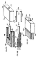
- FIG. 1A is an oblique view conceptually showing a radio frequency integrated circuit module of a first embodiment according to the present invention.
- FIG. 1B is a sectional view of FIG. 1A in a coaxial line direction.
- FIG. 1B shows a radio frequency integrated circuit module having a multi-layer circuit substrate 101 with a double layer structure formed by interposing an inner conductor 102 serving as a conductor line between first ground 103 and second ground 104 which form a strip line 105.
- a cavity shaped exposed connection portion 106 is provided on the first ground 103 side of the multi-layer circuit substrate 101.
- the dielectric layer or the metal layer is not provided, but an exposed portion of a central conductor 108 of a semi-rigid coaxial line (hereafter referred to as "coaxial line") 107 is fixed in such a manner that the coaxial line 107 is not affected by electromagnetic waves generated from circuit elements mounted around it.
- a square exposed connection portion 106 is formed.
- the exposed connection portion 106 may be a circle.
- the shape is not restricted to a square.
- the exposed connection portion 106 can be formed by etching or mechanical cutting.
- the exposed connection portion 106 is provided in such a position that the exposed portion of the central conductor 108 of the coaxial line 107 is not affected by electromagnetic waves generated from circuit elements mounted around it. Adhering and fixing is conducted by using solder 110 so that the exposed central conductor 108 and the exposed portion 109 of the inner conductor 102 may become nearly rectilinear.
- first ground 103 and the second ground 104 are electrically connected by vias 111 provided at near end portions of the strip line 105.
- an outer conductor 112 is fixed to the first ground 103 by solder 113.
- the solders 110 and 113 may include lead or may not include lead.
- the dielectric ceramic or alumina can be used.
- ceramic is used.
- the dielectric constant of the dielectric is set equal to, for example, 7.1.
- the thickness of the dielectric is set equal to, for example, 0.12 mm in each of the first and second grounds.
- the width and thickness of the inner conductor 102 are set equal to 0.05 mm and 0.01 mm, respectively.
- the characteristic impedance of the exposed connection portion 106 is set equal to approximately 50 ⁇ which is the characteristic impedance of the strip line 105 and the coaxial line 107.
- the fabrication precision can be raised as compared with the multi-layer circuit substrate made of FR4 that is generally widespread, and reliability of the transmission characteristics can be improved especially in a GHz band.
- the exposed portion 109 is made large enough to adhere the central conductor 108 of the coaxial line 107 serving as the transmission path to the exposed portion 109 by using the solder 110.
- FIG. 11 is a top view conceptually showing a portion of the inner conductor 102 in the vicinity of the exposed connection portion. This is because an impedance matching in the radio frequency band is in general difficult in a line rapidly changing in conductor width and resultant unnecessary reflection might degrade the radio frequency reflection characteristics.
- the width of the inner conductor 102 when, for example, the width of the inner conductor 102 is approximately 0.1 mm, the width is gradually widened from a position located at a distance of approximately 1.5 mm from the exposed portion 109 and the width is made approximately 0.5 mm in the exposed portion 109.
- the width of the inner conductor 102 is wider than that of the exposed portion 109, the width of the inner conductor 102 should be gradually narrowed from a position located at a distance of approximately 1.5 mm from the exposed portion 109 to form a tapered shape.
- the exposed connection portion 106 is provided and circuit elements are not formed near the central conductor 108 of the coaxial line 107.
- the exposed portion of the central conductor 108 is made less susceptible to the influence of electromagnetic waves.
- the solder 110 is provided within the exposed connection portion 106, the solder 110 is prevented from peeling off due to external force.
- the central conductor 108 of the coaxial line 107 is fixed to the inner conductor 102 so as to be rectilinear, the central conductor 108 can be electrically connected to the end portion of the inner conductor 102. Furthermore, since the inner conductor 102 is directly connected to the central conductor 108 of the coaxial line 107, a radio frequency integrated circuit module can be formed without hampering the impedance matching.
- the outer conductor 112 is adhered to the first ground 103 in three places by solder 113. Therefore, they can be connected together directly and firmly.
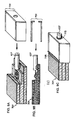
- FIG. 2A is an oblique view conceptually showing a radio frequency integrated circuit module of a second embodiment according to the present invention.
- FIG. 2B is a sectional view of FIG. 2A in a coaxial line direction.
- numeral 204 denotes an exposed connection portion provided in order to structurally make it hard to burden a load on the coaxial line 107.
- FIG. 2A the same components as those shown in FIG. 1A are denoted by like characters.
- a step between an exposed connection portion 106 and an exposed connection portion 204 is set equal to the radius of an outer conductor 112.
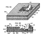
- FIG. 3A is an oblique view conceptually showing a radio frequency integrated circuit module of a third embodiment according to the present invention.
- FIG. 3B is a sectional view of FIG. 3A in a coaxial line direction.
- a multi-layer circuit substrate 301 of a five layer structure is used.
- numerals 307, 308 and 311 denote third to fifth grounds.
- Numerals 309 denote vias provided at a high density in a two dimensional way to connect the first and third grounds together and connect the second and fourth grounds together.
- Numeral 317 denotes solder for connecting an outer conductor 112 to the fifth ground 311.
- FIG. 3A the same portions as those shown in FIG. 2A are denoted by like characters.
- the present embodiment has been described by taking the case where the fifth ground 311 is provided, as an example.
- the outer conductor 112 and the second ground 104 may be directly connected together by solder 317.
- the multi-layer circuit substrate 301 of, for example, the five layer structure is used as in the present embodiment, degradation of the electric connection state can be prevented in the same way as the second embodiment. Reliability of the microwave transmission characteristics is also improved.
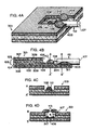
- FIG. 4A is an oblique view conceptually showing a radio frequency integrated circuit module of a forth embodiment according to the present invention.
- FIG. 4B is a sectional view of FIG. 4A in a coaxial line direction.
- FIG. 4C is a sectional view of FIG. 4B in an A-A' plane.
- FIG. 4D is a sectional view of FIG. 4B ) in a B-B' plane.
- numeral 403 denotes an end portion of the multi-layer circuit substrate 301.
- the same portions as those shown in FIG. 3A are denoted by like characters.
- side faces of the exposed connection portion 204 are provided on the end portion 403 of the multi-layer circuit substrate 301.
- a central conductor 108 of a coaxial line 107 is connected to an exposed portion 109 of an inner conductor 102.
- the coaxial line 107 is not bent.
- the load applied to solder 113 can be further reduced.
- the exposed connection portion 106 may be formed in the end portion of the radio frequency integrated circuit module.
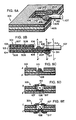
- FIG. 5A is an oblique view conceptually showing a radio frequency integrated circuit module of a fifth embodiment according to the present invention.
- FIG. 5B is a sectional view of FIG. 5A in a coaxial line direction.
- FIG. 5C is a sectional view of FIG. 5B in an A-A' plane.
- FIG. 5d is a sectional view of FIG. 5B in a B-B' plane.
- FIG. 5E is a sectional view of FIG. 5B in a C-C' plane.
- numeral 505 denotes a notch of an end portion 403.
- the same portions as those shown in FIG. 4A are denoted by like characters.
- firmer mechanical connection can be accomplished.
- FIG. 6A is an oblique view conceptually showing a radio frequency integrated circuit module of a sixth embodiment according to the present invention.
- FIG. 6B is a sectional view of FIG. 6A in a coaxial line direction.
- the width W of the multi-layer circuit substrate 301 is made equal to the width of the exposed connection portions 106 and 204.
- the same portions as those shown in FIG. 5A are denoted by like characters.
- the width W is set equal to approximately 2 mm.
- the exposed connection portions 106 and 204 of the radio frequency integrated circuit module as shown in FIG. 6A are formed by mechanical cutting, forming is easier than the exposed connection portion 106 shown in FIGS. 1A to 5E .
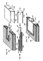
- FIG. 7A is an oblique view of the radio frequency integrated circuit module shown in FIG. 5A and a metal case made of, for example, copper that is a conductor case for covering the vicinities of transmission and reception terminals of the radio frequency integrated circuit module.
- FIG. 7B is a sectional view of FIG. 7A in a coaxial line direction.
- FIG. 7C is an illustrative view showing such a situation that a metal case 701 in the state of FIG. 7A is attached to the radio frequency integrated circuit module and they are adhered and fixed to each other by soldering.
- the metal case 701 includes two parallel flat metal plates 702 and a flat metal plate 709 having a hole 711 for passing a coaxial line 107.
- the interval between the two parallel flat metal plates 702 is set nearly equal to the thickness of the multi-layer circuit substrate 301.
- the width of the flat metal plate 702 is made larger than the width of the exposed connection portions 106 and 204.
- Conductive resin such as conductive plastic or resin having metal plating on the surface thereof may be used as the case 701.
- the coaxial line 107 is passed through the hole 711 and then the metal case 701 is attached to the radio frequency integrated circuit module.
- Third and fourth grounds 307 and 308 and the flat metal plates 702 are adhered and fixed to each other by solder 708.
- the coaxial line 107 and the hole 711 are adhered and fixed to each other by solder 713.
- the coaxial line 107 is fixed to the metal case 701.
- a tension force is applied from the outside to a cabinet containing the radio frequency integrated circuit module, the force is not applied directly to the solder 110 and 113. Accordingly, the solder 110 and 113 and the metal pattern are not easily peeled off.
- the metal case 701 electromagnetically shields the inner conductor 102 and the central conductor 108 of the coaxial line 107. It thus becomes possible to make a radio frequency signal less susceptible to external electromagnetic noise and make the radio frequency signal generate less electromagnetic noise to the outside. In addition, fine metallic powders are prevented from contacting with the exposed central conductor 108 of the coaxial line 107.
- the metal case 701 is U-shaped. As shown in FIG. 8A , however, the metal case 701 may be of box shape. Furthermore, it is also possible to use, for example, the radio frequency integrated circuit module shown in FIG. 6A and combine it with the metal case 701 taking the shape of box shape as shown in FIG. 9A . By the way, the metal case 701 shown in FIG. 7A is suitable, when the width of the radio frequency integrated circuit module is long.
- the metal case 701 as shown in FIGS. 8A and 9A can surround the exposed portion 109 and the central conductor 108 of the coaxial line 107 on all sides. As compared with the case where the metal case 701 shown in FIG. 7A is used, therefore, it becomes possible to make the module less susceptible to external electromagnetic noise and make the module hardly transmit electromagnetic noise to the outside.
- Each of the radio frequency integrated circuit modules shown in FIGS. 1A to 6B may have such a configuration as to be covered by the metal case 701.
- FIG. 10 is an oblique view showing such a state that the top of the exposed connection portion 106 of the radio frequency integrated circuit module shown in FIG. 3A is covered by a flat metal plate 901.
- the flat metal plate 901 includes a hole 905 having a diameter that is nearly equal to the outer diameter of the coaxial line 107.
- the coaxial line 107 is passed through the hole 905.
- the flat metal plate 901 and the coaxial line 107 are adhered and fixed to each other by solder 904.
- the flat metal plate 901 and the radio frequency integrated circuit module are adhered and fixed to each other by solder 907.
- the module can be made less susceptible to external electromagnetic noise.
- Each of the radio frequency integrated circuit modules shown in FIGS. 1A to 6B may have such a configuration as to be covered by the flat metal plate 901.
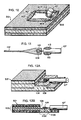
- FIG. 12A is an oblique view conceptually showing a radio frequency integrated circuit module of a ninth embodiment according to the present invention.
- FIG. 12B is a sectional view of FIG. 12A in a coaxial line direction.
- the characteristic impedance of the strip line 105 can be adjusted by changing the dielectric constant and thickness of the dielectric and the width and thickness of the inner conductor 102.
- the thickness and so on of the dielectric cannot be changed in some cases.
- the width of the inner conductor 102 and the thickness of the dielectric that is in contact with the inner conductor, in the section 1102 are altered.
- the characteristic impedance of the strip line 105 and the coaxial line 107 can be matched and impedance matching in the design stage is facilitated, in the present embodiment. Furthermore, the distributed parameter design of each ground is also facilitated. As a result, unnecessary reflection and radiation can be suppressed, and reliability of the transmission characteristics can be improved.
- FIG. 13A is an oblique view of the radio frequency integrated circuit module shown in FIG. 6A and a metal case made of, for example, copper that covers the vicinities of transmission and reception terminals of the radio frequency integrated circuit module.
- FIG. 13B is a sectional view of FIG. 13A in a coaxial line direction.
- FIG. 13C is a diagram showing such a situation that a metal case 1201 is attached to the radio frequency integrated circuit module in the state of FIG. 13A and they are adhered and fixed to each other by solder.
- the shape of the metal case 1201 is made different from that of the metal case 701 shown in, for example, FIG. 7A .
- This aims at making possible matching the characteristic impedance of the strip line 105 and the coaxial line 107 by adjusting the distance between the flat metal plate 1216 and the strip line 105 and the coaxial line 107, even when the thickness and so on of the dielectric cannot be changed, in the same way as the ninth embodiment.
- the transmission mode in such a section that the exposed connection portion 106 exists therein is considered to be a pseudo TEM (transverse electromagnetic) mode.
- the characteristic impedance is changed by the following parameters.
- the characteristic impedance is changed by changing any of the width of the exposed portion 109, the thickness of the dielectric, and the distance between the exposed portion 109 and the metal case 701. How to derive the characteristic impedance obtained when those parameters are changed will be described hereafter.
- FIG. 14 is a sectional view in the section where the exposed connection portion 106 exists.
- w is the width of the exposed portion 109
- h is the thickness of the dielectric
- s is the distance between the exposed section 109 and the metal case 1201.
- FIG. 15A is a graph showing normalized characteristic impedance Z 0 as a function of the width w of the exposed portion 109/ the thickness h of the dielectric.
- FIG. 15B is a graph showing normalized characteristic impedance Zo as a function of the distance s between the exposed portion 109 and the metal case 1201/ the thickness h of the dielectric.
- the characteristic impedance can be matched as shown in FIG. 15A and FIG. 15B by changing any of the three parameters w, h and s shown in FIG. 14 . Furthermore, as shown in FIG. 15A , the characteristic impedance Zo becomes 1 when, for example, w/h ⁇ 0.6. As shown in FIG. 15B , the characteristic impedance Zo becomes 1 when, for example, s/h ⁇ 0.9.
- the normalized characteristic impedance Zo has been obtained by normalizing with a certain value. Since the basic mode of the transmission line having a section as shown in FIG. 14 is considered to be the pseudo TEM mode, the static electromagnetic field in the section can be easily derived by analyzing with a commercially available electromagnetic simulator or the like.
- the second ground 104 is removed and the width of the inner conductor 102 in the section 1102 and the thickness of the dielectric that is in contact with the inner conductor are changed, in the same way as the ninth embodiment.
- the characteristic impedance in such a section 1102 that the exposed connection portion 106 exists therein is made equal to the characteristic impedance of the strip line 105 and the coaxial line 107.
- a communication apparatus such as a portable telephone or an optical communication apparatus includes a radio frequency signal processor for modulating a speech signal or an optical signal to a radio frequency signal and transmitting the radio frequency signal to another communication apparatus. If the radio frequency integrated circuit module described in each of the embodiments is mounted on the radio frequency signal processor of the communication apparatus, it becomes possible to provide a communication apparatus that is less susceptible to the influence of electromagnetic waves and that is not degraded in electric connection state.
Landscapes
- Engineering & Computer Science (AREA)
- Microelectronics & Electronic Packaging (AREA)
- Physics & Mathematics (AREA)
- Electromagnetism (AREA)
- Shielding Devices Or Components To Electric Or Magnetic Fields (AREA)
Applications Claiming Priority (2)
| Application Number | Priority Date | Filing Date | Title |
|---|---|---|---|
| JP2000136216A JP3976473B2 (ja) | 2000-05-09 | 2000-05-09 | 高周波回路及びそれを用いたモジュール、通信機 |
| EP01110761A EP1154512A3 (de) | 2000-05-09 | 2001-05-03 | Modul mit einer Hochfrequenzschaltung auf einem Mehrschichtsubstrat |
Related Parent Applications (1)
| Application Number | Title | Priority Date | Filing Date |
|---|---|---|---|
| EP01110761A Division EP1154512A3 (de) | 2000-05-09 | 2001-05-03 | Modul mit einer Hochfrequenzschaltung auf einem Mehrschichtsubstrat |
Publications (1)
| Publication Number | Publication Date |
|---|---|
| EP1936734A1 true EP1936734A1 (de) | 2008-06-25 |
Family
ID=18644195
Family Applications (2)
| Application Number | Title | Priority Date | Filing Date |
|---|---|---|---|
| EP01110761A Ceased EP1154512A3 (de) | 2000-05-09 | 2001-05-03 | Modul mit einer Hochfrequenzschaltung auf einem Mehrschichtsubstrat |
| EP08003716A Withdrawn EP1936734A1 (de) | 2000-05-09 | 2001-05-03 | Radiofrequenzschaltmodul auf einem Mehrschichtsubstrat |
Family Applications Before (1)
| Application Number | Title | Priority Date | Filing Date |
|---|---|---|---|
| EP01110761A Ceased EP1154512A3 (de) | 2000-05-09 | 2001-05-03 | Modul mit einer Hochfrequenzschaltung auf einem Mehrschichtsubstrat |
Country Status (4)
| Country | Link |
|---|---|
| US (3) | US6661318B2 (de) |
| EP (2) | EP1154512A3 (de) |
| JP (1) | JP3976473B2 (de) |
| KR (1) | KR100430299B1 (de) |
Cited By (1)
| Publication number | Priority date | Publication date | Assignee | Title |
|---|---|---|---|---|
| EP3080864A4 (de) * | 2013-12-09 | 2017-07-26 | Alcatel- Lucent Shanghai Bell Co., Ltd | Steckverbinder zur verbindung eines koaxialkabels mit einer streifenleitung |
Families Citing this family (53)
| Publication number | Priority date | Publication date | Assignee | Title |
|---|---|---|---|---|
| JP3998996B2 (ja) | 2002-03-01 | 2007-10-31 | 凌和電子株式会社 | 高周波伝送線路接続システムおよびその方法 |
| US6857898B2 (en) * | 2002-07-25 | 2005-02-22 | Tektronix, Inc. | Apparatus and method for low-profile mounting of a multi-conductor coaxial cable launch to an electronic circuit board |
| JP4219634B2 (ja) * | 2002-08-01 | 2009-02-04 | 凌和電子株式会社 | 磁気センサ、側面開放型temセル、およびこれらを利用した装置 |
| US6927655B2 (en) * | 2002-08-23 | 2005-08-09 | Opnext Japan, Inc. | Optical transmission module |
| JP4125570B2 (ja) | 2002-09-19 | 2008-07-30 | 日本電気株式会社 | 電子装置 |
| US7042318B2 (en) * | 2002-10-10 | 2006-05-09 | Agilent Technologies, Inc. | Shielded surface-mount coaxial edge launch connector |
| DE20217338U1 (de) * | 2002-11-06 | 2003-02-06 | Siemens AG, 80333 München | Leiterplatte mit einer Kontaktfläche für einen Antennenanschluss |
| US7180009B2 (en) * | 2004-07-30 | 2007-02-20 | Bae Systems Information And Electronic Systems Inteegration Inc. | Transmission line with stripped semi-rigid cable |
| DE102004060416B4 (de) * | 2004-12-14 | 2007-06-14 | Endress + Hauser Flowtec Ag | Verfahren zur Befestigung eines Koaxialkabels an einer Leiterplatte und entsprechende Leiterplatte |
| JP4873958B2 (ja) * | 2005-02-24 | 2012-02-08 | 京セラ株式会社 | 高周波デバイス実装基板 |
| TWI290443B (en) * | 2005-05-10 | 2007-11-21 | Via Tech Inc | Signal transmission structure, wire board and connector assembly structure |
| US9713258B2 (en) | 2006-04-27 | 2017-07-18 | International Business Machines Corporation | Integrated circuit chip packaging |
| US7557431B2 (en) * | 2007-01-18 | 2009-07-07 | Miteq, Inc. | Microwave surface mount hermetically sealed package and method of forming the same |
| JP5370883B2 (ja) * | 2008-05-30 | 2013-12-18 | 京セラSlcテクノロジー株式会社 | 配線基板 |
| JP5482663B2 (ja) * | 2008-11-26 | 2014-05-07 | 日本電気株式会社 | 回路モジュールの基板及びその製造方法 |
| FR2942569B1 (fr) * | 2009-02-25 | 2011-03-25 | Alcatel Lucent | Dispositif de connexion pour un cable coaxial transportant un signal haute frequence. |
| US8248183B2 (en) * | 2009-07-30 | 2012-08-21 | Sierra Wireless, Inc. | Circuit board pad having impedance matched to a transmission line and method for providing same |
| US8350638B2 (en) * | 2009-11-20 | 2013-01-08 | General Motors Llc | Connector assembly for providing capacitive coupling between a body and a coplanar waveguide and method of assembling |
| JP5420389B2 (ja) * | 2009-12-24 | 2014-02-19 | オリンパス株式会社 | ケーブル接続構造 |
| JP5631618B2 (ja) | 2010-04-08 | 2014-11-26 | オリンパス株式会社 | ケーブル接続構造 |
| JP5501846B2 (ja) * | 2010-05-07 | 2014-05-28 | オリンパス株式会社 | 電子デバイス、ケーブル接続構造および電子デバイスの製造方法 |
| JP2012064338A (ja) * | 2010-09-14 | 2012-03-29 | Fujitsu Ltd | 同軸ケーブルの端末構造、コネクタ及び基板ユニット |
| US9077072B2 (en) | 2010-09-20 | 2015-07-07 | General Motors Llc | Antenna system and filter |
| US8686906B2 (en) | 2010-09-20 | 2014-04-01 | GM Global Technology Operations LLC | Microwave antenna assemblies |
| US8704719B2 (en) | 2010-11-23 | 2014-04-22 | General Motors Llc | Multi-function antenna |
| CN103906348B (zh) * | 2010-12-03 | 2017-11-24 | 株式会社村田制作所 | 电子设备 |
| CN201966402U (zh) * | 2010-12-08 | 2011-09-07 | 富士康(昆山)电脑接插件有限公司 | 线缆连接器 |
| US20140206230A1 (en) * | 2013-01-18 | 2014-07-24 | Molex Incorporated | Paddle Card Assembly For High Speed Applications |
| US9466925B2 (en) | 2013-01-18 | 2016-10-11 | Molex, Llc | Paddle card assembly for high speed applications |
| US9049787B2 (en) | 2013-01-18 | 2015-06-02 | Molex Incorporated | Paddle card with improved performance |
| WO2014199897A1 (ja) * | 2013-06-10 | 2014-12-18 | オリンパス株式会社 | ケーブル接続構造 |
| CN205584615U (zh) * | 2013-12-12 | 2016-09-14 | 株式会社村田制作所 | 信号传输元器件及电子设备 |
| US10168425B2 (en) | 2014-07-03 | 2019-01-01 | GM Global Technology Operations LLC | Centralized vehicle radar methods and systems |
| WO2016063603A1 (ja) * | 2014-10-20 | 2016-04-28 | オリンパス株式会社 | 固体撮像装置およびこの固体撮像装置を備えた電子内視鏡 |
| US9373915B1 (en) | 2015-03-04 | 2016-06-21 | Molex, Llc | Ground shield for circuit board terminations |
| JP2016181349A (ja) * | 2015-03-23 | 2016-10-13 | 第一精工株式会社 | コネクタ装置及びその組立方法 |
| US20160329130A1 (en) * | 2015-05-07 | 2016-11-10 | Wilson Electronics, Llc | Flat coaxial cable |
| US9728912B2 (en) * | 2015-12-08 | 2017-08-08 | Intel Corporation | Micro-coax cable adaptor board |
| EP3249741B1 (de) * | 2016-05-24 | 2020-02-26 | Nokia Shanghai Bell Co., Ltd. | Vorrichtung zur verbindung zwischen einer streifenleitung und einem koaxialkabel |
| US10085337B2 (en) * | 2016-05-26 | 2018-09-25 | Institut National D'optique | Coaxial cable assembly, electronic package and connector |
| WO2018007580A1 (de) * | 2016-07-08 | 2018-01-11 | Hirschmann Car Communication Gmbh | Kabelmontage für koaxialkabel auf dicken leiterplatten |
| US10340233B1 (en) * | 2016-12-06 | 2019-07-02 | Lockheed Martin Corporation | Millimeter wave connectors to integrated circuit interposer boards |
| US9974160B1 (en) * | 2016-12-28 | 2018-05-15 | Raytheon Company | Interconnection system for a multilayered radio frequency circuit and method of fabrication |
| US20180191061A1 (en) * | 2017-01-05 | 2018-07-05 | Intel Corporation | Process technology for embedded horn structures with printed circuit boards |
| LT3435482T (lt) | 2017-07-25 | 2019-08-26 | Md Elektronik Gmbh | Prijungimo jungtis su kabelių sąranka ir plokščių sąranka, šios jungties gamybos būdas |
| CN107959107A (zh) * | 2017-10-27 | 2018-04-24 | 中国船舶重工集团公司第七二三研究所 | 一种基于厚薄带状线转换的同轴馈电毫米波天线 |
| JP6711860B2 (ja) * | 2018-04-18 | 2020-06-17 | 日本電信電話株式会社 | 高周波線路接続構造 |
| KR102022669B1 (ko) | 2019-06-21 | 2019-09-18 | 박민규 | 안구 보습기 |
| US12068520B2 (en) * | 2019-07-03 | 2024-08-20 | Kabushiki Kaisha Toshiba | Coaxial microstrip line conversion circuit |
| CN113839687B (zh) * | 2020-06-23 | 2025-06-13 | 户外无线网络有限公司 | 信号处理设备和天线系统 |
| CN112072435B (zh) * | 2020-08-14 | 2022-04-01 | 中国电子科技集团公司第十三研究所 | 射频电缆焊接印刷电路板的射频带线的方法 |
| CN113972521B (zh) * | 2021-12-27 | 2022-03-29 | 中国电子科技集团公司第二十九研究所 | 一种中心接触件、连接器及连接器中心接触件压接端结构 |
| CN116315554A (zh) * | 2023-04-21 | 2023-06-23 | 强一半导体(苏州)股份有限公司 | 同轴电缆到共面波导的宽带过渡结构 |
Citations (7)
| Publication number | Priority date | Publication date | Assignee | Title |
|---|---|---|---|---|
| US3617877A (en) * | 1969-07-01 | 1971-11-02 | Us Navy | Coaxial line measurement device having metal strip filter |
| FR2551269A1 (fr) * | 1983-08-30 | 1985-03-01 | Lmt Radio Professionelle | Ligne triplaque |
| JPS60182801A (ja) * | 1984-02-29 | 1985-09-18 | Nec Corp | ストリツプ線路−同軸線路変換器 |
| US4867704A (en) * | 1988-08-08 | 1989-09-19 | Hughes Aircraft Company | Fixture for coupling coaxial connectors to stripline circuits |
| US4930215A (en) * | 1988-08-30 | 1990-06-05 | Thomson-Csf | Method for the fabrication of a connection zone for a symmetrical strip line type microwave circuit and circuit obtained thereby |
| JPH02234501A (ja) * | 1989-03-07 | 1990-09-17 | Fujitsu Ltd | ストリップ線路と同軸コネクタの接続構造 |
| US5532659A (en) * | 1994-05-19 | 1996-07-02 | Thomson-Csf | Connection device to provide a connection, by coaxial cable, to a printed circuit |
Family Cites Families (24)
| Publication number | Priority date | Publication date | Assignee | Title |
|---|---|---|---|---|
| US3201722A (en) * | 1963-10-17 | 1965-08-17 | Charles B May | Transmission line adapter for connecting coaxial and strip transmission lines at right angles |
| US3686594A (en) * | 1970-10-16 | 1972-08-22 | Bunker Ramo | Low impedance wideband strip transmission line transformer |
| US3784933A (en) * | 1971-05-03 | 1974-01-08 | Textron Inc | Broadband balun |
| US4326180A (en) * | 1979-11-05 | 1982-04-20 | Microphase Corporation | Microwave backdiode microcircuits and method of making |
| US4583064A (en) * | 1983-09-02 | 1986-04-15 | Matsushita Electric Industrial Co., Ltd. | Strip-line resonator |
| US4768004A (en) * | 1986-10-09 | 1988-08-30 | Sanders Associates, Inc. | Electrical circuit interconnect system |
| US4906957A (en) * | 1986-10-09 | 1990-03-06 | Sanders Associates, Inc. | Electrical circuit interconnect system |
| FR2644631B1 (fr) * | 1989-03-17 | 1991-05-31 | Labo Electronique Physique | Boitier pour circuit integre hyperfrequences |
| US4995815A (en) * | 1990-02-26 | 1991-02-26 | At&T Bell Laboratories | Coaxial transmission line to strip line coupler |
| JPH05235613A (ja) | 1991-08-29 | 1993-09-10 | Sanyo Electric Co Ltd | 同軸−マイクロストリップ変換コネクター構造 |
| EP0563873B1 (de) * | 1992-04-03 | 1998-06-03 | Matsushita Electric Industrial Co., Ltd. | Keramisches Mehrschicht-Substrat für hohe Frequenzen |
| JPH06112707A (ja) | 1992-09-29 | 1994-04-22 | Fujitsu Ltd | マイクロ波回路モジュールの実装構造 |
| US5469130A (en) * | 1992-11-27 | 1995-11-21 | Murata Mfg. Co., Ltd. | High frequency parallel strip line cable comprising connector part and connector provided on substrate for connecting with connector part thereof |
| JPH06350312A (ja) | 1993-06-04 | 1994-12-22 | Nec Corp | 同軸コネクタと多層プリント基板の接続構造 |
| JP3587264B2 (ja) * | 1993-09-22 | 2004-11-10 | 株式会社村田製作所 | ストリップ線路とそれを用いる伝送線路,共振器およびフィルタ |
| US5404117A (en) * | 1993-10-01 | 1995-04-04 | Hewlett-Packard Company | Connector for strip-type transmission line to coaxial cable |
| US5613859A (en) * | 1995-11-28 | 1997-03-25 | Watkins-Johnson Company | Connector asembly for detachably connecting a printed wiring board to a coaxial transmission lines connector |
| JP2990652B2 (ja) * | 1996-03-22 | 1999-12-13 | 株式会社村田製作所 | 積層型バルントランス |
| JPH1065410A (ja) * | 1996-08-14 | 1998-03-06 | Oki Electric Ind Co Ltd | マイクロストリップ線路、その製造方法及び信号線路用銀フィルム |
| JPH10145114A (ja) | 1996-11-08 | 1998-05-29 | Advantest Corp | 貫通型線路 |
| KR19980068473A (ko) * | 1997-02-20 | 1998-10-15 | 김덕용 | 고주파신호 지연선로 |
| US5923234A (en) * | 1997-10-27 | 1999-07-13 | Lockheed Martin Corp. | Hermetic feedthrough using three-via transmission lines |
| JPH11239021A (ja) * | 1998-02-24 | 1999-08-31 | Murata Mfg Co Ltd | 誘電体共振器装置 |
| JPH11308018A (ja) | 1998-04-24 | 1999-11-05 | Hitachi Ltd | 伝送路変換構造 |
-
2000
- 2000-05-09 JP JP2000136216A patent/JP3976473B2/ja not_active Expired - Lifetime
-
2001
- 2001-05-03 KR KR10-2001-0023953A patent/KR100430299B1/ko not_active Expired - Fee Related
- 2001-05-03 EP EP01110761A patent/EP1154512A3/de not_active Ceased
- 2001-05-03 EP EP08003716A patent/EP1936734A1/de not_active Withdrawn
- 2001-05-08 US US09/850,062 patent/US6661318B2/en not_active Expired - Fee Related
-
2003
- 2003-06-13 US US10/460,264 patent/US6847276B2/en not_active Expired - Fee Related
- 2003-06-13 US US10/460,259 patent/US6842093B2/en not_active Expired - Fee Related
Patent Citations (7)
| Publication number | Priority date | Publication date | Assignee | Title |
|---|---|---|---|---|
| US3617877A (en) * | 1969-07-01 | 1971-11-02 | Us Navy | Coaxial line measurement device having metal strip filter |
| FR2551269A1 (fr) * | 1983-08-30 | 1985-03-01 | Lmt Radio Professionelle | Ligne triplaque |
| JPS60182801A (ja) * | 1984-02-29 | 1985-09-18 | Nec Corp | ストリツプ線路−同軸線路変換器 |
| US4867704A (en) * | 1988-08-08 | 1989-09-19 | Hughes Aircraft Company | Fixture for coupling coaxial connectors to stripline circuits |
| US4930215A (en) * | 1988-08-30 | 1990-06-05 | Thomson-Csf | Method for the fabrication of a connection zone for a symmetrical strip line type microwave circuit and circuit obtained thereby |
| JPH02234501A (ja) * | 1989-03-07 | 1990-09-17 | Fujitsu Ltd | ストリップ線路と同軸コネクタの接続構造 |
| US5532659A (en) * | 1994-05-19 | 1996-07-02 | Thomson-Csf | Connection device to provide a connection, by coaxial cable, to a printed circuit |
Non-Patent Citations (1)
| Title |
|---|
| FRANCO DI PAOLO: "Networks and devices using planar transmission lines", Boca Raton, Florida, ISBN: 0849318351 * |
Cited By (2)
| Publication number | Priority date | Publication date | Assignee | Title |
|---|---|---|---|---|
| EP3080864A4 (de) * | 2013-12-09 | 2017-07-26 | Alcatel- Lucent Shanghai Bell Co., Ltd | Steckverbinder zur verbindung eines koaxialkabels mit einer streifenleitung |
| US9871307B2 (en) | 2013-12-09 | 2018-01-16 | Nokia Shanghai Bell Co., Ltd | Connector for coupling coaxial cable to strip line |
Also Published As
| Publication number | Publication date |
|---|---|
| KR100430299B1 (ko) | 2004-05-04 |
| US20030206084A1 (en) | 2003-11-06 |
| EP1154512A2 (de) | 2001-11-14 |
| JP2001320208A (ja) | 2001-11-16 |
| EP1154512A3 (de) | 2003-05-28 |
| KR20010104646A (ko) | 2001-11-26 |
| JP3976473B2 (ja) | 2007-09-19 |
| US6842093B2 (en) | 2005-01-11 |
| US20030218515A1 (en) | 2003-11-27 |
| US6847276B2 (en) | 2005-01-25 |
| US20010042907A1 (en) | 2001-11-22 |
| US6661318B2 (en) | 2003-12-09 |
Similar Documents
| Publication | Publication Date | Title |
|---|---|---|
| US6842093B2 (en) | Radio frequency circuit module on multi-layer substrate | |
| US5808878A (en) | Circuit substrate shielding device | |
| EP1307078B1 (de) | Hochfrequenzschaltungsmodul | |
| US6946996B2 (en) | Antenna apparatus, printed wiring board, printed circuit board, communication adapter and portable electronic equipment | |
| JP2005086603A (ja) | 電子部品モジュールおよびその製造方法 | |
| CN101246266A (zh) | 光发送模块 | |
| US11612053B2 (en) | Circuit board and electronic device | |
| JP3631667B2 (ja) | 配線基板およびその導波管との接続構造 | |
| JP3420913B2 (ja) | 半導体チップ実装用回路基板、半導体チップ収納用パッケージ、及び半導体デバイス | |
| JP2005183410A (ja) | 無線回路モジュールおよび無線回路基板 | |
| US20050174190A1 (en) | Connection structure of high frequency lines and optical transmission module using the connection structure | |
| JP3140385B2 (ja) | 高周波用半導体装置 | |
| JP4186166B2 (ja) | 高周波回路モジュールおよび通信機 | |
| JP2008263360A (ja) | 高周波基板装置 | |
| JPH09252191A (ja) | 回路基板装置 | |
| US20250226582A1 (en) | Antenna module | |
| JP4768292B2 (ja) | パッケージ用基板 | |
| JP3046287B1 (ja) | 接続端子構造 | |
| JPH08255993A (ja) | 回路基板のシールド装置 | |
| US20200381797A1 (en) | Quasi-coaxial transmission line, semiconductor package including the same, and method of manufacturing the same | |
| JPH05191073A (ja) | 高周波回路ユニット | |
| JPH03244202A (ja) | 合分波器 | |
| JP2000040771A (ja) | 高周波パッケージ | |
| CN111801841A (zh) | 高频传输线路、具备该高频传输线路的雷达装置及无线设备 | |
| JP2001217377A (ja) | 高周波信号処理装置およびその製造方法 |
Legal Events
| Date | Code | Title | Description |
|---|---|---|---|
| PUAI | Public reference made under article 153(3) epc to a published international application that has entered the european phase |
Free format text: ORIGINAL CODE: 0009012 |
|
| AC | Divisional application: reference to earlier application |
Ref document number: 1154512 Country of ref document: EP Kind code of ref document: P |
|
| AK | Designated contracting states |
Kind code of ref document: A1 Designated state(s): DE FR GB NL |
|
| 17P | Request for examination filed |
Effective date: 20081223 |
|
| 17Q | First examination report despatched |
Effective date: 20090130 |
|
| AKX | Designation fees paid |
Designated state(s): DE FR GB NL |
|
| STAA | Information on the status of an ep patent application or granted ep patent |
Free format text: STATUS: THE APPLICATION IS DEEMED TO BE WITHDRAWN |
|
| 18D | Application deemed to be withdrawn |
Effective date: 20151201 |