EP1920467B1 - Fin-type field effect transistor - Google Patents
Fin-type field effect transistor Download PDFInfo
- Publication number
- EP1920467B1 EP1920467B1 EP06788172A EP06788172A EP1920467B1 EP 1920467 B1 EP1920467 B1 EP 1920467B1 EP 06788172 A EP06788172 A EP 06788172A EP 06788172 A EP06788172 A EP 06788172A EP 1920467 B1 EP1920467 B1 EP 1920467B1
- Authority
- EP
- European Patent Office
- Prior art keywords
- fin
- gate conductor
- spacer
- drain region
- source
- Prior art date
- Legal status (The legal status is an assumption and is not a legal conclusion. Google has not performed a legal analysis and makes no representation as to the accuracy of the status listed.)
- Active
Links
- 230000005669 field effect Effects 0.000 title claims abstract description 11
- 238000000034 method Methods 0.000 claims abstract description 31
- 238000004519 manufacturing process Methods 0.000 claims abstract description 15
- 239000004020 conductor Substances 0.000 claims description 94
- 125000006850 spacer group Chemical group 0.000 claims description 54
- 239000004065 semiconductor Substances 0.000 claims description 48
- 239000000463 material Substances 0.000 claims description 7
- 238000005530 etching Methods 0.000 claims description 6
- 230000000873 masking effect Effects 0.000 claims description 2
- 229910021332 silicide Inorganic materials 0.000 abstract description 14
- FVBUAEGBCNSCDD-UHFFFAOYSA-N silicide(4-) Chemical compound [Si-4] FVBUAEGBCNSCDD-UHFFFAOYSA-N 0.000 abstract description 14
- 230000000903 blocking effect Effects 0.000 abstract description 10
- 230000006378 damage Effects 0.000 abstract description 10
- 230000007423 decrease Effects 0.000 abstract description 10
- 230000015572 biosynthetic process Effects 0.000 abstract description 9
- 239000007943 implant Substances 0.000 abstract description 3
- 238000010586 diagram Methods 0.000 description 17
- XUIMIQQOPSSXEZ-UHFFFAOYSA-N Silicon Chemical compound [Si] XUIMIQQOPSSXEZ-UHFFFAOYSA-N 0.000 description 8
- 229910052710 silicon Inorganic materials 0.000 description 8
- 239000010703 silicon Substances 0.000 description 8
- 229910000577 Silicon-germanium Inorganic materials 0.000 description 6
- LEVVHYCKPQWKOP-UHFFFAOYSA-N [Si].[Ge] Chemical compound [Si].[Ge] LEVVHYCKPQWKOP-UHFFFAOYSA-N 0.000 description 6
- VYPSYNLAJGMNEJ-UHFFFAOYSA-N Silicium dioxide Chemical compound O=[Si]=O VYPSYNLAJGMNEJ-UHFFFAOYSA-N 0.000 description 5
- 230000003247 decreasing effect Effects 0.000 description 5
- 239000002019 doping agent Substances 0.000 description 5
- 230000000694 effects Effects 0.000 description 5
- 230000015556 catabolic process Effects 0.000 description 3
- 238000000151 deposition Methods 0.000 description 3
- 238000002513 implantation Methods 0.000 description 3
- 235000012239 silicon dioxide Nutrition 0.000 description 3
- 239000000377 silicon dioxide Substances 0.000 description 3
- XKRFYHLGVUSROY-UHFFFAOYSA-N Argon Chemical compound [Ar] XKRFYHLGVUSROY-UHFFFAOYSA-N 0.000 description 2
- 239000012212 insulator Substances 0.000 description 2
- 229910021420 polycrystalline silicon Inorganic materials 0.000 description 2
- 229920005591 polysilicon Polymers 0.000 description 2
- 239000000758 substrate Substances 0.000 description 2
- 229910052786 argon Inorganic materials 0.000 description 1
- 125000001475 halogen functional group Chemical group 0.000 description 1
- 238000012986 modification Methods 0.000 description 1
- 230000004048 modification Effects 0.000 description 1
- 238000001020 plasma etching Methods 0.000 description 1
- 238000003892 spreading Methods 0.000 description 1
- 229910052724 xenon Inorganic materials 0.000 description 1
- FHNFHKCVQCLJFQ-UHFFFAOYSA-N xenon atom Chemical compound [Xe] FHNFHKCVQCLJFQ-UHFFFAOYSA-N 0.000 description 1
Images


Classifications
-
- H—ELECTRICITY
- H10—SEMICONDUCTOR DEVICES; ELECTRIC SOLID-STATE DEVICES NOT OTHERWISE PROVIDED FOR
- H10D—INORGANIC ELECTRIC SEMICONDUCTOR DEVICES
- H10D30/00—Field-effect transistors [FET]
- H10D30/60—Insulated-gate field-effect transistors [IGFET]
- H10D30/62—Fin field-effect transistors [FinFET]
-
- H—ELECTRICITY
- H10—SEMICONDUCTOR DEVICES; ELECTRIC SOLID-STATE DEVICES NOT OTHERWISE PROVIDED FOR
- H10D—INORGANIC ELECTRIC SEMICONDUCTOR DEVICES
- H10D30/00—Field-effect transistors [FET]
- H10D30/01—Manufacture or treatment
- H10D30/021—Manufacture or treatment of FETs having insulated gates [IGFET]
- H10D30/024—Manufacture or treatment of FETs having insulated gates [IGFET] of fin field-effect transistors [FinFET]
- H10D30/0245—Manufacture or treatment of FETs having insulated gates [IGFET] of fin field-effect transistors [FinFET] by further thinning the channel after patterning the channel, e.g. using sacrificial oxidation on fins
-
- H—ELECTRICITY
- H10—SEMICONDUCTOR DEVICES; ELECTRIC SOLID-STATE DEVICES NOT OTHERWISE PROVIDED FOR
- H10D—INORGANIC ELECTRIC SEMICONDUCTOR DEVICES
- H10D30/00—Field-effect transistors [FET]
- H10D30/60—Insulated-gate field-effect transistors [IGFET]
- H10D30/62—Fin field-effect transistors [FinFET]
- H10D30/6217—Fin field-effect transistors [FinFET] having non-uniform gate electrodes, e.g. gate conductors having varying doping
Definitions
- the invention generally relates to fin-type field effect transistors (FinFET), and more particularly, to an improved FinFET structure in which resistance is increased between the gate and either the drain region or both the source and the drain regions in order to lower Miller effect capacitance between the gate and the drain region and to ballast the FinFET, respectively.
- FinFET fin-type field effect transistors
- a fin-type field effect transistor is a type of transistor that has a fin, containing a channel region and source and drain regions.
- a double-gated FinFET is a FinFET with first and second gate conductors on either sidewall of the fin. The gate conductors cover the channel region of the fin, whereas the source and drain regions of the fin extend beyond the coverage of the gate conductors. FinFETs are discussed at length in U.S. patent 6,413,802 to Hu et al. (hereinafter "Hu"). Due to the structure of the FinFET, there is an intrinsic trade-off between series resistance and gate-source/drain capacitance in FinFETs.
- the width of a fin can be expanded as the fin exits the gate in order to lower series resistance and, specifically, to lower resistance between the source and the gate which can cause a feedback that can significantly lower device drive for digital circuits.
- widening the fin between the gate and the drain region not only decreases the resistance between the gate and the drain, it also increases capacitance. While drain resistance has little effect on the device drive for digital circuits, capacitance between the gate and drain can often have up to three times the effect on circuit delay of capacitance between gate and source due to the Miller effect.
- a FinFET can enter a mode known as snap-back in which thermal run-away in the hottest region of a transistor channel can destroy the FET.
- thermal run-away in the hottest region of a transistor channel can destroy the FET.
- thermal run-away can occur, which results in that fin conducting all additional current and ultimately resulting in the destruction of the FinFET.
- the present invention addresses these issues by providing an improved FinFET structure and the associated method of making this structure in which fin resistance is increased between the gate and either the drain region alone or between the gate and both the source and the drain regions in order to lower Miller effect capacitance between the gate and the drain region and to ballast the FinFET, respectively.
- US 2001/040273A1 describes a field effect device having a gate structure provided within a trench in the mesa structure, which readily permits the side walls of the mesa structure (with source and drain regions) that are contacted by the source and drain electrodes to be deeper than the side walls of the trench (and so deeper than the depth of the conduction channel controlled by the gate).
- This depth relation of trench and mesa structure permits a more uniform current flow from the conduction channel to the source and drain regions and their electrodes, and so reduces the spreading resistance.
- JP 2003 298063A describes a field effect transistor provided with a channel region having a pair of facing channel surfaces, a pair of gate electrodes respectively formed on the channel surfaces, and a source region and a drain region separately formed and positioned to hold the channel region in between.
- the interval between the gate electrodes on the source region side is made longer than that between the electrodes on the drain region side.
- the present invention provides an improved FinFET structure as claimed in claim 1 and the associated method of making the structure as claimed in claim 3.
- FinFET fin-type field effect transistor
- FinFET drive current is optimized by configuring the FinFET asymmetrically to decrease fin resistance between the gate and the source region and to decrease capacitance between the gate and the drain region.
- device destruction at high voltages is prevented by ballasting the FinFET.
- resistance optimized in the fin between the gate and both the source and drain regions e.g., by increasing fin length, by blocking source/drain implant from the fin, and by blocking silicide formation on the top surface of the fin
- this ballasting can prevent a chain reaction that can cause destruction of all FinFETs in the series.
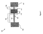
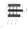
- the FinFETs 100, 200 are designed with asymmetry between the source 101, 201 and drain 102, 202 regions.
- the gate and particularly, the gate conductor 120, 220 is placed closer to the point where the fin 150, 250 merges into a single source strap (see item 101 of Figure 1 ) or increases in width (see item 271 of Figure 2 ) between the gate conductor and source strap.
- the gate conductor 120, 220 is place further from the point where the fin increases in width (see item 272 of Figure 2 ) between the gate conductor and drain strap or from where the fin merges into a single drain strap (see item 102 of Figure 1 ).
- one embodiment of the FinFET structure (100, 200) of the invention comprises parallel semiconductor planes on a substrate that form a source region 101, 201 and a drain region 102, 202.
- Another semiconductor plane i.e., a 3-40nm wide fin 150, 250
- a gate is positioned on the fin 150, 250 between the source 101, 201 and drain regions 102, 202.
- a gate dielectric layer is formed ont he opposing sidewalls of the fin between the source and drain regions.
- a gate conductor 120, 220 is form on the gate dielectric layer.
- the FinFET structure 100, 200 is asymmetrically configured such that a first resistance of the semiconductor fin 150,250 between the source region 101, 201 and the gate conductor 120, 220 is less than a second resistance of the semiconductor fin 150, 250 between the gate conductor 120, 220 and the drain region 102, 202 and such that a first capacitance between the source region 101, 201 and the gate conductor 120, 220 is greater than a second capacitance between the gate conductor 120, 220 and the drain region 102, 202.
- the gate conductor 120 may be positioned on the fin 150 closer to the source region 101 than the drain region 102. Positioning the gate conductor closer to the source region ensures that the first resistance between the gate conductor and the source region is less than the second resistance between the gate conductor and the drain regions. Positioning the gate conductor farther away from the drain region decreases the capacitance between the gate and the drain region.
- the gate conductor can be positioned equidistance 283, 286 from the source 201 and drain 202 regions.
- the fin 250 can be configured with a first portion 251 between the gate conductor 220 and the source region 201 and a second portion 252 between the gate conductor 220 and the drain region 202.
- Both the first portion 251 and second portion 232 can comprise inner sections 261, 262, respectively, adjacent the gate conductor 220 and outer sections 271, 272 adjacent the inner sections 261, 262 (i.e., between the inner section 261 and the source region 201 and between the inner section 262 and the drain region 202).
- the inner sections 261, 262 can have the same width (e.g., an approximately 3-40nm first width 287).
- the outer sections 271, 272 can also have the same width (e.g., an approximately 9-200nm second width 288) that is wider than the first width 287 of the inner sections 261, 262.
- Decreased capacitance between the gate conductor 220 and the drain region 202 as well as decreased resistance between the gate conductor 220 and the source region 201 are provided if the inner section 262 of the second portion 252 is longer than the inner section 261 of the first portion 251. Resistance is decreased between the gate conductor 220 and the source region 201 the closer the first wide section 271 is to the gate conductor 220.
- optimal resistance and capacitance can be achieved if the inner section 261 has a first length 284 that is approximately equal to the first width 287 and if the inner section 262 has a second length 282 that is greater than approximately three times the first width 287.
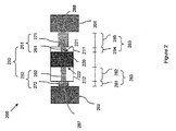
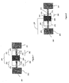
- FIG. 300, 400 of the invention comprises parallel semiconductor planes on a substrate that form a source region 301, 401 and a drain region 302, 402.
- Another semiconductor plane i.e., a 3-40nm wide fin 350, 450
- a gate e.g., comprising a gate dielectric layer and gate conductor 320, 420
- the structures 300, 400 can also comprise spacers 311-312, 411-412 formed over the fin 350, 450 on the opposing sidewalls of the gate conductor 320, 420.
- the FinFET structure 300, 400 of this embodiment is ballasted to prevent destruction at high voltages. As discussed above, at very high voltages FinFETs can enter a mode known as snap-back in which destruction of the FET can result due to current run-away in the hottest region of a transistor channel. This can occur with parallel sets of FinFET having a plurality of fins in which the hottest fin enters thermal run-away, conducting all additional current and ultimately causing the destruction of the FinFETs.
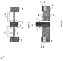
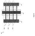
- the structures 300, 400 of the invention provide a ballasted FinFET so that a maximum voltage/current that can be applied to a plurality of FinFETs in parallel (see items 390, 490 of Figures 3c and 4c , respectively) can be increased to a predetermined maximum.
- equal lengths 383 of the semiconductor fin 350 between the gate conductor 320 and the source region 301 and the gate conductor 320 and the drain region 302, respectively, are greater than approximately three to five times a width 388 (e.g., 9-200nm) of the semiconductor fin 350.
- This length 383 can provide enough resistance within the semiconductor fin 350 so that the transistor 300 is operable at a predetermined maximum voltage. Additional resistance for ballasting can be provided if the semiconductor fin 350 is configured with a lesser concentration of dopants in the semiconductor fin than in the source/drain regions 301, 302. Additional resistance can also be provided if the top surface 395 of the semiconductor fin is devoid of a silicide layer 391.
- the source/drain region 301, 302 can be implanted with can be implanted with an N+regioni : 392 and topped with a silicide 391; however, during the manufacturing process silicide 391 and N+region 392 formation in the fin 350 can be blocked.
- the ballasting of the individual FETs (100a-c) prevent the fin with lowest breakdown voltage from entering thermal runaway and conducting all of the excess current, ultimately causing the destruction of all FinFETs 300a-c in the parallel set 390.
- the semiconductor fin 450 can comprise a first portion 451 between the source region 401 and the gate conductor 420 and second portion 452 between the gate conductor 420 and the drain region 402.
- Both the first 451 and second 452 portions comprise inner sections 461, 462, having the same width, e.g., 3-40nm (i.e., first width 487), and the same length, e.g., 9-200nm (i.e., first length 482).
- the inner sections 461, 462 are positioned immediately adjacent the gate conductor 420.
- the first 451 and second 452 portions can also each comprise outer section 471, 472 wide sections between the inner sections 461, 462 and the source/drain region 401, 402. Ballasting can be achieved if the length of the inner sections (i.e., the first length 482) is greater than approximately three to five times their width (i.e., first width 487). Specifically, the length 482 of the inner sections 461, 462 narrow provides resistance within the fin 450 so that the transistor 400 is operable at a predetermined maximum voltage.
- Additional resistance for ballasting can be provided if the inner sections 461, 462 are configured a lesser concentration of source/drain dopants (i.e., p-type or n-type dopants) tha the source/drain regions 401, 402 and if the top surfaces 495 of the inner sections 461, 462 are devoid of an adjacent silicide layer.
- the source/drain regions 401, 402 as well as the outer sections 471., 472 can be implanted with an N+region 492 and topped with a silicide 491; however, during the manufacturing process silicide 491 and N+region 492 formation in the inner sections 461, 462 is blocked by spacers 411, 412.
- ballasting FinFETs 400a-c are formed in a parallel set 490, the ballasting of the individual FETs (400a-c) prevents the fin with lowest breakdown voltage from entering thermal run-away and conducting all of the excess current, and ultimately causing the destruction of all FinFETs 400a-c in the parallel set 490.
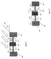
- an asymmetric FinFET 100 incorporates conventional silicon-on-insulator (SOI) FinFET processing techniques.
- the method comprises forming the source/drain regions 101, 102 (500) and forming the approximately 3-40nm semiconductor fin 150 that extends from the source region 101 to the drain region 102 (502).
- the source/drain region and the fin can be lithographically patterned and etched into a silicon layer of an SOI wafer such that the source/drain regions are formed as parallel planes and the fin(s) extend between the source region and the drain region.
- a hard mask may be deposited above the silicon layer.
- Asymmetry is provided by forming a gate (e.g., gate dielectric layer and gate conductor 120) adjacent to the semiconductor fin 150 such that the gate conductor 120 is closer to the source region 101 than the drain region 102 (504).
- a gate e.g., gate dielectric layer and gate conductor 120
- a sacrificial oxide can be grown on the fin and, particularly, on the exposed silicon surfaces of the fin and the source/drain regions and then stripped to remove any irregularities.
- a gate dielectric layer can be grown or deposited on the sidewalls and top surface of the fin.
- a conductive material such as a polysilicon, can be deposited over the fin, lithographically patterned and etched. In this embodiment, the gate conductor that is formed is positioned closer to the source region.
- the asymmetry in the placement of gate conductor 120 between the source and drain region results a first resistance of the semiconductor fin 150 between the source region 101 and the gate conductor 120 that is less than a second resistance of the semiconductor fin 150 between gate conductor 120 and the drain region 102.
- This asymmetry also results in a first capacitance between the source region 101 and the gate conductor 120 that is greater tha a second capacitance between the gate conductor 120 and the drain region 102.
- forming the gate conductor 120 adjacent to the semiconductor fin 150 such that the gate conductor 120 is closer to the source region 101 than the drain region 102 decreases the resistance in the fin 150 between me source region 101 and the gate conductor 120 and decreases the capacitance between the gate conductor 120 and the drain region 102.
- Additional processing can be performed to complete the FinFET 100 (506).
- This additional processing may include, but is not limited to: stripping the optional hard mask by a directional reactive ion etching process; implanting source/drain extensions (i.e., imputing sections of fin between gate conductor and the source/drain regions); forming halos; forming fin spacers; forming spacers on gate sidewalls; implanting N+ into the source/drain regions; forming a silicide layer (e.g., Co, Ni, Etc.) on the top surface of the fin, on the top surface of the source/drain regions, and/or on the top surface of the gate conductor if the gate conductor is formed with a polysilicon material and without a cap; depositing and planarizing an additional dielectric layer, forming gate contacts, forming source/drain contacts, etc. It should be noted that the same processing steps can be used to simultaneously from multiple transistors 100 in which multiple semiconductor fins share the same source/drain strap.
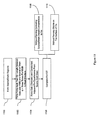
- an embodiment of the present invention is illustrated, describing the method of manufacturing an asymetric FinFET 200 which also incorporates conventional silicon-on-insulator (SOI) FinFET processing techniques.
- the method comprises forming the source/drain regions 201, 202 (600) and forming a narrow semiconductor fin 250 that extends from the source region 201 to the drain region 202 (602), as described in detail above.
- the gate including the gate conductor 220
- the gate can be formed adjacent the semiconductor fin 250 equidistance 283 between the source region 20 1 and the drain region; 202 (604).
- the dimensions of the fin on either side of the gate conductor are adjusted to vary the first resistance within a first portion of the fin between the gate conductor and the source region and a second resistance of a second portion of the fin between the gate conductor and the drain region (605).
- the dimensions of the first portion 251 can be adjusted so that a first inner section 261, having a first width 287 (e.g., 3-40nm), is positioned adjacent to the gate conductor 220 and a first outer section 271, having a second width 288 that is greater than the first width 287, is positioned between the first inner section 261 and the source region 201.
- the dimensions of the second portion 252 can be adjusted to form a second inner section 262 and a second outer section 272.
- the inner sections can each have the same width 287 and the outer sections can have the same 288.
- Asymmetric can be achieved if the second inner section 262 is longer than the first inner section 262, thereby, decreasing the resistance in the fin 250 between the source region 201 and the gate conductor 220 and decreasing the capacitance between the gate conductor 220 and the drain region 201.
- first inner section 261 is formed with a first length 284 that is approximately equal to the first width 287 (e.g., 3-40nm) and the second inner section 262 is formed with a second length 282 that is greater than approximately three to five times the first width 287(e.g., 9-200nm).
- first 211 and second 212 spacers are simultaneously formed immediately on the sides 221, 222 of the gate conductor 220 over the first portion 251 and second portion 252, respectively, of the fin 250 (606, see Figure 7 )).
- the spacers 211, 212 may be formed by growing or depositing an approximately 9-200nm thick silicon dioxide layer on the sides 221, 222 of the gate conductor 220.
- the spacers 211, 212 can initially be formed to have the same thickness 282.
- This thickness 282 should be greater than approximately three to five times the width 287 (i.e., first width) of the fin as originally formed (e.g., 3-40nm).
- the spacers 211, 212 may each be approximately 9-200nm thick. Additionally, the spacers 211, 212 should be formed such that a first exposed section 276 of the first portion 251 of the fin 250 remains between the first spacer 211 and the source region 201 and a second exposed section 275 of the second portion 252 of the fin 250 remains between the second spacer 212 and the drain region 202.
- the size (i.e., thickness 282) of the first spacer 211 is reduced such that the spacer 211 has another thickness 284 that is approximately equal to the first width 287 (608, see Figure 2 ).
- One technique for reducing the thickness of the first spacer comprises masking 277 the second spacer 212 (610, see Figure 8 ) and then isotropically etching the first spacer (612, see Figure 8 ). The etching process etches back not only the top surface 213 of the first spacer 211 but also the exposed sidewall 215 of the first spacer 211, thus, reducing the spacer thickness. Once the first spacer 211 thickness is reduced, the mask 277 is removed (614).
- Another technique for reducing the thickness of the first spacer comprises implanting an inert species 217 (e.g., silicon, argon, xenon, etc) into the silicon dioxide spacers 211, 212 from an angle 216 ( ⁇ 90 degrees) towards the first spacer 211 such that implantation of the second spacer 212 is shadowed (i.e., partially blocked) by the gate conductor 220.
- an inert species 217 e.g., silicon, argon, xenon, etc
- the first spacer 211 receives a greater concentration of the inert material 217 which enhances the etch rate of the first spacer 211 (616, see Figure 9 ).
- first spacer 211 with the greater concentration of the inert species 217 is etched at a faster rate than the second spacer 212 (618, see Figure 10 ).
- the etching process (618) etches back not only the top surface 213 of the first spacer 211 but also the exposed sidewall 215 of the first spacer 211, thus, reducing the spacer thickness.
- additional semiconductor material e.g., silicon, silicon germanium, silicon germanium carbide, etc.
- the process (620) of forming the additional semiconductor material can be accomplished by selectively growing silicon, silicon germanium, or silicon germanium carbide, on the exposed sections 275, 276 of the fin 250 as well as on the silicon source/drain regions.
- This process (620) forms the first and second outer sections 271, 272 (see Figure 2 ).
- the first and second inner sections 261, 262 are those sections of the fin 250 that remain under the first 211 and second 212 spacers, respectively. Additional processing may be performed to complete the FinFET 200 (622 of Figure 6 ), as described in detail above. It should be noted that the same processing steps can be used to simultaneously form multiple transistors 200 in which multiple semiconductor fins share the same source/drain straps.
- an embodiment of the method of manufacturing a fin-type field effect transistor, and particularly, a ballasted FinFET 300 comprises forming the source/drain regions 301, 302 as well as forming the semiconductor fin 350 using conventional FinFET processing technology (1100-1102), as described in detail above.
- a gate including a gate dielectric layer and a gate conductor 320, is formed adjacent to the semiconductor fm such that the gate conductor 320 is equidistance 383 between the source region 301 and the drain region 302 (1104, see detail description of gate formation process above).
- Ballasting can be achieved by forming the gate such that the length 383 of the fm 350 between either the gate conductor 320 and the source region 301 or the gate conductor 320 and the drain region 302 is greater than approximately three times a width 388 of the semiconductor fin 350. This length 383 provides added resistance within the semiconductor fin 350 so that the transistor 300 is operable at a predetermined maximum voltage.
- additional processing steps may be performed to complete FinFET (1106, see detailed description above).
- Additional resistance for ballasting can be provided by forming the semiconductor fin 350 with a lesser concentration of source/drain dopants than the source/drain regions (1108) (e.g., by blocking implantation of an N+region 392 into the fin 350 at process 1106, see Figure 3b ) and without a silicide layer on the top surface 395 of the fin 350 (11 10) (e.g., by blocking formation or the silicide layer 391 on the top surface 395 of the fin 350 at process 1106. see Figure 3b ). It should be noted that the same processing steps can be used to simultaneously form multiple transistros 300 in which multiple semiconductor fins share the same source/drain straps (see Figure 3c ).
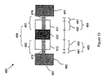
- a method of manufacturing the ballasted FinFET 400 comprises forming the source/drain regions 401, 402 as well as forming a narrow semiconductor fin 450 using conventional FinFET processing technology (1200-1202, see detailed description above).
- a gate including a gate dielectric layer and a gate conductor 420, is formed adjacent to the semiconductor fin 450 such that the gate conductor 420 is equidistance 483 between the source region 401 and the drain region 402 (1204, see detailed description above).
- the dimensions of the im can be adjusted to optimize resistance so that the transistor is operable at a predetermined maximum voltage (1205).
- the dimensions of the fins may be adjusted by forming outer sections of the fin adjacent to the source/drain that are wider than inner sections of the fin adjacent to the gate conductor. Specifically, the dimensions of both a first portion 451 of the fin 450 not covered by the gate conductor 420 that extends between the source region 401 and th gate conductor 420 and a second portion 452 that extends between the gate conductor 420 and the drain region 402 can adjusted. The dimensions can be adjusted so that inner sections 461, 462 that have the same width 487 (i.e., a first width 487) and the same length (i.e., first length 482) are positioned adjacent the gate conductor.
- outer sections 471, 472 have the same width 488 (i.e., second width) and the same length 481 (i.e., second length) and are positioned adjacent the source/drain regions.
- the outer sections 471, 472 are formed such that their width 488 is greater than the width 487 of the inner sections 461, 462. Ballasting is achieved by forming the inner and outer sections so that the length 482 of the inner sections 461,462 is greater than approximately three times the the fin (i.e., first width 487), thereby, providing enough resistance within the first and second inner sections 461, 462 so that the transistor 400 is operable at a pedetermined maximum voltage.
- spacers 411, 412 are formed over the first and second portions 451, 452 of the fin 450 (e.g., on the top surface and opposing sidewalls of the fin 450) immediately adjacent the sides 421, 422 of the gate conductor 420 (1206, see Figure 13 ).
- the spacers 411, 412 can be formed (e.g., by growing or depositing a silicon dioxide) with a thickness 482 that is greater than approximately three to five times the first width 487 (i.e., the width of the fin (e.g., 3-40nm) as initially formed at process (1202)).
- the spacers should also be formed such that first and second exposed sections 476, 475 of the fin 450 remain between the spacers 411, 412 and the source/drain regions 401, 402.
- additional semiconductor material e.g., silicon, silicon germanium, silicon germanium carbide, etc.
- the first and second inner sections 461, 462 are those sections of the fin 450 that remain under the spacers 411, 412.
- the length of the inner sections is a function of the thickness of the spacers.
- Additional processing steps may be performed to complete FinFET (12010), as described in detail above. Additional resistance or ballasting can be provided by forming the first and second inner sections 461, 462 of the semiconductor fin 450 with a source/drain dopant concentration that is less than that of the source/drain regions (1212) (e.g., by blocking implantation of an N-region 492 into the fin 450 at process 1210, see Figure 4b ) and by the inner sections without a silicide layer (1214) (e.g., by blocking formation of the silicide layer 491 on the top surface 495 of the fin 450 at process 1210, see Figure 4b ). It should be noted that the same processing steps can be used to simultaneously form multiple transistors 400 in which multiple semiconductor fins share the same source/drain straps (see Figure 4c ).
- FinFET fin-type field effect transistor
- FinFET drive current is optimised by configuring the FinFET asymmetrically to decrease fin resistance between the gate and the source region and to decrease capacitance between the gate and the drain region. Due to this simultaneously low source-gate resistance and low drain-gate capacitance, such asymmetric FinFETS can provide circuits having higher switching speed and reduced power. This also translates into physically smaller circuits, and hence lower cost circuits, same fewer fins can provide equivalent speed.
- device destruction at high voltages is prevented by ballasting the FinFET.
- resistance is optimized in the fin between the gate and both the source and drain regions (e.g., by increasing fin length, by blocking source/drain implant from the fin, and by blocking silicide formation on the top surface of the fin) so that the FinFET is operable at a predetermined maximum voltage.
- Such ballasted FinFETs provide for higher reliability at higher operation voltage, and can avoid special, costly processing steps otherwise required to add special high-voltage transistors to a circuit.
Landscapes
- Thin Film Transistor (AREA)
- Insulated Gate Type Field-Effect Transistor (AREA)
- Bipolar Transistors (AREA)
Applications Claiming Priority (2)
| Application Number | Priority Date | Filing Date | Title |
|---|---|---|---|
| US11/161,442 US7348642B2 (en) | 2005-08-03 | 2005-08-03 | Fin-type field effect transistor |
| PCT/US2006/028465 WO2007019023A2 (en) | 2005-08-03 | 2006-07-21 | Fin-type field effect transistor |
Publications (3)
| Publication Number | Publication Date |
|---|---|
| EP1920467A2 EP1920467A2 (en) | 2008-05-14 |
| EP1920467A4 EP1920467A4 (en) | 2011-03-02 |
| EP1920467B1 true EP1920467B1 (en) | 2012-02-01 |
Family
ID=37716900
Family Applications (1)
| Application Number | Title | Priority Date | Filing Date |
|---|---|---|---|
| EP06788172A Active EP1920467B1 (en) | 2005-08-03 | 2006-07-21 | Fin-type field effect transistor |
Country Status (8)
Families Citing this family (67)
| Publication number | Priority date | Publication date | Assignee | Title |
|---|---|---|---|---|
| US7456476B2 (en) | 2003-06-27 | 2008-11-25 | Intel Corporation | Nonplanar semiconductor device with partially or fully wrapped around gate electrode and methods of fabrication |
| US7268058B2 (en) * | 2004-01-16 | 2007-09-11 | Intel Corporation | Tri-gate transistors and methods to fabricate same |
| US7042009B2 (en) | 2004-06-30 | 2006-05-09 | Intel Corporation | High mobility tri-gate devices and methods of fabrication |
| US7332439B2 (en) * | 2004-09-29 | 2008-02-19 | Intel Corporation | Metal gate transistors with epitaxial source and drain regions |
| US20060086977A1 (en) | 2004-10-25 | 2006-04-27 | Uday Shah | Nonplanar device with thinned lower body portion and method of fabrication |
| US7518196B2 (en) | 2005-02-23 | 2009-04-14 | Intel Corporation | Field effect transistor with narrow bandgap source and drain regions and method of fabrication |
| US7858481B2 (en) | 2005-06-15 | 2010-12-28 | Intel Corporation | Method for fabricating transistor with thinned channel |
| US7547637B2 (en) | 2005-06-21 | 2009-06-16 | Intel Corporation | Methods for patterning a semiconductor film |
| US7279375B2 (en) * | 2005-06-30 | 2007-10-09 | Intel Corporation | Block contact architectures for nanoscale channel transistors |
| US7348642B2 (en) * | 2005-08-03 | 2008-03-25 | International Business Machines Corporation | Fin-type field effect transistor |
| US7595245B2 (en) * | 2005-08-12 | 2009-09-29 | Texas Instruments Incorporated | Semiconductor device having a gate electrode material feature located adjacent a gate width side of its gate electrode and a method of manufacture therefor |
| DE102005039365B4 (de) * | 2005-08-19 | 2022-02-10 | Infineon Technologies Ag | Gate-gesteuertes Fin-Widerstandselement, welches als pinch - resistor arbeitet, zur Verwendung als ESD-Schutzelement in einem elektrischen Schaltkreis und Einrichtung zum Schutz vor elektrostatischen Entladungen in einem elektrischen Schaltkreis |
| US20070090416A1 (en) | 2005-09-28 | 2007-04-26 | Doyle Brian S | CMOS devices with a single work function gate electrode and method of fabrication |
| US7485503B2 (en) | 2005-11-30 | 2009-02-03 | Intel Corporation | Dielectric interface for group III-V semiconductor device |
| US8143646B2 (en) | 2006-08-02 | 2012-03-27 | Intel Corporation | Stacking fault and twin blocking barrier for integrating III-V on Si |
| JP2008177278A (ja) * | 2007-01-17 | 2008-07-31 | Toshiba Corp | スタティック型半導体記憶装置 |
| KR100887007B1 (ko) | 2007-10-12 | 2009-03-04 | 주식회사 동부하이텍 | Ldi의 알-스트링내 폴리 패턴 형성 방법 및 구조 |
| US7994612B2 (en) * | 2008-04-21 | 2011-08-09 | International Business Machines Corporation | FinFETs single-sided implant formation |
| WO2009130629A1 (en) * | 2008-04-23 | 2009-10-29 | Nxp B.V. | A fin fet and a method of manufacturing a fin fet |
| US8362566B2 (en) | 2008-06-23 | 2013-01-29 | Intel Corporation | Stress in trigate devices using complimentary gate fill materials |
| US7781283B2 (en) * | 2008-08-15 | 2010-08-24 | International Business Machines Corporation | Split-gate DRAM with MuGFET, design structure, and method of manufacture |
| US7979836B2 (en) * | 2008-08-15 | 2011-07-12 | International Business Machines Corporation | Split-gate DRAM with MuGFET, design structure, and method of manufacture |
| US8331068B2 (en) | 2009-02-19 | 2012-12-11 | Taiwan Semiconductor Manufacturing Company, Ltd. | ESD protection for FinFETs |
| US8184472B2 (en) | 2009-03-13 | 2012-05-22 | International Business Machines Corporation | Split-gate DRAM with lateral control-gate MuGFET |
| US8202780B2 (en) * | 2009-07-31 | 2012-06-19 | International Business Machines Corporation | Method for manufacturing a FinFET device comprising a mask to define a gate perimeter and another mask to define fin regions |
| US8946028B2 (en) * | 2009-10-06 | 2015-02-03 | International Business Machines Corporation | Merged FinFETs and method of manufacturing the same |
| US8716797B2 (en) * | 2009-11-03 | 2014-05-06 | International Business Machines Corporation | FinFET spacer formation by oriented implantation |
| US8174055B2 (en) * | 2010-02-17 | 2012-05-08 | Globalfoundries Inc. | Formation of FinFET gate spacer |
| US8513102B2 (en) | 2010-11-08 | 2013-08-20 | Leonard Forbes | Reduction of random telegraph signal (RTS) and 1/f noise in silicon MOS devices, circuits, and sensors |
| JP2012243971A (ja) * | 2011-05-20 | 2012-12-10 | Sony Corp | ブートストラップ回路、インバータ回路、走査回路、表示装置、及び、電子機器 |
| CN102760735B (zh) * | 2011-06-21 | 2015-06-17 | 钰创科技股份有限公司 | 动态记忆体结构 |
| US8595661B2 (en) * | 2011-07-29 | 2013-11-26 | Synopsys, Inc. | N-channel and p-channel finFET cell architecture |
| US8466027B2 (en) * | 2011-09-08 | 2013-06-18 | Taiwan Semiconductor Manufacturing Company, Ltd. | Silicide formation and associated devices |
| KR101805634B1 (ko) * | 2011-11-15 | 2017-12-08 | 삼성전자 주식회사 | Ⅲ-ⅴ족 배리어를 포함하는 반도체 소자 및 그 제조방법 |
| CN103165428B (zh) * | 2011-12-14 | 2015-12-09 | 中芯国际集成电路制造(上海)有限公司 | 制作半导体器件的方法 |
| US8901659B2 (en) * | 2012-02-09 | 2014-12-02 | International Business Machines Corporation | Tapered nanowire structure with reduced off current |
| US8637371B2 (en) | 2012-02-16 | 2014-01-28 | International Business Machines Corporation | Non-planar MOSFET structures with asymmetric recessed source drains and methods for making the same |
| US8927432B2 (en) * | 2012-06-14 | 2015-01-06 | International Business Machines Corporation | Continuously scalable width and height semiconductor fins |
| KR20140040543A (ko) * | 2012-09-26 | 2014-04-03 | 삼성전자주식회사 | 핀 구조의 전계효과 트랜지스터, 이를 포함하는 메모리 장치 및 그 반도체 장치 |
| CN103779217A (zh) * | 2012-10-18 | 2014-05-07 | 中芯国际集成电路制造(上海)有限公司 | 一种鳍片型场效应晶体管及其制作方法 |
| CN103811338B (zh) * | 2012-11-08 | 2016-12-21 | 中芯国际集成电路制造(上海)有限公司 | 一种半导体器件及其制备方法 |
| US9123654B2 (en) * | 2013-02-15 | 2015-09-01 | International Business Machines Corporation | Trilayer SIT process with transfer layer for FINFET patterning |
| US9231106B2 (en) * | 2013-03-08 | 2016-01-05 | Taiwan Semiconductor Manufacturing Company, Ltd. | FinFET with an asymmetric source/drain structure and method of making same |
| CN104103319B (zh) * | 2013-04-11 | 2017-08-25 | 中芯国际集成电路制造(上海)有限公司 | 反熔丝电路及其编程方法、反熔丝结构 |
| KR102089682B1 (ko) | 2013-07-15 | 2020-03-16 | 삼성전자 주식회사 | 반도체 장치 및 이의 제조 방법 |
| US9484460B2 (en) | 2013-09-19 | 2016-11-01 | Taiwan Semiconductor Manufacturing Company Limited | Semiconductor device having gate dielectric surrounding at least some of channel region and gate electrode surrounding at least some of gate dielectric |
| US9190466B2 (en) | 2013-12-27 | 2015-11-17 | International Business Machines Corporation | Independent gate vertical FinFET structure |
| US9691763B2 (en) | 2013-12-27 | 2017-06-27 | International Business Machines Corporation | Multi-gate FinFET semiconductor device with flexible design width |
| US9633906B2 (en) | 2014-01-24 | 2017-04-25 | International Business Machines Corporation | Gate structure cut after formation of epitaxial active regions |
| EP3123517A4 (en) | 2014-03-24 | 2017-11-29 | Intel Corporation | Techniques for achieving multiple transistor fin dimensions on a single die |
| US9318574B2 (en) * | 2014-06-18 | 2016-04-19 | International Business Machines Corporation | Method and structure for enabling high aspect ratio sacrificial gates |
| US9281065B2 (en) | 2014-08-11 | 2016-03-08 | Empire Technology Development Llc | Low-power nonvolatile memory cells with select gates |
| JP6373686B2 (ja) * | 2014-08-22 | 2018-08-15 | ルネサスエレクトロニクス株式会社 | 半導体装置 |
| US10559690B2 (en) | 2014-09-18 | 2020-02-11 | International Business Machines Corporation | Embedded source/drain structure for tall FinFET and method of formation |
| KR102168302B1 (ko) | 2014-11-21 | 2020-10-22 | 삼성전자주식회사 | 3차원 채널을 이용하는 반도체 장치 |
| KR102320049B1 (ko) | 2015-02-26 | 2021-11-01 | 삼성전자주식회사 | 경사진 활성 영역을 갖는 반도체 소자 |
| US10018515B2 (en) * | 2015-09-16 | 2018-07-10 | Qualcomm Incorporated | Transistor temperature sensing |
| US9484306B1 (en) | 2015-11-17 | 2016-11-01 | International Business Machines Corporation | MOSFET with asymmetric self-aligned contact |
| TWI594421B (zh) * | 2016-06-28 | 2017-08-01 | 瑞昱半導體股份有限公司 | 鰭式場效電晶體及其製造方法 |
| CN107579116A (zh) * | 2016-07-05 | 2018-01-12 | 瑞昱半导体股份有限公司 | 鳍式场效晶体管及其制造方法 |
| KR101859587B1 (ko) | 2016-12-30 | 2018-05-18 | 서울시립대학교 산학협력단 | 네거티브 캐패시턴스 핀펫 소자 및 제조 방법 |
| US10475790B2 (en) | 2017-09-28 | 2019-11-12 | Taiwan Semiconductor Manufacturing Co., Ltd. | Asymmetric gate pitch |
| KR102446403B1 (ko) * | 2018-06-22 | 2022-09-21 | 삼성전자주식회사 | 반도체 장치, 반도체 장치의 제조 방법 및 반도체 장치의 레이아웃 디자인 방법 |
| JP6612937B2 (ja) * | 2018-07-18 | 2019-11-27 | ルネサスエレクトロニクス株式会社 | 半導体装置 |
| US11060846B2 (en) * | 2018-12-19 | 2021-07-13 | Kla Corporation | Scatterometry based methods and systems for measurement of strain in semiconductor structures |
| KR102813445B1 (ko) | 2019-10-02 | 2025-05-27 | 삼성전자주식회사 | 집적회로 소자 및 그 제조 방법 |
| US11670675B2 (en) | 2020-12-04 | 2023-06-06 | United Semiconductor Japan Co., Ltd. | Semiconductor device |
Family Cites Families (39)
| Publication number | Priority date | Publication date | Assignee | Title |
|---|---|---|---|---|
| US539896A (en) * | 1895-05-28 | John graves | ||
| JPS6226665A (ja) | 1985-07-26 | 1987-02-04 | Hitachi Ltd | 磁気デイスク駆動装置 |
| JPS6226865A (ja) | 1985-07-29 | 1987-02-04 | New Japan Radio Co Ltd | 電界効果トランジスタ |
| JPS62132366A (ja) | 1985-12-04 | 1987-06-15 | Nec Corp | 縦型電界効果トランジスタの製造方法 |
| JPS63308962A (ja) * | 1987-06-11 | 1988-12-16 | Sanyo Electric Co Ltd | 半導体装置の製造方法 |
| US4907041A (en) * | 1988-09-16 | 1990-03-06 | Xerox Corporation | Intra-gate offset high voltage thin film transistor with misalignment immunity |
| US5399896A (en) | 1992-09-29 | 1995-03-21 | Mitsubishi Denki Kabushiki Kaisha | FET with a T-shaped gate of a particular structure |
| US5985724A (en) | 1996-10-01 | 1999-11-16 | Advanced Micro Devices, Inc. | Method for forming asymmetrical p-channel transistor having nitrided oxide patterned to selectively form a sidewall spacer |
| US20020036328A1 (en) | 1998-11-16 | 2002-03-28 | William R. Richards, Jr. | Offset drain fermi-threshold field effect transistors |
| US6291325B1 (en) | 1998-11-18 | 2001-09-18 | Sharp Laboratories Of America, Inc. | Asymmetric MOS channel structure with drain extension and method for same |
| JP3543946B2 (ja) * | 2000-04-14 | 2004-07-21 | 日本電気株式会社 | 電界効果型トランジスタ及びその製造方法 |
| EP1292989A1 (en) | 2000-05-10 | 2003-03-19 | Koninklijke Philips Electronics N.V. | A semiconductor device |
| US6413802B1 (en) | 2000-10-23 | 2002-07-02 | The Regents Of The University Of California | Finfet transistor structures having a double gate channel extending vertically from a substrate and methods of manufacture |
| JP3729082B2 (ja) * | 2001-04-25 | 2005-12-21 | 日本電信電話株式会社 | 半導体保護回路 |
| US6525354B2 (en) | 2001-04-27 | 2003-02-25 | Fujitsu Limited | FET circuit block with reduced self-heating |
| JP2002343806A (ja) | 2001-05-15 | 2002-11-29 | Mitsubishi Electric Corp | 半導体装置およびその製造方法 |
| US6492212B1 (en) * | 2001-10-05 | 2002-12-10 | International Business Machines Corporation | Variable threshold voltage double gated transistors and method of fabrication |
| US6967351B2 (en) * | 2001-12-04 | 2005-11-22 | International Business Machines Corporation | Finfet SRAM cell using low mobility plane for cell stability and method for forming |
| JP3605086B2 (ja) | 2002-03-29 | 2004-12-22 | 株式会社東芝 | 電界効果トランジスタ |
| US6664582B2 (en) * | 2002-04-12 | 2003-12-16 | International Business Machines Corporation | Fin memory cell and method of fabrication |
| US7074623B2 (en) | 2002-06-07 | 2006-07-11 | Amberwave Systems Corporation | Methods of forming strained-semiconductor-on-insulator finFET device structures |
| US6706571B1 (en) | 2002-10-22 | 2004-03-16 | Advanced Micro Devices, Inc. | Method for forming multiple structures in a semiconductor device |
| US6864519B2 (en) | 2002-11-26 | 2005-03-08 | Taiwan Semiconductor Manufacturing Co., Ltd. | CMOS SRAM cell configured using multiple-gate transistors |
| US7259425B2 (en) | 2003-01-23 | 2007-08-21 | Advanced Micro Devices, Inc. | Tri-gate and gate around MOSFET devices and methods for making same |
| US6800885B1 (en) | 2003-03-12 | 2004-10-05 | Advance Micro Devices, Inc. | Asymmetrical double gate or all-around gate MOSFET devices and methods for making same |
| US6764884B1 (en) * | 2003-04-03 | 2004-07-20 | Advanced Micro Devices, Inc. | Method for forming a gate in a FinFET device and thinning a fin in a channel region of the FinFET device |
| US7456476B2 (en) * | 2003-06-27 | 2008-11-25 | Intel Corporation | Nonplanar semiconductor device with partially or fully wrapped around gate electrode and methods of fabrication |
| US6897111B2 (en) | 2003-07-28 | 2005-05-24 | Chartered Semiconductor Manufacturing Ltd. | Method using quasi-planar double gated fin field effect transistor process for the fabrication of a thyristor-based static read/write random-access memory |
| JP2005086024A (ja) * | 2003-09-09 | 2005-03-31 | Toshiba Corp | 半導体装置及びその製造方法 |
| JP2005142289A (ja) * | 2003-11-05 | 2005-06-02 | Toshiba Corp | 半導体記憶装置 |
| JP3962009B2 (ja) * | 2003-12-05 | 2007-08-22 | 株式会社東芝 | 半導体装置の製造方法 |
| US7115947B2 (en) * | 2004-03-18 | 2006-10-03 | International Business Machines Corporation | Multiple dielectric finfet structure and method |
| US7154118B2 (en) * | 2004-03-31 | 2006-12-26 | Intel Corporation | Bulk non-planar transistor having strained enhanced mobility and methods of fabrication |
| US7176092B2 (en) * | 2004-04-16 | 2007-02-13 | Taiwan Semiconductor Manufacturing Company | Gate electrode for a semiconductor fin device |
| US7148540B2 (en) * | 2004-06-28 | 2006-12-12 | Agere Systems Inc. | Graded conductive structure for use in a metal-oxide-semiconductor device |
| US20060071270A1 (en) * | 2004-09-29 | 2006-04-06 | Shibib Muhammed A | Metal-oxide-semiconductor device having trenched diffusion region and method of forming same |
| ATE392716T1 (de) * | 2005-02-21 | 2008-05-15 | Imec Inter Uni Micro Electr | Halbleiterspeicherbauelement mit schwebendem körper und herstellungsverfahren desselben |
| US7176537B2 (en) * | 2005-05-23 | 2007-02-13 | Taiwan Semiconductor Manufacturing Company, Ltd. | High performance CMOS with metal-gate and Schottky source/drain |
| US7348642B2 (en) * | 2005-08-03 | 2008-03-25 | International Business Machines Corporation | Fin-type field effect transistor |
-
2005
- 2005-08-03 US US11/161,442 patent/US7348642B2/en not_active Expired - Lifetime
-
2006
- 2006-07-21 WO PCT/US2006/028465 patent/WO2007019023A2/en active Application Filing
- 2006-07-21 EP EP06788172A patent/EP1920467B1/en active Active
- 2006-07-21 CN CN2006800285758A patent/CN101443912B/zh active Active
- 2006-07-21 JP JP2008525007A patent/JP5220604B2/ja not_active Expired - Fee Related
- 2006-07-21 KR KR1020087004466A patent/KR101027173B1/ko not_active Expired - Fee Related
- 2006-07-21 AT AT06788172T patent/ATE544182T1/de active
- 2006-08-02 TW TW095128273A patent/TWI397999B/zh active
-
2007
- 2007-12-13 US US11/955,579 patent/US8129773B2/en active Active
-
2008
- 2008-01-10 US US11/972,412 patent/US8106439B2/en active Active
-
2012
- 2012-01-30 US US13/361,050 patent/US8524547B2/en not_active Expired - Lifetime
Also Published As
| Publication number | Publication date |
|---|---|
| JP5220604B2 (ja) | 2013-06-26 |
| CN101443912A (zh) | 2009-05-27 |
| EP1920467A4 (en) | 2011-03-02 |
| US20080124868A1 (en) | 2008-05-29 |
| WO2007019023A3 (en) | 2008-11-13 |
| US8524547B2 (en) | 2013-09-03 |
| ATE544182T1 (de) | 2012-02-15 |
| CN101443912B (zh) | 2011-03-23 |
| TW200717805A (en) | 2007-05-01 |
| EP1920467A2 (en) | 2008-05-14 |
| US8106439B2 (en) | 2012-01-31 |
| US20080087968A1 (en) | 2008-04-17 |
| US8129773B2 (en) | 2012-03-06 |
| US20120129304A1 (en) | 2012-05-24 |
| KR101027173B1 (ko) | 2011-04-05 |
| US7348642B2 (en) | 2008-03-25 |
| KR20080030110A (ko) | 2008-04-03 |
| TWI397999B (zh) | 2013-06-01 |
| US20070029624A1 (en) | 2007-02-08 |
| JP2009503893A (ja) | 2009-01-29 |
| WO2007019023A2 (en) | 2007-02-15 |
Similar Documents
| Publication | Publication Date | Title |
|---|---|---|
| EP1920467B1 (en) | Fin-type field effect transistor | |
| US6706571B1 (en) | Method for forming multiple structures in a semiconductor device | |
| KR100212693B1 (ko) | 규소/규소게르마늄 모스 전계 트랜지스터 및 그 제조방법 | |
| JP5869753B2 (ja) | 埋め込み拡張領域を有するsoiトランジスタ、及びその形成方法 | |
| US6709982B1 (en) | Double spacer FinFET formation | |
| US7208356B2 (en) | Method of manufacturing multiple-gate MOS transistor having an improved channel structure | |
| US7105934B2 (en) | FinFET with low gate capacitance and low extrinsic resistance | |
| US6580134B1 (en) | Field effect transistors having elevated source/drain regions | |
| US20110042724A1 (en) | Trenched mosfets with part of the device formed on a (110) crystal plane | |
| US7247896B2 (en) | Semiconductor devices having a field effect transistor and methods of fabricating the same | |
| US8889518B2 (en) | LDMOS transistor with asymmetric spacer as gate | |
| JP2006310772A (ja) | Fin型チャネルトランジスタおよびその製造方法 | |
| US7335945B2 (en) | Multi-gate MOS transistor and method of manufacturing the same | |
| JP2006507684A (ja) | 2トランジスタnorデバイス | |
| JP2006286953A (ja) | 半導体装置およびその製造方法 | |
| US10522538B1 (en) | Using source/drain contact cap during gate cut | |
| CN113410231A (zh) | 具有分段外延半导体层的晶体管 | |
| US11374002B2 (en) | Transistors with hybrid source/drain regions | |
| US11239366B2 (en) | Transistors with an asymmetrical source and drain | |
| KR100485004B1 (ko) | 에스오아이 반도체 소자 및 그 제조 방법 | |
| KR20040060487A (ko) | 반도체 장치의 트렌지스터 형성 방법 | |
| JPH0786307A (ja) | 電界効果トランジスタ及びその製造方法 | |
| KR20040008451A (ko) | 트랜지스터의 제조 방법 |
Legal Events
| Date | Code | Title | Description |
|---|---|---|---|
| PUAI | Public reference made under article 153(3) epc to a published international application that has entered the european phase |
Free format text: ORIGINAL CODE: 0009012 |
|
| 17P | Request for examination filed |
Effective date: 20080229 |
|
| AK | Designated contracting states |
Kind code of ref document: A2 Designated state(s): AT BE BG CH CY CZ DE DK EE ES FI FR GB GR HU IE IS IT LI LT LU LV MC NL PL PT RO SE SI SK TR |
|
| AX | Request for extension of the european patent |
Extension state: AL BA HR MK RS |
|
| R17D | Deferred search report published (corrected) |
Effective date: 20081113 |
|
| RIC1 | Information provided on ipc code assigned before grant |
Ipc: H01L 21/336 20060101ALI20081215BHEP Ipc: H01L 29/06 20060101ALI20081215BHEP Ipc: H01L 29/76 20060101ALI20081215BHEP Ipc: H01L 27/108 20060101AFI20081215BHEP |
|
| A4 | Supplementary search report drawn up and despatched |
Effective date: 20110127 |
|
| 17Q | First examination report despatched |
Effective date: 20110512 |
|
| REG | Reference to a national code |
Ref country code: DE Ref legal event code: R079 Ref document number: 602006027444 Country of ref document: DE Free format text: PREVIOUS MAIN CLASS: H01L0027108000 Ipc: H01L0029780000 |
|
| GRAP | Despatch of communication of intention to grant a patent |
Free format text: ORIGINAL CODE: EPIDOSNIGR1 |
|
| RIC1 | Information provided on ipc code assigned before grant |
Ipc: H01L 21/336 20060101ALI20110906BHEP Ipc: H01L 29/78 20060101AFI20110906BHEP |
|
| DAX | Request for extension of the european patent (deleted) | ||
| GRAS | Grant fee paid |
Free format text: ORIGINAL CODE: EPIDOSNIGR3 |
|
| GRAA | (expected) grant |
Free format text: ORIGINAL CODE: 0009210 |
|
| AK | Designated contracting states |
Kind code of ref document: B1 Designated state(s): AT BE BG CH CY CZ DE DK EE ES FI FR GB GR HU IE IS IT LI LT LU LV MC NL PL PT RO SE SI SK TR |
|
| REG | Reference to a national code |
Ref country code: GB Ref legal event code: FG4D |
|
| REG | Reference to a national code |
Ref country code: CH Ref legal event code: NV Representative=s name: IBM RESEARCH GMBH ZURICH RESEARCH LABORATORY INTEL Ref country code: CH Ref legal event code: EP Ref country code: AT Ref legal event code: REF Ref document number: 544182 Country of ref document: AT Kind code of ref document: T Effective date: 20120215 |
|
| REG | Reference to a national code |
Ref country code: DE Ref legal event code: R084 Ref document number: 602006027444 Country of ref document: DE |
|
| REG | Reference to a national code |
Ref country code: GB Ref legal event code: 746 Effective date: 20120228 |
|
| REG | Reference to a national code |
Ref country code: DE Ref legal event code: R096 Ref document number: 602006027444 Country of ref document: DE Effective date: 20120329 |
|
| REG | Reference to a national code |
Ref country code: DE Ref legal event code: R084 Ref document number: 602006027444 Country of ref document: DE Effective date: 20120307 |
|
| REG | Reference to a national code |
Ref country code: NL Ref legal event code: VDEP Effective date: 20120201 |
|
| LTIE | Lt: invalidation of european patent or patent extension |
Effective date: 20120201 |
|
| PG25 | Lapsed in a contracting state [announced via postgrant information from national office to epo] |
Ref country code: IS Free format text: LAPSE BECAUSE OF FAILURE TO SUBMIT A TRANSLATION OF THE DESCRIPTION OR TO PAY THE FEE WITHIN THE PRESCRIBED TIME-LIMIT Effective date: 20120601 Ref country code: NL Free format text: LAPSE BECAUSE OF FAILURE TO SUBMIT A TRANSLATION OF THE DESCRIPTION OR TO PAY THE FEE WITHIN THE PRESCRIBED TIME-LIMIT Effective date: 20120201 Ref country code: LT Free format text: LAPSE BECAUSE OF FAILURE TO SUBMIT A TRANSLATION OF THE DESCRIPTION OR TO PAY THE FEE WITHIN THE PRESCRIBED TIME-LIMIT Effective date: 20120201 |
|
| PG25 | Lapsed in a contracting state [announced via postgrant information from national office to epo] |
Ref country code: LV Free format text: LAPSE BECAUSE OF FAILURE TO SUBMIT A TRANSLATION OF THE DESCRIPTION OR TO PAY THE FEE WITHIN THE PRESCRIBED TIME-LIMIT Effective date: 20120201 Ref country code: BE Free format text: LAPSE BECAUSE OF FAILURE TO SUBMIT A TRANSLATION OF THE DESCRIPTION OR TO PAY THE FEE WITHIN THE PRESCRIBED TIME-LIMIT Effective date: 20120201 Ref country code: PL Free format text: LAPSE BECAUSE OF FAILURE TO SUBMIT A TRANSLATION OF THE DESCRIPTION OR TO PAY THE FEE WITHIN THE PRESCRIBED TIME-LIMIT Effective date: 20120201 Ref country code: PT Free format text: LAPSE BECAUSE OF FAILURE TO SUBMIT A TRANSLATION OF THE DESCRIPTION OR TO PAY THE FEE WITHIN THE PRESCRIBED TIME-LIMIT Effective date: 20120601 Ref country code: GR Free format text: LAPSE BECAUSE OF FAILURE TO SUBMIT A TRANSLATION OF THE DESCRIPTION OR TO PAY THE FEE WITHIN THE PRESCRIBED TIME-LIMIT Effective date: 20120502 Ref country code: FI Free format text: LAPSE BECAUSE OF FAILURE TO SUBMIT A TRANSLATION OF THE DESCRIPTION OR TO PAY THE FEE WITHIN THE PRESCRIBED TIME-LIMIT Effective date: 20120201 |
|
| REG | Reference to a national code |
Ref country code: AT Ref legal event code: MK05 Ref document number: 544182 Country of ref document: AT Kind code of ref document: T Effective date: 20120201 |
|
| PG25 | Lapsed in a contracting state [announced via postgrant information from national office to epo] |
Ref country code: CY Free format text: LAPSE BECAUSE OF FAILURE TO SUBMIT A TRANSLATION OF THE DESCRIPTION OR TO PAY THE FEE WITHIN THE PRESCRIBED TIME-LIMIT Effective date: 20120201 |
|
| PG25 | Lapsed in a contracting state [announced via postgrant information from national office to epo] |
Ref country code: DK Free format text: LAPSE BECAUSE OF FAILURE TO SUBMIT A TRANSLATION OF THE DESCRIPTION OR TO PAY THE FEE WITHIN THE PRESCRIBED TIME-LIMIT Effective date: 20120201 Ref country code: CZ Free format text: LAPSE BECAUSE OF FAILURE TO SUBMIT A TRANSLATION OF THE DESCRIPTION OR TO PAY THE FEE WITHIN THE PRESCRIBED TIME-LIMIT Effective date: 20120201 Ref country code: EE Free format text: LAPSE BECAUSE OF FAILURE TO SUBMIT A TRANSLATION OF THE DESCRIPTION OR TO PAY THE FEE WITHIN THE PRESCRIBED TIME-LIMIT Effective date: 20120201 Ref country code: SI Free format text: LAPSE BECAUSE OF FAILURE TO SUBMIT A TRANSLATION OF THE DESCRIPTION OR TO PAY THE FEE WITHIN THE PRESCRIBED TIME-LIMIT Effective date: 20120201 Ref country code: RO Free format text: LAPSE BECAUSE OF FAILURE TO SUBMIT A TRANSLATION OF THE DESCRIPTION OR TO PAY THE FEE WITHIN THE PRESCRIBED TIME-LIMIT Effective date: 20120201 Ref country code: SE Free format text: LAPSE BECAUSE OF FAILURE TO SUBMIT A TRANSLATION OF THE DESCRIPTION OR TO PAY THE FEE WITHIN THE PRESCRIBED TIME-LIMIT Effective date: 20120201 |
|
| PG25 | Lapsed in a contracting state [announced via postgrant information from national office to epo] |
Ref country code: SK Free format text: LAPSE BECAUSE OF FAILURE TO SUBMIT A TRANSLATION OF THE DESCRIPTION OR TO PAY THE FEE WITHIN THE PRESCRIBED TIME-LIMIT Effective date: 20120201 Ref country code: IT Free format text: LAPSE BECAUSE OF FAILURE TO SUBMIT A TRANSLATION OF THE DESCRIPTION OR TO PAY THE FEE WITHIN THE PRESCRIBED TIME-LIMIT Effective date: 20120201 |
|
| PLBE | No opposition filed within time limit |
Free format text: ORIGINAL CODE: 0009261 |
|
| STAA | Information on the status of an ep patent application or granted ep patent |
Free format text: STATUS: NO OPPOSITION FILED WITHIN TIME LIMIT |
|
| 26N | No opposition filed |
Effective date: 20121105 |
|
| PG25 | Lapsed in a contracting state [announced via postgrant information from national office to epo] |
Ref country code: AT Free format text: LAPSE BECAUSE OF FAILURE TO SUBMIT A TRANSLATION OF THE DESCRIPTION OR TO PAY THE FEE WITHIN THE PRESCRIBED TIME-LIMIT Effective date: 20120201 |
|
| PG25 | Lapsed in a contracting state [announced via postgrant information from national office to epo] |
Ref country code: MC Free format text: LAPSE BECAUSE OF NON-PAYMENT OF DUE FEES Effective date: 20120731 |
|
| REG | Reference to a national code |
Ref country code: DE Ref legal event code: R097 Ref document number: 602006027444 Country of ref document: DE Effective date: 20121105 Ref country code: CH Ref legal event code: PL |
|
| REG | Reference to a national code |
Ref country code: FR Ref legal event code: ST Effective date: 20130329 |
|
| PG25 | Lapsed in a contracting state [announced via postgrant information from national office to epo] |
Ref country code: LI Free format text: LAPSE BECAUSE OF NON-PAYMENT OF DUE FEES Effective date: 20120731 Ref country code: ES Free format text: LAPSE BECAUSE OF FAILURE TO SUBMIT A TRANSLATION OF THE DESCRIPTION OR TO PAY THE FEE WITHIN THE PRESCRIBED TIME-LIMIT Effective date: 20120512 Ref country code: FR Free format text: LAPSE BECAUSE OF NON-PAYMENT OF DUE FEES Effective date: 20120731 Ref country code: CH Free format text: LAPSE BECAUSE OF NON-PAYMENT OF DUE FEES Effective date: 20120731 |
|
| REG | Reference to a national code |
Ref country code: IE Ref legal event code: MM4A |
|
| PG25 | Lapsed in a contracting state [announced via postgrant information from national office to epo] |
Ref country code: BG Free format text: LAPSE BECAUSE OF FAILURE TO SUBMIT A TRANSLATION OF THE DESCRIPTION OR TO PAY THE FEE WITHIN THE PRESCRIBED TIME-LIMIT Effective date: 20120501 Ref country code: IE Free format text: LAPSE BECAUSE OF NON-PAYMENT OF DUE FEES Effective date: 20120721 |
|
| PG25 | Lapsed in a contracting state [announced via postgrant information from national office to epo] |
Ref country code: TR Free format text: LAPSE BECAUSE OF FAILURE TO SUBMIT A TRANSLATION OF THE DESCRIPTION OR TO PAY THE FEE WITHIN THE PRESCRIBED TIME-LIMIT Effective date: 20120201 |
|
| PG25 | Lapsed in a contracting state [announced via postgrant information from national office to epo] |
Ref country code: LU Free format text: LAPSE BECAUSE OF NON-PAYMENT OF DUE FEES Effective date: 20120721 |
|
| PG25 | Lapsed in a contracting state [announced via postgrant information from national office to epo] |
Ref country code: HU Free format text: LAPSE BECAUSE OF FAILURE TO SUBMIT A TRANSLATION OF THE DESCRIPTION OR TO PAY THE FEE WITHIN THE PRESCRIBED TIME-LIMIT Effective date: 20060721 |
|
| PGFP | Annual fee paid to national office [announced via postgrant information from national office to epo] |
Ref country code: GB Payment date: 20150715 Year of fee payment: 10 |
|
| REG | Reference to a national code |
Ref country code: DE Ref legal event code: R081 Ref document number: 602006027444 Country of ref document: DE Owner name: AURIGA INNOVATIONS, INC.,, OTTAWA, CA Free format text: FORMER OWNER: INTERNATIONAL BUSINESS MACHINES CORPORATION, ARMONK, NY, US Ref country code: DE Ref legal event code: R082 Ref document number: 602006027444 Country of ref document: DE Representative=s name: RICHARDT PATENTANWAELTE PARTG MBB, DE Ref country code: DE Ref legal event code: R081 Ref document number: 602006027444 Country of ref document: DE Owner name: GLOBALFOUNDRIES INC., KY Free format text: FORMER OWNER: INTERNATIONAL BUSINESS MACHINES CORPORATION, ARMONK, N.Y., US Ref country code: DE Ref legal event code: R081 Ref document number: 602006027444 Country of ref document: DE Owner name: AURIGA INNOVATIONS, INC.,, OTTAWA, CA Free format text: FORMER OWNER: INTERNATIONAL BUSINESS MACHINES CORPORATION, ARMONK, N.Y., US |
|
| REG | Reference to a national code |
Ref country code: DE Ref legal event code: R081 Ref document number: 602006027444 Country of ref document: DE Owner name: GLOBALFOUNDRIES INC., KY Free format text: FORMER OWNER: GLOBALFOUNDRIES US 2 LLC (N.D.GES.DES STAATES DELAWARE), HOPEWELL JUNCTION, N.Y., US Ref country code: DE Ref legal event code: R082 Ref document number: 602006027444 Country of ref document: DE Representative=s name: RICHARDT PATENTANWAELTE PARTG MBB, DE Ref country code: DE Ref legal event code: R081 Ref document number: 602006027444 Country of ref document: DE Owner name: AURIGA INNOVATIONS, INC.,, OTTAWA, CA Free format text: FORMER OWNER: GLOBALFOUNDRIES US 2 LLC (N.D.GES.DES STAATES DELAWARE), HOPEWELL JUNCTION, N.Y., US |
|
| GBPC | Gb: european patent ceased through non-payment of renewal fee |
Effective date: 20160721 |
|
| PG25 | Lapsed in a contracting state [announced via postgrant information from national office to epo] |
Ref country code: GB Free format text: LAPSE BECAUSE OF NON-PAYMENT OF DUE FEES Effective date: 20160721 |
|
| REG | Reference to a national code |
Ref country code: DE Ref legal event code: R082 Ref document number: 602006027444 Country of ref document: DE Representative=s name: RICHARDT PATENTANWAELTE PARTG MBB, DE Ref country code: DE Ref legal event code: R081 Ref document number: 602006027444 Country of ref document: DE Owner name: AURIGA INNOVATIONS, INC.,, OTTAWA, CA Free format text: FORMER OWNER: GLOBALFOUNDRIES INC., GRAND CAYMAN, KY |
|
| P01 | Opt-out of the competence of the unified patent court (upc) registered |
Effective date: 20230411 |
|
| PGFP | Annual fee paid to national office [announced via postgrant information from national office to epo] |
Ref country code: DE Payment date: 20240604 Year of fee payment: 19 |
|
| REG | Reference to a national code |
Ref country code: DE Ref legal event code: R079 Ref document number: 602006027444 Country of ref document: DE Free format text: PREVIOUS MAIN CLASS: H01L0029780000 Ipc: H10D0030600000 |