EP1901593B1 - LCD signal transfer members - Google Patents
LCD signal transfer members Download PDFInfo
- Publication number
- EP1901593B1 EP1901593B1 EP07016073A EP07016073A EP1901593B1 EP 1901593 B1 EP1901593 B1 EP 1901593B1 EP 07016073 A EP07016073 A EP 07016073A EP 07016073 A EP07016073 A EP 07016073A EP 1901593 B1 EP1901593 B1 EP 1901593B1
- Authority
- EP
- European Patent Office
- Prior art keywords
- signal
- input
- semiconductor chip
- power
- interconnection
- Prior art date
- Legal status (The legal status is an assumption and is not a legal conclusion. Google has not performed a legal analysis and makes no representation as to the accuracy of the status listed.)
- Active
Links
- 239000004065 semiconductor Substances 0.000 claims description 84
- WYTGDNHDOZPMIW-RCBQFDQVSA-N alstonine Natural products C1=CC2=C3C=CC=CC3=NC2=C2N1C[C@H]1[C@H](C)OC=C(C(=O)OC)[C@H]1C2 WYTGDNHDOZPMIW-RCBQFDQVSA-N 0.000 claims description 35
- 101000967820 Homo sapiens Inactive dipeptidyl peptidase 10 Proteins 0.000 claims description 11
- 102100040449 Inactive dipeptidyl peptidase 10 Human genes 0.000 claims description 11
- 102100036966 Dipeptidyl aminopeptidase-like protein 6 Human genes 0.000 claims description 10
- 101000804935 Homo sapiens Dipeptidyl aminopeptidase-like protein 6 Proteins 0.000 claims description 10
- 239000000565 sealant Substances 0.000 claims description 4
- 238000007789 sealing Methods 0.000 claims description 2
- 239000010408 film Substances 0.000 description 39
- 238000009616 inductively coupled plasma Methods 0.000 description 32
- 235000010384 tocopherol Nutrition 0.000 description 32
- 235000019731 tricalcium phosphate Nutrition 0.000 description 32
- 239000000758 substrate Substances 0.000 description 28
- 239000004973 liquid crystal related substance Substances 0.000 description 16
- 101001126414 Homo sapiens Proteolipid protein 2 Proteins 0.000 description 15
- 101001129122 Mannheimia haemolytica Outer membrane lipoprotein 2 Proteins 0.000 description 15
- 101000642171 Odontomachus monticola U-poneritoxin(01)-Om2a Proteins 0.000 description 15
- 102100030486 Proteolipid protein 2 Human genes 0.000 description 15
- 101000982010 Homo sapiens Myelin proteolipid protein Proteins 0.000 description 10
- 101001129124 Mannheimia haemolytica Outer membrane lipoprotein 1 Proteins 0.000 description 10
- 101001129120 Mannheimia haemolytica Outer membrane lipoprotein 3 Proteins 0.000 description 10
- 102100026784 Myelin proteolipid protein Human genes 0.000 description 10
- 101000761187 Odontomachus monticola U-poneritoxin(01)-Om1a Proteins 0.000 description 10
- 101000606232 Odontomachus monticola U-poneritoxin(01)-Om3a Proteins 0.000 description 10
- 239000010409 thin film Substances 0.000 description 6
- 101100352418 Caenorhabditis elegans plp-1 gene Proteins 0.000 description 4
- WABPQHHGFIMREM-UHFFFAOYSA-N lead(0) Chemical compound [Pb] WABPQHHGFIMREM-UHFFFAOYSA-N 0.000 description 2
- 239000000463 material Substances 0.000 description 2
- 101100152794 Caenorhabditis elegans dpl-1 gene Proteins 0.000 description 1
- 239000004642 Polyimide Substances 0.000 description 1
- 230000005670 electromagnetic radiation Effects 0.000 description 1
- 239000011521 glass Substances 0.000 description 1
- 239000011810 insulating material Substances 0.000 description 1
- 230000003287 optical effect Effects 0.000 description 1
- 230000002093 peripheral effect Effects 0.000 description 1
- 229920001721 polyimide Polymers 0.000 description 1
- 230000001105 regulatory effect Effects 0.000 description 1
Images

Classifications
-
- H—ELECTRICITY
- H05—ELECTRIC TECHNIQUES NOT OTHERWISE PROVIDED FOR
- H05K—PRINTED CIRCUITS; CASINGS OR CONSTRUCTIONAL DETAILS OF ELECTRIC APPARATUS; MANUFACTURE OF ASSEMBLAGES OF ELECTRICAL COMPONENTS
- H05K1/00—Printed circuits
- H05K1/02—Details
- H05K1/0213—Electrical arrangements not otherwise provided for
- H05K1/0216—Reduction of cross-talk, noise or electromagnetic interference
-
- G—PHYSICS
- G02—OPTICS
- G02F—OPTICAL DEVICES OR ARRANGEMENTS FOR THE CONTROL OF LIGHT BY MODIFICATION OF THE OPTICAL PROPERTIES OF THE MEDIA OF THE ELEMENTS INVOLVED THEREIN; NON-LINEAR OPTICS; FREQUENCY-CHANGING OF LIGHT; OPTICAL LOGIC ELEMENTS; OPTICAL ANALOGUE/DIGITAL CONVERTERS
- G02F1/00—Devices or arrangements for the control of the intensity, colour, phase, polarisation or direction of light arriving from an independent light source, e.g. switching, gating or modulating; Non-linear optics
- G02F1/01—Devices or arrangements for the control of the intensity, colour, phase, polarisation or direction of light arriving from an independent light source, e.g. switching, gating or modulating; Non-linear optics for the control of the intensity, phase, polarisation or colour
- G02F1/13—Devices or arrangements for the control of the intensity, colour, phase, polarisation or direction of light arriving from an independent light source, e.g. switching, gating or modulating; Non-linear optics for the control of the intensity, phase, polarisation or colour based on liquid crystals, e.g. single liquid crystal display cells
- G02F1/133—Constructional arrangements; Operation of liquid crystal cells; Circuit arrangements
- G02F1/136—Liquid crystal cells structurally associated with a semi-conducting layer or substrate, e.g. cells forming part of an integrated circuit
-
- G—PHYSICS
- G02—OPTICS
- G02F—OPTICAL DEVICES OR ARRANGEMENTS FOR THE CONTROL OF LIGHT BY MODIFICATION OF THE OPTICAL PROPERTIES OF THE MEDIA OF THE ELEMENTS INVOLVED THEREIN; NON-LINEAR OPTICS; FREQUENCY-CHANGING OF LIGHT; OPTICAL LOGIC ELEMENTS; OPTICAL ANALOGUE/DIGITAL CONVERTERS
- G02F1/00—Devices or arrangements for the control of the intensity, colour, phase, polarisation or direction of light arriving from an independent light source, e.g. switching, gating or modulating; Non-linear optics
- G02F1/01—Devices or arrangements for the control of the intensity, colour, phase, polarisation or direction of light arriving from an independent light source, e.g. switching, gating or modulating; Non-linear optics for the control of the intensity, phase, polarisation or colour
- G02F1/13—Devices or arrangements for the control of the intensity, colour, phase, polarisation or direction of light arriving from an independent light source, e.g. switching, gating or modulating; Non-linear optics for the control of the intensity, phase, polarisation or colour based on liquid crystals, e.g. single liquid crystal display cells
- G02F1/133—Constructional arrangements; Operation of liquid crystal cells; Circuit arrangements
- G02F1/1333—Constructional arrangements; Manufacturing methods
- G02F1/1345—Conductors connecting electrodes to cell terminals
- G02F1/13452—Conductors connecting driver circuitry and terminals of panels
-
- H—ELECTRICITY
- H05—ELECTRIC TECHNIQUES NOT OTHERWISE PROVIDED FOR
- H05K—PRINTED CIRCUITS; CASINGS OR CONSTRUCTIONAL DETAILS OF ELECTRIC APPARATUS; MANUFACTURE OF ASSEMBLAGES OF ELECTRICAL COMPONENTS
- H05K1/00—Printed circuits
- H05K1/02—Details
- H05K1/0213—Electrical arrangements not otherwise provided for
- H05K1/0237—High frequency adaptations
- H05K1/025—Impedance arrangements, e.g. impedance matching, reduction of parasitic impedance
-
- H—ELECTRICITY
- H05—ELECTRIC TECHNIQUES NOT OTHERWISE PROVIDED FOR
- H05K—PRINTED CIRCUITS; CASINGS OR CONSTRUCTIONAL DETAILS OF ELECTRIC APPARATUS; MANUFACTURE OF ASSEMBLAGES OF ELECTRICAL COMPONENTS
- H05K1/00—Printed circuits
- H05K1/18—Printed circuits structurally associated with non-printed electric components
- H05K1/189—Printed circuits structurally associated with non-printed electric components characterised by the use of a flexible or folded printed circuit
-
- H—ELECTRICITY
- H05—ELECTRIC TECHNIQUES NOT OTHERWISE PROVIDED FOR
- H05K—PRINTED CIRCUITS; CASINGS OR CONSTRUCTIONAL DETAILS OF ELECTRIC APPARATUS; MANUFACTURE OF ASSEMBLAGES OF ELECTRICAL COMPONENTS
- H05K2201/00—Indexing scheme relating to printed circuits covered by H05K1/00
- H05K2201/09—Shape and layout
- H05K2201/09209—Shape and layout details of conductors
- H05K2201/09218—Conductive traces
- H05K2201/09236—Parallel layout
-
- H—ELECTRICITY
- H05—ELECTRIC TECHNIQUES NOT OTHERWISE PROVIDED FOR
- H05K—PRINTED CIRCUITS; CASINGS OR CONSTRUCTIONAL DETAILS OF ELECTRIC APPARATUS; MANUFACTURE OF ASSEMBLAGES OF ELECTRICAL COMPONENTS
- H05K2201/00—Indexing scheme relating to printed circuits covered by H05K1/00
- H05K2201/09—Shape and layout
- H05K2201/09209—Shape and layout details of conductors
- H05K2201/09218—Conductive traces
- H05K2201/09263—Meander
-
- H—ELECTRICITY
- H05—ELECTRIC TECHNIQUES NOT OTHERWISE PROVIDED FOR
- H05K—PRINTED CIRCUITS; CASINGS OR CONSTRUCTIONAL DETAILS OF ELECTRIC APPARATUS; MANUFACTURE OF ASSEMBLAGES OF ELECTRICAL COMPONENTS
- H05K2201/00—Indexing scheme relating to printed circuits covered by H05K1/00
- H05K2201/09—Shape and layout
- H05K2201/09209—Shape and layout details of conductors
- H05K2201/09654—Shape and layout details of conductors covering at least two types of conductors provided for in H05K2201/09218 - H05K2201/095
- H05K2201/09781—Dummy conductors, i.e. not used for normal transport of current; Dummy electrodes of components
-
- H—ELECTRICITY
- H05—ELECTRIC TECHNIQUES NOT OTHERWISE PROVIDED FOR
- H05K—PRINTED CIRCUITS; CASINGS OR CONSTRUCTIONAL DETAILS OF ELECTRIC APPARATUS; MANUFACTURE OF ASSEMBLAGES OF ELECTRICAL COMPONENTS
- H05K2201/00—Indexing scheme relating to printed circuits covered by H05K1/00
- H05K2201/10—Details of components or other objects attached to or integrated in a printed circuit board
- H05K2201/10007—Types of components
- H05K2201/10128—Display
- H05K2201/10136—Liquid Crystal display [LCD]
-
- H—ELECTRICITY
- H05—ELECTRIC TECHNIQUES NOT OTHERWISE PROVIDED FOR
- H05K—PRINTED CIRCUITS; CASINGS OR CONSTRUCTIONAL DETAILS OF ELECTRIC APPARATUS; MANUFACTURE OF ASSEMBLAGES OF ELECTRICAL COMPONENTS
- H05K2201/00—Indexing scheme relating to printed circuits covered by H05K1/00
- H05K2201/10—Details of components or other objects attached to or integrated in a printed circuit board
- H05K2201/10613—Details of electrical connections of non-printed components, e.g. special leads
- H05K2201/10621—Components characterised by their electrical contacts
- H05K2201/10681—Tape Carrier Package [TCP]; Flexible sheet connector
Definitions
- This invention relates to a signal transfer member according to the preamble of claim 1.
- the signal transfer member is adapted for liquid crystal displays (LCDs) that improve product yields.
- this invention relates to a display apparatus according to the preamble of claim 8, and to display apparatus according to the preamble of claim 11.
- LCDs display images by using a liquid crystal material that has unique electrical and optical characteristics, such as dielectric anisotropy and refractive index anisotropy.
- LCD typically include a liquid crystal display panel, which displays images, and a backlight assembly, which provides light to the liquid crystal display panel.
- a typical liquid crystal display panel includes an array substrate, a color filter substrate facing the array substrate, and a layer of the liquid crystal material interposed between the array substrate and the color filter substrate.
- the array substrate includes a plurality of data lines that transmit respective image data signals, a plurality of gate lines that transmit respective gate signals, and a plurality of pixels, which are the basic elements used to form an image.
- Each pixel includes a thin film transistor and a pixel electrode.
- the thin film transistor is connected to an associated data line and an associated gate line and is operable to switch a pixel voltage that is applied to the liquid crystal layer therein.
- the pixel electrode is electrically connected to a drain electrode of the thin film transistor.
- the pixel electrode is disposed in opposition to a common electrode formed on the color filter substrate, with the liquid crystal layer interposed therebetween.
- the data lines are electrically connected to a plurality of data tape carrier packages ("TCPs"), and the gate lines are electrically connected to a plurality of gate TCPs.
- TCPs data tape carrier packages
- gate TCPs gate TCPs
- Each TCP includes a base film, a driving chip mounted on the base film, input lines, which are provided on the base film to provide input signals received from an external source to the driving chip, and output lines that are provided on the base film to transmit output signals of the driving chip to the array substrate.
- the interconnections of the TCP are formed so as to minimize the distance from input pads of the input lines and the driving chip without taking into account any impedance matching between an associated printed circuit board and the driving chip, or any impedance matching between the driving chip and the array substrate. Accordingly, undesirable electromagnetic radiation may be are generated from the input lines, thereby potentially causing distortion of the input signals, damage to the driving chip, and/or disconnection of the input lines.
- US 2004/212578 A1 discloses a display device which transmits display data to drive circuits which drive a display panel using low voltage differential signals have input circuits which are hardly influenced by noise.
- low voltage differential signal lines are formed in a zigzag pattern so as to make the lengths of the lines equal.
- level shift circuits are provided to the input circuits so as to make the input signals assume a stable operation level.
- US 2003/086048 A1 discloses a liquid crystal display.
- a plurality of connecting terminals is orderly arranged in a peripheral portion of a liquid crystal display panel and scan lines derived from a display pixel portion of the liquid crystal display panel are connected by lead wires, respectively.
- Each lead wire includes a meandering portion, an oblique portion extending in non-parallel direction to the scan line and a parallel portion extending in substantially the same direction of the scan line.
- the meandering portions include a plurality of bent portions, respectively. The number of the bent portions of each meandering portion is regulated correspondingly to a distance between corresponding connecting terminal and wiring of the display pixel portion such that electric resistance of the lead wire becomes within a predetermined range.
- US 2003/234760 A1 discloses a driving circuit for improving display quality of a liquid crystal display device.
- the driving circuit is installed on a surface of a glass substrate of the liquid crystal display device and includes a bus line and a plurality of driving IC chips.
- the driving circuit also includes a plurality of impedance matchers between the bus line and each of the driving IC chips so as to make each driving IC chip obtain equal input voltage from the bus line.
- LCD signal transfer members are provided that overcome the above problems and thereby improve product yields.
- the signal transfer member includes a base film, a semiconductor chip, an input interconnection, and an output interconnection.
- the semiconductor chip is mounted on the base film and operable to receive a first signal and to output a second signal in response thereto.
- the input interconnection is formed on the base film and electrically connected to the semiconductor chip so as to receive the first signal from an external source and to provide the first signal to the semiconductor chip.
- the output interconnection is formed on the base film and electrically connected to the semiconductor chip so as to receive the second signal from the semiconductor chip and transmit the second signal to an external destination.
- the first signal includes a chip power signal, which drives the semiconductor chip, and a chip control signal, which causes the chip to generate the second signal.
- the input interconnection includes a plurality of input power lines that transmit the power signal to the chip, and at least one of which is bent to incorporate a serpentine structure, and a plurality of input signal lines that transmit the control signal to the chip.
- the input power line incorporating the serpentine structure may be bent in a widthwise direction of the input power line.
- the input interconnection may further comprise a plurality of dummy power lines that receive power signals from an external source and output the power signals to an external destination without passing to or from the semiconductor chip.
- At least one of the dummy power lines may be bent to incorporate a serpentine structure, wherein the at least one power line incorporating a serpentine structure may be bent in a widthwise direction of the dummy power line.
- the base film may include an opening corresponding to the semiconductor chip, wherein selected end portions of the input power and signal lines and the output interconnection are exposed and electrically connected to the semiconductor chip within the opening.
- the signal transfer member may further comprise a sealant surrounding the semiconductor chip and sealing the opening so as to fix the semiconductor chip to the base film, and, a protection film positioned over portions of the input and output interconnections so as to cover and protect them.
- the output interconnection (140) may comprise a plurality of output lines transmitting the second signal to the external destination.
- the display apparatus includes a display panel and a signal transfer member for transferring signals to the panel.
- the display panel is operable to display an image corresponding to an image signal.
- the signal transfer member is bonded to an end portion of the display panel to output the image signal and provide it to the display panel, wherein the semiconductor chip is operable to controllably output the image signal to the display panel.
- the output interconnection formed on the base film is further electrically connected to the the display panel so as to transmit the image signal output from the semiconductor chip to the display panel.
- the display apparatus may further comprises a printed circuit board electrically connected to the signal transfer member and outputting the input signal to the signal transfer member, and wherein the display panel comprises a plurality of image signal lines electrically connected to the output interconnection of the signal transfer member.
- the signal transfer member may comprise a portion of a tape carrier package.
- the display apparatus includes a display panel, at least one data tape carrier package, and at least one gate tape carrier package.
- the display panel displays an image.
- the data tape carrier package includes a first base film, a first semiconductor chip, a first input interconnection, and a first output interconnection.
- the first base film is bonded to the display panel.
- the first semiconductor chip is mounted on the base film and receives a first input signal corresponding to the image from an external source and outputs a data signal.
- the first input interconnection is formed on the first base film and electrically connected to the first semiconductor chip to provide the first input signal thereto.
- the first output interconnection is formed on the first base film and electrically connected to both the first semiconductor chip and the display panel to provide the data signal output from the first semiconductor chip to the display panel, wherein the first input signal comprises a first power signal that drives the first semiconductor chip and a data control signal that causes the first chip to generate the data signal.
- the gate tape carrier package includes a second base film, a second semiconductor chip, a second input interconnection, and a second output interconnection.
- the second base film is bonded to the display panel.
- the second semiconductor chip is mounted on the second base film, and receives a second input signal corresponding to the image from an external source and outputs a gate signal.
- the second input interconnection is formed on the second base film and electrically connected to the second semiconductor chip to provide the second input signal thereto.
- the second output interconnection is formed on the second base film and electrically connected to both the second semiconductor chip and the display panel to provide the gate signal output from the second semiconductor chip to the display panel, wherein the second input signal comprises a second power signal that drives the second semiconductor chip and a gate control signal that causes the second chip to generate the gate signal.
- the first input interconnection comprises a plurality of first input power lines for transmitting the first power signal, at least one of which is bent so as to incorporate a serpentine structure; and a plurality of first input signal lines for transmitting the data control signal
- the second input interconnection comprises a plurality of second input power lines transmitting the second power signal, at least one of which is bent so as to incorporate a serpentine structure; and a plurality of second input signal lines transmitting the gate control signal.
- the first input interconnection may further comprise a plurality of dummy signal lines that receive the gate control signal and provide the gate control signal directly to the display panel, and a plurality of dummy power lines that receive the second power signal and provide the second power signal directly to the display panel, at least one of the dummy power lines being bent so as to incorporate a serpentine structure.
- the display panel may comprise a plurality of connection lines electrically connected to the dummy signal lines and the dummy power lines.
- the display apparatus may further comprise a printed circuit board electrically connected to the data tape carrier package so as to output the first and second input signals to the first input interconnection of the data tape carrier package.
- the exemplary signal transfer members prevent the creation of noise, distortion of signals, damage to the semiconductor chip and disconnection of the input interconnection caused by electromagnetic waves, so that product yields are thereby improved.
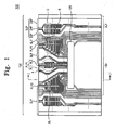
- FIG 1 is a top plan view of an exemplary embodiment of a tape carrier package (TCP) 100 in accordance with the present invention
- FIG 2 is a partial cross-sectional view of the exemplary TCP of FIG. 1 , as seen along the lines of the section I-I' taken therein.
- TCP tape carrier package
- the exemplary TCP 100 includes a base film 110, a semiconductor chip 120, a conductive input interconnection pattern 130, and a conductive output interconnection pattern 140.
- the base film 110 comprises an insulating material, such as polyimide.
- the semiconductor chip 120 is mounted on the base film 110, and includes transistors that use a first signal input from an external source and output a second signal in response thereto.
- the first signal drives the semiconductor chip 120, and includes an input power signal that provides the power required to drive the semiconductor chip 120, and a chip control signal that controls the operation of the semiconductor chip 120.
- the second signal output from the semiconductor chip 120 drives an external destination device connected to the output interconnection 140.
- the second signal may also include predetermined data signals.
- the bottom surface of the semiconductor chip 120 is provided with a plurality of input bumps 121 and a plurality of output bumps 122.
- the input bumps 121 are electrically connected to the input interconnection 130
- the output bumps 122 are electrically connected to the output interconnection 140.
- the input interconnection 130 is formed on the bottom surface of the base film 110, and is electrically connected to an external input device (not illustrated) so as to receive the first signal therefrom.
- the input interconnection 130 includes power interconnections PLP 1 and PLP2 that transmit the input power signal, and an input signal interconnection SLP that transmits the chip control signal.
- Each of the power interconnections PLP1 and PLP2 includes a plurality of power lines
- the input signal interconnection SLP includes a plurality of input signal lines.
- Each of the power lines and input signal lines have respective first end portions, each of which is formed with a first input pad IIP that receives the first signal from the external input source, and respective second end portions disposed opposite to the first end portions, each of which is formed with a second output pad IOP that outputs the first signal to the chip 120.
- Each of the first input pads IIP is formed at a first end portion of the base film 110, and is electrically connected to the external input device, and each of the first output pads IOP is electrically connected to a respective one or more of the input bumps 121 of the semiconductor chip 120.
- FIG 3 is an enlarged detail plan view of the region 'A' of the exemplary TCP of FIG 1
- FIG. 4 is an enlarged detail plan view of the region 'B' thereof.
- the power interconnections PLP1 and PLP2 are positioned adjacent to the input signal interconnection SLP.
- the power interconnection which is formed at the center of the TCP and crosses the base film 110 in a length direction of the power lines, is referred to herein as a first power connection PLP1.
- the power interconnections that are positioned on opposite sides of the first power interconnection PLP 1 are referred to herein as second and third power interconnections PLP2 and PLP3, respectively.
- the input signal lines are interspersed between the first power interconnection PLP 1 and the second and third power interconnections PLP2 and PLP3.
- the first power interconnection PLP 1 includes first and second power lines PL1 and PL2.
- the first and second power lines PL1 and PL2 are disposed adjacent to and spaced apart from each other by a predetermined distance.
- the first and second power lines PL1 and PL2 are bent, i.e., include alternating bends that extend in a widthwise direction of the power lines, so as to form a "serpentine" configuration or structure.
- the first and second power lines PL1 and PL2 can include respective bends that extend in the same direction as each other, or as illustrated in FIG 3 , respective bends that extend in opposite directions from each other.
- the first and second power lines PL1 and PL2 each forms a serpentine structure
- the first and second power lines PL1 and PL2 have respective lengths that are greater, and which can be more easily adjusted, than power lines that are relatively straight, i.e., which do not incorporate such a serpentine structure.
- the serpentine structures of the first and second power lines PL 1 and PL2 enable the input impedance of the semiconductor chip 110 to more exactly match the output impedance of the external input device.
- the resistance values of the first and second power lines PL1 and PL2 can be made to vary in accordance with the respective lengths thereof. Accordingly, the respective lengths of the first and second power lines PL1 and PL2 can be adjusted by taking into account the respective resistance values of the external input device and the semiconductor chip 110. By doing so, the impedance matching among the first and second power lines PL 1 and PL2, the external input device, and the semiconductor chip 110 can be optimized.
- the second power interconnection PLP2 and the third power interconnection PLP3 have the same structures, but are disposed symmetrically with respect to each other about a longitudinal line passing through about the middle of the semiconductor chip 120. Accordingly, the structure of the second power interconnection PLP2 on the right side of the line is described in detail below by way of example.
- the second power interconnection PLP2 includes third, fourth, fifth, and sixth power lines PL3, PL4, PL5, and PL6.
- the third, fourth, fifth, and sixth power lines PL3, PL4, PL5, and PL6 are arranged sequentially, and each is partially bent in a widthwise direction so as to incorporate a serpentine structure, as described above.
- the third and fourth power lines PL3 and PL4 can incorporate respective bends that extend in the same direction as each other, as illustrated in FIG 4 , or in another possible embodiment (not illustrated), that extend in opposite directions from each other. Additionally, as illustrated in FIG. 4 , the lengths of the longitudinally extending portions of the third and fourth power lines PL3 and PL4 may be the same as or may differ from the lengths of the laterally extending portions thereof.
- the fifth and sixth power lines PL5 and PL6 can also have respective bends that extend in the same or in opposite directions, as above, and further, can be bent in the same or in opposite directions relative to the third and fourth power lines PL3 and PL4. Also, as described above, the lengths of the longitudinally extending portions of the fifth and sixth power lines PL5 and PL6 may be the same as or may differ from the lengths of the laterally extending portions thereof.
- each of the third, fourth, fifth, and sixth power lines PL3, PL4, PL5, and PL6 incorporates a serpentine structure, their respective lengths are both greater, and can be more easily adjusted, than lines that do incorporate such serpentine structures. Accordingly, when impedance matching is implemented among the third, fourth, fifth, and sixth power lines PL3, PL4, PL5, and PL6, the external input device, and the semiconductor chip 110, the lengths of the third, fourth, fifth, and sixth power lines PL3, PL4, PL5, and PL6 can be adjusted by taking into account the resistance values of the external input device and the semiconductor chip 110.
- the impedance matching among the third, fourth, fifth, and sixth power lines PL3, PL4, PL5, and PL6, the external input device, and the semiconductor chip 110 can be optimized, and as a result, electromagnetic waves from the third; fourth, fifth, and sixth power lines PL3, PL4, PL5, and PL6 are thereby suppressed.
- This prevents the creation of electromagnetic noise in the input power signals, the disconnection of any of the third, fourth, fifth and sixth power lines PL3, PL4, PL5, and PL6, and the occurrence of damage to the semiconductor chip 110.
- all of the power lines of the first, second, and third power interconnections PLP1, PLP2, and PLP3 have serpentine structures, in other possible embodiments, only some of the power lines may incorporate a serpentine structure, depending on the size of the base film 110 and the number of lines of the input interconnection 130.
- the TCP 100 functions to suppress electromagnetic waves generated from the first, second, and third power interconnections PLP1, PLP2, and PLP3.
- the serpentine structures of the lines function to suppress electromagnetic waves in the TCP 100. Accordingly, the exemplary TCP 100 prevents the creation of noise, distortion of signals, damage to the semiconductor chip 120 and disconnection of the input interconnection 130 caused by electromagnetic waves, so that product yields are thereby improved.
- the signal lines of the input signal interconnection SLP transmit the chip control signal received from the external input device to the semiconductor chip 120.
- each of the input signal lines SL does not incorporate a serpentine structure. The reason for this is that, if the input signal line SL were to incorporate a serpentine structure, the control signal might be distorted thereby. Accordingly, the input signal lines SL are preferably made relatively straight, i.e. , with few, if any bends therein.
- the input interconnection 130 also includes auxiliary, "dummy" interconnections DLP, which respectively receive dummy power signals and dummy control signals from the external input device and output the dummy power signal and control signals to the external output device electrically connected to the output interconnection 140.
- the dummy power signals drive respective drivers that are connected to the external output device, and the dummy control signals control the operation of the drivers.
- the dummy interconnection DLP is not electrically connected to the semiconductor chip 120, but instead, bypasses the chip and thus serves as a pass-through of the dummy power and control signals from the external input device to the drivers on the external output device.
- a dummy interconnection DLP is shown disposed on both sides of an area corresponding to the first, second, and third power interconnections PLP1, PLP2, and PLP3 and the input signal interconnection SLP, in some possible embodiments, only one dummy interconnection DLP may be present on one or the other side thereof.
- the dummy interconnection DLP extends from a first end portion of the base film 110 to a second end portion that faces the first end portion.
- the dummy interconnection DLP includes a dummy power interconnection DPP, which transmits the dummy power signal, and a dummy signal interconnection DSP that transmits the dummy control signal.
- FIG 5 is an enlarged detail plan view of the region 'C' of the exemplary TCP of FIG. 1 .
- the dummy power interconnection DPP includes two dummy power lines DPL1 and DPL2 that are spaced apart from each other. A portion of the length of each of the dummy power lines DPL1 and DPL2 is bent in a widthwise direction thereof so as to incorporate a serpentine structure.
- the dummy power lines DPL 1 and DPL2 can include respective bends that extend in the same direction as each other, or as illustrated in FIG 5C , that extend in opposite directions from each other.
- each of the power-signal-carrying dummy power lines DPL1 and DPL2 incorporates a serpentine structure, the respective lengths of the dummy power lines DPL1 and DPL2 are both longer, and are more easily adjusted, than lines having a relatively straight structure.
- the serpentine structure enables the impedance match between the dummy power interconnection DPP and the external device to be optimized. Consequently, electromagnetic waves from the dummy power interconnection DPP are suppressed, thereby preventing the occurrence of any noise, signal distortion and disconnection of the dummy interconnection DLP caused by such electromagnetic waves.
- the output interconnection 140 of the TCP 100 is formed on the bottom surface of the base film 110 to transmit the second signal outputs from the semiconductor chip 120 to the external output device.
- the output interconnection 140 thus includes a plurality of output lines electrically connected between the semiconductor chip 120 and the external device.
- a first end portion of each of the output lines is formed with a second input pad OIP that receives a second signal from the semiconductor chip 120, and an opposite, second end portion of each of the output lines is formed with a second output pad OOP, which outputs the second signal.
- Each second input pad OIP is electrically connected to a respective one or more of the output bumps 122 of the semiconductor chip 120, and each second output pad OIP is electrically connected to an external destination device.
- An opening 111 is defined by removing a portion of the base film 110 on which the semiconductor chip 120 is mounted.
- a first output pad IOP of the input interconnection 130 and the second input pad OIP of the output interconnection 140 are exposed through the opening 111, and the bumps of the semiconductor chip 120 are electrically connected to respective ones of the first output pad IOP and the second input pad OIP within the opening 111.
- the TCP 100 includes a sealant 150 that fixes the semiconductor chip 120 to the base film 110 and a protection film 160 that protects the input interconnection 130 and the output interconnection 140.
- the sealant 150 surrounds the semiconductor chip 120 and seals the opening 111, so that the semiconductor chip 120 is fixed to the base film 110.
- the protection film 160 covers and protects the input and output interconnections 130 and 140. A portion of the protection film 160 corresponding to the opening 111 of the base film 110 is removed so that the first output pad IOP and the second input pad OIP are exposed.
- portions of the protection film 160 corresponding to the first and second end portions of the respective interconnections are also removed.
- FIG 6 is a graph of the intensity of an electromagnetic wave (EL) generated in the exemplary TCP of FIG 1 , plotted as a function of its frequency.
- the electromagnetic wave generated from the TCP 100 which is plotted relative to a criterion line (CL) corresponding to a maximum acceptable level of noise level, is situated below that maximum level by at least about 5SdB. That is, since the serpentine structures of the input interconnection 130 function to suppresses electromagnetic waves, electromagnetic waves are rarely generated from the TCP 100, and as a result, the first signal is not distorted due to electromagnetic noise.
- CL criterion line
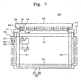
- FIG 7 is a plan view of an exemplary embodiment of an LCD 500 in accordance with the present invention.
- the exemplary display apparatus 500 includes a plurality of data TCPs 100, a plurality of gate TCPs 200, a liquid crystal display panel 300, and a printed circuit board 400.
- the liquid crystal display panel 300 includes an array substrate 310, an opposed substrate 320 facing the array substrate 320, and a liquid crystal layer (not illustrated) interposed between the array substrate 310 and the opposed substrate 3 20.
- the array substrate 310 includes first to Nth gate lines GL1 to GLn, first to Mth data lines DL1 to DLm, and a plurality of pixels 313.
- the first to Nth gate lines GL1 to GLn extend in one direction, and transmit respective gate signals corresponding to an image.
- the first to Mth data lines DL1 to DLm extend in a second direction orthogonal to the first direction so as to cross the first to Nth gate lines GL1 to GLn, but are insulated therefrom, and transmit respective data signals corresponding to the image.
- the pixels 313 are defined by intersections of the first to Nth gate lines GL1 to GLn and the first to Mth data lines DL1 to DLm, and each pixel 313 is a basic element of the image formed by the display panel 300.
- Each pixel 313 includes a thin film transistor 311, which switches a pixel voltage corresponding to the image, and a pixel electrode 312, which outputs the pixel voltage.
- the thin film transistor 311 is electrically connected to an associated gate line and an associated data line, and the pixel electrode 312 is electrically connected to a drain electrode of the associated thin film transistor 311.
- each data TCP 100 has the same elements as those of the TCP illustrated in FIG 1 and described above, the elements thereof that are the same as those of the embodiment of FIG 1 are referred to by the same reference numbers, and further detailed description of these elements is omitted for brevity. Also, for convenience of explanation, the semiconductor chips 120 respectively mounted on the data TCPs 100 are referred to as data driving chips.
- the input interconnection 130 of each data TCP 100 is electrically connected to the printed circuit board 400, and the output interconnection 140 of each data TCP 100 is electrically connected to a corresponding group of the first to Mth data lines DL1 to DLm of the array substrate 310.
- the input interconnection 130 receives a data power signal, which drives the data driving chip 120, and a data control signal, which corresponds to the image, from the printed circuit board 400 so as to provide the data power signal and the data control signal to the data driving chip 120.
- the power interconnections PLP1, PLP2, and PLP3 that transmit the data power signal have serpentine structures, the length of the input interconnection 130 can be easily adjusted, and is longer than a power interconnection having a conventionally straight structure. Accordingly, since the lengths of the power lines of the input interconnection 130 can be adjusted to achieve impedance matching relative to the printed circuit board 400, the electromagnetic waves can be suppressed and distortion of data control signals caused by noise can be prevented.
- the output interconnections 140 of the data TCPs 100 provide a data control signal output from the data driving chips 120 to the first to Mth data lines DL1 to DLm of the panel 300.
- the input interconnection 130 further includes a dummy interconnection DLP that transmits a gate power signal that drives the gate TCPs 200, and a gate control signal that controls the gate TCPs 200.
- the dummy interconnections DLP include a dummy power interconnection DPP, which transmits the gate power signals, and a dummy signal interconnection DSP, which transmits the gate control signals.
- the dummy power interconnections DPP and the dummy signal interconnections DSP are electrically connected to the array substrate 310.
- the array substrate 310 further includes link interconnections LL1 and LL2 which are electrically connected to respective dummy power and signal interconnections DPP and DSP so as to receive the gate power signal and the gate control signal.
- Each of the link interconnections LL 1 and LL2 is electrically connected to respective ones of the gate TCPs 210 to provide the gate power signal and the gate control signal, which are output from the respective dummy interconnections DLP, to the gate TCPs 200 respectively connected thereto.
- the gate TCPs 200 receive the gate power signal and the gate control signal through the data TCPs 100 and the respective link interconnections LL1 and LL2 of the array substrate 310.
- the gate TCPs 200 may be electrically connected to an additional gate printed circuit board (not illustrated), which outputs the gate power and control signals, and receive the gate and power signals exclusively from the gate printed circuit board.
- the data TCPs 100 and the array substrate 310 need not include the dummy interconnection DLP and the link interconnections LL1 and LL2.
- the gate TCPs 200 output the gate signal and provide the gate signal to the array substrate 310.
- the particular exemplary embodiment of FIG 7 is illustrated as having three gate TCPs 200 disposed on opposite side end portions of the array substrate 310, with the pixels 313 interposed therebetween, in another possible embodiment (not illustrated), the gate TCPs 200 can also be provided along only one side end portion of the array substrate 310.
- each gate TCP 200 has the same elements as those of the TCP illustrated in FIG. 1 and described above, the elements thereof that are the same as those of the embodiment of FIG 1 are referred to by the similar reference numbers, and further detailed description of these elements is omitted for brevity. Also, for convenience of explanation, the semiconductor chips 220 mounted on the gate TCPs 200 are referred to as gate driving chips.
- each gate TCP 200 is electrically connected to respective ones of the link interconnections LL 1 and LL2 to provide the gate power and driving signals to the corresponding gate driving chips 210.
- the power interconnection of each input interconnection 230 of the gate TCP 200 which transmits the gate power signals, incorporates a serpentine structure identical to that of the input interconnection 130 of the data TCPs 200. Accordingly, the length of the power line of the power interconnection of the gate TCP 200 that transmits the gate power signal can be easily adjusted, and is greater than the length of a power line having a relatively straight structure.
- the length of the power line of the gate TCP 200 can be adjusted so as to optimized the impedance matching relative to an external destination or input device, such as the array substrate 310 or the gate printed circuit board described above, electromagnetic waves in the gate TCPs 200 are suppressed, thereby preventing the distortion of the gate control signals caused by electromagnetic noise.
- Each gate driving chip 210 outputs gate signals in response to the gate power signal and the gate driving signal.
- the output interconnection 230 of the gate TCP 200 receives the gate signal from the gate driving chip 210, and is electrically connected to a corresponding group of the first to Nth gate lines GL1 to GLn of the array substrate 310 so as to controllably output the gate signals to that group of gate lines.
- the printed circuit board 400 is electrically connected to the data TCPs 100 to provide both the data and the gate power and control signals to the data TCPs 100, and the data TCPs 100 in turn provide the gate power and control signals to the gate TCPs 200 via the link interconnections LL1 and LL2.
- the power lines of the data and gate TCPs that transmit power input from an external source are provided with a serpentine structure, which increases the respective lengths of the power lines and enables them to be more easily adjusted than those of relatively straight power lines. Since the lengths of the power lines can be easily adjusted as described above, the TCPs enhance the ability to match the impedance between the power lines and an external input device providing power, and thereby suppress electromagnetic waves in the power lines. Accordingly, the TCPs prevent the creation of noise, distortion of signals, damage to the semiconductor chips thereon, and disconnection of the input interconnections thereof, all of which can be caused by the presence of electromagnetic waves, so that product yields are thereby improved.
Applications Claiming Priority (1)
| Application Number | Priority Date | Filing Date | Title |
|---|---|---|---|
| KR1020060088713A KR101352344B1 (ko) | 2006-09-13 | 2006-09-13 | 신호전송 부재 및 이를 갖는 표시장치 |
Publications (3)
| Publication Number | Publication Date |
|---|---|
| EP1901593A2 EP1901593A2 (en) | 2008-03-19 |
| EP1901593A3 EP1901593A3 (en) | 2009-07-29 |
| EP1901593B1 true EP1901593B1 (en) | 2012-03-07 |
Family
ID=38941850
Family Applications (1)
| Application Number | Title | Priority Date | Filing Date |
|---|---|---|---|
| EP07016073A Active EP1901593B1 (en) | 2006-09-13 | 2007-08-16 | LCD signal transfer members |
Country Status (5)
| Country | Link |
|---|---|
| US (1) | US7974103B2 (ko) |
| EP (1) | EP1901593B1 (ko) |
| JP (1) | JP5156259B2 (ko) |
| KR (1) | KR101352344B1 (ko) |
| CN (1) | CN101144921B (ko) |
Families Citing this family (32)
| Publication number | Priority date | Publication date | Assignee | Title |
|---|---|---|---|---|
| US7426780B2 (en) * | 2004-11-10 | 2008-09-23 | Enpirion, Inc. | Method of manufacturing a power module |
| US8701272B2 (en) | 2005-10-05 | 2014-04-22 | Enpirion, Inc. | Method of forming a power module with a magnetic device having a conductive clip |
| US8631560B2 (en) | 2005-10-05 | 2014-01-21 | Enpirion, Inc. | Method of forming a magnetic device having a conductive clip |
| US8139362B2 (en) | 2005-10-05 | 2012-03-20 | Enpirion, Inc. | Power module with a magnetic device having a conductive clip |
| US7688172B2 (en) | 2005-10-05 | 2010-03-30 | Enpirion, Inc. | Magnetic device having a conductive clip |
| US7920042B2 (en) | 2007-09-10 | 2011-04-05 | Enpirion, Inc. | Micromagnetic device and method of forming the same |
| US8133529B2 (en) * | 2007-09-10 | 2012-03-13 | Enpirion, Inc. | Method of forming a micromagnetic device |
| US8692532B2 (en) | 2008-04-16 | 2014-04-08 | Enpirion, Inc. | Power converter with controller operable in selected modes of operation |
| US8686698B2 (en) | 2008-04-16 | 2014-04-01 | Enpirion, Inc. | Power converter with controller operable in selected modes of operation |
| US8541991B2 (en) | 2008-04-16 | 2013-09-24 | Enpirion, Inc. | Power converter with controller operable in selected modes of operation |
| US9246390B2 (en) | 2008-04-16 | 2016-01-26 | Enpirion, Inc. | Power converter with controller operable in selected modes of operation |
| KR101460981B1 (ko) * | 2008-05-21 | 2014-11-14 | 삼성전자주식회사 | 전자파 간섭 차단 구조물, 및 이를 갖는 웨이퍼 레벨패키지 및 인쇄회로기판 |
| US8339802B2 (en) * | 2008-10-02 | 2012-12-25 | Enpirion, Inc. | Module having a stacked magnetic device and semiconductor device and method of forming the same |
| US8266793B2 (en) * | 2008-10-02 | 2012-09-18 | Enpirion, Inc. | Module having a stacked magnetic device and semiconductor device and method of forming the same |
| US9054086B2 (en) | 2008-10-02 | 2015-06-09 | Enpirion, Inc. | Module having a stacked passive element and method of forming the same |
| US8153473B2 (en) | 2008-10-02 | 2012-04-10 | Empirion, Inc. | Module having a stacked passive element and method of forming the same |
| US9548714B2 (en) | 2008-12-29 | 2017-01-17 | Altera Corporation | Power converter with a dynamically configurable controller and output filter |
| US8698463B2 (en) | 2008-12-29 | 2014-04-15 | Enpirion, Inc. | Power converter with a dynamically configurable controller based on a power conversion mode |
| US8791476B2 (en) | 2009-09-11 | 2014-07-29 | Sharp Kabushiki Kaisha | Active matrix substrate having a meander structure |
| KR101658141B1 (ko) * | 2009-12-01 | 2016-10-04 | 엘지디스플레이 주식회사 | 테이프 캐리어 패키지 및 액정표시장치 |
| JP5452290B2 (ja) * | 2010-03-05 | 2014-03-26 | ラピスセミコンダクタ株式会社 | 表示パネル |
| US8867295B2 (en) | 2010-12-17 | 2014-10-21 | Enpirion, Inc. | Power converter for a memory module |
| KR102026927B1 (ko) * | 2012-12-24 | 2019-10-01 | 엘지디스플레이 주식회사 | 구동부를 포함하는 표시장치 |
| KR102096038B1 (ko) | 2013-07-16 | 2020-04-02 | 삼성디스플레이 주식회사 | 전원 전달 배선을 포함하는 백라이트 유닛 |
| CN104349578A (zh) * | 2013-08-09 | 2015-02-11 | 福州高意通讯有限公司 | 一种多路传输的高频电路板 |
| KR102223125B1 (ko) | 2014-03-27 | 2021-03-05 | 삼성디스플레이 주식회사 | 데이터 구동부 및 이를 구비한 표시 장치 |
| US9444165B2 (en) | 2014-09-16 | 2016-09-13 | Via Technologies, Inc. | Pin arrangement and electronic assembly |
| KR101892689B1 (ko) * | 2014-10-14 | 2018-08-28 | 삼성전기주식회사 | 칩 전자부품 및 칩 전자부품의 실장 기판 |
| US9509217B2 (en) | 2015-04-20 | 2016-11-29 | Altera Corporation | Asymmetric power flow controller for a power converter and method of operating the same |
| KR101777716B1 (ko) * | 2016-08-04 | 2017-09-18 | 자화전자(주) | 회로기판 및 이를 포함하는 진동 발생장치 |
| US11095045B2 (en) | 2017-03-30 | 2021-08-17 | Intel Corporation | Slow wave structure for millimeter wave antennas |
| KR20200116582A (ko) * | 2019-04-01 | 2020-10-13 | 삼성디스플레이 주식회사 | 표시 장치, 포토 마스크 및 표시 장치의 제조 방법 |
Family Cites Families (39)
| Publication number | Priority date | Publication date | Assignee | Title |
|---|---|---|---|---|
| US4785135A (en) * | 1987-07-13 | 1988-11-15 | International Business Machines Corporation | De-coupled printed circuits |
| KR100370698B1 (ko) * | 1992-09-08 | 2003-03-31 | 세이코 엡슨 가부시키가이샤 | 액정표시장치 |
| US6765561B1 (en) * | 1992-10-21 | 2004-07-20 | Ray A. Stoller | Display device having integrated circuit chips thereon |
| JP3223647B2 (ja) * | 1993-07-08 | 2001-10-29 | 株式会社デンソー | 半導体集積回路装置 |
| JPH0710980U (ja) * | 1993-07-12 | 1995-02-14 | 株式会社船井電機研究所 | 多層プリント配線板 |
| TW275684B (ko) * | 1994-07-08 | 1996-05-11 | Hitachi Seisakusyo Kk | |
| KR100209863B1 (ko) * | 1995-01-13 | 1999-07-15 | 야스카와 히데아키 | 반도체 장치 테이프 캐리어 패키지 및 디스플레이 패널 모듈 |
| JP3593392B2 (ja) * | 1995-09-27 | 2004-11-24 | 株式会社東芝 | 液晶表示装置 |
| US6054975A (en) * | 1996-08-01 | 2000-04-25 | Hitachi, Ltd. | Liquid crystal display device having tape carrier packages |
| JPH10340070A (ja) * | 1997-06-09 | 1998-12-22 | Hitachi Ltd | 液晶表示装置 |
| JP3762568B2 (ja) * | 1998-08-18 | 2006-04-05 | 日本碍子株式会社 | ディスプレイの駆動装置及びディスプレイの駆動方法 |
| US6806862B1 (en) * | 1998-10-27 | 2004-10-19 | Fujitsu Display Technologies Corporation | Liquid crystal display device |
| KR100304261B1 (ko) * | 1999-04-16 | 2001-09-26 | 윤종용 | 테이프 캐리어 패키지, 그를 포함한 액정표시패널 어셈블리,그를 채용한 액정표시장치 및 이들의 조립 방법 |
| JP3681580B2 (ja) * | 1999-07-09 | 2005-08-10 | 株式会社日立製作所 | 液晶表示装置 |
| JP3267274B2 (ja) * | 1999-08-13 | 2002-03-18 | 日本電気株式会社 | 多層プリント基板 |
| TW527513B (en) * | 2000-03-06 | 2003-04-11 | Hitachi Ltd | Liquid crystal display device and manufacturing method thereof |
| JP2002009244A (ja) * | 2000-06-21 | 2002-01-11 | Hitachi Ltd | 半導体集積回路および半導体集積回路の設計方法 |
| KR100391843B1 (ko) * | 2001-03-26 | 2003-07-16 | 엘지.필립스 엘시디 주식회사 | 액정 표시 장치의 실장 방법 및 그 구조 |
| JP4439761B2 (ja) * | 2001-05-11 | 2010-03-24 | 株式会社半導体エネルギー研究所 | 液晶表示装置、電子機器 |
| JP2003140181A (ja) * | 2001-11-02 | 2003-05-14 | Nec Corp | 液晶表示装置 |
| KR100831303B1 (ko) * | 2001-12-26 | 2008-05-22 | 엘지디스플레이 주식회사 | 액정표시장치 |
| JP2003271108A (ja) * | 2002-03-18 | 2003-09-25 | Hitachi Ltd | 液晶表示装置 |
| WO2003104879A2 (en) * | 2002-06-01 | 2003-12-18 | Samsung Electronics Co., Ltd. | Shift register, liquid crystal display device having the shift register and method of driving scan lines using the same |
| TW584828B (en) * | 2002-06-25 | 2004-04-21 | Chi Mei Optoelectronics Corp | A driving circuit of a liquid crystal display device |
| US7071629B2 (en) * | 2003-03-31 | 2006-07-04 | Sony Corporation | Image display device incorporating driver circuits on active substrate and other methods to reduce interconnects |
| JP4443140B2 (ja) * | 2003-04-25 | 2010-03-31 | 株式会社 日立ディスプレイズ | 液晶表示装置 |
| KR100933447B1 (ko) * | 2003-06-24 | 2009-12-23 | 엘지디스플레이 주식회사 | 액정 표시 패널의 게이트 구동 방법 및 장치 |
| TW594177B (en) * | 2003-07-23 | 2004-06-21 | Hannstar Display Corp | Liquid crystal display panel for eliminating flicker |
| KR100977218B1 (ko) * | 2003-10-20 | 2010-08-23 | 엘지디스플레이 주식회사 | 라인 온 글래스형 액정 표시 장치 및 그 구동방법 |
| KR100983575B1 (ko) * | 2003-10-24 | 2010-09-27 | 엘지디스플레이 주식회사 | 액정 표시 장치 및 그의 구동방법 |
| JP4637512B2 (ja) * | 2003-11-13 | 2011-02-23 | ルネサスエレクトロニクス株式会社 | 半導体集積回路装置 |
| KR100996217B1 (ko) * | 2003-12-19 | 2010-11-24 | 삼성전자주식회사 | 표시장치 및 이의 구동방법 |
| JP4543725B2 (ja) * | 2004-03-30 | 2010-09-15 | セイコーエプソン株式会社 | 表示装置 |
| JP3857278B2 (ja) * | 2004-04-06 | 2006-12-13 | Smk株式会社 | タッチパネル入力装置 |
| JP4304134B2 (ja) * | 2004-08-03 | 2009-07-29 | シャープ株式会社 | 入力用配線フィルムおよびこれを備えた表示装置 |
| US20060044828A1 (en) * | 2004-09-02 | 2006-03-02 | Jae-Kwang Kim | Display device, driving device of display device, and driving device of light source for display device |
| KR20060060969A (ko) * | 2004-12-01 | 2006-06-07 | 디스플레이칩스 주식회사 | 엘시디 구동용 디바이스와, 이를 결합하기 위한 엘시디패널의 도전패턴 |
| KR20060080756A (ko) * | 2005-01-06 | 2006-07-11 | 삼성전자주식회사 | 신호전송필름, 이를 갖는 표시장치 및 이의 제조 방법 |
| KR100723490B1 (ko) * | 2005-07-12 | 2007-06-04 | 삼성전자주식회사 | 전자파 방해가 개선된 패턴을 구비한 테이프 배선기판 |
-
2006
- 2006-09-13 KR KR1020060088713A patent/KR101352344B1/ko active IP Right Grant
-
2007
- 2007-04-20 JP JP2007111581A patent/JP5156259B2/ja active Active
- 2007-08-13 US US11/893,043 patent/US7974103B2/en active Active
- 2007-08-16 EP EP07016073A patent/EP1901593B1/en active Active
- 2007-08-29 CN CN2007101425598A patent/CN101144921B/zh active Active
Also Published As
| Publication number | Publication date |
|---|---|
| US7974103B2 (en) | 2011-07-05 |
| KR101352344B1 (ko) | 2014-01-15 |
| EP1901593A3 (en) | 2009-07-29 |
| CN101144921A (zh) | 2008-03-19 |
| KR20080024401A (ko) | 2008-03-18 |
| CN101144921B (zh) | 2011-05-11 |
| US20080062666A1 (en) | 2008-03-13 |
| EP1901593A2 (en) | 2008-03-19 |
| JP2008072084A (ja) | 2008-03-27 |
| JP5156259B2 (ja) | 2013-03-06 |
Similar Documents
| Publication | Publication Date | Title |
|---|---|---|
| EP1901593B1 (en) | LCD signal transfer members | |
| US5737053A (en) | Wire substrate having branch lines perpendicular to the main lines in which the branch lines connect to driving circuits on a display device | |
| US9001300B2 (en) | Liquid crystal display | |
| JP3539555B2 (ja) | 液晶表示装置 | |
| US8502275B2 (en) | Thin film transistor array panel for a liquid crystal display | |
| US7459779B2 (en) | Pad arrangement of driver IC chip for LCD and related circuit pattern structure of TAB package | |
| KR100341552B1 (ko) | 액정 표시 장치 | |
| US6624868B1 (en) | Chip-on-glass (COG) structure liquid crystal display (LCD) | |
| KR20120054683A (ko) | 네로우 베젤 타입 어레이 기판 및 이를 구비한 액정표시장치 | |
| KR101621559B1 (ko) | 액정표시장치 | |
| US7133106B2 (en) | Liquid crystal display device with flexible printed circuit board | |
| KR100687535B1 (ko) | 액정표시장치의 구동장치 | |
| CN114879421B (zh) | 一种驱动电路及显示装置 | |
| US11579497B2 (en) | Substrate for display device and display device | |
| US8681281B2 (en) | Grounding structure for display device | |
| JP2006106132A (ja) | 表示駆動回路および表示装置 | |
| CN115047681A (zh) | 阵列基板、显示面板和制作方法 | |
| KR20040098869A (ko) | 액정표시장치의 패드구조 | |
| KR20080074586A (ko) | 디스플레이 구동 칩에 연결된 배선 기판을 구비하는디스플레이 장치 | |
| JPH05173162A (ja) | 液晶表示装置 | |
| KR20060081217A (ko) | 액정표시장치 |
Legal Events
| Date | Code | Title | Description |
|---|---|---|---|
| PUAI | Public reference made under article 153(3) epc to a published international application that has entered the european phase |
Free format text: ORIGINAL CODE: 0009012 |
|
| AK | Designated contracting states |
Kind code of ref document: A2 Designated state(s): AT BE BG CH CY CZ DE DK EE ES FI FR GB GR HU IE IS IT LI LT LU LV MC MT NL PL PT RO SE SI SK TR |
|
| AX | Request for extension of the european patent |
Extension state: AL BA HR MK YU |
|
| PUAL | Search report despatched |
Free format text: ORIGINAL CODE: 0009013 |
|
| AK | Designated contracting states |
Kind code of ref document: A3 Designated state(s): AT BE BG CH CY CZ DE DK EE ES FI FR GB GR HU IE IS IT LI LT LU LV MC MT NL PL PT RO SE SI SK TR |
|
| AX | Request for extension of the european patent |
Extension state: AL BA HR MK RS |
|
| 17P | Request for examination filed |
Effective date: 20100114 |
|
| 17Q | First examination report despatched |
Effective date: 20100212 |
|
| AKX | Designation fees paid |
Designated state(s): DE FR GB IT NL |
|
| GRAP | Despatch of communication of intention to grant a patent |
Free format text: ORIGINAL CODE: EPIDOSNIGR1 |
|
| GRAS | Grant fee paid |
Free format text: ORIGINAL CODE: EPIDOSNIGR3 |
|
| GRAA | (expected) grant |
Free format text: ORIGINAL CODE: 0009210 |
|
| AK | Designated contracting states |
Kind code of ref document: B1 Designated state(s): DE FR GB IT NL |
|
| REG | Reference to a national code |
Ref country code: GB Ref legal event code: FG4D |
|
| REG | Reference to a national code |
Ref country code: NL Ref legal event code: T3 |
|
| REG | Reference to a national code |
Ref country code: DE Ref legal event code: R096 Ref document number: 602007021092 Country of ref document: DE Effective date: 20120503 |
|
| RAP2 | Party data changed (patent owner data changed or rights of a patent transferred) |
Owner name: SAMSUNG ELECTRONICS CO., LTD. |
|
| REG | Reference to a national code |
Ref country code: NL Ref legal event code: SD Effective date: 20121017 |
|
| RAP2 | Party data changed (patent owner data changed or rights of a patent transferred) |
Owner name: SAMSUNG DISPLAY CO., LTD. |
|
| PLBE | No opposition filed within time limit |
Free format text: ORIGINAL CODE: 0009261 |
|
| STAA | Information on the status of an ep patent application or granted ep patent |
Free format text: STATUS: NO OPPOSITION FILED WITHIN TIME LIMIT |
|
| 26N | No opposition filed |
Effective date: 20121210 |
|
| REG | Reference to a national code |
Ref country code: FR Ref legal event code: TP Owner name: SAMSUNG DISPLAY CO. LTD, KR Effective date: 20130226 |
|
| REG | Reference to a national code |
Ref country code: GB Ref legal event code: 732E Free format text: REGISTERED BETWEEN 20130307 AND 20130313 |
|
| REG | Reference to a national code |
Ref country code: DE Ref legal event code: R097 Ref document number: 602007021092 Country of ref document: DE Effective date: 20121210 |
|
| REG | Reference to a national code |
Ref country code: DE Ref legal event code: R082 Ref document number: 602007021092 Country of ref document: DE Representative=s name: DR. WEITZEL & PARTNER, DE |
|
| REG | Reference to a national code |
Ref country code: DE Ref legal event code: R082 Ref document number: 602007021092 Country of ref document: DE Representative=s name: DR. WEITZEL & PARTNER PATENT- UND RECHTSANWAEL, DE Effective date: 20130422 Ref country code: DE Ref legal event code: R082 Ref document number: 602007021092 Country of ref document: DE Representative=s name: DR. WEITZEL & PARTNER, DE Effective date: 20130422 Ref country code: DE Ref legal event code: R081 Ref document number: 602007021092 Country of ref document: DE Owner name: SAMSUNG DISPLAY CO., LTD., YONGIN-CITY, KR Free format text: FORMER OWNER: SAMSUNG ELECTRONICS CO., LTD., SUWON-SI, GYEONGGI-DO, KR Effective date: 20130422 Ref country code: DE Ref legal event code: R081 Ref document number: 602007021092 Country of ref document: DE Owner name: SAMSUNG DISPLAY CO., LTD., KR Free format text: FORMER OWNER: SAMSUNG ELECTRONICS CO., LTD., SUWON-SI, KR Effective date: 20130422 |
|
| REG | Reference to a national code |
Ref country code: FR Ref legal event code: PLFP Year of fee payment: 10 |
|
| REG | Reference to a national code |
Ref country code: FR Ref legal event code: PLFP Year of fee payment: 11 |
|
| REG | Reference to a national code |
Ref country code: FR Ref legal event code: PLFP Year of fee payment: 12 |
|
| P01 | Opt-out of the competence of the unified patent court (upc) registered |
Effective date: 20230515 |
|
| PGFP | Annual fee paid to national office [announced via postgrant information from national office to epo] |
Ref country code: NL Payment date: 20230721 Year of fee payment: 17 |
|
| PGFP | Annual fee paid to national office [announced via postgrant information from national office to epo] |
Ref country code: IT Payment date: 20230724 Year of fee payment: 17 Ref country code: GB Payment date: 20230720 Year of fee payment: 17 |
|
| PGFP | Annual fee paid to national office [announced via postgrant information from national office to epo] |
Ref country code: FR Payment date: 20230725 Year of fee payment: 17 Ref country code: DE Payment date: 20230720 Year of fee payment: 17 |