JP5156259B2 - 表示装置 - Google Patents
表示装置 Download PDFInfo
- Publication number
- JP5156259B2 JP5156259B2 JP2007111581A JP2007111581A JP5156259B2 JP 5156259 B2 JP5156259 B2 JP 5156259B2 JP 2007111581 A JP2007111581 A JP 2007111581A JP 2007111581 A JP2007111581 A JP 2007111581A JP 5156259 B2 JP5156259 B2 JP 5156259B2
- Authority
- JP
- Japan
- Prior art keywords
- signal
- input
- semiconductor chip
- power supply
- lines
- Prior art date
- Legal status (The legal status is an assumption and is not a legal conclusion. Google has not performed a legal analysis and makes no representation as to the accuracy of the status listed.)
- Active
Links
- 239000004065 semiconductor Substances 0.000 claims description 74
- 230000008054 signal transmission Effects 0.000 claims description 17
- 238000009616 inductively coupled plasma Methods 0.000 description 48
- 235000010384 tocopherol Nutrition 0.000 description 48
- 235000019731 tricalcium phosphate Nutrition 0.000 description 48
- 239000010408 film Substances 0.000 description 43
- 239000000758 substrate Substances 0.000 description 24
- 101001126414 Homo sapiens Proteolipid protein 2 Proteins 0.000 description 20
- 101001129122 Mannheimia haemolytica Outer membrane lipoprotein 2 Proteins 0.000 description 20
- 101000642171 Odontomachus monticola U-poneritoxin(01)-Om2a Proteins 0.000 description 20
- 102100030486 Proteolipid protein 2 Human genes 0.000 description 20
- 101000982010 Homo sapiens Myelin proteolipid protein Proteins 0.000 description 15
- 101001129124 Mannheimia haemolytica Outer membrane lipoprotein 1 Proteins 0.000 description 15
- 102100026784 Myelin proteolipid protein Human genes 0.000 description 15
- 101000761187 Odontomachus monticola U-poneritoxin(01)-Om1a Proteins 0.000 description 15
- 239000004973 liquid crystal related substance Substances 0.000 description 12
- 101001129120 Mannheimia haemolytica Outer membrane lipoprotein 3 Proteins 0.000 description 11
- 101000606232 Odontomachus monticola U-poneritoxin(01)-Om3a Proteins 0.000 description 11
- 239000010409 thin film Substances 0.000 description 6
- 102100036966 Dipeptidyl aminopeptidase-like protein 6 Human genes 0.000 description 5
- 101000804935 Homo sapiens Dipeptidyl aminopeptidase-like protein 6 Proteins 0.000 description 5
- 230000001681 protective effect Effects 0.000 description 5
- 101000967820 Homo sapiens Inactive dipeptidyl peptidase 10 Proteins 0.000 description 4
- 102100040449 Inactive dipeptidyl peptidase 10 Human genes 0.000 description 4
- 238000000926 separation method Methods 0.000 description 4
- 239000000853 adhesive Substances 0.000 description 3
- 230000001070 adhesive effect Effects 0.000 description 3
- 101000872016 Campylobacter jejuni subsp. jejuni serotype O:23/36 (strain 81-176) Dynamin-like protein 2 Proteins 0.000 description 1
- 239000004642 Polyimide Substances 0.000 description 1
- 239000011810 insulating material Substances 0.000 description 1
- 230000003287 optical effect Effects 0.000 description 1
- 229920001721 polyimide Polymers 0.000 description 1
Images


Classifications
-
- H—ELECTRICITY
- H05—ELECTRIC TECHNIQUES NOT OTHERWISE PROVIDED FOR
- H05K—PRINTED CIRCUITS; CASINGS OR CONSTRUCTIONAL DETAILS OF ELECTRIC APPARATUS; MANUFACTURE OF ASSEMBLAGES OF ELECTRICAL COMPONENTS
- H05K1/00—Printed circuits
- H05K1/02—Details
- H05K1/0213—Electrical arrangements not otherwise provided for
- H05K1/0216—Reduction of cross-talk, noise or electromagnetic interference
-
- G—PHYSICS
- G02—OPTICS
- G02F—OPTICAL DEVICES OR ARRANGEMENTS FOR THE CONTROL OF LIGHT BY MODIFICATION OF THE OPTICAL PROPERTIES OF THE MEDIA OF THE ELEMENTS INVOLVED THEREIN; NON-LINEAR OPTICS; FREQUENCY-CHANGING OF LIGHT; OPTICAL LOGIC ELEMENTS; OPTICAL ANALOGUE/DIGITAL CONVERTERS
- G02F1/00—Devices or arrangements for the control of the intensity, colour, phase, polarisation or direction of light arriving from an independent light source, e.g. switching, gating or modulating; Non-linear optics
- G02F1/01—Devices or arrangements for the control of the intensity, colour, phase, polarisation or direction of light arriving from an independent light source, e.g. switching, gating or modulating; Non-linear optics for the control of the intensity, phase, polarisation or colour
- G02F1/13—Devices or arrangements for the control of the intensity, colour, phase, polarisation or direction of light arriving from an independent light source, e.g. switching, gating or modulating; Non-linear optics for the control of the intensity, phase, polarisation or colour based on liquid crystals, e.g. single liquid crystal display cells
- G02F1/133—Constructional arrangements; Operation of liquid crystal cells; Circuit arrangements
- G02F1/136—Liquid crystal cells structurally associated with a semi-conducting layer or substrate, e.g. cells forming part of an integrated circuit
-
- G—PHYSICS
- G02—OPTICS
- G02F—OPTICAL DEVICES OR ARRANGEMENTS FOR THE CONTROL OF LIGHT BY MODIFICATION OF THE OPTICAL PROPERTIES OF THE MEDIA OF THE ELEMENTS INVOLVED THEREIN; NON-LINEAR OPTICS; FREQUENCY-CHANGING OF LIGHT; OPTICAL LOGIC ELEMENTS; OPTICAL ANALOGUE/DIGITAL CONVERTERS
- G02F1/00—Devices or arrangements for the control of the intensity, colour, phase, polarisation or direction of light arriving from an independent light source, e.g. switching, gating or modulating; Non-linear optics
- G02F1/01—Devices or arrangements for the control of the intensity, colour, phase, polarisation or direction of light arriving from an independent light source, e.g. switching, gating or modulating; Non-linear optics for the control of the intensity, phase, polarisation or colour
- G02F1/13—Devices or arrangements for the control of the intensity, colour, phase, polarisation or direction of light arriving from an independent light source, e.g. switching, gating or modulating; Non-linear optics for the control of the intensity, phase, polarisation or colour based on liquid crystals, e.g. single liquid crystal display cells
- G02F1/133—Constructional arrangements; Operation of liquid crystal cells; Circuit arrangements
- G02F1/1333—Constructional arrangements; Manufacturing methods
- G02F1/1345—Conductors connecting electrodes to cell terminals
- G02F1/13452—Conductors connecting driver circuitry and terminals of panels
-
- H—ELECTRICITY
- H05—ELECTRIC TECHNIQUES NOT OTHERWISE PROVIDED FOR
- H05K—PRINTED CIRCUITS; CASINGS OR CONSTRUCTIONAL DETAILS OF ELECTRIC APPARATUS; MANUFACTURE OF ASSEMBLAGES OF ELECTRICAL COMPONENTS
- H05K1/00—Printed circuits
- H05K1/02—Details
- H05K1/0213—Electrical arrangements not otherwise provided for
- H05K1/0237—High frequency adaptations
- H05K1/025—Impedance arrangements, e.g. impedance matching, reduction of parasitic impedance
-
- H—ELECTRICITY
- H05—ELECTRIC TECHNIQUES NOT OTHERWISE PROVIDED FOR
- H05K—PRINTED CIRCUITS; CASINGS OR CONSTRUCTIONAL DETAILS OF ELECTRIC APPARATUS; MANUFACTURE OF ASSEMBLAGES OF ELECTRICAL COMPONENTS
- H05K1/00—Printed circuits
- H05K1/18—Printed circuits structurally associated with non-printed electric components
- H05K1/189—Printed circuits structurally associated with non-printed electric components characterised by the use of a flexible or folded printed circuit
-
- H—ELECTRICITY
- H05—ELECTRIC TECHNIQUES NOT OTHERWISE PROVIDED FOR
- H05K—PRINTED CIRCUITS; CASINGS OR CONSTRUCTIONAL DETAILS OF ELECTRIC APPARATUS; MANUFACTURE OF ASSEMBLAGES OF ELECTRICAL COMPONENTS
- H05K2201/00—Indexing scheme relating to printed circuits covered by H05K1/00
- H05K2201/09—Shape and layout
- H05K2201/09209—Shape and layout details of conductors
- H05K2201/09218—Conductive traces
- H05K2201/09236—Parallel layout
-
- H—ELECTRICITY
- H05—ELECTRIC TECHNIQUES NOT OTHERWISE PROVIDED FOR
- H05K—PRINTED CIRCUITS; CASINGS OR CONSTRUCTIONAL DETAILS OF ELECTRIC APPARATUS; MANUFACTURE OF ASSEMBLAGES OF ELECTRICAL COMPONENTS
- H05K2201/00—Indexing scheme relating to printed circuits covered by H05K1/00
- H05K2201/09—Shape and layout
- H05K2201/09209—Shape and layout details of conductors
- H05K2201/09218—Conductive traces
- H05K2201/09263—Meander
-
- H—ELECTRICITY
- H05—ELECTRIC TECHNIQUES NOT OTHERWISE PROVIDED FOR
- H05K—PRINTED CIRCUITS; CASINGS OR CONSTRUCTIONAL DETAILS OF ELECTRIC APPARATUS; MANUFACTURE OF ASSEMBLAGES OF ELECTRICAL COMPONENTS
- H05K2201/00—Indexing scheme relating to printed circuits covered by H05K1/00
- H05K2201/09—Shape and layout
- H05K2201/09209—Shape and layout details of conductors
- H05K2201/09654—Shape and layout details of conductors covering at least two types of conductors provided for in H05K2201/09218 - H05K2201/095
- H05K2201/09781—Dummy conductors, i.e. not used for normal transport of current; Dummy electrodes of components
-
- H—ELECTRICITY
- H05—ELECTRIC TECHNIQUES NOT OTHERWISE PROVIDED FOR
- H05K—PRINTED CIRCUITS; CASINGS OR CONSTRUCTIONAL DETAILS OF ELECTRIC APPARATUS; MANUFACTURE OF ASSEMBLAGES OF ELECTRICAL COMPONENTS
- H05K2201/00—Indexing scheme relating to printed circuits covered by H05K1/00
- H05K2201/10—Details of components or other objects attached to or integrated in a printed circuit board
- H05K2201/10007—Types of components
- H05K2201/10128—Display
- H05K2201/10136—Liquid Crystal display [LCD]
-
- H—ELECTRICITY
- H05—ELECTRIC TECHNIQUES NOT OTHERWISE PROVIDED FOR
- H05K—PRINTED CIRCUITS; CASINGS OR CONSTRUCTIONAL DETAILS OF ELECTRIC APPARATUS; MANUFACTURE OF ASSEMBLAGES OF ELECTRICAL COMPONENTS
- H05K2201/00—Indexing scheme relating to printed circuits covered by H05K1/00
- H05K2201/10—Details of components or other objects attached to or integrated in a printed circuit board
- H05K2201/10613—Details of electrical connections of non-printed components, e.g. special leads
- H05K2201/10621—Components characterised by their electrical contacts
- H05K2201/10681—Tape Carrier Package [TCP]; Flexible sheet connector
Description
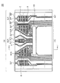
110 ベースフィルム
120 半導体チップ
130 入力配線部
140 出力配線部
150 接着部材
160 保護フィルム
Claims (9)
- 映像信号に対応して映像を表示する表示パネルと、
前記表示パネルの端部に付着し、前記映像信号を出力して前記表示パネルに供給する少なくとも1つの信号伝送部材とを含み、
前記信号伝送部材は、
ベースフィルムと、
前記ベースフィルムに実装され、前記映像に対応する入力信号を受信して前記映像信号を出力する半導体チップと、
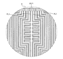
前記ベースフィルムに形成されて前記半導体チップと電気的に接続され、一部分が蛇行形状を有するように折れ曲がり、前記入力信号を前記半導体チップに供給する入力配線部と、
前記ベースフィルムに形成され、前記半導体チップ及び前記表示パネルと電気的に接続され、前記半導体チップから出力された前記映像信号を前記表示パネルに供給する出力配線部とを含み、
前記入力配線部は、
前記チップ電源信号を送り、同一の蛇行形状を有するように折れ曲がった複数の入力電源ラインと、
前記複数の入力電源ラインから離間し、繰り返しの折れ曲がり部分を有さない、前記制御信号を送る複数の入力信号ラインとを含み、
前記複数の入力電源ライン及び入力信号ラインはそれぞれ、左右対称に配置されていることを特徴とする表示装置。 - 前記入力信号は、
前記半導体チップを駆動するチップ電源信号と、
前記映像信号を生成するための制御信号とを含むことを特徴とする請求項1に記載の表示装置。 - 前記表示パネルは、前記出力配線部と電気的に接続されて前記映像信号を送る複数の映像信号ラインを含むことを特徴とする請求項1に記載の表示装置。
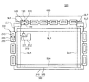
- 前記信号伝送部材と電気的に接続され、前記入力信号を出力して前記信号伝送部材に供給する印刷回路部をさらに含むことを特徴とする請求項3に記載の表示装置。
- 前記入力配線部は、前記印刷回路部からサブ電源信号を受信して前記表示パネルに供給する複数のダミー電源ラインをさらに含むことを特徴とする請求項4に記載の表示装置。
- 前記ダミー電源ラインのうちの少なくともいずれか1つは蛇行形状を有するように折れ曲がったことを特徴とする請求項5に記載の表示装置。
- 前記表示パネルは、前記ダミー電源ラインと電気的に接続され、前記ダミー電源ラインから出力された前記サブ電源信号を送る複数の接続ラインをさらに含むことを特徴とする請求項6に記載の表示装置。
- 前記信号伝送部材はテープキャリアパッケージであることを特徴とする請求項1に記載の表示装置。
- 映像を表示する表示パネルと、
前記表示パネルに付着した第1ベースフィルム、前記第1ベースフィルムに実装され、前記映像に対応する第1入力信号を受信してデータ信号を出力する第1半導体チップ、前記第1ベースフィルムに形成されて前記第1半導体チップと電気的に接続され、一部分が蛇行形状を有するように折れ曲がり、前記第1入力信号を前記第1半導体チップに供給する第1入力配線部、及び前記第1ベースフィルムに形成され、前記第1半導体チップ及び前記表示パネルと電気的に接続され、前記第1半導体チップから出力された前記データ信号を前記表示パネルに供給する第1出力配線部を含む少なくとも1つのデータテープキャリアパッケージと、
前記表示パネルに付着した第2ベースフィルム、前記第2ベースフィルムに実装され、前記映像に対応する第2入力信号を受信してゲート信号を出力する第2半導体チップ、前記第2ベースフィルムに形成されて前記第2半導体チップと電気的に接続され、前記第2入力信号を前記第2半導体チップに供給する第2入力配線部、及び前記第2ベースフィルムに形成され、前記第2半導体チップ及び前記表示パネルと電気的に接続され、前記第2半導体チップから出力された前記ゲート信号を前記表示パネルに供給する第2出力配線部を含む少なくとも1つのゲートテープキャリアパッケージとを含み、
前記第1入力配線部は、
前記チップ電源信号を送り、同一の蛇行形状を有するように折れ曲がった複数の第1入力電源ラインと、
前記複数の第1入力電源ラインから離間し、蛇行形状を有さない、前記制御信号を送る複数の入力信号ラインとを含み、
前記複数の第1入力電源ライン及び入力信号ラインはそれぞれ、左右対称に配置されており、
前記第2入力配線部は、
前記チップ電源信号を送り、同一の蛇行形状を有するように折れ曲がった複数の第2入力電源ラインと、
前記複数の第2入力電源ラインから離間し、蛇行形状を有さない、前記制御信号を送る複数の入力信号ラインとを含み、
前記複数の第2入力電源ライン及び入力信号ラインはそれぞれ、左右対称に配置されていることを特徴とする表示装置。
Applications Claiming Priority (2)
| Application Number | Priority Date | Filing Date | Title |
|---|---|---|---|
| KR10-2006-0088713 | 2006-09-13 | ||
| KR1020060088713A KR101352344B1 (ko) | 2006-09-13 | 2006-09-13 | 신호전송 부재 및 이를 갖는 표시장치 |
Publications (3)
| Publication Number | Publication Date |
|---|---|
| JP2008072084A JP2008072084A (ja) | 2008-03-27 |
| JP2008072084A5 JP2008072084A5 (ja) | 2010-04-22 |
| JP5156259B2 true JP5156259B2 (ja) | 2013-03-06 |
Family
ID=38941850
Family Applications (1)
| Application Number | Title | Priority Date | Filing Date |
|---|---|---|---|
| JP2007111581A Active JP5156259B2 (ja) | 2006-09-13 | 2007-04-20 | 表示装置 |
Country Status (5)
| Country | Link |
|---|---|
| US (1) | US7974103B2 (ja) |
| EP (1) | EP1901593B1 (ja) |
| JP (1) | JP5156259B2 (ja) |
| KR (1) | KR101352344B1 (ja) |
| CN (1) | CN101144921B (ja) |
Families Citing this family (32)
| Publication number | Priority date | Publication date | Assignee | Title |
|---|---|---|---|---|
| US7426780B2 (en) * | 2004-11-10 | 2008-09-23 | Enpirion, Inc. | Method of manufacturing a power module |
| US8139362B2 (en) | 2005-10-05 | 2012-03-20 | Enpirion, Inc. | Power module with a magnetic device having a conductive clip |
| US7688172B2 (en) | 2005-10-05 | 2010-03-30 | Enpirion, Inc. | Magnetic device having a conductive clip |
| US8701272B2 (en) | 2005-10-05 | 2014-04-22 | Enpirion, Inc. | Method of forming a power module with a magnetic device having a conductive clip |
| US8631560B2 (en) | 2005-10-05 | 2014-01-21 | Enpirion, Inc. | Method of forming a magnetic device having a conductive clip |
| US7920042B2 (en) | 2007-09-10 | 2011-04-05 | Enpirion, Inc. | Micromagnetic device and method of forming the same |
| US8133529B2 (en) * | 2007-09-10 | 2012-03-13 | Enpirion, Inc. | Method of forming a micromagnetic device |
| US8686698B2 (en) | 2008-04-16 | 2014-04-01 | Enpirion, Inc. | Power converter with controller operable in selected modes of operation |
| US9246390B2 (en) | 2008-04-16 | 2016-01-26 | Enpirion, Inc. | Power converter with controller operable in selected modes of operation |
| US8692532B2 (en) | 2008-04-16 | 2014-04-08 | Enpirion, Inc. | Power converter with controller operable in selected modes of operation |
| US8541991B2 (en) | 2008-04-16 | 2013-09-24 | Enpirion, Inc. | Power converter with controller operable in selected modes of operation |
| KR101460981B1 (ko) * | 2008-05-21 | 2014-11-14 | 삼성전자주식회사 | 전자파 간섭 차단 구조물, 및 이를 갖는 웨이퍼 레벨패키지 및 인쇄회로기판 |
| US8266793B2 (en) * | 2008-10-02 | 2012-09-18 | Enpirion, Inc. | Module having a stacked magnetic device and semiconductor device and method of forming the same |
| US8339802B2 (en) * | 2008-10-02 | 2012-12-25 | Enpirion, Inc. | Module having a stacked magnetic device and semiconductor device and method of forming the same |
| US8153473B2 (en) | 2008-10-02 | 2012-04-10 | Empirion, Inc. | Module having a stacked passive element and method of forming the same |
| US9054086B2 (en) | 2008-10-02 | 2015-06-09 | Enpirion, Inc. | Module having a stacked passive element and method of forming the same |
| US9548714B2 (en) | 2008-12-29 | 2017-01-17 | Altera Corporation | Power converter with a dynamically configurable controller and output filter |
| US8698463B2 (en) | 2008-12-29 | 2014-04-15 | Enpirion, Inc. | Power converter with a dynamically configurable controller based on a power conversion mode |
| JP5192080B2 (ja) * | 2009-09-11 | 2013-05-08 | シャープ株式会社 | アクティブマトリクス基板及び表示装置 |
| KR101658141B1 (ko) * | 2009-12-01 | 2016-10-04 | 엘지디스플레이 주식회사 | 테이프 캐리어 패키지 및 액정표시장치 |
| JP5452290B2 (ja) * | 2010-03-05 | 2014-03-26 | ラピスセミコンダクタ株式会社 | 表示パネル |
| US8867295B2 (en) | 2010-12-17 | 2014-10-21 | Enpirion, Inc. | Power converter for a memory module |
| KR102026927B1 (ko) * | 2012-12-24 | 2019-10-01 | 엘지디스플레이 주식회사 | 구동부를 포함하는 표시장치 |
| KR102096038B1 (ko) | 2013-07-16 | 2020-04-02 | 삼성디스플레이 주식회사 | 전원 전달 배선을 포함하는 백라이트 유닛 |
| CN104349578A (zh) * | 2013-08-09 | 2015-02-11 | 福州高意通讯有限公司 | 一种多路传输的高频电路板 |
| KR102223125B1 (ko) | 2014-03-27 | 2021-03-05 | 삼성디스플레이 주식회사 | 데이터 구동부 및 이를 구비한 표시 장치 |
| US9444165B2 (en) | 2014-09-16 | 2016-09-13 | Via Technologies, Inc. | Pin arrangement and electronic assembly |
| KR101892689B1 (ko) | 2014-10-14 | 2018-08-28 | 삼성전기주식회사 | 칩 전자부품 및 칩 전자부품의 실장 기판 |
| US9509217B2 (en) | 2015-04-20 | 2016-11-29 | Altera Corporation | Asymmetric power flow controller for a power converter and method of operating the same |
| KR101777716B1 (ko) * | 2016-08-04 | 2017-09-18 | 자화전자(주) | 회로기판 및 이를 포함하는 진동 발생장치 |
| WO2018182628A1 (en) | 2017-03-30 | 2018-10-04 | Intel Corporation | Slow wave structure for millimeter wave antennas |
| KR20200116582A (ko) * | 2019-04-01 | 2020-10-13 | 삼성디스플레이 주식회사 | 표시 장치, 포토 마스크 및 표시 장치의 제조 방법 |
Family Cites Families (39)
| Publication number | Priority date | Publication date | Assignee | Title |
|---|---|---|---|---|
| US4785135A (en) * | 1987-07-13 | 1988-11-15 | International Business Machines Corporation | De-coupled printed circuits |
| EP0587144B1 (en) * | 1992-09-08 | 1999-06-09 | Seiko Epson Corporation | Liquid crystal display apparatus, structure for mounting semiconductor device, method of mounting semiconductor device, electronic optical apparatus and electronic printing apparatus |
| US6765561B1 (en) * | 1992-10-21 | 2004-07-20 | Ray A. Stoller | Display device having integrated circuit chips thereon |
| JP3223647B2 (ja) * | 1993-07-08 | 2001-10-29 | 株式会社デンソー | 半導体集積回路装置 |
| JPH0710980U (ja) * | 1993-07-12 | 1995-02-14 | 株式会社船井電機研究所 | 多層プリント配線板 |
| TW275684B (ja) * | 1994-07-08 | 1996-05-11 | Hitachi Seisakusyo Kk | |
| WO1996021948A1 (fr) * | 1995-01-13 | 1996-07-18 | Seiko Epson Corporation | Dispositif semi-conducteur, support de bande et panneau d'affichage |
| JP3593392B2 (ja) * | 1995-09-27 | 2004-11-24 | 株式会社東芝 | 液晶表示装置 |
| KR100240818B1 (ko) * | 1996-08-01 | 2000-01-15 | 나시모토 류조 | 테이프캐리어패키지를 구비한 액정표시장치 |
| JPH10340070A (ja) * | 1997-06-09 | 1998-12-22 | Hitachi Ltd | 液晶表示装置 |
| JP3762568B2 (ja) * | 1998-08-18 | 2006-04-05 | 日本碍子株式会社 | ディスプレイの駆動装置及びディスプレイの駆動方法 |
| US6806862B1 (en) * | 1998-10-27 | 2004-10-19 | Fujitsu Display Technologies Corporation | Liquid crystal display device |
| KR100304261B1 (ko) * | 1999-04-16 | 2001-09-26 | 윤종용 | 테이프 캐리어 패키지, 그를 포함한 액정표시패널 어셈블리,그를 채용한 액정표시장치 및 이들의 조립 방법 |
| JP3681580B2 (ja) * | 1999-07-09 | 2005-08-10 | 株式会社日立製作所 | 液晶表示装置 |
| JP3267274B2 (ja) * | 1999-08-13 | 2002-03-18 | 日本電気株式会社 | 多層プリント基板 |
| TW527513B (en) * | 2000-03-06 | 2003-04-11 | Hitachi Ltd | Liquid crystal display device and manufacturing method thereof |
| JP2002009244A (ja) * | 2000-06-21 | 2002-01-11 | Hitachi Ltd | 半導体集積回路および半導体集積回路の設計方法 |
| KR100391843B1 (ko) * | 2001-03-26 | 2003-07-16 | 엘지.필립스 엘시디 주식회사 | 액정 표시 장치의 실장 방법 및 그 구조 |
| JP4439761B2 (ja) * | 2001-05-11 | 2010-03-24 | 株式会社半導体エネルギー研究所 | 液晶表示装置、電子機器 |
| JP2003140181A (ja) * | 2001-11-02 | 2003-05-14 | Nec Corp | 液晶表示装置 |
| KR100831303B1 (ko) * | 2001-12-26 | 2008-05-22 | 엘지디스플레이 주식회사 | 액정표시장치 |
| JP2003271108A (ja) * | 2002-03-18 | 2003-09-25 | Hitachi Ltd | 液晶表示装置 |
| WO2003104879A2 (en) * | 2002-06-01 | 2003-12-18 | Samsung Electronics Co., Ltd. | Shift register, liquid crystal display device having the shift register and method of driving scan lines using the same |
| TW584828B (en) * | 2002-06-25 | 2004-04-21 | Chi Mei Optoelectronics Corp | A driving circuit of a liquid crystal display device |
| US7071629B2 (en) * | 2003-03-31 | 2006-07-04 | Sony Corporation | Image display device incorporating driver circuits on active substrate and other methods to reduce interconnects |
| JP4443140B2 (ja) * | 2003-04-25 | 2010-03-31 | 株式会社 日立ディスプレイズ | 液晶表示装置 |
| KR100933447B1 (ko) * | 2003-06-24 | 2009-12-23 | 엘지디스플레이 주식회사 | 액정 표시 패널의 게이트 구동 방법 및 장치 |
| TW594177B (en) * | 2003-07-23 | 2004-06-21 | Hannstar Display Corp | Liquid crystal display panel for eliminating flicker |
| KR100977218B1 (ko) * | 2003-10-20 | 2010-08-23 | 엘지디스플레이 주식회사 | 라인 온 글래스형 액정 표시 장치 및 그 구동방법 |
| KR100983575B1 (ko) * | 2003-10-24 | 2010-09-27 | 엘지디스플레이 주식회사 | 액정 표시 장치 및 그의 구동방법 |
| JP4637512B2 (ja) * | 2003-11-13 | 2011-02-23 | ルネサスエレクトロニクス株式会社 | 半導体集積回路装置 |
| KR100996217B1 (ko) * | 2003-12-19 | 2010-11-24 | 삼성전자주식회사 | 표시장치 및 이의 구동방법 |
| JP4543725B2 (ja) * | 2004-03-30 | 2010-09-15 | セイコーエプソン株式会社 | 表示装置 |
| JP3857278B2 (ja) * | 2004-04-06 | 2006-12-13 | Smk株式会社 | タッチパネル入力装置 |
| JP4304134B2 (ja) * | 2004-08-03 | 2009-07-29 | シャープ株式会社 | 入力用配線フィルムおよびこれを備えた表示装置 |
| US20060044828A1 (en) * | 2004-09-02 | 2006-03-02 | Jae-Kwang Kim | Display device, driving device of display device, and driving device of light source for display device |
| KR20060060969A (ko) * | 2004-12-01 | 2006-06-07 | 디스플레이칩스 주식회사 | 엘시디 구동용 디바이스와, 이를 결합하기 위한 엘시디패널의 도전패턴 |
| KR20060080756A (ko) * | 2005-01-06 | 2006-07-11 | 삼성전자주식회사 | 신호전송필름, 이를 갖는 표시장치 및 이의 제조 방법 |
| KR100723490B1 (ko) * | 2005-07-12 | 2007-06-04 | 삼성전자주식회사 | 전자파 방해가 개선된 패턴을 구비한 테이프 배선기판 |
-
2006
- 2006-09-13 KR KR1020060088713A patent/KR101352344B1/ko active IP Right Grant
-
2007
- 2007-04-20 JP JP2007111581A patent/JP5156259B2/ja active Active
- 2007-08-13 US US11/893,043 patent/US7974103B2/en active Active
- 2007-08-16 EP EP07016073A patent/EP1901593B1/en active Active
- 2007-08-29 CN CN2007101425598A patent/CN101144921B/zh active Active
Also Published As
| Publication number | Publication date |
|---|---|
| EP1901593A3 (en) | 2009-07-29 |
| EP1901593A2 (en) | 2008-03-19 |
| KR20080024401A (ko) | 2008-03-18 |
| CN101144921B (zh) | 2011-05-11 |
| US7974103B2 (en) | 2011-07-05 |
| KR101352344B1 (ko) | 2014-01-15 |
| US20080062666A1 (en) | 2008-03-13 |
| JP2008072084A (ja) | 2008-03-27 |
| EP1901593B1 (en) | 2012-03-07 |
| CN101144921A (zh) | 2008-03-19 |
Similar Documents
| Publication | Publication Date | Title |
|---|---|---|
| JP5156259B2 (ja) | 表示装置 | |
| JP3696512B2 (ja) | 表示素子駆動装置およびそれを用いた表示装置 | |
| KR100840330B1 (ko) | 액정 표시 장치 및 이에 사용하는 구동 집적 회로 | |
| TWI393946B (zh) | 顯示裝置 | |
| US20160104692A1 (en) | Display device | |
| WO2018135362A1 (ja) | 表示装置 | |
| JP4093258B2 (ja) | 電気光学装置及び電子機器 | |
| US11653449B2 (en) | Flexible circuit film and display apparatus having the same | |
| KR20120050147A (ko) | 박막 트랜지스터 표시판 | |
| US8193082B2 (en) | Circuit signal connection interface | |
| JP2006210809A (ja) | 配線基板および実装構造体、電気光学装置および電子機器 | |
| KR100687535B1 (ko) | 액정표시장치의 구동장치 | |
| JP4218734B2 (ja) | 電気光学装置及び電子機器 | |
| US20200348573A1 (en) | Display device and method of manufacturing the same | |
| JP4626694B2 (ja) | 電気光学装置及び電子機器 | |
| US10854159B2 (en) | Display apparatus | |
| KR20080054136A (ko) | 연성 회로 기판, 이를 갖는 표시 장치 및 이의 제조 방법 | |
| JP4946740B2 (ja) | 配線基板及び該配線基板を備える電気光学装置、並びに電子機器 | |
| KR20240013429A (ko) | 디스플레이 장치 | |
| TWI445142B (zh) | 顯示裝置、積體電路模組及積體電路 | |
| KR20140096636A (ko) | 액정표시장치용 어레이기판 | |
| KR20190085196A (ko) | 표시 장치 | |
| JP2011146654A (ja) | 可撓性構造体及び電子機器 | |
| JP2006178022A (ja) | 電気光学装置、電気光学装置用基板及び電子機器 | |
| KR20130062819A (ko) | 액정표시장치 |
Legal Events
| Date | Code | Title | Description |
|---|---|---|---|
| A521 | Request for written amendment filed |
Free format text: JAPANESE INTERMEDIATE CODE: A523 Effective date: 20100304 |
|
| A621 | Written request for application examination |
Free format text: JAPANESE INTERMEDIATE CODE: A621 Effective date: 20100304 |
|
| A977 | Report on retrieval |
Free format text: JAPANESE INTERMEDIATE CODE: A971007 Effective date: 20120227 |
|
| A131 | Notification of reasons for refusal |
Free format text: JAPANESE INTERMEDIATE CODE: A131 Effective date: 20120306 |
|
| A521 | Request for written amendment filed |
Free format text: JAPANESE INTERMEDIATE CODE: A523 Effective date: 20120531 |
|
| TRDD | Decision of grant or rejection written | ||
| A01 | Written decision to grant a patent or to grant a registration (utility model) |
Free format text: JAPANESE INTERMEDIATE CODE: A01 Effective date: 20121113 |
|
| A61 | First payment of annual fees (during grant procedure) |
Free format text: JAPANESE INTERMEDIATE CODE: A61 Effective date: 20121210 |
|
| A711 | Notification of change in applicant |
Free format text: JAPANESE INTERMEDIATE CODE: A712 Effective date: 20121213 |
|
| FPAY | Renewal fee payment (event date is renewal date of database) |
Free format text: PAYMENT UNTIL: 20151214 Year of fee payment: 3 |
|
| R150 | Certificate of patent or registration of utility model |
Ref document number: 5156259 Country of ref document: JP Free format text: JAPANESE INTERMEDIATE CODE: R150 Free format text: JAPANESE INTERMEDIATE CODE: R150 |
|
| FPAY | Renewal fee payment (event date is renewal date of database) |
Free format text: PAYMENT UNTIL: 20151214 Year of fee payment: 3 |
|
| R154 | Certificate of patent or utility model (reissue) |
Free format text: JAPANESE INTERMEDIATE CODE: R154 |
|
| R250 | Receipt of annual fees |
Free format text: JAPANESE INTERMEDIATE CODE: R250 |
|
| R250 | Receipt of annual fees |
Free format text: JAPANESE INTERMEDIATE CODE: R250 |
|
| R250 | Receipt of annual fees |
Free format text: JAPANESE INTERMEDIATE CODE: R250 |
|
| R250 | Receipt of annual fees |
Free format text: JAPANESE INTERMEDIATE CODE: R250 |
|
| R250 | Receipt of annual fees |
Free format text: JAPANESE INTERMEDIATE CODE: R250 |
|
| R250 | Receipt of annual fees |
Free format text: JAPANESE INTERMEDIATE CODE: R250 |
|
| R250 | Receipt of annual fees |
Free format text: JAPANESE INTERMEDIATE CODE: R250 |
|
| R250 | Receipt of annual fees |
Free format text: JAPANESE INTERMEDIATE CODE: R250 |
|
| S531 | Written request for registration of change of domicile |
Free format text: JAPANESE INTERMEDIATE CODE: R313531 |
|
| R350 | Written notification of registration of transfer |
Free format text: JAPANESE INTERMEDIATE CODE: R350 |
|
| RD02 | Notification of acceptance of power of attorney |
Free format text: JAPANESE INTERMEDIATE CODE: R3D02 |
|
| R250 | Receipt of annual fees |
Free format text: JAPANESE INTERMEDIATE CODE: R250 |