EP1775622B1 - Optical scanning apparatus and image-forming apparatus using the same - Google Patents
Optical scanning apparatus and image-forming apparatus using the same Download PDFInfo
- Publication number
- EP1775622B1 EP1775622B1 EP06122049A EP06122049A EP1775622B1 EP 1775622 B1 EP1775622 B1 EP 1775622B1 EP 06122049 A EP06122049 A EP 06122049A EP 06122049 A EP06122049 A EP 06122049A EP 1775622 B1 EP1775622 B1 EP 1775622B1
- Authority
- EP
- European Patent Office
- Prior art keywords
- light
- power
- deflecting
- scanning apparatus
- optical scanning
- Prior art date
- Legal status (The legal status is an assumption and is not a legal conclusion. Google has not performed a legal analysis and makes no representation as to the accuracy of the status listed.)
- Not-in-force
Links
- 230000003287 optical effect Effects 0.000 title claims abstract description 187
- 238000001514 detection method Methods 0.000 claims abstract description 174
- 238000003384 imaging method Methods 0.000 claims description 24
- 239000000463 material Substances 0.000 claims description 3
- 230000007613 environmental effect Effects 0.000 abstract description 7
- 238000000034 method Methods 0.000 description 18
- 239000004065 semiconductor Substances 0.000 description 15
- 230000004075 alteration Effects 0.000 description 7
- 239000000758 substrate Substances 0.000 description 7
- 230000008859 change Effects 0.000 description 5
- 238000012937 correction Methods 0.000 description 5
- 238000010586 diagram Methods 0.000 description 5
- 230000004044 response Effects 0.000 description 5
- 230000008569 process Effects 0.000 description 4
- 238000013461 design Methods 0.000 description 3
- 238000013459 approach Methods 0.000 description 2
- 230000000694 effects Effects 0.000 description 2
- 230000010354 integration Effects 0.000 description 2
- 239000003086 colorant Substances 0.000 description 1
- 238000001746 injection moulding Methods 0.000 description 1
- 238000012544 monitoring process Methods 0.000 description 1
- 230000009467 reduction Effects 0.000 description 1
Images


Classifications
-
- G—PHYSICS
- G02—OPTICS
- G02B—OPTICAL ELEMENTS, SYSTEMS OR APPARATUS
- G02B26/00—Optical devices or arrangements for the control of light using movable or deformable optical elements
- G02B26/08—Optical devices or arrangements for the control of light using movable or deformable optical elements for controlling the direction of light
- G02B26/10—Scanning systems
- G02B26/12—Scanning systems using multifaceted mirrors
- G02B26/127—Adaptive control of the scanning light beam, e.g. using the feedback from one or more detectors
-
- G—PHYSICS
- G02—OPTICS
- G02B—OPTICAL ELEMENTS, SYSTEMS OR APPARATUS
- G02B26/00—Optical devices or arrangements for the control of light using movable or deformable optical elements
- G02B26/08—Optical devices or arrangements for the control of light using movable or deformable optical elements for controlling the direction of light
- G02B26/10—Scanning systems
- G02B26/12—Scanning systems using multifaceted mirrors
- G02B26/125—Details of the optical system between the polygonal mirror and the image plane
-
- H—ELECTRICITY
- H04—ELECTRIC COMMUNICATION TECHNIQUE
- H04N—PICTORIAL COMMUNICATION, e.g. TELEVISION
- H04N1/00—Scanning, transmission or reproduction of documents or the like, e.g. facsimile transmission; Details thereof
- H04N1/40—Picture signal circuits
- H04N1/40056—Circuits for driving or energising particular reading heads or original illumination means
Definitions
- the present invention relates to an optical scanning apparatus suitable for use in a laser beam printer, a digital copy machine, a multifunction printer, etc., that perform electrophotography processes, and an image-forming apparatus including the optical scanning apparatus.
- a light beam that is optically modulated in accordance with an image signal is emitted from a light source, is periodically deflected and scanned by a rotating polygon mirror, and is guided toward the surface of a recording medium (photosensitive drum).
- the light beam deflected and scanned by a deflecting surface of the polygon mirror is caused to form a spot on the surface of the photosensitive recording medium (photosensitive drum) by an f ⁇ lens.
- image recording is performed by optically scanning the surface of the recording medium.
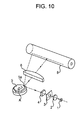
- Fig. 10 is a schematic diagram illustrating the main portion of a conventional optical scanning apparatus.
- a divergent light beam is emitted form a light source 1 and is collimated by a collimating lens 2. Then, the collimated light beam is incident on a cylindrical lens 4 having a predetermined refractive power only in a sub-scanning direction after the width of the light beam is restricted by a diaphragm 3.
- the collimated light beam incident on the cylindrical lens 4 exits the cylindrical lens 4 without a change in a main-scanning cross section (plane).
- the light beam converges in a sub-scanning cross section (plane), thereby forming a line image on a deflecting surface (reflective surface) 5a of the polygon mirror 5.
- the light beam is deflected and scanned by the deflecting surface 5a of the polygon mirror 5 and is guided toward a photosensitive drum surface 8, which functions as a surface to be scanned, through an f ⁇ lens 6.
- the polygon mirror 5 is rotated in the direction shown by the arrow A, so that the photosensitive drum surface 8 is optically scanned in the direction shown in the figure and image information is recorded thereon (refer to, for example, Japanese Patent Laid-Open No. 04-321370 and Japanese Patent Laid-Open No. 2002-40350 ).
- a semiconductor laser capable of direct modulation is used as a light source for an optical scanning apparatus.
- Power of light emitted from the semiconductor laser varies depending on heat emitted from the semiconductor laser itself and environmental variation (for example, ambient temperature variation).
- the power of light emitted is constantly detected and automatic power control is performed such that the power of the light beam emitted from a light-emitting portion of the light source is always maintained constant.
- a rear light beam that is emitted from a semiconductor laser in a direction opposite to the direction in which an image-drawing light beam is emitted i.e., a light beam emitted from a rear side of a semiconductor substrate
- a light beam emitted from a rear side of a semiconductor substrate is detected and used for the light-power control.
- the image-drawing light beam is a light beam used for forming dots in an image effective area on the photosensitive drum surface.
- a photosensor which functions as a light-power detector, can be installed in a package of the laser light source. Therefore, the overall size is relatively small and the light-power control for the light source can be easily performed.
- VCSEL vertical cavity surface emitting laser
- the vertical cavity surface emitting laser has been attracting attention as a light source for an optical scanning apparatus.
- the vertical cavity surface emitting laser is characterized in that the number of light-emitting points can be considerably increased, two-dimensional parallel integration is possible, and the layout of the light-emitting points is easy.
- the rear light beam is basically not emitted and it is difficult to use the light-power control method in which the rear light beam is used.
- Japanese Patent Laid-Open No. 04-321370 discusses a second method in which the light-power control is performed using a portion of a light beam emitted from a semiconductor laser that is blocked by an aperture diaphragm.
- light-power control (automatic power control) can be performed without being affected by heat emitted from the light source.
- the light used for the automatic power control is not the rear light beam used in the first method
- the blocked light beam which is different from the image-drawing light beam in practice, is used and it is still difficult to perform high-accuracy light-power control.
- Japanese Patent Laid-Open No. 2002-40350 discusses a third method in which light-power control (automatic power control) is performed by separating a portion of a light beam that travels from a light source to a deflecting unit with a half mirror and guiding the separated portion toward a light-receiving element (photosensor).
- an expensive optical element such as a half mirror, is required for separating a portion of the image-drawing light beam.
- the output of the edge emitting laser is generally several tens of milliwatts, whereas the output of the vertical cavity surface emitting laser is generally less than several milliwatts. Therefore, when the vertical cavity surface emitting laser is used, the loss in the power of the image-drawing light beam is a serious problem.
- the present invention is directed to an inexpensive, simple automatic power control method with which light-power control can be performed without causing loss in power of image-drawing light beam.
- the light-power control is performed using an image-drawing light beam that is actually used, so that a vertical cavity surface emitting laser, which is a low-output light source, can be used.
- the light-power control is performed using an image-drawing light beam that is actually used, so that high-accuracy light-power control can be performed. Accordingly, high-speed, high-definition optical scanning apparatus and image-forming apparatus can be obtained and the size and cost thereof can be reduced.
- an optical scanning apparatus as specified in claims 1 to 11.
- the storage time of the light beam on the light-power-detection optical unit is increased and variation in the power of light emitted by the light source due to heat generated by the light source and environmental variation is accurately detected.
- the power of light emitted from the light-emitting portions of the light source can be maintained constant.
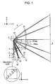
- Fig. 1 is a main-scanning sectional view of an optical scanning apparatus according to a first embodiment of the present invention.
- Fig. 2 is a main-scanning sectional view of an incident optical unit and a light-power detector included in the optical scanning apparatus according to the first embodiment of the present invention.
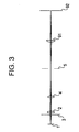
- Fig. 3 is a sub-scanning sectional view of the incident optical unit and the light-power detector included in the optical scanning apparatus according to the first embodiment of the present invention.
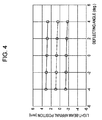
- Fig. 4 is a diagram illustrating the manner in which a light beam on the light-power detector moves in response to the rotation of a deflecting unit according to the first embodiment of the present invention.
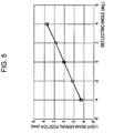
- Fig. 5 is a diagram illustrating the manner in which a light beam on a synchronization detector moves in response to the rotation of a deflecting unit according to the first embodiment of the present invention.
- Fig. 6 illustrates an image-forming apparatus according to a third embodiment of the present invention.
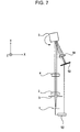
- Fig. 7 is a main-scanning sectional view of an incident optical unit and a light-power detector included in an optical scanning apparatus according to a second embodiment of the present invention.
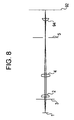
- Fig. 8 is a sub-scanning sectional view of the incident optical unit and the light-power detector included in the optical scanning apparatus according to the second embodiment of the present invention.
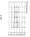
- Fig. 9 is a diagram illustrating the manner in which a light beam on the light-power detector moves in response to the rotation of a deflecting unit according to the second embodiment of the present invention.
- Fig. 10 is a perspective view of a conventional optical scanning apparatus.
- Fig. 11 is a main-scanning sectional view of the optical scanning apparatus according to the second embodiment of the present invention.
- Fig. 12 is a time chart of light-power detection according to the first embodiment of the present invention.
- the automatic power control is performed to stabilize the output of a light beam (laser beam), which is used for raster scanning a photosensitive drum surface to form an electrostatic latent image, with respect to temperature variation.
- the light beam (laser beam) is output from a light-emitting element of a light source and is detected (for example, once every horizontal scanning) by a light-power detector, and the thus obtained output signal is fed back to a laser driving circuit. Accordingly, the intensity (light-power) of the light beam (laser beam) is controlled such that the output of the light beam (laser beam) is maintained constant at a predetermined set value (refer to, for example, Japanese Patent Laid-Open No. 05-30314 ).
- Fig. 1 is a sectional view taken along a main-scanning direction (hereafter called a main-scanning sectional view) of an optical scanning apparatus according to a first embodiment of the present invention.
- Fig. 2 is a main-scanning sectional view of an incident optical system and a light-power-detecting optical system included in the optical scanning apparatus according to the first embodiment.
- Fig. 3 is a sectional view taken along a sub-scanning direction (hereafter called a sub-scanning sectional view) of the incident optical system and the light-power-detecting optical system included in the optical scanning apparatus according to the first embodiment.
- the main-scanning direction refers to a direction perpendicular to a rotating axis of a deflecting unit (direction in which a light beam is scanned) and the sub-scanning direction refers to a direction parallel to the rotating axis of the deflecting unit (direction in which an image carrier is moved).
- a semiconductor laser 1 which functions as a light source, is a vertical cavity surface emitting laser and includes four light-emitting points.
- Fig. 1 As shown in Fig. 1 , four light-emitting portions are arranged along a line, the line being disposed at predetermined angles relative to the main-scanning direction (Y direction) and the sub-scanning direction (X direction).
- Fig. 1 For simplicity, only one light beam (laser beam) is shown in Fig. 1 .
- Four divergent light beams emitted from the semiconductor laser 1 are converted into four collimated light beams by a common collimating lens 2 after the widths thereof in the main-scanning direction and the sub-scanning direction are restricted by a diaphragm 3.
- the four light beams are incident on a cylindrical lens 4 having a refractive power only in the sub-scanning direction and are focused on a deflecting surface of a rotating polygon mirror 5, which functions as a deflecting unit, in the sub-scanning direction.
- the collimated light beams are incident on the reflective surface of the polygon mirror 5 without a change.
- An imaging optical system 6 establishes a conjugate relationship between the deflecting surface of the polygon mirror 5 and a photosensitive drum surface in the sub-scanning cross section (plane). Accordingly, a surface-tilt correcting system is provided in the optical scanning apparatus according to the present embodiment.
- the polygon mirror 5 which functions as a deflecting unit, is rotated by a drive unit (not shown), such as a motor, at a constant speed in the direction shown by the arrow.
- a drive unit such as a motor
- the four light beams deflected and scanned by the polygon mirror 5 are incident on the imaging optical system 6 having an f ⁇ characteristic.
- the imaging optical system 6 includes two toric lenses 61 and 62 composed of plastic.
- the four light beams are guided toward a photosensitive drum surface 8, which functions as a surface to be scanned.
- the photosensitive drum surface 8 is optically scanned in the +Y direction by rotating the polygon mirror 5 in the direction shown by the arrow.
- scanning lines are formed on the photosensitive drum surface 8 and image recording is performed.
- portions of the light beams that travel toward an area outside an image effective area are guided toward a synchronization detection sensor 72 through a synchronization-detection optical element 71.
- the synchronization detection sensor 72 outputs a synchronization detection signal for determining timing for writing an image.
- a light-power detection sensor 92 which functions as a light-power detector, thought a light-power detection optical element 91.
- the light-power detection sensor 92 outputs a signal for controlling the power of light emitted from the light source (automatic power control).
- the light beams are deflected by the deflecting unit, and then the light-power control for the light source 1 is performed using the deflected light beams. Accordingly, the following characteristics are provided.
- the light source according to the present embodiment is a vertical cavity surface emitting laser (VCSEL) having four light-emitting points that are arranged adjacent to each other.
- VCSEL vertical cavity surface emitting laser
- the vertical cavity surface emitting laser In the vertical cavity surface emitting laser, light is emitted in a direction perpendicular to the semiconductor substrate. Therefore, compared to a conventional edge emitting laser, the number of light-emitting points can be considerably increased, two-dimensional parallel integration is possible, and the layout of the light-emitting points is easy.
- the power of light emitted from each light-emitting point is small compared to that of the edge emitting laser.
- the rear light beam is not emitted. Therefore, the light-power control is difficult.
- the following structure is provided in the light-power control method (automatic power control method) according to the present invention.
- the synchronization detection sensor 72 can be scanned with light at a high speed and the light beams can be focused on the synchronization detection sensor 72 or on the synchronization detection slit 73 disposed in front of the synchronization detection sensor 72 at least in the main-scanning direction.
- the synchronization-detection optical element 71 focuses the collimated light beams from the polygon mirror 5 on the synchronization detection sensor 72 or on the slit 73 disposed in front of the synchronization detection sensor 72 in the main-scanning direction.
- the power of the synchronization-detection optical element 71 is set such that all of the divergent light from the polygon mirror is incident on a light-receiving surface of the synchronization detection sensor 72.
- a storage time at the light-power detection sensor 92 must be a predetermined time or more, and the light beams can be stationary on the light-power detection sensor 92 during that time.
- the light-power detection optical element 91 is disposed so as to establish a conjugate relationship between the deflecting surface of the polygon mirror 5 and the light-receiving surface of the light-power detection sensor 92 in the main-scanning direction.
- Fig. 2 the solid line shows the actual light beam and the dashed lines show the conjugate (imaging) relationship.
- the collimated light beams from the polygon mirror 5, which functions as a deflecting unit are once caused to converge at a position between the light-power detection optical element 91 and the light-power detection sensor 92 by the light-power detection optical element 91, and are then incident on the light-power detection sensor 92 in the form of divergent light.
- the light beams are stationary on the light-receiving surface of the light-power detection sensor 92.
- the light beams form line images that extend in the main-scanning direction on the light-receiving surface of the light-power detection sensor 92, similar to the deflecting surface of the polygon mirror 5.
- the light-power detection sensor 92 detects the intensities (powers) of the light beams on the light-receiving surface thereof, and outputs intensity signals to the light-power controller 93 (automatic power control circuit).
- the light-power controller 93 (automatic power control circuit) outputs intensity correction signals to four light-emitting portions 1a, 1b, 1c, and 1d in the light source 1 so that the intensities (powers) of the light beams emitted from the four light-emitting portions 1a, 1b, 1c, and 1d are maintained as a predetermined set value.
- the cylindrical lens 4, the light-power detection optical element 91, and the synchronization-detection optical element 71 are composed of plastic and are formed integrally by injection molding.
- the semiconductor laser 1, the light-power detection sensor 92, and the synchronization detection sensor 72 are arranged on the same substrate.
- the light-power control for the light source can be performed using a small, inexpensive structure.
- the light-power detection optical element may also be formed integrally with other components, such as the collimating lens, the diaphragm, etc.
- Table 1 shows the optical design values of the structure along the optical path from the light source to the light-power detector via the deflecting unit.
- the light beams are completely stationary on the light-power detection sensor 92 in a paraxial area.
- the light-power detection optical element 91 is a spherical lens
- the light beams slightly move due to the spherical aberration of the light-power detection optical element 91 in the main-scanning cross section (plane).
- the incident surface of the light-power detection optical element 91 is formed as a rotationally symmetrical aspheric surface so that the spherical aberration can be corrected.
- X h 2 R 1 + 1 - 1 + k ⁇ h R 2
- the length of the light-power detection sensor 92 in the main-scanning direction must be larger than the beam diameter of the light beams on the light-power detection sensor 92 in the main-scanning direction.
- the correction of the spherical aberration of the light-power detection optical element 91 is also important from the standpoint of reduction in size of the light-power detection sensor 92.
- Fig. 4 illustrates the manner in which a light beam on the light-power detection sensor 92 moves in response to the rotation of the polygon mirror 5 according to the present embodiment.
- Fig. 5 shows the movement of a light beam on the synchronization detection sensor 72.
- the dot-dash line shows the principal ray of the light beam and the solid lines show the marginal rays of the light beam in the main-scanning direction.
- the two marginal rays in the main-scanning direction are an upper ray and a lower ray.
- the horizontal axis shows the deflecting angle of the light beam (positional reference of the light-power detection sensor 92) and the vertical axis shows the arrival position of the light beam (positional reference of the light-power detection sensor 92).
- the optical axis of the light-power detection optical system (the optical axis of the light-power detection optical element 91) is set as a reference (zero) of the light-beam arrival position in the main-scanning cross section (plane).
- a clockwise movement of the light beam (direction in which the light-receiving surface is scanned by the light beam) is defined as negative and a counterclockwise movement of the light beam (direction in which the light beam approaches the imaging optical system 6 in the main-scanning direction) is defined as positive.
- the principal ray and the outermost rays of the light beam coincide with one another on the light-receiving surface of the synchronization detection sensor 72 in the main-scanning cross section (plane). More specifically, in the main-scanning cross section (plane), the light beam is focused on the light-receiving surface of the synchronization detection sensor 72.
- the deflecting surface of the polygon mirror 5 and the light-receiving surface of the synchronization detection sensor 72 are not in an optically conjugate relationship.
- the deflecting angle of the polygon mirror 5 changes, the light beam arrival position on the light-receiving surface of the synchronization detection sensor 72 in the main-scanning direction largely changes while the light beam is being incident on the synchronization-detection optical element 71.
- the scanning angular velocity Vapc on the light-power detection sensor 92 in the light-power-detection optical system can satisfy the following expression: Vapc ⁇ f / 10 where f is the f ⁇ coefficient (mm/rad) of the optical scanning apparatus.
- Vapc is 3.2 (mm/rad) and f is 150 (mm/rad).
- the light beams incident on the imaging optical system 6 are collimated. Therefore, the f ⁇ coefficient f of the optical scanning apparatus is equal to the focal length of the imaging optical system 6.
- the f ⁇ coefficient is the moving distance of the light beams on the scanned surface per unit deflecting angle of the polygon mirror 5, and indicates the scanning angular velocity of the optical scanning apparatus.
- An imaging magnification ⁇ am between the deflecting surface of the deflecting unit and the light-receiving surface of the light-power detection sensor 92 provided by the light-power detection optical element 91 in the main-scanning direction can satisfy the following expression: 0.05 ⁇ ⁇ am ⁇ 1.5
- the light-power-detection optical unit establishes an optically conjugate relationship between the deflecting surface of the deflecting unit and the light-receiving surface of the light-power detection sensor 92.
- the light beams deflected and scanned by the deflecting surface are incident on the light-power detection optical element 91, the light beams incident on the light-receiving surface of the light-power detection sensor 92 are optically stationary on the light-receiving surface.
- the storage time of the light beams on the light-power detector can be increased and variation in the power of light emitted by the light source (variations in the intensities of the light beams) due to heat generated by the light source itself and environmental variation (for example, ambient temperature variation) can be accurately detected.
- the powers of the light beams emitted from the light-emitting portions of the light source can be maintained constant.
- the time in which the light beams can be kept stationary on the light-receiving surface of the light-power detection sensor 92 is limited to the time in which the light beams deflected by the deflecting unit are incident on the light-power detection optical element 91.
- the light-power control (light-beam-intensity adjustment) is performed by successively turning on the four light-emitting portions one at a time in each scanning cycle. Accordingly, the light-power control for all of the light-emitting portions is completed after four scanning cycles.
- the light-power control (light-beam-intensity adjustment) is performed by successively turning on the four light-emitting portions one at a time in each scanning cycle using a single deflecting surface of the polygon mirror.
- the light-power control for all of the light-emitting portions is completed after the polygon mirror is rotated by one turn.
- the light-power adjustment is successively performed for the light-emitting portions one at a time in each scanning cycle, so that the light-power adjustment for all of the light-emitting portions in the light source is completed after a plurality of scanning cycles.
- a single scanning cycle corresponds to a scanning process performed by a single surface of the polygon mirror.
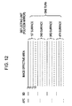
- Fig. 12 is a timing chart of scanning lines drawn for the automatic power control (APC) and synchronization detection and those drawn in the image effective area on the photosensitive drum surface 8.
- API automatic power control
- the automatic power control (APC) and the synchronization detection for controlling the light-emitting portions of the light source 1 are performed in that order before the four scanning lines 1a, 1b, 1c, and 1d are drawn in the image effective area using a first surface of the deflecting unit 5 (four-surface polygon mirror).
- write start positions on the photosensitive drum surface 8 in the main-scanning direction are determined on the basis of the synchronization detection signal obtained by detecting the light beam corresponding to the scanning line 1a.
- the write start position on the photosensitive drum surface 8 in the main-scanning direction (write start time) for the light beam corresponding to the scanning line 1a is, of course, also determined by the synchronization detection signal obtained by detecting the light beam corresponding to the scanning line 1a.
- the light-power control can be performed by the above-described sequence for the case in which the number of light-emitting portions is increased.
- the effects of the present invention can also be obtained when the four light-emitting portions are divided into two pairs and the light-power control is successively performed one pair at a time.
- the present invention is not limited to the above-described sequence.
- Fig. 11 is a main-scanning sectional view of an optical scanning apparatus according to a second embodiment of the present invention.
- Fig. 7 is a main-scanning sectional view of an incident optical system including components 2, 3, and 4 and a light-power detection optical system included in the optical scanning apparatus according to the second embodiment of the present invention.
- Fig. 8 is a sub-scanning sectional view of the incident optical system including components 2, 3, and 4 and the light-power detection optical system included in the optical scanning apparatus.
- the present embodiment differs from the first embodiment in that an edge emitting monolithic multilaser is used as a light source 1 and the imaging magnification of the light-power detection optical system is reduced.
- Other structures of the present embodiment are similar to those of the first embodiment.
- the semiconductor laser 1 which functions as a light source, is an edge emitting monolithic multilaser including two light-emitting portions.
- These two light-emitting points are arranged along respective lines that are disposed at predetermined angles relative to the main-scanning direction and the sub-scanning direction (see Fig. 11 ).
- Two divergent light beams output from two light-emitting portions of the semiconductor laser 1 are converted into two collimated light beams by a common collimating lens 2 after the widths thereof in the main-scanning direction and the sub-scanning direction are restricted by a diaphragm 3.
- the two light beams are incident on a cylindrical lens 4 having a refractive power only in the sub-scanning direction, and are focused on a reflective surface of a rotating polygon mirror 5 in the sub-scanning cross section.
- the two collimated light beams are incident on the reflective surface of the polygon mirror 5 (four-surface polygon mirror) without a change.
- the polygon mirror 5 which functions as a deflecting unit, is rotated by a drive unit (not shown), such as a motor, at a constant speed in the direction shown by the arrow.
- a drive unit such as a motor
- the two light beams deflected and scanned by the polygon mirror 5 are incident on an imaging optical system 6 having an f ⁇ characteristic, and are then guided toward a photosensitive drum surface 8, which is a surface to be scanned.
- image recording is performed.
- the imaging optical system 6 establishes an optically conjugate relationship between the deflecting surface of the polygon mirror 5 and a photosensitive drum surface in the sub-scanning cross section. Accordingly, a surface-tilt correcting system is provided in the optical scanning apparatus according to the present embodiment.
- the imaging optical system 6 includes two toric lens 61 and 62 composed of plastic.
- the two light beams are guided toward the photosensitive drum surface 8.
- the photosensitive drum surface 8 is optically scanned in +Y direction by rotating the polygon mirror 5 in the direction shown by the arrow.
- portions of the light beams that travel toward an area outside an image effective area are guided toward a synchronization detection sensor 72 through a synchronization-detection optical element 71.
- the synchronization detection sensor 72 outputs a synchronization detection signal for determining timing for writing an image (write start position in the main-scanning direction).
- portions of the light beams that travel toward an area outside an image effective area are guided toward a light-power detection sensor 92, which functions as a light-power detector, through a light-power detection optical element 94.
- the light-power detection sensor 92 outputs a signal for controlling the power (intensity) of light emitted from the light source.
- light beams are deflected by the deflecting unit 5, and then the light-power control for the light source is performed using the deflected light beams.
- the light-power detection sensor 92 detects the intensities (powers) of the light beams on the light-receiving surface thereof, and outputs intensity signals to a light-power controller 93 (automatic power control circuit).
- the light-power controller 93 (automatic power control circuit) outputs intensity correction signals for the two light-emitting portions 1a and 1b in the light source 1, which is an edge emitting laser, so that the intensities (powers) of the light beams emitted from the two light-emitting portions 1a and 1b are maintained as a predetermined set value.
- the light source 1 is an edge emitting laser having two light-emitting points that are arranged adjacent to each other.
- edge emitting laser light is emitted in a direction perpendicular to an end face of the substrate and the output power can be easily increased compared to a surface emitting laser.
- a rear light beam is emitted from the other end face of the substrate, and the light-power control can also be performed by directly monitoring the rear light beam.
- the light-power control (automatic power control) is performed using a light beam that is not actually used for drawing an image.
- the light-receiving surface is easily affected by heat generated by the edge emitting laser itself. Therefore, it is difficult to perform high-accuracy light-power control.
- the light-power detection optical element 94 is disposed so as to establish an optically conjugate relationship between the deflecting surface of the deflecting unit 5 and the light-receiving surface of the light-power detection sensor 92 in the main-scanning direction.
- the light beams deflected by the deflecting surface are incident on the light-power detection optical element 94, the light beams incident on the light-receiving surface of the light-power detection sensor 92 are optically stationary on the light-receiving surface.
- the storage time of the light beams on the light-power detector 92 can be increased and variation in the power of light emitted by the light source 1 due to heat generated by the light source 1 itself and environmental variation (for example, ambient temperature variation) can be accurately detected.
- the powers of the light beams emitted from the light-emitting portions of the light source 1 can be maintained constant.
- the collimated light beams deflected and scanned by the deflecting surface are once focused at a position between the light-power detection optical element 94 and the light-power detection sensor 92, and are then incident on the light-receiving surface of the light-power detection sensor 92.
- the dashed lines show that the deflecting surface of the polygon mirror 5 and the light-receiving surface of the light-power detection sensor 92 are in the optically conjugate relationship in the main-scanning cross section.
- the collimated light beams from the polygon mirror 5, which functions as a deflecting unit are caused to converge at a position between the light-power detection optical element 94 and the light-power detection sensor 92 by the light-power detection optical element 94, and are then incident on the light-receiving surface of the light-power detection sensor 92 in the form of the divergent light.
- the light beams form line images that extend in the main-scanning direction on the light-receiving surface, similar to the deflecting surface.
- the cylindrical lens 4 and the light-power detection optical element 94 are formed separately from each other.
- the semiconductor laser 1 and the light-power detection sensor 92 are formed on different substrates.
- the sensor size can be further reduced by reducing the moving velocity of the light beams and the diameters of the light beams on the sensor.
- the light-power control (light-beam intensity adjustment) is performed by successively turning on the two light-emitting portions one at a time in each scanning cycle using a single deflecting surface of the polygon mirror. Accordingly, the light-power control for the two light-emitting portions is completed after the polygon mirror is rotated by a half turn.
- Table 2 shows the optical design values of the structure along the optical path from the light source 1 to the light-power detection sensor 92 via the deflecting unit 5.
- the light beams are completely stationary in the main-scanning direction on the light-receiving surface of the light-power detection sensor 92 in a paraxial area.
- the light beams slightly move on the light-receiving surface in practice due to the spherical aberration of the light-power detection optical element 94 in the main-scanning cross section.
- the incident surface of the light-power detection optical element 94 is formed as a rotationally symmetrical aspheric surface so that the spherical aberration can be corrected.
- the incident surface of the light-power detection optical element 94 has a non-arc shape in the main-scanning cross section.
- the length of the light-receiving surface of the light-power detection sensor 92 in the main-scanning direction must be larger than the beam diameter of the light beams on the light-power detection sensor 92 in the main-scanning direction.
- Fig. 9 illustrates the manner in which a light beam on the light-power detection sensor 92 moves in response to the rotation of the deflecting unit 5.
- the dot-dash line shows the principal ray of the light beam and the solid lines show the marginal rays of the light beam in the main-scanning direction.
- the two marginal rays in the main-scanning direction are an upper ray and a lower ray.
- the horizontal axis shows the deflecting angle of the light beam (positional reference of the light-power detection sensor 92) and the vertical axis shows the arrival position of the light beam (positional reference of the light-power detection sensor 92).
- the optical axis of the light-power detection optical system (the optical axis of the light-power detection optical element 94) is set as a reference (zero) of the light-bam arrival position in the main-scanning cross section.
- a clockwise movement of the light beam (direction in which the light-receiving surface is scanned by the light beam) is defined as negative and a counterclockwise movement of the light beam (direction in which the light beam approaches the imaging optical system 6 in the main-scanning direction) is defined as positive.
- the scanning angular velocity Vapc on the light-power detection sensor in the light-power detection optical system can satisfy the following expression: Vapc ⁇ f / 10 where f is the f ⁇ coefficient (mm/rad) of the optical scanning apparatus.
- f is the f ⁇ coefficient (mm/rad) of the optical scanning apparatus.
- Vapc is 1.3 (mm/rad) and f is 150 (mm/rad).
- An imaging magnification ⁇ am between the deflecting surface of the deflecting unit 5 and the light-receiving surface of the light-power detection sensor 92 provided by the light-power detection optical element 91 in the main-scanning direction can satisfy the following expression: 0.05 ⁇ ⁇ am ⁇ 1.5
- the light-power detection optical element in the structure for performing the automatic power control of the light source 1 in the optical scanning apparatus, establishes an optically conjugate relationship between the deflecting surface of the deflecting unit and the light-receiving surface of the light-power detection sensor 92 in the main scanning direction.
- the light beams on the light-receiving surface of the light-power detection sensor 92 are optically stationary in the main-scanning direction.
- a low-output light source such as a vertical cavity surface emitting laser, can be used.
- a vertical cavity surface emitting laser including a plurality of light-emitting portions (4 beam) and an edge emitting monolithic multilaser including a plurality of light-emitting portions (2 beam) are used.
- the present invention is not limited to multibeam lasers.
- the effects of the present invention can also be obtained when a single-beam laser having a single light-emitting portion is used as the light source.
- the number of light-emitting portions of the multibeam laser is not limited as long as two or more light-emitting portions are provided. Since there is a growing demand for high-speed processes, the structure of the present invention can be effectively used in multibeam lasers that emit four or more light beams.
- the imaging optical system 6 includes two toric lenses 61 and 62.
- the present invention is not limited to this.
- the imaging optical system 6 may also be composed of a single toric lens.
- the imaging optical system 6 may also be composed of three or more lenses.
- the imaging optical system 6 may include a curved mirror or a diffractive optical element.
- Fig. 6 is a schematic diagram illustrating the main portion of a color image-forming apparatus according to a third embodiment of the present invention.
- a color image-forming apparatus 160 includes optical scanning apparatus 110, which each have the structure according to the above-described first embodiment, photosensitive drums 121, 122, 123 and 124 which each can function as an image carrier, developing devices 131, 132, 133 and 134, and a conveying belt 151.
- the color image-forming apparatus 160 receives red (R), green (G), and blue (B) signals from an external device 152, such as a personal computer.
- These signals are respectively converted into image data elements (dot data elements) 141, 142, 143, and 144 for cyan (C), magenta (M), yellow (Y), and black (K), respectively, by a printer controller 153 included in the color image-forming apparatus 160.
- the image data elements are input to the corresponding optical scanning apparatuses 110.
- Each of the four optical scanning apparatuses 110 emits four light beams that are modulated in accordance with the corresponding image data element, and photosensitive surfaces of the photosensitive drums 121, 122, 123 and 124 are scanned in the main scanning direction by the 4 ⁇ 4 light beams.
- the 4 ⁇ 4 light beams emitted from the optical scanning apparatuses 110 in accordance with the respective image data elements are used to form latent images of the respective colors on the corresponding photosensitive drums 121, 122, 123, and 124. Then, the images are superimposed on a recording medium to obtain a single, full color image.
- Reference numerals 131, 132, 133, and 134 denote developing devices. As described above, the light beams are modulated on the basis of the image data elements, and the surfaces of the photosensitive drums 121, 122, 123 and 124 are irradiated with the light beams so that electrostatic latent images are formed on the surfaces thereof.
- the electrostatic latent images are developed as toner images by the developing devices 131, 132, 133, and 134 disposed such that the developing devices 131, 132, 133, and 134 are in contact with the photosensitive drums 121, 122, 123 and 124, respectively, at positions on the downstream of the positions at which the photosensitive drums 131, 132, 133, and 134 are irradiated with the light beams in the rotating direction of the photosensitive drums 131, 132, 133, and 134.
- the toner images developed by the developing devices 131, 132, 133, and 134 are transferred onto a paper sheet that can function as a transferring material by transferring rollers (not shown) disposed below the photosensitive drums 121, 122, 123 and 124 so as to face the photosensitive drums 121, 122, 123 and 124.
- transferring rollers not shown
- the paper sheet is fed from a paper cassette disposed in front of the photosensitive drums 121, 122, 123 and 124 in this example, it can also be fed manually.
- a paper feed roller that is disposed at an end of the paper cassette conveys the paper sheet contained in the paper cassette to a transporting path.
- the paper sheet on which the unfixed toner image is transferred as described above is further transported to a fixing device (not shown) disposed behind the photosensitive drums 121, 122, 123 and 124.
- the fixing device includes a fixing roller (not shown), which can have a fixing heater (not shown) therein, and a pressure roller (not shown) disposed so as to be in pressure contact with the fixing roller.
- the paper sheet conveyed from the transferring section is pressed and heated in a nip portion between the fixing roller and the pressure roller so that the unfixed toner image on the paper is fixed.
- Paper output rollers (not shown) are disposed behind the fixing roller and the paper sheet on which the image is fixed is output from the image-forming apparatus.
- the external device 152 can include, for example, a color image reading apparatus, which can have a CCD sensor.
- a system including the color image reading apparatus and the color image-forming apparatus 160 can function as a color digital copying machine.
- the optical scanning apparatus is not limited to color digital copy machines, and may also be applied to color laser beam printers, monochrome digital copy machines, monochrome laser beam printers, etc..
- optical scanning apparatus can also be applied to image-forming apparatus, such as laser beam printers and digital copy machines, that perform electrophotography processes.
Landscapes
- Physics & Mathematics (AREA)
- General Physics & Mathematics (AREA)
- Optics & Photonics (AREA)
- Engineering & Computer Science (AREA)
- Multimedia (AREA)
- Signal Processing (AREA)
- Facsimile Scanning Arrangements (AREA)
- Mechanical Optical Scanning Systems (AREA)
- Laser Beam Printer (AREA)
Applications Claiming Priority (1)
| Application Number | Priority Date | Filing Date | Title |
|---|---|---|---|
| JP2005297617A JP4642627B2 (ja) | 2005-10-12 | 2005-10-12 | 走査光学装置及びそれを用いた画像形成装置 |
Publications (2)
| Publication Number | Publication Date |
|---|---|
| EP1775622A1 EP1775622A1 (en) | 2007-04-18 |
| EP1775622B1 true EP1775622B1 (en) | 2009-08-26 |
Family
ID=37621956
Family Applications (1)
| Application Number | Title | Priority Date | Filing Date |
|---|---|---|---|
| EP06122049A Not-in-force EP1775622B1 (en) | 2005-10-12 | 2006-10-10 | Optical scanning apparatus and image-forming apparatus using the same |
Country Status (8)
Families Citing this family (7)
| Publication number | Priority date | Publication date | Assignee | Title |
|---|---|---|---|---|
| JP5147331B2 (ja) | 2006-08-23 | 2013-02-20 | キヤノン株式会社 | レーザ光制御装置及び画像形成装置 |
| JP2010122473A (ja) * | 2008-11-20 | 2010-06-03 | Ricoh Co Ltd | 光源装置、光走査装置及び画像形成装置 |
| JP5489073B2 (ja) * | 2010-06-02 | 2014-05-14 | 株式会社リコー | 画像形成装置 |
| JP5573493B2 (ja) | 2010-08-25 | 2014-08-20 | 株式会社リコー | 光走査装置及び画像形成装置 |
| US8976423B2 (en) * | 2013-03-15 | 2015-03-10 | Lexmark International, Inc. | Optical scanning system and imaging apparatus for using same |
| WO2021002286A1 (ja) * | 2019-07-04 | 2021-01-07 | コニカミノルタ株式会社 | 分光測定器 |
| JP2024087228A (ja) * | 2022-12-19 | 2024-07-01 | キヤノン株式会社 | 光学走査装置及び画像形成装置 |
Family Cites Families (21)
| Publication number | Priority date | Publication date | Assignee | Title |
|---|---|---|---|---|
| JPS6138922A (ja) * | 1984-07-31 | 1986-02-25 | Fuji Photo Film Co Ltd | 光ビ−ム走査装置 |
| JPS6350811A (ja) * | 1986-08-21 | 1988-03-03 | Minolta Camera Co Ltd | レ−ザ−ビ−ムプリンタ |
| US5497184A (en) * | 1990-04-27 | 1996-03-05 | Asahi Kogaku Kogyo Kabushiki Kaisha | Laser scanning system |
| JPH04321370A (ja) | 1991-04-19 | 1992-11-11 | Canon Inc | 走査光学装置 |
| JPH0530314A (ja) | 1991-07-25 | 1993-02-05 | Canon Inc | 画像形成装置 |
| JPH05215981A (ja) | 1992-02-05 | 1993-08-27 | Fuji Photo Optical Co Ltd | 光走査装置 |
| US5671077A (en) * | 1992-05-18 | 1997-09-23 | Ricoh Company, Ltd. | Multi-beam light source device and optical scanning apparatus using the multi-beam source device |
| JP2908657B2 (ja) | 1992-05-18 | 1999-06-21 | 株式会社リコー | 半導体レーザアレイ記録装置 |
| US5357106A (en) * | 1993-10-01 | 1994-10-18 | Xerox Corporation | Sensor for detecting beam position and start of scan position |
| JPH07104204A (ja) * | 1993-10-07 | 1995-04-21 | Ricoh Co Ltd | 光走査装置 |
| US5959655A (en) * | 1995-05-30 | 1999-09-28 | Hitachi, Ltd. | Light beam scanning apparatus which controls power and spot shape of light beam |
| JP4364327B2 (ja) * | 1998-11-24 | 2009-11-18 | フジノン株式会社 | 光走査装置の同期光検出装置 |
| JP3667205B2 (ja) * | 1999-07-30 | 2005-07-06 | キヤノン株式会社 | 画像形成装置 |
| JP2001201704A (ja) * | 2000-01-21 | 2001-07-27 | Ricoh Co Ltd | 光走査装置 |
| JP2002040350A (ja) | 2000-07-28 | 2002-02-06 | Fuji Xerox Co Ltd | 光走査装置 |
| JP4590111B2 (ja) * | 2001-01-30 | 2010-12-01 | キヤノン株式会社 | 光走査装置及びそれを有する画像形成装置 |
| JP2004021171A (ja) | 2002-06-20 | 2004-01-22 | Canon Inc | 光走査装置及びそれを用いた画像形成装置 |
| JP4363015B2 (ja) * | 2002-09-19 | 2009-11-11 | 富士ゼロックス株式会社 | 光走査装置 |
| JP2005202042A (ja) * | 2004-01-14 | 2005-07-28 | Canon Inc | 走査光学装置 |
| US7119825B2 (en) * | 2004-01-21 | 2006-10-10 | Xerox Corporation | Parallel beam to beam power correction |
| JP2007033832A (ja) * | 2005-07-26 | 2007-02-08 | Fuji Xerox Co Ltd | 光走査装置 |
-
2005
- 2005-10-12 JP JP2005297617A patent/JP4642627B2/ja not_active Expired - Fee Related
-
2006
- 2006-09-28 US US11/536,172 patent/US7466333B2/en not_active Expired - Fee Related
- 2006-10-10 EP EP06122049A patent/EP1775622B1/en not_active Not-in-force
- 2006-10-10 ES ES06122049T patent/ES2328844T3/es active Active
- 2006-10-10 AT AT06122049T patent/ATE441131T1/de not_active IP Right Cessation
- 2006-10-10 DE DE602006008717T patent/DE602006008717D1/de active Active
- 2006-10-12 CN CNB2006101321664A patent/CN100417971C/zh not_active Expired - Fee Related
- 2006-10-12 KR KR1020060099105A patent/KR100856154B1/ko not_active Expired - Fee Related
-
2008
- 2008-11-25 US US12/323,335 patent/US8063927B2/en not_active Expired - Fee Related
Also Published As
| Publication number | Publication date |
|---|---|
| KR100856154B1 (ko) | 2008-09-03 |
| US8063927B2 (en) | 2011-11-22 |
| ATE441131T1 (de) | 2009-09-15 |
| CN100417971C (zh) | 2008-09-10 |
| US7466333B2 (en) | 2008-12-16 |
| JP4642627B2 (ja) | 2011-03-02 |
| US20070081071A1 (en) | 2007-04-12 |
| CN1949022A (zh) | 2007-04-18 |
| DE602006008717D1 (de) | 2009-10-08 |
| EP1775622A1 (en) | 2007-04-18 |
| ES2328844T3 (es) | 2009-11-18 |
| US20090079810A1 (en) | 2009-03-26 |
| JP2007108298A (ja) | 2007-04-26 |
| KR20070040728A (ko) | 2007-04-17 |
Similar Documents
| Publication | Publication Date | Title |
|---|---|---|
| EP1775622B1 (en) | Optical scanning apparatus and image-forming apparatus using the same | |
| JP2009145569A (ja) | 走査光学装置及びそれを用いた画像形成装置 | |
| US7050209B2 (en) | Scanning optical apparatus and image forming apparatus using the same | |
| JP4474143B2 (ja) | 光走査装置の被走査面における像面位置の調整方法 | |
| JP3397765B2 (ja) | マルチビーム光走査光学系及びそれを用いた画像形成装置 | |
| JP4641478B2 (ja) | 光走査装置及びそれを用いた画像形成装置 | |
| JP4590166B2 (ja) | 光走査装置及びそれを用いた画像形成装置 | |
| KR100856163B1 (ko) | 광주사장치 및 화상형성장치 | |
| JP5173879B2 (ja) | 光走査装置及びそれを用いた画像形成装置 | |
| JP4593886B2 (ja) | 光走査装置及びそれを用いた画像形成装置 | |
| JP2002267968A (ja) | マルチビーム走査光学装置及びそれを用いた画像形成装置 | |
| JP2002131664A (ja) | 光走査装置及びそれを用いた画像形成装置 | |
| JP2006330581A (ja) | マルチビーム光走査装置及びそれを用いた画像形成装置 | |
| JP5127122B2 (ja) | 走査光学装置の走査線ピッチ間隔調整方法 | |
| JP4701010B2 (ja) | マルチビーム光走査装置及びそれを用いた画像形成装置 | |
| US20050046916A1 (en) | Optical scanning device and image forming apparatus using the same | |
| US20050057642A1 (en) | Scanning optical apparatus and image forming apparatus using the same | |
| JP4401950B2 (ja) | 光走査装置及びそれを用いた画像形成装置 | |
| JP4612839B2 (ja) | カラー画像形成装置の調整方法 | |
| JP2004317790A (ja) | 光走査装置 | |
| JP4401951B2 (ja) | 光走査装置及びそれを用いた画像形成装置 | |
| JP2004102006A (ja) | ポリゴンモーターユニット及びそれを用いた走査光学装置、画像形成装置 | |
| JP2004198894A (ja) | 走査光学装置及びそれを用いた画像形成装置 | |
| JP2009204940A (ja) | 光走査装置及びそれを用いた画像形成装置 | |
| JP2009271355A (ja) | 光走査装置及びそれを用いた画像形成装置 |
Legal Events
| Date | Code | Title | Description |
|---|---|---|---|
| PUAI | Public reference made under article 153(3) epc to a published international application that has entered the european phase |
Free format text: ORIGINAL CODE: 0009012 |
|
| AK | Designated contracting states |
Kind code of ref document: A1 Designated state(s): AT BE BG CH CY CZ DE DK EE ES FI FR GB GR HU IE IS IT LI LT LU LV MC NL PL PT RO SE SI SK TR |
|
| AX | Request for extension of the european patent |
Extension state: AL BA HR MK YU |
|
| 17P | Request for examination filed |
Effective date: 20071018 |
|
| AKX | Designation fees paid |
Designated state(s): AT BE BG CH CY CZ DE DK EE ES FI FR GB GR HU IE IS IT LI LT LU LV MC NL PL PT RO SE SI SK TR |
|
| GRAP | Despatch of communication of intention to grant a patent |
Free format text: ORIGINAL CODE: EPIDOSNIGR1 |
|
| GRAS | Grant fee paid |
Free format text: ORIGINAL CODE: EPIDOSNIGR3 |
|
| GRAA | (expected) grant |
Free format text: ORIGINAL CODE: 0009210 |
|
| AK | Designated contracting states |
Kind code of ref document: B1 Designated state(s): AT BE BG CH CY CZ DE DK EE ES FI FR GB GR HU IE IS IT LI LT LU LV MC NL PL PT RO SE SI SK TR |
|
| REG | Reference to a national code |
Ref country code: GB Ref legal event code: FG4D |
|
| REG | Reference to a national code |
Ref country code: CH Ref legal event code: EP |
|
| REG | Reference to a national code |
Ref country code: IE Ref legal event code: FG4D |
|
| REF | Corresponds to: |
Ref document number: 602006008717 Country of ref document: DE Date of ref document: 20091008 Kind code of ref document: P |
|
| REG | Reference to a national code |
Ref country code: ES Ref legal event code: FG2A Ref document number: 2328844 Country of ref document: ES Kind code of ref document: T3 |
|
| LTIE | Lt: invalidation of european patent or patent extension |
Effective date: 20090826 |
|
| PG25 | Lapsed in a contracting state [announced via postgrant information from national office to epo] |
Ref country code: IS Free format text: LAPSE BECAUSE OF FAILURE TO SUBMIT A TRANSLATION OF THE DESCRIPTION OR TO PAY THE FEE WITHIN THE PRESCRIBED TIME-LIMIT Effective date: 20091226 Ref country code: SE Free format text: LAPSE BECAUSE OF FAILURE TO SUBMIT A TRANSLATION OF THE DESCRIPTION OR TO PAY THE FEE WITHIN THE PRESCRIBED TIME-LIMIT Effective date: 20090826 Ref country code: LT Free format text: LAPSE BECAUSE OF FAILURE TO SUBMIT A TRANSLATION OF THE DESCRIPTION OR TO PAY THE FEE WITHIN THE PRESCRIBED TIME-LIMIT Effective date: 20090826 Ref country code: AT Free format text: LAPSE BECAUSE OF FAILURE TO SUBMIT A TRANSLATION OF THE DESCRIPTION OR TO PAY THE FEE WITHIN THE PRESCRIBED TIME-LIMIT Effective date: 20090826 Ref country code: FI Free format text: LAPSE BECAUSE OF FAILURE TO SUBMIT A TRANSLATION OF THE DESCRIPTION OR TO PAY THE FEE WITHIN THE PRESCRIBED TIME-LIMIT Effective date: 20090826 |
|
| PG25 | Lapsed in a contracting state [announced via postgrant information from national office to epo] |
Ref country code: PL Free format text: LAPSE BECAUSE OF FAILURE TO SUBMIT A TRANSLATION OF THE DESCRIPTION OR TO PAY THE FEE WITHIN THE PRESCRIBED TIME-LIMIT Effective date: 20090826 Ref country code: LV Free format text: LAPSE BECAUSE OF FAILURE TO SUBMIT A TRANSLATION OF THE DESCRIPTION OR TO PAY THE FEE WITHIN THE PRESCRIBED TIME-LIMIT Effective date: 20090826 Ref country code: SI Free format text: LAPSE BECAUSE OF FAILURE TO SUBMIT A TRANSLATION OF THE DESCRIPTION OR TO PAY THE FEE WITHIN THE PRESCRIBED TIME-LIMIT Effective date: 20090826 |
|
| PG25 | Lapsed in a contracting state [announced via postgrant information from national office to epo] |
Ref country code: BG Free format text: LAPSE BECAUSE OF FAILURE TO SUBMIT A TRANSLATION OF THE DESCRIPTION OR TO PAY THE FEE WITHIN THE PRESCRIBED TIME-LIMIT Effective date: 20091126 Ref country code: CY Free format text: LAPSE BECAUSE OF FAILURE TO SUBMIT A TRANSLATION OF THE DESCRIPTION OR TO PAY THE FEE WITHIN THE PRESCRIBED TIME-LIMIT Effective date: 20090826 Ref country code: PT Free format text: LAPSE BECAUSE OF FAILURE TO SUBMIT A TRANSLATION OF THE DESCRIPTION OR TO PAY THE FEE WITHIN THE PRESCRIBED TIME-LIMIT Effective date: 20091228 |
|
| PG25 | Lapsed in a contracting state [announced via postgrant information from national office to epo] |
Ref country code: RO Free format text: LAPSE BECAUSE OF FAILURE TO SUBMIT A TRANSLATION OF THE DESCRIPTION OR TO PAY THE FEE WITHIN THE PRESCRIBED TIME-LIMIT Effective date: 20090826 Ref country code: CZ Free format text: LAPSE BECAUSE OF FAILURE TO SUBMIT A TRANSLATION OF THE DESCRIPTION OR TO PAY THE FEE WITHIN THE PRESCRIBED TIME-LIMIT Effective date: 20090826 Ref country code: EE Free format text: LAPSE BECAUSE OF FAILURE TO SUBMIT A TRANSLATION OF THE DESCRIPTION OR TO PAY THE FEE WITHIN THE PRESCRIBED TIME-LIMIT Effective date: 20090826 Ref country code: DK Free format text: LAPSE BECAUSE OF FAILURE TO SUBMIT A TRANSLATION OF THE DESCRIPTION OR TO PAY THE FEE WITHIN THE PRESCRIBED TIME-LIMIT Effective date: 20090826 |
|
| PG25 | Lapsed in a contracting state [announced via postgrant information from national office to epo] |
Ref country code: SK Free format text: LAPSE BECAUSE OF FAILURE TO SUBMIT A TRANSLATION OF THE DESCRIPTION OR TO PAY THE FEE WITHIN THE PRESCRIBED TIME-LIMIT Effective date: 20090826 Ref country code: MC Free format text: LAPSE BECAUSE OF NON-PAYMENT OF DUE FEES Effective date: 20091031 |
|
| PG25 | Lapsed in a contracting state [announced via postgrant information from national office to epo] |
Ref country code: BE Free format text: LAPSE BECAUSE OF FAILURE TO SUBMIT A TRANSLATION OF THE DESCRIPTION OR TO PAY THE FEE WITHIN THE PRESCRIBED TIME-LIMIT Effective date: 20090826 |
|
| PLBE | No opposition filed within time limit |
Free format text: ORIGINAL CODE: 0009261 |
|
| STAA | Information on the status of an ep patent application or granted ep patent |
Free format text: STATUS: NO OPPOSITION FILED WITHIN TIME LIMIT |
|
| 26N | No opposition filed |
Effective date: 20100527 |
|
| PG25 | Lapsed in a contracting state [announced via postgrant information from national office to epo] |
Ref country code: IE Free format text: LAPSE BECAUSE OF NON-PAYMENT OF DUE FEES Effective date: 20091010 Ref country code: GR Free format text: LAPSE BECAUSE OF FAILURE TO SUBMIT A TRANSLATION OF THE DESCRIPTION OR TO PAY THE FEE WITHIN THE PRESCRIBED TIME-LIMIT Effective date: 20091127 |
|
| PG25 | Lapsed in a contracting state [announced via postgrant information from national office to epo] |
Ref country code: LU Free format text: LAPSE BECAUSE OF NON-PAYMENT OF DUE FEES Effective date: 20091010 |
|
| REG | Reference to a national code |
Ref country code: CH Ref legal event code: PL |
|
| PG25 | Lapsed in a contracting state [announced via postgrant information from national office to epo] |
Ref country code: HU Free format text: LAPSE BECAUSE OF FAILURE TO SUBMIT A TRANSLATION OF THE DESCRIPTION OR TO PAY THE FEE WITHIN THE PRESCRIBED TIME-LIMIT Effective date: 20100227 |
|
| PG25 | Lapsed in a contracting state [announced via postgrant information from national office to epo] |
Ref country code: LI Free format text: LAPSE BECAUSE OF NON-PAYMENT OF DUE FEES Effective date: 20101031 Ref country code: CH Free format text: LAPSE BECAUSE OF NON-PAYMENT OF DUE FEES Effective date: 20101031 |
|
| PG25 | Lapsed in a contracting state [announced via postgrant information from national office to epo] |
Ref country code: TR Free format text: LAPSE BECAUSE OF FAILURE TO SUBMIT A TRANSLATION OF THE DESCRIPTION OR TO PAY THE FEE WITHIN THE PRESCRIBED TIME-LIMIT Effective date: 20090826 |
|
| REG | Reference to a national code |
Ref country code: FR Ref legal event code: PLFP Year of fee payment: 10 |
|
| PGFP | Annual fee paid to national office [announced via postgrant information from national office to epo] |
Ref country code: IT Payment date: 20151005 Year of fee payment: 10 |
|
| PGFP | Annual fee paid to national office [announced via postgrant information from national office to epo] |
Ref country code: NL Payment date: 20150908 Year of fee payment: 10 Ref country code: ES Payment date: 20151014 Year of fee payment: 10 |
|
| REG | Reference to a national code |
Ref country code: FR Ref legal event code: PLFP Year of fee payment: 11 |
|
| REG | Reference to a national code |
Ref country code: NL Ref legal event code: MM Effective date: 20161101 |
|
| PG25 | Lapsed in a contracting state [announced via postgrant information from national office to epo] |
Ref country code: NL Free format text: LAPSE BECAUSE OF NON-PAYMENT OF DUE FEES Effective date: 20161101 |
|
| PG25 | Lapsed in a contracting state [announced via postgrant information from national office to epo] |
Ref country code: IT Free format text: LAPSE BECAUSE OF NON-PAYMENT OF DUE FEES Effective date: 20161010 |
|
| REG | Reference to a national code |
Ref country code: FR Ref legal event code: PLFP Year of fee payment: 12 |
|
| PG25 | Lapsed in a contracting state [announced via postgrant information from national office to epo] |
Ref country code: ES Free format text: LAPSE BECAUSE OF NON-PAYMENT OF DUE FEES Effective date: 20161011 |
|
| REG | Reference to a national code |
Ref country code: FR Ref legal event code: PLFP Year of fee payment: 13 |
|
| REG | Reference to a national code |
Ref country code: ES Ref legal event code: FD2A Effective date: 20181128 |
|
| PGFP | Annual fee paid to national office [announced via postgrant information from national office to epo] |
Ref country code: GB Payment date: 20181031 Year of fee payment: 13 Ref country code: FR Payment date: 20181025 Year of fee payment: 13 |
|
| PGFP | Annual fee paid to national office [announced via postgrant information from national office to epo] |
Ref country code: DE Payment date: 20181228 Year of fee payment: 13 |
|
| REG | Reference to a national code |
Ref country code: DE Ref legal event code: R119 Ref document number: 602006008717 Country of ref document: DE |
|
| PG25 | Lapsed in a contracting state [announced via postgrant information from national office to epo] |
Ref country code: DE Free format text: LAPSE BECAUSE OF NON-PAYMENT OF DUE FEES Effective date: 20200501 |
|
| GBPC | Gb: european patent ceased through non-payment of renewal fee |
Effective date: 20191010 |
|
| PG25 | Lapsed in a contracting state [announced via postgrant information from national office to epo] |
Ref country code: GB Free format text: LAPSE BECAUSE OF NON-PAYMENT OF DUE FEES Effective date: 20191010 Ref country code: FR Free format text: LAPSE BECAUSE OF NON-PAYMENT OF DUE FEES Effective date: 20191031 |