EP1657754B1 - Verbindungshalbleiteranordnung und Verfahren zur Herstellung - Google Patents
Verbindungshalbleiteranordnung und Verfahren zur Herstellung Download PDFInfo
- Publication number
- EP1657754B1 EP1657754B1 EP05254240.4A EP05254240A EP1657754B1 EP 1657754 B1 EP1657754 B1 EP 1657754B1 EP 05254240 A EP05254240 A EP 05254240A EP 1657754 B1 EP1657754 B1 EP 1657754B1
- Authority
- EP
- European Patent Office
- Prior art keywords
- layer
- gan
- semiconductor device
- compound semiconductor
- range
- Prior art date
- Legal status (The legal status is an assumption and is not a legal conclusion. Google has not performed a legal analysis and makes no representation as to the accuracy of the status listed.)
- Active
Links
- 239000004065 semiconductor Substances 0.000 title claims description 29
- 150000001875 compounds Chemical class 0.000 title claims description 26
- 238000004519 manufacturing process Methods 0.000 title description 2
- 229910002704 AlGaN Inorganic materials 0.000 claims description 57
- 238000000034 method Methods 0.000 claims description 33
- OKTJSMMVPCPJKN-UHFFFAOYSA-N Carbon Chemical compound [C] OKTJSMMVPCPJKN-UHFFFAOYSA-N 0.000 claims description 23
- 229910052799 carbon Inorganic materials 0.000 claims description 23
- 239000000758 substrate Substances 0.000 claims description 18
- 238000005259 measurement Methods 0.000 claims description 17
- 238000005424 photoluminescence Methods 0.000 claims description 15
- QVGXLLKOCUKJST-UHFFFAOYSA-N atomic oxygen Chemical compound [O] QVGXLLKOCUKJST-UHFFFAOYSA-N 0.000 claims description 12
- 229910052760 oxygen Inorganic materials 0.000 claims description 12
- 239000001301 oxygen Substances 0.000 claims description 12
- 238000010030 laminating Methods 0.000 claims description 6
- 238000004020 luminiscence type Methods 0.000 claims description 3
- 229910002601 GaN Inorganic materials 0.000 description 101
- 239000000463 material Substances 0.000 description 19
- 230000005284 excitation Effects 0.000 description 12
- 239000007789 gas Substances 0.000 description 12
- 230000015556 catabolic process Effects 0.000 description 11
- 230000003247 decreasing effect Effects 0.000 description 11
- 238000006731 degradation reaction Methods 0.000 description 11
- 230000008569 process Effects 0.000 description 10
- HBMJWWWQQXIZIP-UHFFFAOYSA-N silicon carbide Chemical compound [Si+]#[C-] HBMJWWWQQXIZIP-UHFFFAOYSA-N 0.000 description 9
- 229910010271 silicon carbide Inorganic materials 0.000 description 9
- 238000001514 detection method Methods 0.000 description 8
- 238000002474 experimental method Methods 0.000 description 8
- JMASRVWKEDWRBT-UHFFFAOYSA-N Gallium nitride Chemical compound [Ga]#N JMASRVWKEDWRBT-UHFFFAOYSA-N 0.000 description 7
- 230000000694 effects Effects 0.000 description 6
- 230000004044 response Effects 0.000 description 6
- 230000012010 growth Effects 0.000 description 5
- 238000000691 measurement method Methods 0.000 description 5
- 238000002488 metal-organic chemical vapour deposition Methods 0.000 description 5
- 239000000203 mixture Substances 0.000 description 5
- 230000007261 regionalization Effects 0.000 description 5
- 238000000926 separation method Methods 0.000 description 4
- RNQKDQAVIXDKAG-UHFFFAOYSA-N aluminum gallium Chemical compound [Al].[Ga] RNQKDQAVIXDKAG-UHFFFAOYSA-N 0.000 description 3
- 230000015572 biosynthetic process Effects 0.000 description 3
- 238000001312 dry etching Methods 0.000 description 3
- 238000001459 lithography Methods 0.000 description 3
- 230000001681 protective effect Effects 0.000 description 3
- 230000009467 reduction Effects 0.000 description 3
- 230000001052 transient effect Effects 0.000 description 3
- XUIMIQQOPSSXEZ-UHFFFAOYSA-N Silicon Chemical compound [Si] XUIMIQQOPSSXEZ-UHFFFAOYSA-N 0.000 description 2
- 239000011248 coating agent Substances 0.000 description 2
- 238000000576 coating method Methods 0.000 description 2
- 230000018109 developmental process Effects 0.000 description 2
- 125000002496 methyl group Chemical group [H]C([H])([H])* 0.000 description 2
- 229910003465 moissanite Inorganic materials 0.000 description 2
- 229910052594 sapphire Inorganic materials 0.000 description 2
- 239000010980 sapphire Substances 0.000 description 2
- 229910052710 silicon Inorganic materials 0.000 description 2
- 239000010703 silicon Substances 0.000 description 2
- 238000004544 sputter deposition Methods 0.000 description 2
- 230000007704 transition Effects 0.000 description 2
- 229910001218 Gallium arsenide Inorganic materials 0.000 description 1
- 230000002411 adverse Effects 0.000 description 1
- 239000000956 alloy Substances 0.000 description 1
- 229910045601 alloy Inorganic materials 0.000 description 1
- 229910052782 aluminium Inorganic materials 0.000 description 1
- 230000003698 anagen phase Effects 0.000 description 1
- 238000000137 annealing Methods 0.000 description 1
- 230000008901 benefit Effects 0.000 description 1
- 230000000052 comparative effect Effects 0.000 description 1
- PMHQVHHXPFUNSP-UHFFFAOYSA-M copper(1+);methylsulfanylmethane;bromide Chemical compound Br[Cu].CSC PMHQVHHXPFUNSP-UHFFFAOYSA-M 0.000 description 1
- 230000002349 favourable effect Effects 0.000 description 1
- 230000005669 field effect Effects 0.000 description 1
- 238000005468 ion implantation Methods 0.000 description 1
- 238000002156 mixing Methods 0.000 description 1
- 238000002161 passivation Methods 0.000 description 1
- 238000000059 patterning Methods 0.000 description 1
- 238000005268 plasma chemical vapour deposition Methods 0.000 description 1
- 238000004904 shortening Methods 0.000 description 1
- 230000001629 suppression Effects 0.000 description 1
Images


Classifications
-
- H—ELECTRICITY
- H01—ELECTRIC ELEMENTS
- H01L—SEMICONDUCTOR DEVICES NOT COVERED BY CLASS H10
- H01L29/00—Semiconductor devices specially adapted for rectifying, amplifying, oscillating or switching and having potential barriers; Capacitors or resistors having potential barriers, e.g. a PN-junction depletion layer or carrier concentration layer; Details of semiconductor bodies or of electrodes thereof ; Multistep manufacturing processes therefor
- H01L29/66—Types of semiconductor device ; Multistep manufacturing processes therefor
- H01L29/68—Types of semiconductor device ; Multistep manufacturing processes therefor controllable by only the electric current supplied, or only the electric potential applied, to an electrode which does not carry the current to be rectified, amplified or switched
- H01L29/76—Unipolar devices, e.g. field effect transistors
- H01L29/772—Field effect transistors
- H01L29/778—Field effect transistors with two-dimensional charge carrier gas channel, e.g. HEMT ; with two-dimensional charge-carrier layer formed at a heterojunction interface
- H01L29/7786—Field effect transistors with two-dimensional charge carrier gas channel, e.g. HEMT ; with two-dimensional charge-carrier layer formed at a heterojunction interface with direct single heterostructure, i.e. with wide bandgap layer formed on top of active layer, e.g. direct single heterostructure MIS-like HEMT
- H01L29/7787—Field effect transistors with two-dimensional charge carrier gas channel, e.g. HEMT ; with two-dimensional charge-carrier layer formed at a heterojunction interface with direct single heterostructure, i.e. with wide bandgap layer formed on top of active layer, e.g. direct single heterostructure MIS-like HEMT with wide bandgap charge-carrier supplying layer, e.g. direct single heterostructure MODFET
-
- H—ELECTRICITY
- H01—ELECTRIC ELEMENTS
- H01L—SEMICONDUCTOR DEVICES NOT COVERED BY CLASS H10
- H01L21/00—Processes or apparatus adapted for the manufacture or treatment of semiconductor or solid state devices or of parts thereof
- H01L21/02—Manufacture or treatment of semiconductor devices or of parts thereof
- H01L21/02104—Forming layers
- H01L21/02365—Forming inorganic semiconducting materials on a substrate
- H01L21/02367—Substrates
- H01L21/0237—Materials
- H01L21/02373—Group 14 semiconducting materials
- H01L21/02378—Silicon carbide
-
- H—ELECTRICITY
- H01—ELECTRIC ELEMENTS
- H01L—SEMICONDUCTOR DEVICES NOT COVERED BY CLASS H10
- H01L21/00—Processes or apparatus adapted for the manufacture or treatment of semiconductor or solid state devices or of parts thereof
- H01L21/02—Manufacture or treatment of semiconductor devices or of parts thereof
- H01L21/02104—Forming layers
- H01L21/02365—Forming inorganic semiconducting materials on a substrate
- H01L21/02436—Intermediate layers between substrates and deposited layers
- H01L21/02439—Materials
- H01L21/02455—Group 13/15 materials
- H01L21/02458—Nitrides
-
- H—ELECTRICITY
- H01—ELECTRIC ELEMENTS
- H01L—SEMICONDUCTOR DEVICES NOT COVERED BY CLASS H10
- H01L21/00—Processes or apparatus adapted for the manufacture or treatment of semiconductor or solid state devices or of parts thereof
- H01L21/02—Manufacture or treatment of semiconductor devices or of parts thereof
- H01L21/02104—Forming layers
- H01L21/02365—Forming inorganic semiconducting materials on a substrate
- H01L21/02436—Intermediate layers between substrates and deposited layers
- H01L21/02494—Structure
- H01L21/02496—Layer structure
- H01L21/02505—Layer structure consisting of more than two layers
-
- H—ELECTRICITY
- H01—ELECTRIC ELEMENTS
- H01L—SEMICONDUCTOR DEVICES NOT COVERED BY CLASS H10
- H01L21/00—Processes or apparatus adapted for the manufacture or treatment of semiconductor or solid state devices or of parts thereof
- H01L21/02—Manufacture or treatment of semiconductor devices or of parts thereof
- H01L21/02104—Forming layers
- H01L21/02365—Forming inorganic semiconducting materials on a substrate
- H01L21/02518—Deposited layers
- H01L21/02521—Materials
- H01L21/02538—Group 13/15 materials
- H01L21/0254—Nitrides
-
- H—ELECTRICITY
- H01—ELECTRIC ELEMENTS
- H01L—SEMICONDUCTOR DEVICES NOT COVERED BY CLASS H10
- H01L21/00—Processes or apparatus adapted for the manufacture or treatment of semiconductor or solid state devices or of parts thereof
- H01L21/02—Manufacture or treatment of semiconductor devices or of parts thereof
- H01L21/02104—Forming layers
- H01L21/02365—Forming inorganic semiconducting materials on a substrate
- H01L21/02612—Formation types
- H01L21/02617—Deposition types
- H01L21/0262—Reduction or decomposition of gaseous compounds, e.g. CVD
-
- H—ELECTRICITY
- H01—ELECTRIC ELEMENTS
- H01L—SEMICONDUCTOR DEVICES NOT COVERED BY CLASS H10
- H01L29/00—Semiconductor devices specially adapted for rectifying, amplifying, oscillating or switching and having potential barriers; Capacitors or resistors having potential barriers, e.g. a PN-junction depletion layer or carrier concentration layer; Details of semiconductor bodies or of electrodes thereof ; Multistep manufacturing processes therefor
- H01L29/02—Semiconductor bodies ; Multistep manufacturing processes therefor
- H01L29/12—Semiconductor bodies ; Multistep manufacturing processes therefor characterised by the materials of which they are formed
- H01L29/20—Semiconductor bodies ; Multistep manufacturing processes therefor characterised by the materials of which they are formed including, apart from doping materials or other impurities, only AIIIBV compounds
- H01L29/2003—Nitride compounds
Definitions
- the present invention relates to a compound semiconductor device having a transistor configuration which includes a buffer layer containing GaN and method of fabricating the same.
- GaN-HEMTs compound semiconductor devices having a HEMT-configuration employing sapphire, SiC, GaN, Si or the like as a substrate, GaN as an electron transit layer and AlGaN as an electron supply layer (hereinafter, referred to as GaN-HEMTs).
- GaN-HEMTs compound semiconductor devices having a HEMT-configuration employing sapphire, SiC, GaN, Si or the like as a substrate, GaN as an electron transit layer and AlGaN as an electron supply layer
- Japanese Patent Application Laid-open No. 2000-106365 discloses a technique in which an AlN layer or an AlGaN layer is formed under a gate electrode to improve the interface state.
- GaN has a band gap of 3.4 eV, which is significantly larger than that of GaAs of 1.4 eV.
- a GaN-HEMT can create an amount of 2-dimension electron gas which is about ten times compared with a so-called GaAs-HEMT. Therefore, GaN-HEMTs are expected as electronic devices having withstand voltages largely exceeding those of GaAs-HEMTs. At the present time, it has been reported that GaN-HEMTs can exhibit withstand voltages higher than 200V under the current-off state.
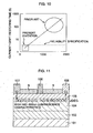
- Fig. 11 illustrates an example of the configuration of a previously-proposed GaN-HEMT.
- an AlN layer 102 and a GaN layer 103 are laminated in order, for example, on a SiC substrate 101 to form a buffer layer. Further, an n-type AlGaN layer 105 is laminated on the GaN layer 103.
- a gate electrode 106 which is Schottky-connected to the AlGaN layer 105, and a source electrode 107 and a drain electrode 108 which are spaced apart from the both sides of the gate electrode 106 on the AlGaN layer 105 and are ohmic-connected thereto are formed by pattern formation.
- a SiN layer 9 as a protective insulating film is laminated between the source electrode 107 and the drain electrode 108 on the AlGaN layer 105.
- a GaN-HEMT is configured.
- Fig. 12 illustrates the relationship between the time and the output value when a previously-proposed GaN-HEMT is continuously used.
- the output value thereof is decreased to about 70 % of the initial value after continuous use thereof, for example, for 15 years.
- the reduction of the output value by about 30 % after a lapse of 15 years can not be said to be sufficiently practical, and thus previously-proposed GaN-HEMTs can be considered to have a significant problem in this regard.
- US 2003/0201459 A1 relates to high electron mobility transistor (HEMT) that includes a semi-insulating silicon carbide substrate, an aluminum nitride buffer layer on the substrate, an insulating gallium nitride layer on the buffer layer, an active structure of aluminum gallium nitride on the gallium nitride layer, a passivation layer on the aluminum gallium nitride active structure, and respective source, drain and gate contacts to the aluminum gallium nitride active structure.
- HEMT high electron mobility transistor
- US 2004/0195562 A1 relates to a device having a substrate, a buffer region positioned upon the substrate, wherein the buffer region has an upper buffer region and a lower buffer region, a heterojunction region positioned upon the buffer region, and a superlattice positioned between the lower buffer region and the upper buffer region, wherein the device is configured to function as a heterojunction field effect transistor.
- WO 02/48434 A2 relates to semiconductor materials including a gallium nitride material layer formed on a silicon substrate and methods to form the semiconductor materials.
- the semiconductor materials include a transition layer formed between the silicon substrate and the gallium nitride material layer.
- the transition layer is compositionally-graded with the aim of lowering stress in the gallium nitride material layer which can result from differences in thermal expansion rates between the gallium nitride material and the substrate.
- the lowering of stresses in the gallium nitride material layer may reduce the tendency of cracks to form.
- the buffer layer is formed by forming a third layer containing an AlGaN layer between the first layer and the second, buffer layer.
- the present inventors focused attention on the phenomenon of output drift during power-operation of a GaN-HEMT, in order to easily grasp, in a short time, changes in the characteristics of a GaN-HEMT which appear as degradation of output value with a lapse of time. Such changes become prominent at the instant of turning off the power-operation of a GaN-HEMT in particular.
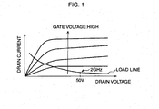
- Fig. 1 illustrates the current-voltage characteristic curve of a GaN-HEMT.
- the horizontal axis represents the drain (drain-source) voltage and the vertical axis represents the drain (drain-source) current.
- the drain voltage is about 50V. Therefore, the drain voltage is set to 50V and a high-frequency signal at 2 GHz, for example, is input to the GaN-HEMT (the power operation is turned on) for flowing a slight drain current. In this case, the output of the GaN-HEMT changes so as to draw a curve (a load line) as illustrated.
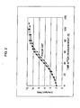
- Fig. 2 illustrates monitored slight drain currents which flowed at the instant of turning off the power-operation of a conventional GaN-HEMT.
- the horizontal axis represents the measuring time (second) and the vertical axis represents the drain current value (bias-point current: mA/mm) at the instant of turning off the power-operation of the GaN-HEMT.
- the number of measurements was three.
- 2-dimension electron gas (2DEG) moves through the GaN layer 104 as an electron transit layer between the source electrode 107 and the drain electrode 108, and this movement causes predetermined outputs.
- the present invention utilizes the so-called photoluminescence measurement method as the method for quantitatively estimating whether the amount of 2-dimension electron gas is large or small, and particularly focuses attention on the light-emission intensity in the 500-600 nm band.
- the photoluminescence measurement method is a procedure which applies short-wavelength light to the surface of the AlGaN layer 105 in a detection sample in which the AlGaN layer 105 has been formed, namely the gate electrode 106, etc., has not been formed, and then measures intensity of light emitted from the detection sample.
- Fig. 3 is a characteristic view illustrating the relationship between the light-emission wavelength and the light-emission intensity obtained by the photoluminescence measurement method, when a previously-proposed GaN-HEMT (the AlGaN layer and the GaN layer thereof) was used as the detection sample.
- the horizontal axis represents the light-emission wavelength (nm) and the vertical axis represents the light-emission intensity (relative value). Further, there is shown some noise in Fig. 3 .
- light-emission intensities for light-emission wavelengths of the applied light are defined by their energy levels.
- 2-dimension electron gas is captured in traps in the GaN layer, this will cause light emission at light-emission intensities different from the defined light-emission intensities.
- the GaN layer including a large amount of Ga holes and carbon, there are formed traps called as deep energy levels.
- the carbon is generally included in the methyl group of the Ga material for the GaN layer.
- a GaN layer containing a large amount of Ga holes and carbon generates a high light-emission intensity in the 500-600 nm band (so-called yellow luminescence), based on the relation with the band gap of GaN, because of the aforementioned traps, as illustrated in Fig. 3 .
- the detection sample used for the photoluminescence measurement in Fig. 3 exhibited a Ga-hole concentration of 3 ⁇ 10 18 /cm 3 and a carbon concentration of 2 ⁇ 10 18 /cm 3 , both of which were large values.
- the present inventor has studied about the relationship between the light-emission peak intensity (relative value) in the 500-600 nm band and the current-drift restoring time (second) and has found that there is approximately a proportional relationship therebetween, as illustrated in Fig. 4 .
- a light-emission peak intensity in the 500-600 nm band which corresponds to the restoring time satisfying the aforementioned reliability specification was converted into a value relating to the light-emission intensity at the GaN-band edge which exhibits substantially a constant value regardless of the amount of contained Ga holes and carbon.
- the A/B ratio was about 0.2, where "A" is the maximum light-emission intensity value in the 500-600 nm band, and "B” is the light-emission intensity at the GaN band-edge. Therefore, it is desirable to employ a GaN layer which exhibits A/B ratio described above of 0.2 or less, as the electron transit layer in the GaN-HEMT.
- the excitation condition for the photoluminescence measurement was an excitation condition adjusted to maximize the light emission in the 500 nm range under weak excitation conditions and was not a strong excitation condition such as those for use in laser diode measurements.
- the amount of contained Ga holes and carbon can be adjusted. More specifically, the amount of Ga holes can be adjusted to a value within the range of 1 ⁇ 10 12 /cm 3 to 1 ⁇ 10 18 /cm 3 and the carbon concentration can be adjusted to a value within the range of 1 ⁇ 10 13 /cm 3 to 1 ⁇ 10 18 /cm 3 .
- the upper limit value for the amount of Ga holes (1 ⁇ 10 18 /cm 3 ) and the upper limit value for carbon (1 ⁇ 10 18 /cm 3 ) were determined for the reason that greater amounts of Ga holes and carbon than these values will increase the light-emission intensity in the 500-600 nm band, thus preventing the aforementioned ratio condition from being satisfied.
- the lower limit value for the amounts of Ga holes (1 ⁇ 10 12 /cm 3 ) and the lower limit value for carbon (1 ⁇ 10 13 /cm 3 ) are determined for the reason that the amounts of Ga holes and carbon will unavoidably become higher than these values, due to factors caused by Ga material, etc.
- the Ga material is reduced and the growing rate of the GaN is decreased while the high resistivity of the GaN is maintained, since the amount of Ga holes can be decreased when the carbon concentration is decreased, in considering that carbon is included in the methyl group in the Ga material as previously described.
- the growing rate of the GaN is preferably within the range of 0.1 nm/second to 1 nm/second. If the growing rate is greater than 1 nm/second, the carbon concentration can not be sufficiently reduced. Growing rates lower than 0.1 nm/second will induce a problem in terms of the mass productivity.
- the molar ratio of the N material which is, for example, NH 3 to the Ga material (the number of of moles of N/ the number of moles of Ga), so-called a V/III ratio, is set to a value within the range of 10000 to 100000. If the V/III ratio is lower than 10000, the carbon concentration can not be sufficiently reduced.
- the V/III ratio is higher than 100000, this will cause a problem of difficulty in the treatment of NH 3 after use.
- the A/B ratio can be controlled to about 0.2 or less, thereby enabling significant reduction in the current-drift restoring time.
- the present inventor has found that traps for 2-dimension electron gas are formed in the AlN layer which is grown directly on the substrate. Namely, when the AlN layer has a large thickness greater than 100 nm, for example, or a high oxygen concentration higher than 1 ⁇ 10 19 /cm 3 , for example, there will be formed traps in the AlN layer. This is because oxygen is easily bound to Al and the Al material contains oxygen.
- the lower limit for the thickness of the AlN layer is set to 10 nm for the reason that excessively small thicknesses of the AlN layer will prevent the AlN layer from being a flat film since AlN grows laterally at first as will be described later.
- the lower limit for the oxygen concentration in the AlN layer is set to 1 ⁇ 10 13 /cm 3 since excessively low oxygen concentrations cause traps to be formed in the AlN layer. From the above consideration, the present invention controls the thickness of the AlN layer to a value within the range of 10 nm to 100 nm and also controls the oxygen concentration in the AlN layer to a value within the range of 1 ⁇ 10 13 /cm 3 to 1 ⁇ 10 19 /cm 3 .
- Fig. 5 illustrates the relationship between the amount (%) of Ga within the AlN layer and the amount (/cm 3 ) of traps within the AlN layer.
- the amount of Ga which causes the amount of traps to be the permissible maximum amount illustrated by the dot line increases with increasing thickness of the AlN layer.
- the oxygen concentration within the AlN layer is to be controlled to a value within the range of 1 ⁇ 10 13 /cm 3 to 1 ⁇ 10 19 /cm 3 and that the thickness of the AlN layer is to be controlled to a value within the range of 10 nm to 100 nm
- Ga is interfused in the AlN layer with a concentration within the range of 1 % to 80 %.
- the N material which is, for example, NH 3 , includes a large amount of Si.
- a SiC coating is applied to susceptors for holding a wafer used as the substrate. Therefore, during the growth of the GaN layer, Si will be unavoidably interfused therein. In the case of using a MOVPE process for growing and forming the AlN layer and the GaN layer, these layers will grow laterally at first and then will grow upwardly after some amount of thickness is accumulated. During the phase of the lateral growth, Si contained in the N material and Si contained in the SiC coating on the susceptors will be interfused therein and, after some amount of thickness has been accumulated, they will be hardly interfused therein.
- Si will be introduced to lower portions of the respective layers during the initial growth and formation phases of the respective layers.
- the present invention utilizes that Al incorporated in the GaN layer alleviates interfusion of Si therein, in addition to that Si is introduced to lower portions of the respective layers during the initial growth phases.
- an AlGaN layer including a small amount of Al as, so to say, an initial layer of the GaN layer, is formed on the AlN layer, and then the GaN layer as the electron transit layer is subsequently formed on the AlGaN layer. This can significantly reduce Si introduced into the GaN layer, thereby providing a non-doped GaN layer with high resistivity.
- the AlGaN layer which has been formed has a Si concentration within the range of 1 ⁇ 10 13 /cm 3 to 1 ⁇ 10 16 /cm 3 . If the Si concentration is higher than 1 ⁇ 10 16 /cm 3 , there is not provided the effect of alleviating interfusion of Si. It is considered impossible to cause the Si concentration to be lower than 1 ⁇ 10 13 /cm 3 , because of factors caused by the N material, etc., and the limitations of measurements.
- the thickness of the AlGaN layer is an important factor of suppression of Si interfused in the GaN layer.
- the AlGaN layer is formed to a thickness within the range of 10 nm to 200 nm. If the thickness is smaller than 10 nm, the layer will not be a flat film. If the thickness is greater than 200 nm, traps will be formed in the film.
- the growing temperature during the formation of the GaN layer is set to a low temperature, and, in this case, to a value within the range of from 1000 °C to 1100 °C. If the growing temperature is set to a value lower than 1000 °C, this will lead to increase in the carbon concentration within the GaN layer. If the growing temperature is set to a value higher than 1100 °C, this will facilitate interfusion of Si. At this time, it is preferable to define the growing pressure, as well as the growing temperature, during the formation of the GaN layer.
- the growing pressure in order to aid the low growing temperature, it is preferable to set the growing pressure to a value within the range of from 6.7 ⁇ 10 3 Pa (50 torr) to 4.0 ⁇ 10 4 Pa (300 torr). It is not realistic to set the growing pressure to below 6.7 ⁇ 10 3 Pa, while growing pressures higher than 4.0 ⁇ 10 4 Pa hinder temperature reduction in the growing.
- Fig. 6 is a schematic cross sectional view illustrating the configuration of the GaN-HEMT according to the present embodiment.
- a buffer layer 11 including an electron transit layer, an AlGaN layer 13 serving as an electron supply layer and an n-type GaN layer 10 are laminated on a substrate formed from sapphire, SiC, GaN, Si, etc., and, in this case, a SiC substrate 1.
- a gate electrode 6 is formed with pattern formation on the GaN layer 10.
- a source electrode 7 and a drain electrode 8 are formed with pattern formation such that they are spaced apart from the both sides of the gate electrode 6.
- a SiN layer 9, as a protective insulating film, is laminated between the source electrode 7 and the drain electrode 8 on the n-type GaN layer 10, and thus the GaN-HEMT is configured.
- the buffer layer 11 is configured by continuously laminating and growing an AlN layer 2, an AlGaN layer 3 and a GaN layer 4.
- the AlN layer 2 has a thickness within the range of 10 nm to 100 nm and, in this case, a thickness of about 20 nm and the oxygen concentration thereof is held within the range of 1 ⁇ 10 13 /cm 3 to 1 ⁇ 10 19 /cm 3 .
- Ga may be interfused in the AlN layer 2 with a ratio within the range of 1 % to 80 %, and, for example, a ratio of about 50 %. This may decrease the oxygen concentration to, for example, about 1 ⁇ 10 18 /cm 3 , and may further improve the current-drift restoring time.
- the AlGaN layer 3 is provided in order to suppress interfusion of Si in the GaN layer 4 during the growth of the GaN layer 4.
- the AlGaN layer 3 has a thickness within the range of 10 nm to 200 nm and, in this case, has a thickness of about 30 nm. Further, the AlGaN layer 3 has a Si concentration below 1 ⁇ 10 16 /cm 3 , and in this case, has a Si concentration of about (5 ⁇ 10 14 )/cm 3 .
- the AlGaN layer 3 is intended to have a low Al-composition ratio and, in Al x Ga (1-x) N, x is of a value of 0 ⁇ x ⁇ 0.3 and, for example, x is 0.05.
- Al in the AlGaN layer 3 will suppress interfusion of Si during the lateral growth of the AlGaN.
- an AlGaInN layer may be formed instead of the AlGaN layer 3.
- an AlGaInN layer including In there will be provided an effect of suppressing interfusion of Si.
- x is of a value of 0 ⁇ x ⁇ 0.3
- y is of a value of 0 ⁇ y ⁇ 0.1, for example.
- the GaN layer 4 functions as an electron transit layer and is formed such that, at least at one portion thereof, the A/B ratio becomes 0.2 or less obtained by photoluminescence measurement, where "A" is the maximum light-emission intensity value in the 500-600 nm band, and "B” is the light-emission intensity at the GaN band-edge. In this case for example, it is about 0.16.
- the excitation condition for the photoluminescence measurement is an excitation condition adjusted to maximize the light emission in the 500 nm range in weak excitation conditions and is not a strong excitation condition such as those used for laser diode measurements.
- the thickness of the GaN layer 4 is set to a value within the range of 500 nm to 5000 nm, and, in this case, to about 1000 nm.
- the current-drift restoring time shows a value which sufficiently satisfies the aforementioned reliability specification. This is because the amount of Ga holes and the carbon concentration are held to low values. More specifically, the amount of Ga holes in the GaN layer 4 is held within the range of 1 ⁇ 10 12 /cm 3 to 1 ⁇ 10 18 /cm 3 , and, for example, at a value of 1 ⁇ 10 14 /cm 3 .
- the carbon concentration thereof is held within the range of 1 ⁇ 10 13 /cm 3 to 1 ⁇ 10 18 /cm 3 and, for example, at a value of 2 ⁇ 10 14 /cm 3 . Further, the Si concentration of the GaN layer 4 is held at a low value of, for example, 1 ⁇ 10 14 /cm 3 .
- the AlGaN layer 13 functions as an electron supply layer and is configured by laminating a non-doped AlGaN layer 12 with a thickness of about 3 nm and an n-type AlGaN layer 5 with a thickness of about 20 nm.
- the n-type AlGaN layer 5 is formed by doping with Si to a concentration of, for example, about 4 ⁇ 10 18 /cm 3 .
- the n-type GaN layer 10 is for suppressing changes in the on-resistance during operation, called as current collapse, and is formed by doping with Si to a concentration of, for example, about 5 ⁇ 10 18 /cm 3 .
- the gate electrode 6 is formed by laminating Ni/Au in order and is Schottky-connected to the n-type GaN layer 10.
- the source electrode 7 and the drain electrode 8 are formed by laminating Ti/Al in order, and are ohmic-connected to exposed portions of the surface of the n-type AlGaN layer 5 from which the n-type GaN layer 10 has been removed such that they are spaced apart from the right and left sides of the gate electrode 6.
- the SiN layer 9 is a protective insulating film formed between the gate electrode 6 and the source electrode 7 and between the gate electrode 6 and the drain electrode 8 and has a function of suppressing current collapse in cooperation with the n-type GaN layer 10.
- the GaN-HEMT With the GaN-HEMT according to the present embodiment, by controlling the gate voltage applied to the gate electrode 6, 2-dimension electron gas moves between the source electrode 7 and the drain electrode 8 through the GaN layer 4 as the electron transit layer, and this movement generates predetermined outputs.
- the GaN-HEMT according to the present embodiment traps will be hardly formed in the AlN layer 2, etc., as well as in the GaN layer 4, and therefore 2-dimension electron gas beneath the gate electrode 6 will not be decreased.
- the current-drift restoring time can be shortened to below the reliability specification, thereby holding the degradation with a lapse of time of the output value to 5 % or less of the initial value after continuous use for 15 years.
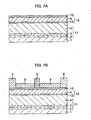
- Figs. 7A and 7B are schematic cross sectional views illustrating the fabricating method of the GaN-HEMT according to the present embodiment, in order of the process steps.
- a SiC substrate 1 is prepared and, on the SiC substrate 1, an AlN layer 2, an AlGaN layer 3 and a GaN layer 4 constituting a buffer layer 11, a non-doped AlGaN layer 12 and an n-type AlGaN layer 5 constituting an AlGaN layer 13, and an n-type GaN layer 10 are continuously grown and formed in order, with MOVPE processes.
- the method for growing these layers is not limited to MOVPE processes and may be, for example, MBE processes.
- the growing rate, the V/III ratio, the growing temperature, and the growing pressure for the GaN layer 4 are adjusted.
- the former two, or the growing rate and the V/III ratio are conditions for satisfying Requirement 1 of holding the aforementioned A/B ratio obtained from photoluminescence measurements to 0.2 or less and, therefore, shortening the current-drift restoring time, thereby reducing the degradation with a lapse of time of the GaN-HEMT.
- the latter two, or the growing temperature and the growing pressure are conditions for satisfying Requirement 2 of suppressing increases of interfusion of Si, which would occur only by setting the aforementioned former two conditions.
- the growing rate is set to a low value within the range of 0.1 nm/second to 1 nm/second, and, in this case, to 0.5 nm/second.
- the V/III ratio is set to a high value within the range of 10000 to 100000 and, in this case, to about 80000.
- the growing temperature is set to a low temperature within the range of from 1000 °C to below 1100 °C and, in this case, to 1045 °C.
- the growing pressure is set to a low pressure within the range of from 6.7 ⁇ 10 3 Pa (50 torr) to 4.0 ⁇ 10 4 Pa (300 torr) and, in this case, to 1.3 ⁇ 10 4 Pa (100 torr).
- the gate electrode 6, the source electrode 7, the drain electrode 8 and the SiN layer 9 are formed respectively.
- the source electrode 7 and the drain electrode 8 are formed by pattern formation.
- the portions of the n-type GaN layer 10 at which the source electrode 7 and the drain electrode 8 are to be formed are removed to expose the surface of the N-type AlGaN layer 5 corresponding to the aforementioned portions.
- the Ti/Al is subjected to an annealing process at 550 °C for 30 seconds to alloy the Ti/Al.
- the source electrode 7 and the drain electrode 8 are formed.
- the gate electrode 6 is formed through pattern formation.
- Ni with a thickness of about 30 nm and Au with a thickness of about 400 nm are laminated in order, and then, by lithography and subsequent dry etching, the Ni/Al is patterned into an electrode shape to form the gate electrode 6.
- SiN is deposited to a film thickness which will not bury the gate electrode 6, the source electrode 7 and the drain electrode 8 and, in this case, to a thickness of about 40 nm, to form the SiN layer 9.
- the SiN on the gate electrode 6, the source electrode 7 and the drain electrode 8 may be removed.
- the element separation is achieved by predetermined ion implantation.
- experiment (Experiment 1) for demonstrating the superiority of the present embodiment over conventional arts in terms of the current-drift restoring time and experiment (Experiment 2) for demonstrating the effect of suppressing interfusion of Si of the GaN-HEMT according to the present embodiment were performed.
- Fig. 8 illustrates monitored drain currents flowed at the instant of turning off the power-operation, in the GaN-HEMT according to the present embodiment.
- the horizontal axis represents the measuring time (second) and the vertical axis represents the drain current value (bias-point current: mA/mm) at the instant of turning off the power-operation of the GaN-HEMT.
- the number of measurements was three.
- Fig. 8 there are also illustrated the results of measurements for the previously-proposed GaN-HEMT of Fig. 2 .
- the amount of Ga holes and the carbon concentration in the GaN layer serving as the electron transit layer were high values of 3 ⁇ 10 18 /cm 3 and 2 ⁇ 10 18 /cm 3 , respectively
- the amount of Ga holes and the carbon concentration in the GaN layer serving as the electron transit layer, in the GaN-HEMT according to the present embodiment were 1 ⁇ 10 14 /cm 3 and 2 ⁇ 10 14 /cm 3 , respectively, and these values are both lower compared with those of the previously-proposed GaN-HEMT.
- the bias-point current decreased to about 10 % of the value before the power-operation and it took over one minute to restore that.
- the bias-point current decreased to about 60 % of the value before the power-operation and was restored in a short time interval of about 10 seconds.
- Fig. 9 is a characteristic view illustrating the relationship between the light-emission wavelength and the light-emission intensity in the case of using the GaN-HEMT (the AlGaN layer and the GaN layer therein) according to the present embodiment as the detection sample, which was obtained by photoluminescence measurements.
- Fig. 9 corresponds to Fig. 3 for the previously-proposed GaN-HEMT (the AlGaN layer and the GaN layer therein) used as the detection sample.
- the horizontal axis represents the light-emission wavelength (nm) and the vertical axis represents the light-emission intensity (relative value). Further, there is also illustrated some noise in Fig. 9 .
- the GaN-HEMT according to the present embodiment generated the maximum light-emission intensity value in the 500-600 nm band which was about one-eighth the light-emission intensity in the 500-600 nm band generated from the previously-proposed GaN-HEMT, and there were also obtained other results of experiments which showed that this ratio was about one-tenth.
- the A/B ratio is a high value of about 1.2, where "A" is the maximum light-emission intensity value in the 500-600 nm band, and "B" is the light-emission intensity at the GaN band-edge.
- the aforementioned A/B ratio is 0.2 or less and, in this case, about 0.16.
- the excitation condition for the photoluminescence measurement was an excitation condition adjusted to maximize the light emission in the 500 nm range in weak excitation conditions and was not a strong excitation condition such as those used for laser diode measurements.
- the extremely-short current-drift restoring time of the GaN-HEMT according to the present embodiment is indicated from a low light-emission peak intensity in the 500-600 nm band.
- Fig. 10 illustrates the relationship between the light-emission peak intensity (relative value) in the 500-600 nm band and the current-drift restoring time (second), for the GaN-HEMT according to the present embodiment, based on comparison with the previously-proposed GaN-HEMT.
- Fig. 10 corresponds to Fig. 4 .
- the GaN-HEMT according to the present embodiment exhibits a short restoring time which sufficiently satisfies the reliability specification.
- the GaN-HEMT (the AlGaN layer and the GaN layer therein) according to the present embodiment, element separation characteristics were inspected and, as a result, there was found no problem.
- the GaN layer serving as the electron transit layer was formed at a growing temperature of 1100 °C.
- the Si concentration in the GaN layer became a high value of 2 ⁇ 10 16 /cm 3 and thus the element separation characteristics was degraded by four orders of magnitude as compared with that of the present embodiment, and the FET characteristics exhibited no pinch-off. Therefore, it was found that, in order to hold the Si concentration of the GaN layer at a low value, it is necessary to set the growing temperature to below 1100 °C.
- GaN-HEMT which exhibits extremely small variations in the characteristics and small degradation with a lapse of time.
- This GaN-HEMT can provide highly reliable characteristics required for amplifiers for portable-phone base-stations and provides significant effects of contributing to development in the market for electronic devices employing GaN.
- a highly reliable compound semiconductor device which exhibits extremely small variations in the characteristics and small degradation with a lapse of time.
- This compound semiconductor device can provide highly reliable characteristics required for base-station amplifiers for portable-phone and provides a significant effect of contributing to development in the market for electronic devices using GaN.
Landscapes
- Engineering & Computer Science (AREA)
- Microelectronics & Electronic Packaging (AREA)
- Power Engineering (AREA)
- Physics & Mathematics (AREA)
- Condensed Matter Physics & Semiconductors (AREA)
- General Physics & Mathematics (AREA)
- Computer Hardware Design (AREA)
- Manufacturing & Machinery (AREA)
- Chemical & Material Sciences (AREA)
- Materials Engineering (AREA)
- Ceramic Engineering (AREA)
- Junction Field-Effect Transistors (AREA)
Claims (18)
- Verbindunghalbleitervorrichtung, aufweisend eine Transistorkonfiguration, umfassend:ein Substrat (1);eine Pufferschicht (11), ausgebildet auf dem Substrat; undeine Elektronenversorgungsschicht (13), enthaltend AlGaN, ausgebildet auf der Pufferschicht;wobei die Pufferschicht eine AlN enthaltende erste Schicht (2) und eine GaN enthaltende zweite Schicht (4) umfasst;dadurch gekennzeichnet, dass die Menge von Ga-Löchern innerhalb des Bereichs von 1×10¹²/cm3 bis 1×10¹⁴/cm3 und die Kohlenstoffkonzentration innerhalb des Bereichs von 1×10¹³/cm3 ist 2×10¹⁴/cm3 in der zweiten Schicht (4) ist und darin, dassdie zweite Schicht, zumindest ein Teil davon, ein A/B-Verhältnis von 0,2 oder weniger aufweist, welches durch eine Photolumineszenzmessung erhalten wird, wobei "A" der maximale Gelb-Lumineszenz-Intensitätswert in dem 500-600 nm Band einer Lichtemissionswellenlänge ist und "B" die Lichtemissionsintensität an der GaN-Bandkante ist.
- Verbundhalbleitervorrichtung gemäß Anspruch 1,
wobei die Pufferschicht (11) durch Laminieren der ersten Schicht (2), der zweiten Schicht (4) und einer dritten Schicht (3), enthaltend AlGaN, vorgesehen zwischen der ersten Schicht und der zweiten Schicht, ausgebildet ist. - Verbundhalbleitervorrichtung gemäß Anspruch 2, wobei die dritte Schicht (3) Al×Ga(1-x)N umfasst, wobei x ein Wert von 0<x<0,3 ist.
- Verbundhalbleitervorrichtung gemäß Anspruch 2 oder 3, wobei die erste Schicht (2) eine Dicke innerhalb des Bereichs von 10 nm bis 100 nm aufweist.
- Verbundhalbleitervorrichtung gemäß einem der vorstehenden Ansprüche, wobei die Ga-Konzentration in der ersten Schicht (2) innerhalb des Bereichs von 1% bis 80% ist.
- Verbundhalbleitervorrichtung gemäß einem der vorstehenden Ansprüche wobei die Sauerstoff-Konzentration in der ersten Schicht (2) innerhalb des Bereichs von 1×10¹³/cm3 bis 1×10¹⁹/cm3 ist.
- Verbundhalbleitervorrichtung gemäß einem der Ansprüche 2 bis 4, wobei die dritte Schicht (3) eine Dicke innerhalb des Bereichs von 10 nm bis 200 nm aufweist.
- Verbundhalbleitervorrichtung gemäß einem der Ansprüche 2 bis 4 oder Anspruch 7, wobei die Silizium-Konzentration in der dritten Schicht (3) gleich oder geringer als 1×10¹⁶/cm3 ist.
- Fabrikationsverfahren einer Verbundhalbleitervorrichtung, umfassend die Schritte:Ausbilden einer Pufferschicht (11) auf einem Substrat (1); undAusbilden einer Elektronenversorgungsschicht (13), umfassend AlGaN, auf der Pufferschicht;wobeidie Pufferschicht durch kontinuierliches Laminieren einer AlN umfassenden ersten Schicht (2) und einer GaN umfassenden zweiten Schicht in dieser Reihenfolge ausgebildet wird; undwenn die zweite Schicht ausgebildet wird, die Wachstumsrate auf einen Wert innerhalb eines Bereichs von 0,1 nm/Sekunde bis 1 nm/Sekunde eingestellt ist und das modulare Verhältnis von N zu Ga auf einen Wert innerhalb des Bereichs von 10.000 bis 100.000 eingestellt ist,dadurch gekennzeichnet, dass die Menge von Ga-Löchern innerhalb des Bereichs von 1×10¹²/cm3 bis 1×10¹⁴/cm3 und die Kohlenstoffkonzentration innerhalb des Bereichs von 1×10¹³/cm3 ist 2×10¹⁴/cm3 in der zweiten Schicht (4) ist und darin, dassdie zweite Schicht, zumindest ein Teil davon, ein A/B-Verhältnis von 0,2 oder weniger aufweist, welches durch eine Photolumineszenzmessung erhalten wird, wobei "A" der maximale Gelb-Lumineszenz-Intensitätswert in dem 500-600 nm Band einer Lichtemissionswellenlänge ist und "B" die Lichtemissionsintensität an der GaN-Bandkante ist.
- Fabrikationsverfahren einer Verbundhalbleitervorrichtung gemäß Anspruch 9, wobei die Pufferschicht (11) durch Ausbilden einer dritten Schicht (3), umfassend AlGaN, vorgesehen zwischen der ersten Schicht (2) und der zweiten Schicht (4) ausgebildet wird.
- Verbundhalbleitervorrichtung gemäß Anspruch 10, wobei die dritte Schicht (3) Al×Ga(1-x)N umfasst, wobei x der Wert von 0<x<0,3 ist.
- Fabrikationsverfahren einer Verbundhalbleitervorrichtung gemäß Anspruch 10 oder 11, wobei die Wachstumstemperatur auf einen Niederwert innerhalb des Bereichs von 1000°C bis weniger als 1100°C eingestellt wird, wenn die dritte Schicht (3) ausgebildet wird.
- Fabrikationsverfahren einer Verbundhalbleitervorrichtung gemäß Anspruch 12, wobei der Wachstumsdruck auf einen Wert innerhalb eines Bereichs von 6,7×10³ Pa bis 4,0×10⁴ Pa eingestellt wird, wenn die zweite Schicht (4) ausgebildet wird.
- Fabrikationsverfahren einer Verbundhalbleitervorrichtung gemäß einem der Ansprüche 9 bis 13, wobei die erste Schicht (2) eine Dicke innerhalb des Bereichs von 10 nm bis 100 nm aufweist.
- Fabrikationsverfahren einer Verbundhalbleitervorrichtung gemäß einem der Ansprüche 9 bis 14, wobei die Ga-Konzentration in der ersten Schicht (2) innerhalb des Bereichs von 1% bis 80% ist.
- Fabrikationsverfahren einer Verbundhalbleitervorrichtung gemäß einem der Ansprüche 9 bis 15, wobei die Sauerstoff-Konzentration in der ersten Schicht (2) innerhalb des Bereichs von 1×10¹³/cm3 bis 1×10¹⁹/cm3 ist.
- Fabrikationsverfahren einer Verbundhalbleitervorrichtung gemäß einem der Ansprüche 9 bis 16, wobei die dritte Schicht (3) eine Dicke innerhalb des Bereichs von 10 nm bis 200 nm aufweist.
- Fabrikationsverfahren einer Verbundhalbleitervorrichtung gemäß einem der Ansprüche 9 bis 17, wobei die Silizium-Konzentration in der dritten Schicht (3) gleich oder geringer als 1×10¹⁶/cm3 ist.
Applications Claiming Priority (1)
| Application Number | Priority Date | Filing Date | Title |
|---|---|---|---|
| JP2004332284A JP4514584B2 (ja) | 2004-11-16 | 2004-11-16 | 化合物半導体装置及びその製造方法 |
Publications (3)
| Publication Number | Publication Date |
|---|---|
| EP1657754A2 EP1657754A2 (de) | 2006-05-17 |
| EP1657754A3 EP1657754A3 (de) | 2009-04-08 |
| EP1657754B1 true EP1657754B1 (de) | 2015-09-30 |
Family
ID=35610146
Family Applications (1)
| Application Number | Title | Priority Date | Filing Date |
|---|---|---|---|
| EP05254240.4A Active EP1657754B1 (de) | 2004-11-16 | 2005-07-06 | Verbindungshalbleiteranordnung und Verfahren zur Herstellung |
Country Status (3)
| Country | Link |
|---|---|
| US (2) | US7638819B2 (de) |
| EP (1) | EP1657754B1 (de) |
| JP (1) | JP4514584B2 (de) |
Families Citing this family (39)
| Publication number | Priority date | Publication date | Assignee | Title |
|---|---|---|---|---|
| US9524869B2 (en) * | 2004-03-11 | 2016-12-20 | Epistar Corporation | Nitride-based semiconductor light-emitting device |
| KR100674829B1 (ko) * | 2004-10-29 | 2007-01-25 | 삼성전기주식회사 | 질화물계 반도체 장치 및 그 제조 방법 |
| JP4792814B2 (ja) * | 2005-05-26 | 2011-10-12 | 住友電気工業株式会社 | 高電子移動度トランジスタ、電界効果トランジスタ、エピタキシャル基板、エピタキシャル基板を作製する方法およびiii族窒化物系トランジスタを作製する方法 |
| JP2007335736A (ja) * | 2006-06-16 | 2007-12-27 | New Japan Radio Co Ltd | 窒化物半導体装置 |
| RU2326993C2 (ru) * | 2006-07-25 | 2008-06-20 | Самсунг Электро-Меканикс Ко., Лтд. | Способ выращивания монокристалла нитрида на кремниевой пластине, нитридный полупроводниковый светоизлучающий диод, изготовленный с его использованием, и способ такого изготовления |
| JP4531071B2 (ja) | 2007-02-20 | 2010-08-25 | 富士通株式会社 | 化合物半導体装置 |
| US20090321787A1 (en) * | 2007-03-20 | 2009-12-31 | Velox Semiconductor Corporation | High voltage GaN-based heterojunction transistor structure and method of forming same |
| JP5095253B2 (ja) | 2007-03-30 | 2012-12-12 | 富士通株式会社 | 半導体エピタキシャル基板、化合物半導体装置、およびそれらの製造方法 |
| JP2008277655A (ja) * | 2007-05-02 | 2008-11-13 | Hitachi Cable Ltd | 半導体エピタキシャルウェハ及び電界効果トランジスタ |
| JP4584293B2 (ja) | 2007-08-31 | 2010-11-17 | 富士通株式会社 | 窒化物半導体装置、ドハティ増幅器、ドレイン電圧制御増幅器 |
| US8222041B2 (en) * | 2008-05-09 | 2012-07-17 | University Of Florida Research Foundation, Inc. | Oxygen and carbon dioxide sensing |
| CN101604704B (zh) * | 2008-06-13 | 2012-09-05 | 西安能讯微电子有限公司 | Hemt器件及其制造方法 |
| JP4677499B2 (ja) * | 2008-12-15 | 2011-04-27 | Dowaエレクトロニクス株式会社 | 電子デバイス用エピタキシャル基板およびその製造方法 |
| JP5607548B2 (ja) | 2009-01-21 | 2014-10-15 | 日本碍子株式会社 | 3b族窒化物結晶板製造装置 |
| JP5487631B2 (ja) | 2009-02-04 | 2014-05-07 | 富士通株式会社 | 化合物半導体装置及びその製造方法 |
| JP5401145B2 (ja) * | 2009-03-26 | 2014-01-29 | 株式会社トクヤマ | Iii族窒化物積層体の製造方法 |
| JP2011035065A (ja) * | 2009-07-30 | 2011-02-17 | Hitachi Cable Ltd | 半導体装置 |
| JP5188545B2 (ja) * | 2009-09-14 | 2013-04-24 | コバレントマテリアル株式会社 | 化合物半導体基板 |
| JP2011166067A (ja) * | 2010-02-15 | 2011-08-25 | Panasonic Corp | 窒化物半導体装置 |
| JP6024075B2 (ja) * | 2010-07-30 | 2016-11-09 | 住友電気工業株式会社 | 半導体装置およびその製造方法 |
| JP5649112B2 (ja) | 2010-07-30 | 2015-01-07 | パナソニック株式会社 | 電界効果トランジスタ |
| JP5781292B2 (ja) * | 2010-11-16 | 2015-09-16 | ローム株式会社 | 窒化物半導体素子および窒化物半導体パッケージ |
| WO2013027722A1 (ja) | 2011-08-22 | 2013-02-28 | ルネサスエレクトロニクス株式会社 | 半導体装置 |
| JP6054620B2 (ja) * | 2012-03-29 | 2016-12-27 | トランスフォーム・ジャパン株式会社 | 化合物半導体装置及びその製造方法 |
| JP6087552B2 (ja) * | 2012-09-21 | 2017-03-01 | トランスフォーム・ジャパン株式会社 | 化合物半導体装置及びその製造方法 |
| JP6161246B2 (ja) | 2012-09-28 | 2017-07-12 | トランスフォーム・ジャパン株式会社 | 半導体装置及び半導体装置の製造方法 |
| US9812602B2 (en) * | 2012-12-20 | 2017-11-07 | Seoul Viosys Co., Ltd. | Light detection device |
| US9929310B2 (en) | 2013-03-14 | 2018-03-27 | Applied Materials, Inc. | Oxygen controlled PVD aluminum nitride buffer for gallium nitride-based optoelectronic and electronic devices |
| JP6128953B2 (ja) * | 2013-05-23 | 2017-05-17 | 三菱電機株式会社 | 増幅装置および増幅装置の制御方法 |
| JP6419418B2 (ja) * | 2013-05-29 | 2018-11-07 | 三菱電機株式会社 | 半導体装置 |
| GB2522407A (en) * | 2014-01-13 | 2015-07-29 | Seren Photonics Ltd | Semiconductor devices and fabrication methods |
| WO2016051935A1 (ja) | 2014-10-03 | 2016-04-07 | 日本碍子株式会社 | 半導体素子用のエピタキシャル基板およびその製造方法 |
| JP6030733B2 (ja) * | 2015-11-05 | 2016-11-24 | 住友化学株式会社 | トランジスタ用窒化物半導体エピタキシャルウエハ及び窒化物半導体電界効果トランジスタ |
| JP6696244B2 (ja) * | 2016-03-16 | 2020-05-20 | 住友電気工業株式会社 | 高電子移動度トランジスタ及び高電子移動度トランジスタの製造方法 |
| CN105590839B (zh) * | 2016-03-22 | 2018-09-14 | 安徽三安光电有限公司 | 氮化物底层、发光二极管及底层制备方法 |
| JP6233476B2 (ja) * | 2016-09-07 | 2017-11-22 | 富士通株式会社 | 化合物半導体装置 |
| TWI703726B (zh) * | 2016-09-19 | 2020-09-01 | 新世紀光電股份有限公司 | 含氮半導體元件 |
| JP7393138B2 (ja) * | 2019-06-24 | 2023-12-06 | 住友化学株式会社 | Iii族窒化物積層体 |
| CN113224154B (zh) | 2020-02-06 | 2023-08-08 | 联华电子股份有限公司 | 高电子迁移率晶体管及其制作方法 |
Family Cites Families (25)
| Publication number | Priority date | Publication date | Assignee | Title |
|---|---|---|---|---|
| JP3353527B2 (ja) * | 1995-03-24 | 2002-12-03 | 松下電器産業株式会社 | 窒化ガリウム系半導体の製造方法 |
| US5739554A (en) * | 1995-05-08 | 1998-04-14 | Cree Research, Inc. | Double heterojunction light emitting diode with gallium nitride active layer |
| JPH0964477A (ja) * | 1995-08-25 | 1997-03-07 | Toshiba Corp | 半導体発光素子及びその製造方法 |
| JP3604205B2 (ja) * | 1995-09-18 | 2004-12-22 | 日亜化学工業株式会社 | 窒化物半導体の成長方法 |
| JPH10294452A (ja) * | 1997-04-22 | 1998-11-04 | Sony Corp | ヘテロ接合電界効果トランジスタ |
| JPH10335637A (ja) * | 1997-05-30 | 1998-12-18 | Sony Corp | ヘテロ接合電界効果トランジスタ |
| JPH11204885A (ja) * | 1998-01-08 | 1999-07-30 | Sony Corp | 窒化物系iii−v族化合物半導体層の成長方法および半導体装置の製造方法 |
| JP2000068498A (ja) * | 1998-08-21 | 2000-03-03 | Nippon Telegr & Teleph Corp <Ntt> | 絶縁性窒化物膜およびそれを用いた半導体装置 |
| JP2000106365A (ja) | 1998-09-29 | 2000-04-11 | Matsushita Electric Ind Co Ltd | 半導体トランジスタ |
| US6614059B1 (en) * | 1999-01-07 | 2003-09-02 | Matsushita Electric Industrial Co., Ltd. | Semiconductor light-emitting device with quantum well |
| JP2000228535A (ja) * | 1999-02-08 | 2000-08-15 | Nippon Telegr & Teleph Corp <Ntt> | 半導体素子およびその製造方法 |
| JP4154558B2 (ja) * | 2000-09-01 | 2008-09-24 | 日本電気株式会社 | 半導体装置 |
| US6649287B2 (en) * | 2000-12-14 | 2003-11-18 | Nitronex Corporation | Gallium nitride materials and methods |
| US20030201459A1 (en) * | 2001-03-29 | 2003-10-30 | Sheppard Scott Thomas | Nitride based transistors on semi-insulating silicon carbide substrates |
| EP2267784B1 (de) * | 2001-07-24 | 2020-04-29 | Cree, Inc. | AlGaN/GaN HEMT MIT ISOLIERTEM GATE |
| JP2003209124A (ja) * | 2001-11-06 | 2003-07-25 | Sony Corp | 電界効果半導体素子の製造方法及び電界効果半導体素子 |
| US7030428B2 (en) * | 2001-12-03 | 2006-04-18 | Cree, Inc. | Strain balanced nitride heterojunction transistors |
| WO2003050849A2 (en) * | 2001-12-06 | 2003-06-19 | Hrl Laboratories, Llc | High power-low noise microwave gan heterojunction field effet transistor |
| US7112830B2 (en) * | 2002-11-25 | 2006-09-26 | Apa Enterprises, Inc. | Super lattice modification of overlying transistor |
| US7186302B2 (en) * | 2002-12-16 | 2007-03-06 | The Regents Of The University Of California | Fabrication of nonpolar indium gallium nitride thin films, heterostructures and devices by metalorganic chemical vapor deposition |
| JP4179539B2 (ja) * | 2003-01-15 | 2008-11-12 | 富士通株式会社 | 化合物半導体装置及びその製造方法 |
| KR20050117047A (ko) * | 2004-06-09 | 2005-12-14 | 삼성전자주식회사 | 주사각 확장 광학 시스템 및 이를 구비한 레이저 스캐닝장치 |
| US20060073621A1 (en) * | 2004-10-01 | 2006-04-06 | Palo Alto Research Center Incorporated | Group III-nitride based HEMT device with insulating GaN/AlGaN buffer layer |
| US7626217B2 (en) * | 2005-04-11 | 2009-12-01 | Cree, Inc. | Composite substrates of conductive and insulating or semi-insulating group III-nitrides for group III-nitride devices |
| US8575651B2 (en) * | 2005-04-11 | 2013-11-05 | Cree, Inc. | Devices having thick semi-insulating epitaxial gallium nitride layer |
-
2004
- 2004-11-16 JP JP2004332284A patent/JP4514584B2/ja active Active
-
2005
- 2005-07-06 EP EP05254240.4A patent/EP1657754B1/de active Active
- 2005-07-15 US US11/181,730 patent/US7638819B2/en active Active
-
2009
- 2009-11-05 US US12/591,031 patent/US7838903B2/en active Active
Also Published As
| Publication number | Publication date |
|---|---|
| US7838903B2 (en) | 2010-11-23 |
| EP1657754A3 (de) | 2009-04-08 |
| EP1657754A2 (de) | 2006-05-17 |
| US20060102926A1 (en) | 2006-05-18 |
| US20100051962A1 (en) | 2010-03-04 |
| JP4514584B2 (ja) | 2010-07-28 |
| JP2006147663A (ja) | 2006-06-08 |
| US7638819B2 (en) | 2009-12-29 |
Similar Documents
| Publication | Publication Date | Title |
|---|---|---|
| EP1657754B1 (de) | Verbindungshalbleiteranordnung und Verfahren zur Herstellung | |
| KR101497725B1 (ko) | 공핍형 GaN 기반 FET를 이용하는 캐스코드 회로 | |
| EP3413353B1 (de) | Im normalzustand abgeschalteter hemt-transistor mit selektiver erzeugung von 2deg-kanal und herstellungsverfahren dafür | |
| EP1976016B1 (de) | Verbundhalbleitervorrichtung | |
| US9166033B2 (en) | Methods of passivating surfaces of wide bandgap semiconductor devices | |
| US7709859B2 (en) | Cap layers including aluminum nitride for nitride-based transistors | |
| CN101689561B (zh) | 高压GaN基异质结晶体管的终止结构和接触结构 | |
| KR101008272B1 (ko) | 노멀 오프 특성을 갖는 질화물계 고전자 이동도 트랜지스터및 그 제조방법 | |
| US20100140664A1 (en) | Methods of Fabricating Nitride-Based Transistors with a Cap Layer and a Recessed Gate and Related Devices | |
| US7985984B2 (en) | III-nitride semiconductor field effect transistor | |
| US7601573B2 (en) | Method for producing nitride semiconductor device | |
| US7821030B2 (en) | Semiconductor device and method for manufacturing the same | |
| US7352017B2 (en) | Nitride semiconductor device and manufacturing method thereof | |
| US7800130B2 (en) | Semiconductor devices | |
| JP5546104B2 (ja) | GaN系電界効果トランジスタ | |
| US20180204928A1 (en) | Nitride semiconductor device and process of forming the same | |
| US20060054929A1 (en) | Semiconductor device | |
| JPH09307097A (ja) | 半導体装置 | |
| JP5248743B2 (ja) | 半導体装置および半導体装置の製造方法 | |
| JP3709437B2 (ja) | GaN系ヘテロ接合電界効果トランジスタ及びその特性を制御する方法 | |
| JP2005203544A (ja) | 窒化物半導体装置とその製造方法 | |
| JP6941903B1 (ja) | ノーマリーオフ型分極超接合GaN系電界効果トランジスタおよび電気機器 | |
| JP2007335736A (ja) | 窒化物半導体装置 | |
| Çakmak | Comparison of alloyed and non-alloyed ohmic contacts in gan/algan hemt for ka band radar applications | |
| Köhler et al. | Multiwafer Epitaxy of GaN/AIGaN Heterostructures for Power Applications |
Legal Events
| Date | Code | Title | Description |
|---|---|---|---|
| PUAI | Public reference made under article 153(3) epc to a published international application that has entered the european phase |
Free format text: ORIGINAL CODE: 0009012 |
|
| AK | Designated contracting states |
Kind code of ref document: A2 Designated state(s): AT BE BG CH CY CZ DE DK EE ES FI FR GB GR HU IE IS IT LI LT LU LV MC NL PL PT RO SE SI SK TR |
|
| AX | Request for extension of the european patent |
Extension state: AL BA HR MK YU |
|
| PUAL | Search report despatched |
Free format text: ORIGINAL CODE: 0009013 |
|
| AK | Designated contracting states |
Kind code of ref document: A3 Designated state(s): AT BE BG CH CY CZ DE DK EE ES FI FR GB GR HU IE IS IT LI LT LU LV MC NL PL PT RO SE SI SK TR |
|
| AX | Request for extension of the european patent |
Extension state: AL BA HR MK YU |
|
| 17P | Request for examination filed |
Effective date: 20091005 |
|
| AKX | Designation fees paid |
Designated state(s): DE FR GB |
|
| 17Q | First examination report despatched |
Effective date: 20100119 |
|
| R17C | First examination report despatched (corrected) |
Effective date: 20100217 |
|
| GRAP | Despatch of communication of intention to grant a patent |
Free format text: ORIGINAL CODE: EPIDOSNIGR1 |
|
| INTG | Intention to grant announced |
Effective date: 20150428 |
|
| RIN1 | Information on inventor provided before grant (corrected) |
Inventor name: KIKKAWA, TOSHIHIDE C/OFUJITSU LTD Inventor name: IMANISHI, KENJI C/O FUJITSU LTD |
|
| GRAS | Grant fee paid |
Free format text: ORIGINAL CODE: EPIDOSNIGR3 |
|
| GRAA | (expected) grant |
Free format text: ORIGINAL CODE: 0009210 |
|
| AK | Designated contracting states |
Kind code of ref document: B1 Designated state(s): DE FR GB |
|
| REG | Reference to a national code |
Ref country code: GB Ref legal event code: FG4D |
|
| REG | Reference to a national code |
Ref country code: DE Ref legal event code: R096 Ref document number: 602005047593 Country of ref document: DE |
|
| REG | Reference to a national code |
Ref country code: FR Ref legal event code: PLFP Year of fee payment: 12 |
|
| REG | Reference to a national code |
Ref country code: DE Ref legal event code: R097 Ref document number: 602005047593 Country of ref document: DE |
|
| PLBE | No opposition filed within time limit |
Free format text: ORIGINAL CODE: 0009261 |
|
| STAA | Information on the status of an ep patent application or granted ep patent |
Free format text: STATUS: NO OPPOSITION FILED WITHIN TIME LIMIT |
|
| 26N | No opposition filed |
Effective date: 20160701 |
|
| REG | Reference to a national code |
Ref country code: FR Ref legal event code: PLFP Year of fee payment: 13 |
|
| REG | Reference to a national code |
Ref country code: FR Ref legal event code: PLFP Year of fee payment: 14 |
|
| PGFP | Annual fee paid to national office [announced via postgrant information from national office to epo] |
Ref country code: FR Payment date: 20230620 Year of fee payment: 19 |
|
| PGFP | Annual fee paid to national office [announced via postgrant information from national office to epo] |
Ref country code: GB Payment date: 20230601 Year of fee payment: 19 |
|
| PGFP | Annual fee paid to national office [announced via postgrant information from national office to epo] |
Ref country code: DE Payment date: 20230531 Year of fee payment: 19 |