EP1643611B1 - Survolteur - Google Patents
Survolteur Download PDFInfo
- Publication number
- EP1643611B1 EP1643611B1 EP04747459.8A EP04747459A EP1643611B1 EP 1643611 B1 EP1643611 B1 EP 1643611B1 EP 04747459 A EP04747459 A EP 04747459A EP 1643611 B1 EP1643611 B1 EP 1643611B1
- Authority
- EP
- European Patent Office
- Prior art keywords
- output
- booster circuit
- circuit
- booster
- voltage
- Prior art date
- Legal status (The legal status is an assumption and is not a legal conclusion. Google has not performed a legal analysis and makes no representation as to the accuracy of the status listed.)
- Active
Links
- 239000003990 capacitor Substances 0.000 claims description 94
- 210000004027 cell Anatomy 0.000 description 370
- 239000000446 fuel Substances 0.000 description 94
- 238000010586 diagram Methods 0.000 description 56
- WHXSMMKQMYFTQS-UHFFFAOYSA-N Lithium Chemical compound [Li] WHXSMMKQMYFTQS-UHFFFAOYSA-N 0.000 description 40
- 229910052744 lithium Inorganic materials 0.000 description 40
- 210000000352 storage cell Anatomy 0.000 description 39
- 230000010355 oscillation Effects 0.000 description 36
- 238000010248 power generation Methods 0.000 description 21
- 238000004519 manufacturing process Methods 0.000 description 20
- 235000019557 luminance Nutrition 0.000 description 13
- QVGXLLKOCUKJST-UHFFFAOYSA-N atomic oxygen Chemical compound [O] QVGXLLKOCUKJST-UHFFFAOYSA-N 0.000 description 12
- 230000007423 decrease Effects 0.000 description 12
- 239000001301 oxygen Substances 0.000 description 12
- 229910052760 oxygen Inorganic materials 0.000 description 12
- 230000000694 effects Effects 0.000 description 10
- 238000002474 experimental method Methods 0.000 description 7
- 238000000034 method Methods 0.000 description 6
- 230000009467 reduction Effects 0.000 description 6
- 239000004065 semiconductor Substances 0.000 description 6
- 230000008901 benefit Effects 0.000 description 5
- 238000006243 chemical reaction Methods 0.000 description 5
- 238000013461 design Methods 0.000 description 5
- MWUXSHHQAYIFBG-UHFFFAOYSA-N nitrogen oxide Inorganic materials O=[N] MWUXSHHQAYIFBG-UHFFFAOYSA-N 0.000 description 5
- 238000005516 engineering process Methods 0.000 description 4
- 238000009413 insulation Methods 0.000 description 4
- OKKJLVBELUTLKV-UHFFFAOYSA-N Methanol Chemical compound OC OKKJLVBELUTLKV-UHFFFAOYSA-N 0.000 description 3
- 230000003190 augmentative effect Effects 0.000 description 3
- 239000000470 constituent Substances 0.000 description 3
- 238000010276 construction Methods 0.000 description 3
- 230000003111 delayed effect Effects 0.000 description 3
- 229910044991 metal oxide Inorganic materials 0.000 description 3
- 150000004706 metal oxides Chemical class 0.000 description 3
- 238000004435 EPR spectroscopy Methods 0.000 description 2
- 229910021417 amorphous silicon Inorganic materials 0.000 description 2
- 230000004888 barrier function Effects 0.000 description 2
- OJIJEKBXJYRIBZ-UHFFFAOYSA-N cadmium nickel Chemical compound [Ni].[Cd] OJIJEKBXJYRIBZ-UHFFFAOYSA-N 0.000 description 2
- 230000000295 complement effect Effects 0.000 description 2
- 150000001875 compounds Chemical class 0.000 description 2
- 230000006866 deterioration Effects 0.000 description 2
- 239000007789 gas Substances 0.000 description 2
- 229910001416 lithium ion Inorganic materials 0.000 description 2
- 238000005259 measurement Methods 0.000 description 2
- 229910021421 monocrystalline silicon Inorganic materials 0.000 description 2
- 230000001473 noxious effect Effects 0.000 description 2
- 238000012856 packing Methods 0.000 description 2
- 229910021420 polycrystalline silicon Inorganic materials 0.000 description 2
- 238000012546 transfer Methods 0.000 description 2
- UFHFLCQGNIYNRP-UHFFFAOYSA-N Hydrogen Chemical compound [H][H] UFHFLCQGNIYNRP-UHFFFAOYSA-N 0.000 description 1
- XUIMIQQOPSSXEZ-UHFFFAOYSA-N Silicon Chemical compound [Si] XUIMIQQOPSSXEZ-UHFFFAOYSA-N 0.000 description 1
- 230000009471 action Effects 0.000 description 1
- 230000003416 augmentation Effects 0.000 description 1
- 230000007797 corrosion Effects 0.000 description 1
- 238000005260 corrosion Methods 0.000 description 1
- 230000003247 decreasing effect Effects 0.000 description 1
- 230000007547 defect Effects 0.000 description 1
- 230000002542 deteriorative effect Effects 0.000 description 1
- 238000004146 energy storage Methods 0.000 description 1
- 230000005669 field effect Effects 0.000 description 1
- 239000001257 hydrogen Substances 0.000 description 1
- 229910052739 hydrogen Inorganic materials 0.000 description 1
- 238000003780 insertion Methods 0.000 description 1
- 230000037431 insertion Effects 0.000 description 1
- 239000000463 material Substances 0.000 description 1
- 238000012986 modification Methods 0.000 description 1
- 230000004048 modification Effects 0.000 description 1
- 239000005518 polymer electrolyte Substances 0.000 description 1
- 230000008569 process Effects 0.000 description 1
- 230000001737 promoting effect Effects 0.000 description 1
- 229910052710 silicon Inorganic materials 0.000 description 1
- 239000010703 silicon Substances 0.000 description 1
- 239000007787 solid Substances 0.000 description 1
- 230000001360 synchronised effect Effects 0.000 description 1
- 230000007704 transition Effects 0.000 description 1
Images


Classifications
-
- H—ELECTRICITY
- H02—GENERATION; CONVERSION OR DISTRIBUTION OF ELECTRIC POWER
- H02M—APPARATUS FOR CONVERSION BETWEEN AC AND AC, BETWEEN AC AND DC, OR BETWEEN DC AND DC, AND FOR USE WITH MAINS OR SIMILAR POWER SUPPLY SYSTEMS; CONVERSION OF DC OR AC INPUT POWER INTO SURGE OUTPUT POWER; CONTROL OR REGULATION THEREOF
- H02M3/00—Conversion of dc power input into dc power output
- H02M3/02—Conversion of dc power input into dc power output without intermediate conversion into ac
- H02M3/04—Conversion of dc power input into dc power output without intermediate conversion into ac by static converters
- H02M3/10—Conversion of dc power input into dc power output without intermediate conversion into ac by static converters using discharge tubes with control electrode or semiconductor devices with control electrode
- H02M3/145—Conversion of dc power input into dc power output without intermediate conversion into ac by static converters using discharge tubes with control electrode or semiconductor devices with control electrode using devices of a triode or transistor type requiring continuous application of a control signal
- H02M3/155—Conversion of dc power input into dc power output without intermediate conversion into ac by static converters using discharge tubes with control electrode or semiconductor devices with control electrode using devices of a triode or transistor type requiring continuous application of a control signal using semiconductor devices only
- H02M3/156—Conversion of dc power input into dc power output without intermediate conversion into ac by static converters using discharge tubes with control electrode or semiconductor devices with control electrode using devices of a triode or transistor type requiring continuous application of a control signal using semiconductor devices only with automatic control of output voltage or current, e.g. switching regulators
-
- H—ELECTRICITY
- H02—GENERATION; CONVERSION OR DISTRIBUTION OF ELECTRIC POWER
- H02J—CIRCUIT ARRANGEMENTS OR SYSTEMS FOR SUPPLYING OR DISTRIBUTING ELECTRIC POWER; SYSTEMS FOR STORING ELECTRIC ENERGY
- H02J7/00—Circuit arrangements for charging or depolarising batteries or for supplying loads from batteries
- H02J7/34—Parallel operation in networks using both storage and other dc sources, e.g. providing buffering
- H02J7/35—Parallel operation in networks using both storage and other dc sources, e.g. providing buffering with light sensitive cells
-
- H—ELECTRICITY
- H02—GENERATION; CONVERSION OR DISTRIBUTION OF ELECTRIC POWER
- H02M—APPARATUS FOR CONVERSION BETWEEN AC AND AC, BETWEEN AC AND DC, OR BETWEEN DC AND DC, AND FOR USE WITH MAINS OR SIMILAR POWER SUPPLY SYSTEMS; CONVERSION OF DC OR AC INPUT POWER INTO SURGE OUTPUT POWER; CONTROL OR REGULATION THEREOF
- H02M1/00—Details of apparatus for conversion
- H02M1/0003—Details of control, feedback or regulation circuits
- H02M1/0006—Arrangements for supplying an adequate voltage to the control circuit of converters
-
- Y—GENERAL TAGGING OF NEW TECHNOLOGICAL DEVELOPMENTS; GENERAL TAGGING OF CROSS-SECTIONAL TECHNOLOGIES SPANNING OVER SEVERAL SECTIONS OF THE IPC; TECHNICAL SUBJECTS COVERED BY FORMER USPC CROSS-REFERENCE ART COLLECTIONS [XRACs] AND DIGESTS
- Y02—TECHNOLOGIES OR APPLICATIONS FOR MITIGATION OR ADAPTATION AGAINST CLIMATE CHANGE
- Y02E—REDUCTION OF GREENHOUSE GAS [GHG] EMISSIONS, RELATED TO ENERGY GENERATION, TRANSMISSION OR DISTRIBUTION
- Y02E60/00—Enabling technologies; Technologies with a potential or indirect contribution to GHG emissions mitigation
- Y02E60/30—Hydrogen technology
- Y02E60/50—Fuel cells
-
- Y—GENERAL TAGGING OF NEW TECHNOLOGICAL DEVELOPMENTS; GENERAL TAGGING OF CROSS-SECTIONAL TECHNOLOGIES SPANNING OVER SEVERAL SECTIONS OF THE IPC; TECHNICAL SUBJECTS COVERED BY FORMER USPC CROSS-REFERENCE ART COLLECTIONS [XRACs] AND DIGESTS
- Y10—TECHNICAL SUBJECTS COVERED BY FORMER USPC
- Y10S—TECHNICAL SUBJECTS COVERED BY FORMER USPC CROSS-REFERENCE ART COLLECTIONS [XRACs] AND DIGESTS
- Y10S323/00—Electricity: power supply or regulation systems
- Y10S323/901—Starting circuits
Definitions
- the present invention relates to a booster and more particularly to a booster that utilizes energy output from a fuel cell or a solar cell.
- the fuel cells produce power from a chemical reaction between hydrogen and oxygen.
- the fuel cells are considered to produce clean energy because they neither discharge noxious gases such as nitrogen oxides (NO x ) nor make any noise.
- the weight energy density of the fuel cells one of the indicators that meter the performance of the cells, is said to be ten times as high as that of lithium ion cells. This means that a 5-hour-driving note-type personal computer can be used for 50 hours by employing the fuel cells. Due to these advantageous, the fuel cells are expected to drastically enhance convenience of the mobile devices.
- the solar cells are clean energy sources free of noxious gases and noise and have an advantage over secondary cells, such as lithium ion cells and nickel-cadmium cells, that energy does not have to be supplemented. Therefore, the solar cells alone or in combination with fuel cells are expected to be used more and more in mobile devices.
- Solar cells having a size suitable for use in the mobile devices have a low output voltage of about 0.5 volt (V) for a single cell.
- an output current produced by the structure is limited to a current from a cell that receives a minimum supply of fuel and oxygen or to a current of a cell that generates the least current due to an inappropriate mixing ratio of the fuel and oxygen. Therefore, a countermeasure is taken for uniformly distributing fuel and so on, such as providing grooves in flow channels for fuel and oxygen in the fuel cell.
- this increases the cost since the grooves need to be provided with a coat of a material that can endure corrosion.
- the first problem relates to the output power.
- Some of the single cells that constitute a solar cell module may be under shadow, which leads to a decrease in the output voltage of the solar cells.
- the solar cell module when the solar cell module is mounted on a mobile device, it can be difficult for the entire solar cell module to receive light always.
- a structure is adopted in which the entire solar cell module receives light always, it may not suit to the user's satisfaction.
- the second problem relates to the cost.
- To connect single cells of a solar cell serially to constitute a solar cell module it is essential to add bypass diodes, and to take countermeasures for insulation of wiring that connects a front surface of one solar cell to a rear surface of a neighboring solar cell and between the single cells of the solar cell.
- To increase the module packing factor of the solar cell it is necessary to shorten the wiring between the single cells of the solar cell or decrease interstices for intercellular insulation. This requires the cells to be arranged with high precision.
- the countermeasures for intercellular insulation and the requirement of high precision are some of the reason that increase the cost.
- Patent Document 1 Gazette of Japanese Patent No. 3,025,106 (for example, page 3, reference numeral 5 in Fig. 1 )
- a tandem-type solar cell in which the output voltage of the solar cell is boosted by constructing the solar cell by a plurality of layers and connecting the layers directly one to another. Since the tandem-type solar cell provides an output voltage of a little less than 2 V, the solar cell can boot a booster circuit with an oscillation circuit of a complementary metal oxide semiconductor (CMOS) type having a minimum start-up voltage of about 1.4 V.
- CMOS complementary metal oxide semiconductor
- tandem-type solar cells are cheaper only in comparison with a solar cell in which single cells are serially connected.
- there still remains a problem of complexity in the production process so that the production cost cannot be reduced drastically and the cost of the solar cell is not reduced.
- the solar cell device disclosed in Patent Document 1 is provided with a booster circuit and it is necessary to first boot the booster circuit before the solar cell device can be operated.
- a predetermined amount of start-up energy needs to be supplied from a power supply unit. Accordingly, when the energy in the power supply unit is empty or insufficient, the booster circuit cannot be boot.
- a first object of the present invention is to provide a booster that prevents an increase in production cost due to use of a special electric cell and allows a reduction in cost by multipurpose application of cells.
- a second object of the present invention is to provide a booster having a booster circuit that can be boot without a power supply unit.
- a voltage doubler is provided to generate a power supply voltage approximately twice an output voltage at the output terminal and supply the power supply voltage to the driver circuit and the control circuit.
- the voltage doubler comprises a diode connected between the output terminal and the driver circuit and control circuit, and further comprises a capacitor connected at one end between the inductor and the MOS transistor and connected at the other end between the diode of the voltage doubler and the driver circuit and the control circuit. Additionally, the input terminal is connected via a further diode to the driver circuit and the control circuit.
- the present invention provides a booster as set out in the attached claims.
- Fig. 1 is a block diagram of a configuration of a booster according to a first embodiment useful for understanding the present invention.
- the booster for an output of a solar cell shown in Fig. 1 is applicable to an output of a solar cell 11, which is not a constituent element of the booster of the present invention, as a target to be boosted.
- the booster includes a solar cell 14 and a booster circuit 12 as a power supply unit, and supplies power to a load (secondary cell) 19.
- the solar cell 11 When light falls on the solar cell 11, which is not serially connected, as a target to be boosted, electromotive force occurs.
- Typical widespread solar cells made of monocrystalline silicon, polycrystalline silicon, amorphous silicon, and compound semiconductors can be used as the solar cell 11.
- the single cells of these solar cells have an output voltage of at maximum a little higher than 0.5 V.
- the power generated by the solar cell 11 is boosted by the booster circuit 12 and then supplied to the load (secondary cell) 19.
- the load (secondary cell) 19 is any electric or electronic circuit.
- the booster circuit 12 does not operate at a voltage of below 0.6 V, so that the booster circuit 12 cannot be driven with only the solar cell 11.
- the booster circuit 12 is configured to receive a power supply from the solar cell 14, which includes serially connected single cells of an amorphous solar cell or a solar cell that can be manufactured at a cost as low as the cost of the amorphous solar cell.
- the area of the solar cell 14 only needs to be of a size that is large enough to generate the power required to operate the booster circuit 12. In other words, small elements of area of about 1 cm 3 to about 3.3 cm 3 can be used as the solar cell 14.
- the serially connected amorphous solar cell 14 can be advantageously used as a power source for the booster circuit 12.
- Amorphous solar cells have a feature that they can be serially connected in the semiconductor processes and do not have the various problems that generally occur in the conventional technologies.
- the booster circuit 12 that has a boost type circuit configuration is useful.
- a metal oxide semiconductor field effect transistor (MOSFET) that has a feature that it requires an extremely low driving power is used as a switching element in the booster circuit 12.
- MOSFET metal oxide semiconductor field effect transistor
- CMOS complementary metal oxide semiconductor
- IC complementary metal oxide semiconductor
- An oscillation frequency of the multivibrator is determined based on the power consumed by the oscillator circuit, and an inductance and rated current of a coil of a booster converter.
- the oscillation frequency of the multivibrator and the inductance and rated current of the coil of the boost converter are factors of design that are determined by the capability of the power generation of the solar cell 11, a target to be boosted, and are known technologies, so that their explanation will be omitted.
- the booster circuit 12 configured from requisite minimum components consumes extremely low power and can operate at a power of 10 microwatts ( ⁇ W) or less when operating at 10 kilo Hertz (kHz).
- a minimum voltage of start-up and operating voltages of a booster circuit that includes a CMOS logic IC 74HC14 as a multivibrator circuit is 1.2 V.
- the solar cell 14 used is an amorphous solar cell that includes therein five cells of a size of 33 millimeters (mm) ⁇ 10 mm serially connected, boosting operation was confirmed at a luminance of about 1,100 luxes or more.
- the power consumed by the booster circuit 12 increases, thereby increasing a minimum luminance at which the booster circuit 12 starts up.
- the solar cell 11, which is the first cell is a single-cell solar cell that is of a low-power-outputting type and can be produced without complicated production processes such as configurating a serial connection.
- a single-cell fuel cell that is a low-power-outputting type and can be configured without serial connections can be used instead.
- parallelly connected fuel cells or solar cells that can be realized without passing complicated production processes can be used.
- the solar cell 14, which is the second cell, which plays a role of an energy source that provides start-up energy (operation energy), may be any solar cell that can supply energy.
- a lithium storage cell may be used.
- the solar cell 14 may be a primary cell, which cannot be charged, such as a dry cell, or a storage element such as an ordinary capacitor or an electric double-layer capacitor.
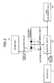
- Fig. 2 is a block diagram of a configuration of a booster according to a second embodiment useful for understanding the present invention.
- the booster circuit has a configuration that realizes an increase in the boosting capability of the booster circuit without causing an increase in minimum luminance for starting up the booster circuit.
- the configuration shown in Fig. 2 includes a selector circuit 15 in the configuration shown in Fig. 1 according to the first embodiment.
- the selector circuit 15 that two rectifier elements 32 and 33.
- the booster circuit 12 uses a power from the solar cell 14 when starting up. Moreover, after a boosting operation is started, the booster circuit 12 uses a part of the boosted power thereby drastically increasing the boosting capability of the booster. Since the power of the solar cell 14 and a part of the boosted power is selectively supplied to the booster circuit 12, the power of the solar cell 14 is supplied only to the booster circuit 12 but not to the load (secondary cell) 19, a decrease in start-up luminance can be prevented.
- the booster circuit 12 starts up when it receives a supply of power from the solar cell 14, and the booster circuit 12 supplies a power from the boosted power to the booster circuit 12 through the rectifier element 33 when boosting operation has started. As a result, the boosting capability of the booster circuit 12 increases.
- the boosting capability of the booster circuit 12 is augmented to create a virtuous cycle.
- a rectifier element that has equivalent rectifying characteristics (such as a portion between the base and emitter of a bipolar transistor) may be used instead of the rectifier elements 32 and 33. The details of the circuit configuration of the booster circuit are explained below using examples.
- the solar cell 11, which is the first cell is a single-cell solar cell that is of a low power outputting type and can be produced without complicated production processes such as configurating a serial connection.
- a single-cell fuel cell that also is of a low power outputting type and can be configured without serial connection may be used.
- parallelly connected fuel cells or solar cells that can be realized without passing complicated production processes may be used.
- the solar cell 14, which is the second cell, which plays a role of an energy source that provides start-up energy (operation energy), may be any solar cell that can supply energy.
- a lithium storage cell may be used.
- the solar cell 14 may be a primary cell, which cannot be charged, such as a dry cell, or a storage element such as an ordinary capacitor or an electric double layer capacitor.
- Fig. 3 is a diagram of a configuration of a booster circuit of a solar cell having a configuration of a boost converter according to the first example useful for understanding the present invention.
- a target to be boosted by a booster circuit 202 is a solar cell 201 that is not serially connected.
- the booster circuit 202 has an output terminal 217, to which an electronic load (Fujitsu Denso, EUL ⁇ XL150) that can be controlled to a constant current and constant voltage is connected as a load 203.
- the solar cell 201 used is a 36-square-centimeter (cm 2 ) silicon polycrystal that generates an open end output voltage at AM1.5 of 0.56 V.
- the booster circuit 202 used includes a coil 206 that has a direct current resistance of 20 milliohms, a rated current of 2 amperes (A), and an inductance value of 22 microhenries.
- a switching element 208 used includes Si9948DY manufactured by Siliconix as a MOSFET.
- a diode 207 used is a Schottky barrier diode CMS06 manufactured by Toshiba Corporation.
- a capacitor 209 used is an electrolytic capacitor manufactured by Sanyo having an electron spin resonance (ESR) of 20 milliohms and a capacitance of 220 microfarads.
- An oscillator circuit 224 includes a multivibrator oscillator circuit by means of a Schmitt trigger type inverter 74HC14, which is a versatile CMOS logic gate and a driver circuit for augmenting an output current.
- the multivibrator circuit includes a capacitor 210 that determines oscillation time constant, a resistor 211, and a Schmitt trigger type inverter 213.
- a general low power consuming type rectangular wave oscillator circuit can be used.
- the driver circuit used includes Schmitt trigger type inverters 212 and 214 connected in parallel.
- a general low power consuming type inverter or a buffer type logic gate can also be used.
- the number of parallel gates may be determined depending on the current driving capability and load. Since a supply of power to a power source terminal 215 of the Schmitt trigger type inverter 74HC14 in the oscillator circuit 224 is necessary as a power source of the booster circuit 202, the serially connected solar cell 204 and a capacitor 216 are connected to the power source terminal 15.
- As the solar cell 204 an amorphous solar cell of a 5-cell configuration manufactured by Sanyo, having a rated output of 3.0 V and 2.2 mA, and a model number of AM1156 is used.
- the capacitor 216 used is an OS electrolytic capacitor of 220 microfarads manufactured by Sanyo.
- the solar cell 201 and the solar cell 204 are arranged close to each other on a plane.
- Measurement of luminance is performed using an illuminometer 510-02 manufactured by Yokogawa Electric Corporation in such a manner that a distance from a light source and a surface of a solar cell is made equivalent to a distance from the light source and a light-receiving bulb of the illuminometer.
- the solar cell 204 provides an output voltage of about 1.9 V but does not reach rated voltage of 3.0 V. Therefore, augmentation of the supply of energy to the booster circuit after the start-up of the booster circuit was performed.
- the 74HC14 is a standard package that includes six inverter logics and power source supply terminals to the logics all together.
- the oscillator circuit 224 is configured by using the three inverter logics 21, 213, and 214 of 74HC14 and the resistor 211 and the capacitor 210.
- Fig. 4 is a diagram of a configuration of a booster circuit of a solar cell having a configuration of a boost converter according to the second example useful for understanding the present invention.
- the output from the solar cell 204 and the boosted output from the booster circuit are applied to the power source terminal 215 of the Schmitt trigger type inverter 74HC14 through an OR circuit formed by a Schottky diode 218 and a Schottky diode 219.
- the output of the solar cell 204 is supplied to the booster circuit 202 only but not to the load 203 because of the diode 219, so that the start-up illuminance is not deteriorated as compared with that of the first example.
- the voltage of the power source terminal 215 of 74HC14 increases to stabilize the operation of the oscillator circuit 224 and start driving the switching element 208 and a switching element 221 with sufficient driving capability, so that ON resistances of the switching elements 208 and 221 can be decreased.
- Si9948DY was used for the switching elements 208 and 221
- a combined value of ON-resistances obtained was 10 milliohms.
- the direct current resistance of the booster circuit reaches about 30 milliohms, so that a generated current of at most 10 A can be introduced from the solar cell 201 into the booster circuit 202 when the solar cell 201 provides a power generation voltage of 0.3 V.
- the booster circuit of this example once the booster circuit 202 is started, a part of the boosted output is supplied to the booster circuit 202, so that the solar cell 204 used for the start-up is no longer necessary.
- Table 1 shows one example of results obtained when an output voltage Vin of the solar cell 201 not serially connected, target to be boosted, was varied at various luminances.
- Table 1 Vin (V) lin (mA) Win (mW) Vout (V) lout (mA) Wout (mW) Efficiency (%) 0.50 330 165 5.002 27 135 81.9 0.40 280 112 5.002 19.1 95.5 85.0 0.30 210 63 5.002 9.7 48.5 77.0 0.20 150 30 5.002 4.7 23.5 78.4 0.10 110 11 5.002 1.9 9.5 86.4
- the electric load used as the load 203 was set at 5.00 V for a constant voltage operation.
- a boosted output was calculated from an output voltage and an output current at the output terminal 217 of the booster circuit that were measured.
- the rectangular wave oscillator circuit including a multivibrator used in the experiments was not configured so as to vary the duty ratio, so that for example, when the output voltage Vin of the solar cell 201 was 0.5 V, the supply current lin from the solar cell 201 was 330 milliamperes (mA). However, the duty ratio can be controlled.
- the 74HC14 is a standard package that includes six inverter logics and power source supply terminals to the logics all together.
- the oscillator circuit includes the three inverter logics 212, 213, and 214, the resistor 211, and the capacitor 210.
- Fig. 5 is a block diagram of a configuration of a booster according to a third embodiment useful for understanding the present invention.
- the configuration of a booster for an output from a solar cell with an output controller circuit corresponds to the configuration of the booster shown in Fig. 2 according to the second embodiment which includes an output controller circuit 16.
- the electric power generated by the solar cell 11, a target to be boosted, is boosted by the booster circuit 12 and subjected to output control for a constant voltage or constant current or for charging, and then supplied to an electric or electronic circuit or the load (secondary cell) 19, which is a secondary cell through a rectifier element 34.
- a part of the boosted power is supplied to the output controller circuit 16 and the booster circuit 12.
- the power of the solar cell 14 for starting up the booster circuit 12 is supplied to the booster circuit only by the action of the rectifier element 33, so that a decrease in the start-up luminance can be prevented.
- the output controller circuit 16 to be used may be either a 3-terminal series regulator or a simple configuration in which a constant voltage diode is used. The details of the circuit configuration of the booster circuit are explained in examples hereinbelow.
- the solar cell 11, which is the first cell is a single-cell solar cell that is of a low power outputting type and can be produced without complicated production processes such as configurating a serial connection.
- a single-cell fuel cell that also is of a low power outputting type and can be configured without serial connection may be used.
- parallelly connected fuel cells or solar cells that can be realized without passing complicated production processes may be used.
- the solar cell 14, which is the second cell, which plays a role of an energy source that provides start-up energy (operation energy), may be any solar cell that can supply energy.
- a lithium storage cell may be used.
- the solar cell 14 may be a primary cell, which cannot be charged, such as a dry cell, or a storage element such as an ordinary capacitor or an electric double layer capacitor.
- Fig. 6 is a block diagram of a configuration of a booster according to a fourth embodiment useful for understanding the present invention.
- the booster has a configuration of a booster for an output from a solar cell, aimed at making the boosting capability of the booster variable.
- Fig. 6 is intended to explain the configuration of the booster circuit shown in Fig. 5 according to the third embodiment in which a control signal is sent from the output controller circuit 16 to the booster circuit 12 to make the boosting capability of the booster variable, thereby achieving control of the target.
- the booster for an output of a solar cell shown in Fig. 6 starts up when receiving a power from the solar cell 14 at the time of start-up of the booster circuit 12. Since in this point in time, neither a boosted output is generated nor the boosted output reaches a minimum operation voltage of the controller circuit 16, there exists no control signal from the output controller circuit 16 or the output controller circuit 16 operates unstably. For this reason, the booster circuit that has started up in an undesirable signal state stops, so that there is a fear that normal operation will not be performed. To solve this problem, it is necessary that a circuit configuration having the following characteristics be adopted.
- a current driving element such as a bipolar transistor be used in a control signal outputting stage.
- the current driving element needs current for turning the element ON, and when starting up the booster circuit, the output controller circuit does not have sufficient capability for driving the current driving element.
- Setting the output terminal at a high impedance allows current to flow from the booster circuit 12 to the output controller circuit 16, so that deterioration of the start-up characteristics of the booster circuit can be prevented. Therefore, it is effective that a configuration of an open drain or an open collector by using parallelly connected resistors between the gate and source to form a current driving type be used in the control signal output stage of the output controller circuit 16.
- the details of the circuit configuration of the booster are explained in the examples hereinbelow.
- the solar cell 11, which is the first cell, is a single-cell solar cell that is of a low power outputting type and can be produced without complicated production processes such as configurating a serial connection.
- a single-cell fuel cell that also is of a low power outputting type and can be configured without serial connection may be used.
- parallelly connected fuel cells or solar cells that can be realized without passing complicated production processes may be used.
- the solar cell 14, which is the second cell, which plays a role of an energy source that provides start-up energy (operation energy), may be any solar cell that can supply energy.
- a lithium storage cell may be used.
- the solar cell 14 may be a primary cell, which cannot be charged, such as a dry cell, or a storage element such as an ordinary capacitor or an electric double layer capacitor.
- Fig. 7 is a diagram of a configuration of a booster circuit for an output of a solar cell according to the third example useful for understanding the present invention.
- a rectangular wave oscillator circuit in a booster circuit 244 includes a multivibrator oscillator circuit by means of a Schmitt trigger type two-input inverter NAND (74HC132), which is a versatile CMOS logic gate, and a driver circuit for augmenting an output current.
- the multivibrator circuit includes a capacitor 233 that determines an oscillation time constant, a resistor 232, and a Schmitt trigger type two-input NAND gate 234.
- a low power consumption type rectangular wave oscillator circuit that can be controlled of an oscillation state from outside the oscillator circuit may be used.
- the driver circuit used includes Schmitt trigger type two-input NANDs 235 and 236, and 237 connected in parallel.
- a logic gate of a general low power consuming type inverter having an excellent capability of driving current can be advantageously used.
- the number of parallel gates may be determined depending on the load. Since a supply of power to a power source terminal 230 of the Schmitt trigger type two-input NAND 74HC132 in the oscillator circuit 224 is necessary as a power source of the booster circuit 244, the serially connected solar cell 204 is connected to the power source terminal 230 through the diode 218.
- the solar cell 204 an amorphous solar cell of a 5-cell configuration manufactured by Sanyo, having a rated output of 3.0 V and 2.2 mA, and a model number of AM1156 is used.
- the capacitor 216 used is a low ESR type electrolytic capacitor of 220 microfarads manufactured by Sanyo.
- the output of power generation of the solar cell 204 and the boosted output from the booster circuit 244 are connected to the power source terminal 230 in a configuration of OR by means of the diodes 218 and 219.
- the output of power generation by the solar cell 204 can be supplied to the power source terminal 230 only and a part of the boosted output can be supplied to the power source terminal 230 without flowing back from the boosted output to the solar cell 204.
- insertion of the current limiting resistor 220 can prevent a supply of excessive power to the power source terminal 230, thereby increasing the conversion efficiency of the booster circuit.
- the diodes 218, 219, 207, and 238 are advantageously Schottky barrier diodes that have characteristics of low potential drops in the forward direction.
- CMS06 manufactured by Toshiba Corporation is used.
- the third example is an example of a circuit configuration for making a boosted output at a constant voltage when an output from a non-serially connected solar cell is boosted by the booster circuit 244. It is not essential for this booster circuit whether the boosted output is controlled to a constant voltage or a constant current and any known output-controlling technologies can be used. What is needed is where to obtain a power that is required by the output controller circuit and how to interface control signals.
- the output voltage of the solar cell 201 as a target to be boosted is about 0.4 V, at most a little higher than 0.5 V. It is impossible to drive a comparator or a standard voltage source that constitute a general output controller circuit at such a low voltage.
- the solar cell 204 another energy source, is to provide energy necessary for the start-up operation of the booster circuit 244 and it is assumed that a small area solar cell is utilized.
- the output controller circuit needs to function only when the booster circuit 244 generates a boosted output. Therefore, known output-controlling units can be used without deteriorating the characteristics of low luminance operation of the booster circuit of the present invention by connecting the output controller circuit in such a manner that a voltage is obtained from the boosted output of the non-serially connected solar cell 201 as shown in Fig. 7 .
- Output controls such as a constant voltage control and a constant current control can be realized by affecting the boosting operation of the booster circuit 244 to control the boosting capability thereof.
- the output control unit operates by obtaining a power from the boosted output from the booster circuit 244, the output control unit cannot operate until a boosted output is obtained from the booster circuit 244.
- the oscillator circuit in the booster circuit receives an oscillation permission signal that is not 0 (zero) volt to oscillate and controls the boosting operation, the following problems arise.
- the booster circuit 244 starts oscillation and performs boosting operation when an oscillation control terminal 260 receives an oscillation permission signal that corresponds to a high level of a logic.
- the oscillation control terminal 260 is connected to the power source terminal 230 through an integrator circuit that includes a resistor 231 and a capacitor 245, as shown in Fig. 7 .
- the output terminal of control signals is designed to be of an open drain configuration or an open collector configuration. In this circuit configuration, the voltage of the oscillation control terminal 260 at the time of start-up is substantially equal to the power source voltage of the power source terminal 230, so that the booster circuit has characteristics that logic high can be stably obtained.
- the constant voltage controller circuit includes a comparator 241 of an open drain output configuration, a standard voltage source 242, a bias resistor 239, and output voltage resistors 240 and 243 for setting an output voltage value, and the components are connected to each other as shown in Fig. 7 .
- the comparator 241 which may be of an open drain output configuration or an open collector configuration, or of a configuration other than these, can be connected to the oscillation control terminal 260 at the comparator output terminal through an N-type MOSFET or NPN-type bipolar transistor.
- the booster When the booster is started up by irradiation of sunlight, no boosted output is obtained, so that the N-type MOSFET or NPN transistor in the output stage of the comparator 241 is in a state of OFF, the voltage of the oscillation control terminal 260 increases, and the multivibrator in the booster circuit starts oscillation to provide a boosted output.
- the output of the comparator draws current, so that the oscillator control terminal 260 is at a logic low, resulting in that the oscillation stops and the boosting operation stops.
- the open drain output circuit of the comparator turns OFF, the voltage of the oscillation control terminal 260 increases through an integrator circuit and the logic becomes a high level and then the booster circuit 244 starts again oscillation to perform boosting operation to control the output voltage to a constant level.
- the solar cell 201 and the solar cell 204 were arranged close to each other on a plane. Measurement of luminance is performed using an illuminometer 510-02 manufactured by Yokogawa Electric Corporation in such a manner that a distance from a light source and a surface of a solar cell is made equivalent to a distance from the light source and a light-receiving bulb of the illuminometer. Results of experiments indicated that boosting operation started at 800 luxes. Adjustment of the oscillation frequency of the oscillator circuit varied a boosting start voltage and the boosting start voltage was most sensitive at an oscillation frequency of about 1 kHz to about 30 kHz.
- Fig. 8 is a diagram of a configuration of a booster circuit for an output of a solar cell that has a configuration of a boost converter with an output control function and is not serially connected according to the fourth example useful for understanding the present invention.
- the boosting capability of the booster circuit 244 is controlled through the oscillation control terminal 260 of the booster circuit 244 with the control output of the output controller circuit to realize a constant voltage output operation.
- a difference between this example and the third example is that when the oscillation control terminal 260 of the booster circuit 244 is at a logic low, the oscillator circuit operates to operate the booster circuit, thus making unnecessary a bias circuit from the power source terminal 230 that is necessary in the third example. Since the operation of the oscillator circuit stops when the oscillation control terminal 260 is at a logic high, a PNP transistor 272 or a P-type MOSFET level shifter circuit is arranged downstream of the output of the comparator. Resistors 273 and 274 are bias resistors of the PNP transistor 272.
- a resistor 270 is a pull-down resistor of the oscillation control terminal 260 and a resistor 271 is to prevent excess current from the PNP transistor 272 and to prevent latch up by application of an excess voltage to the oscillation control terminal.
- a capacitor 275 is to increase the anti-noise characteristics of the oscillator circuit control terminal.
- the voltage of the power source terminal 230 increases and the Schmitt trigger type two-input NAND logic gate 74HC132 comes to be in an active state. Since there is no boosted output, the oscillation control terminal 260 is at a logic low due to the pull-down resistor 270, so that the oscillator circuit starts oscillation and the booster circuit starts up to generate a boosted output. A voltage obtained by dividing the boosted output voltage by the divided resistors 240 and 243 and the voltage of the standard voltage source 242 are compared by the comparator 241.
- the comparator 241 connects the positive and negative input terminals of the PNP transistor 272 in a subsequent stage to each other in such a manner that when the boosted output voltage is higher than the voltage of the standard voltage source 242, the PNP transistor 272 turns ON.
- the transistor turns ON, current flows from the boosted output to the pull-down resistor 270, which brings the oscillation control terminal at a logic high, resulting in that the oscillation operation stops and the boosting operation stops.
- the output of the comparator turns OFF and the PNP transistor 272 turns OFF, so that the oscillation control terminal 260 is at a logic low.
- the oscillator circuit operates and the boosting operation starts again, so that the output voltage is controlled to a constant voltage.
- the booster of the present invention even when the output voltage is 0.15 V or less, no problems occur and a boosted voltage can be obtained at a high efficiency. Therefore, there is no need for connecting a number of single cells in series, so that the problem encountered in the conventional serially connected solar cells that when some tens percents of single-cell solar cells that constitute a solar cell module is under a shade, the same effect as that obtained when some tens percents of the entire module is under a shade is obtained, resulting a considerable decrease in output, can be solved.
- the shape of a cell is tetrangular and it has been difficult to apply a design.
- solar cells having various shapes can be used in a parallel connection so that the solar cell modules are free of restrictions on their shape since the solar cells as a power generation target do not have to be serially connected.
- Fig. 9 is a block diagram of a configuration of a booster according to a fifth embodiment useful for understanding the present invention.
- the booster includes the booster circuit 12 that boosts a low voltage output from a single-cell fuel cell 21 (i.e., the first cell) outputting a low voltage of about 0.6 V to about 0.7 V (without loads) as a target to be boosted to a predetermined voltage (for example, a voltage at which the load can operate) and a lithium storage cell 23 (i.e., the second cell) that serves as a power supply unit for providing start-up energy to the booster circuit 12.
- the fuel cell 21 merely supplies a low voltage output, a target to be boosted, to the booster circuit 12, and is not an essential constituent element of the booster of the present invention.
- the fuel cell 21 is a single-cell fuel cell of a low voltage outputting type that can be produced without passing complicated production processes such as configuring serial connection.
- the lithium storage cell 23 is a rechargeable secondary cell and plays a role of an energy source that provides start-up energy.
- the booster circuit 12 is configured by a circuit of, for example, a boost converter type, which is easy to design a circuit configuration. By performing ON/OFF control of the switching elements provided in the booster circuit, boosting of a voltage that is stored in a storage element such as a capacitor can be performed. It is preferable to use a CMOS type circuit as an oscillator circuit for performing ON/OFF control of the switching elements.
- a chemical reaction is performed between a fuel and oxygen (air) sent in the fuel cell 21 and the chemical reaction generates electric energy.
- the generated output is generally at a low voltage, for example, an output voltage of 0.6 V to 0.7 V without loads (i.e., when no load is connected) and at most about 0.3 V when a rated output is generated. Therefore, the output from the fuel cell 21 cannot directly drive mobile devices such as note-type personal computers and mobile phones.
- the low voltage output from the fuel cell 21 is input into the booster circuit 12.
- boosted electric energy is stored in a storage element such as a capacitor (not shown).
- a predetermined level of start-up energy is required.
- the lithium storage cell 23 supplies start-up energy to the booster circuit 12.
- the booster circuit 12 requires some amounts of energy at the time of start-up but the booster circuit 12 can continue the operation with a lower amount of energy than the energy given at the time of start-up once the booster circuit 12 has started up.
- the boost converter type booster circuit requires an input voltage of about 1.4 V at the time of start-up.
- the operation of the booster circuit 12 itself can be continued even with a low input voltage of about 0.1 V. Therefore, in the booster according to this embodiment, start-up energy is output from the lithium storage cell 23 to the booster circuit 12 only at the time of the start-up. After the start-up, the output of the booster circuit 12 itself is fed back to the booster circuit 12 as operation energy, so that the operation of the booster circuit 12 itself can be continued to obtain a predetermined boosted output.
- the output of the booster circuit 12, i.e., boosted output, can be set to any predetermined voltage depending on the operation voltage of the mobile device to which the booster circuit 12 is connected, so that a boosted output for operating mobile devices can be obtained by utilizing the energy of the fuel cell 21 from which only a low voltage output can be obtained.
- a low voltage output, target to be boosted, from the first cell and start-up energy from the second cell are input to the booster circuit while operation energy necessary for continuing the operation of the booster circuit itself is fed back to the booster circuit by the booster circuit itself, so that a predetermined boosted output can be obtained.
- a boosted output for operating, for example, a mobile device can be obtained by utilizing the energy of the first cell from which only a low voltage output is available and an increase in production cost because of using a special cell can be prevented, so that a booster that enables one to reduce cost by utilization of a versatile cell can be provided.
- the fuel cell 21, which is the first cell is a single-cell fuel cell of a low voltage outputting type that can be produced without passing complicated production processes such as configurating serial connection.
- a single-cell solar cell that also is of a low power outputting type and can be configured without serial connections may be used.
- parallelly connected fuel cells or solar cells that can be realized without passing complicated production processes may be used.
- the lithium storage cell 23, which is the second cell, which is a rechargeable secondary cell and plays a role of an energy source that provides start-up energy, may be any cell that can supply energy.
- the lithium storage cell may be a primary cell that is not rechargeable, such as a dry cell.
- the second cell may be a storage element such as an ordinary capacitor or an electric double layer capacitor.
- CMOS type oscillator circuit As an oscillator circuit for performing ON/OFF control of the switching elements in the booster circuit, other circuits, for example, a bipolar type oscillator circuit may be used.
- the bipolar type oscillator circuit has a disadvantage that the circuit consumes much power but has an advantage that the minimum operation voltage is low. It is also possible to design a circuit configuration making the best of this advantage.
- Fig. 10 is a block diagram of a configuration of a booster according to a sixth embodiment useful for understanding the present invention.
- the booster includes, in addition to the configuration according to the fifth embodiment as shown in Fig. 9 , a rectifier element 35 for outputting a part of the output of the booster circuit 12 to the lithium storage cell 23 as energy to be utilized for next and subsequent start-ups.
- Other configurations are the same as or equivalent to those shown in Fig. 9 and the same reference numerals designate those portions.
- the booster circuit 12 performs boosting operation using the low voltage output from the single-cell fuel cell 21, the start-up energy from the lithium storage cell 23, and operation energy that is a part of the own output and fed back to the booster circuit is the same as that in the fifth embodiment and explanation is omitted.
- all or a part of the boosted output from the booster circuit 12 is output to the lithium storage cell 23 through the rectifier element 35.
- the energy output then is energy for starting the operation of the booster circuit 12 again and is stored in the lithium storage cell 23.
- all or a part of the output of the booster circuit 12 is stored in the lithium storage cell 23 and this energy is output to the booster circuit 12 when the booster circuit 12 is restarted.
- the rectifier element 35 is provided to prevent flow of current from the lithium storage cell 23 to the side of the output (booster circuit 12) when the stored voltage of the lithium storage cell 23 is higher than the boosted output.
- a low voltage output, target to be boosted, from the first cell and start-up energy from the second cell are input to the booster circuit while operation energy necessary for continuing the operation of the booster circuit itself is fed back to the booster circuit by the booster circuit itself, so that a predetermined boosting output can be obtained.
- a boosting output for operating, for example, a mobile device can be obtained by utilizing the energy of the first cell from which only a low voltage output is available and an increase in production cost because of using a special cell can be prevented, so that a booster that enables one to reduce costs by utilization of a versatile cell can be provided.
- the booster circuit outputs a boosted output to the second cell to store therein as start-up energy for restarting the own operation of the booster circuit, so that unnecessary consumption of electric power can be prevented. Since restart is possible with the energy stored in the second cell even when the boosted output decreases due to overload, thus falling in a situation where the own boosting operation of the booster circuit cannot be continued, a configuration with which continued operation is easy can be realized with ease.
- the lithium storage cell 23 may be a primary cell that is not rechargeable, such as a dry cell in the fifth embodiment, it is necessary in the sixth embodiment to store energy for restarting the booster circuit. Therefore, it is advantageous to use a storage element such as an ordinary capacitor or an electric double layer capacitor in addition to the rechargeable secondary cell.
- Fig. 11 is a block diagram of a configuration of a booster according to a seventh embodiment useful for understanding the present invention.
- the booster includes, in addition to the configuration according to the sixth embodiment as shown in Fig. 10 , a selector circuit 25 that has rectifier elements 36 and 37 and selects which one of the start-up energy and operation energy is to be output to the booster circuit 12.
- Other configurations are the same as or equivalent to those shown in Fig. 9 and the same reference numerals designate those portions.
- the booster circuit 12 is configured in such a manner that either one of the start-up energy and operation energy is input to the booster circuit 12 through the selector circuit 25. The reason for this is as follows.
- the booster circuit 12 can continue its operation with a small amount of input voltage. That is, as in the configuration according to the seventh embodiment, inputting an output that is superior between outputs of the start-up energy and operation energy to the booster circuit 12 through the selector circuit 25 can lead to realization of efficient utilization of energy.
- the rectifier element 35 is provided so as to prevent flow of the current from the lithium storage cell 23 to the output side when the stored voltage of the lithium storage cell 23 is higher than the boosted voltage.
- the rectifier elements 36 and 37 are provided in the selector circuit 25 as units that supply a superior output (output having higher output voltage) between outputs of the start-up energy and operation energy to the booster circuit 12.
- a low voltage output, target to be boosted is input to the booster circuit 12 from the first cell and the selector circuit, to which both the start-up energy and operation energy are input, outputs either one of the start-up energy and operation energy to the booster circuit, so that not only the boosted output for operating, for example, a mobile device can be obtained by using the energy of the first cell from which only a low voltage output is available but also a booster with which an increase in production cost due to use of a special cell is prevented and reduction of cost by using a versatile cell is possible can be provided. Further, efficient utilization of boosted output energy can be realized and a system configuration having a high capacity utilization can be realized with ease.
- the first cell which is the fuel cell 21
- the first cell which is the fuel cell 21
- the first cell may be a single-cell fuel cell or a single-cell solar cell.
- parallelly connected fuel cells or solar cells may be used.
- the second cell which is the lithium storage cell 23, may be any cell that can store energy for the restart similarly to the sixth embodiment.
- a storage element such as an ordinary capacitor or an electric double layer capacitor may be used as the secondary cell.
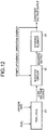
- Fig. 12 is a block diagram of a configuration of a booster according to an eighth embodiment useful for understanding the present invention.
- the booster depicted includes, in the configuration according to the fifth embodiment as shown in Fig. 9 , a storage element 24 for storing the output of the booster circuit 12 while the booster includes no lithium storage cell 23.
- Other configurations are the same as or equivalent to those shown in Fig. 9 and the same reference numerals designate those portions.
- a low voltage output is input to the booster circuit 12 from the single-cell fuel cell 21.
- the booster circuit 12 according to the eighth embodiment is configured in such a manner that both the start-up energy that is supplied when starting up and the operation energy that is continuously supplied during operation are input to the booster circuit 12 from the storage element 24.
- a countermeasure that is commonly adopted is to incorporate a constant voltage unit such as the storage element 24 between the booster circuit 12 and the load (not shown) as shown in Fig. 12 .
- the storage element 24 that provides a constant voltage, the start-up energy and operation energy output to the booster circuit 12 caused to be output from the storage element 24 to thereby start up the booster circuit 12 and continue its operation after the start-up. Accordingly, a configuration close to the actual system configuration can be obtained and the booster circuit 12 can be made compact. Further, use of the storage element 24 enables one to realize a booster having a relatively large power source capacity. Further, use of the storage element 24 enables one to realize a booster having a relatively large power source capacity.
- a low voltage output, target to be boosted is input to the booster circuit 12 from the first cell and the selector circuit, to which both the start-up energy and operation energy are input, outputs the start-up energy and operation energy to the booster circuit. Accordingly, the boosted output for operating, for example, a mobile device can be obtained by using the energy of the first cell from which only a low voltage output is available. Also, a booster having a relatively large power source capacity can be realized.
- the first cell which is the fuel cell 21
- the first cell which is the fuel cell 21
- the first cell may be a single-cell fuel cell or a single-cell solar cell.
- parallelly connected fuel cells or solar cells may be used.
- the storage element 24 may be a storage element such as an ordinary capacitor or an electric double layer capacitor.
- the booster circuit 12 and the storage element 24 are configured to be separate. However, it is possible to configure the booster in such a manner that the storage element 24 is incorporated in the booster circuit 12.
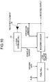
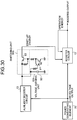
- Fig. 13 is a block diagram of a configuration of a booster according to a ninth embodiment useful for understanding the present invention.
- the booster depicted is configured to include, in addition to the configuration according to the eighth embodiment as shown in Fig. 12 , a selector circuit 26 that has rectifier elements 45 and 46 and selects which one of the start-up energy and operation energy is to be output to the booster circuit 12 and a rectifier element 44 that prevents flow back from the storage element 24 to the booster circuit 12.
- Other configurations are the same as or equivalent to those shown in Fig. 12 and the same reference numerals designate those portions.
- the booster circuit 12 is configured in such a manner that only the operation energy is supplied by the booster circuit 12.
- a superior output between outputs of the start-up energy and the operation energy is supplied to the booster circuit 12 through the selector circuit 26. That is, when the booster is started up, usually the booster circuit 12 is in a state where the operation stops and hence the output voltage of the storage element 24 (start-up energy) is higher than the output voltage of the booster circuit 12 (operation energy). Accordingly, the start-up energy is supplied to the booster circuit 12 through the rectifier element 46.
- the output voltage of the booster circuit 12 (operation energy) is higher than the output voltage of the storage element 24 (start-up energy). Accordingly, the operation energy is supplied to the booster circuit 12 itself through the rectifier element 45.
- a low voltage output, target to be boosted is input to the booster circuit 12 from the first cell and the selector circuit, to which both the start-up energy that is an output from the storage element and the operation energy that is an output from the booster circuit are input, outputs either one of the start-up energy and operation energy to the booster circuit.
- the boosted output for operating for example, a mobile device can be obtained by using the energy of the first cell from which only a low voltage output is available.
- a booster with which an increase in production cost due to use of a special cell is prevented and a reduction of cost by using a versatile cell is possible can be provided.
- the load on the storage element can be reduced and efficient utilization of boosted output energy can be realized.
- the first cell which is the fuel cell 21
- the first cell which is the fuel cell 21
- the first cell may be a single-cell fuel cell or a single-cell solar cell.
- parallelly connected fuel cells or solar cells may be used.
- the storage element 24 may be a storage element such as an ordinary capacitor or an electric double layer capacitor.
- the booster circuit 12 and the storage element 24 are configured to be separate. However, it is possible to adopt a configuration in which the storage element 24 and the rectifier element 44 are incorporated in the booster circuit 12.
- Fig. 14 is a block diagram of a configuration of a booster according to a tenth embodiment useful for understanding the present invention.
- the booster depicted includes, in the configuration according to the fifth embodiment as shown in Fig. 9 , a fuel etc. supply detecting unit 29 that detects whether a fuel or oxygen (air) is supplied to the fuel cell 21, a switching unit 27 provided with a switching element 51 that is connected between the lithium storage cell 23 and the booster circuit 12 and to which a start-up signal from the fuel etc. supply detecting unit 29 and a supply stop signal from the booster circuit 12 are input.
- Other configurations are the same as or equivalent to those shown in Fig. 9 and the same reference numerals designate those portions.
- the fuel etc. supply detecting unit 29 detects that a fuel or oxygen (air) (hereinafter, referred to as "fuel etc.”) is supplied to the fuel cell 21 and outputs a start-up signal.
- the booster circuit 12 generates a boosted output formed by boosting a low voltage output from the fuel cell 21.
- the switching unit 27 controls whether to output the start-up energy supplied from the lithium storage cell 23 to the booster circuit 12 based on the start-up signal that is output from the fuel etc. supply detecting unit 29 and the supply stop signal that is output from the booster circuit 12.
- the output of the booster circuit 12 is fed back to the booster circuit 12 itself, so that the booster circuit 12 can continue its boosting operation.
- the fuel etc. supply detecting unit 29 outputs a start-up signal while the fuel etc. is supplied to the fuel cell 21.
- the start-up signal is output while the fuel etc. is supplied (start-up signal "ON"), and acts in such a manner that the switching element 51 of the switching unit is conducting.
- the supply stop signal is the boosted output itself of the booster circuit 12 and acts in such a manner that when the boosted output voltage is a predetermined voltage or more (supply stop signal "ON"), the switching element 51 of the switching unit 27 is interrupted while when the boosted output voltage is less than the predetermined voltage (supply stop signal "OFF”), the switching element 51 is conducting.
- the relationship between the start-up signal and supply stop signal and the switching unit 27 is as follows. That is, when the start-up signal is in a state of ON and the supply stop signal is in a state of OFF, the switching element 51 is conducting and the start-up energy is supplied from the lithium storage cell 23 to the booster circuit 12.
- the switching element 51 When the start-up signal is in a state of OFF, or the supply stop signal is in a state of ON, the switching element 51 is interrupted, so that there is no supply of the start-up energy to the booster circuit 12.
- the booster according to this embodiment is in as state where the fuel etc. is supplied to the fuel cell, and when the booster circuit 12 has not started up yet, the start-up energy is output to the booster circuit 12 from the lithium storage cell 23.
- efficient use of the start-up energy is made possible by controlling in such a manner that the start-up energy is output only when it is necessary to start up the booster circuit 12.
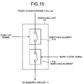
- Fig. 15 is a block diagram of the switching unit 27 shown in Fig. 14 with serially connected switching elements 51a and 51b.
- the function of the switching unit 27 shown in Fig. 14 can be easily realized by connecting the start-up signal to the switching element 51a and the supply stop signal to the switching element 51b.
- the switching unit to which a low voltage output from the first cell is input controls whether to allow the start-up energy supplied from the second cell to be output to the booster circuit based on the start-up signal output from the fuel etc. supply detecting unit and the supply stop signal that is the boosted output itself, so that the boosted output for operating, for example, a mobile device can be obtained by using the energy of the first cell from which only a low voltage output is available. Also, the start-up energy can be output only when it is necessary to start up the booster circuit, so that it is possible to use the start-up energy efficiently.
- the lithium storage cell 23, which is the second cell, which is a rechargeable secondary cell and plays a role of an energy source that provides start-up energy, may be any cell that can supply energy.
- the lithium storage cell may be a primary cell that is not rechargeable, such as a dry cell.
- the second cell may be a storage element such as an ordinary capacitor or an electric double layer capacitor.
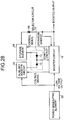
- Fig. 16 is a block diagram of a configuration of a booster according to an eleventh embodiment useful to understand the present invention.
- the booster includes, in addition to the configuration according to the tenth embodiment as shown in Fig. 14 , the selector circuit 25 that has the rectifier elements 36 and 37 and selects which one of the start-up energy and operation energy is to be output to the booster circuit 12 and the rectifier element 35 for outputting all or a part of the output of the booster circuit 12 to the lithium storage cell 23.
- Other configurations are the same as or equivalent to those shown in Fig. 14 and the same reference numerals designate those portions.
- all or a part of the boosted output from the booster circuit 12 is output to the lithium storage cell 23 through the rectifier element 35.
- the rectifier element 35 is provided so as to prevent a backflow of current from the lithium storage cell 23 to the booster circuit 12.
- the switching unit 27 controls whether to output the start-up energy supplied from the lithium storage cell 23 to the booster circuit 12 based on the start-up signal output from the fuel etc. supply detecting unit 29.
- the start-up signal is output is a start-up signal ("ON" signal) for conducting the switching unit 27 while the fuel etc. is being supplied. On this occasion, the energy from the lithium storage cell 23 is output to the selector circuit 25.
- the selector circuit 25 outputs to the booster circuit 12 a superior output between outputs of the start-up energy that is output from the switching unit 27 and the operation energy that is a boosted output from the booster circuit 12.
- the booster circuit 12 to which the start-up energy or operation energy is supplied generates and outputs a predetermined boosted output.
- a low voltage output, target to be boosted is input to the booster circuit from the first cell and the selector circuit, to which both the start-up energy and operation energy are input through the switching unit that operates based on the start-up signal output from the fuel etc. supply detecting unit, outputs either one of the start-up energy and operation energy to the booster circuit. Accordingly, not only the boosted output for operating, for example, a mobile device can be obtained by using the energy of the first cell from which only a low voltage output is available but also a booster with which an increase in production cost due to use of a special cell is prevented and a reduction of cost by using a versatile cell is possible can be provided. Also, the start-up energy can be output only when it is necessary to start up the booster circuit, so that it is possible to use the start-up energy efficiently.
- the feature of this embodiment i.e., the configuration in which the start-up energy is output based on the start-up signal output from the fuel etc. supply detecting unit and a control whether to allow either the start-up energy or the operation energy to be output to the booster circuit is performed can be applied to the eighth and ninth embodiments with similar effects as those of the eleventh embodiment.
- the lithium storage cell 23, which is the second cell, which is a rechargeable secondary cell and plays a role of an energy source that provides start-up energy, may be any cell that can supply energy.
- the lithium storage cell may be a primary cell that is not rechargeable, such as a dry cell.
- the second cell may be a storage element such as an ordinary capacitor or an electric double layer capacitor.
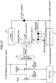
- Fig. 17 is a block diagram of a configuration of a booster according to a twelfth embodiment useful to understand the present invention.
- the booster is configured in such a manner that in the configuration according to the eleventh embodiment as shown in Fig. 17 , the start-up signal to be output to the switching unit 27 is output as follows. That is, a power generation request signal to be given to control valves 42 and 43 for controlling fuel and oxygen (air), respectively, supplied to the fuel cell 21 is output through a signal delay circuit 28 as the start-up signal.
- Other configurations are the same as or equivalent to those shown in Fig. 16 and the same reference numerals designate those portions.
- a power generation request signal is input to the control valves 42 and 43, the control valves 42 and 43 are opened and fuel and oxygen are supplied to the fuel cell 21.
- the power generation request signal is input to the signal delay circuit 28.
- the signal delay circuit 28 outputs to the switching unit 27 a signal that is delayed a predetermined time with respect to the input power generation request signal.
- a certain time is required for fuel and oxygen to distribute in the fuel cell. Therefore, by delaying a timing in which the switching unit 27 turns ON by a predetermined time behind a timing in which fuel and oxygen are sent to the fuel cell 21, the timing in which the output of the fuel cell 21 is output to the booster circuit 12 and the timing in which the start-up energy is output to the booster circuit 12 are synchronized with each other so that efficient use of the start-up energy is possible.
- a delay time that is delayed by the signal delay circuit 28 only needs to be set to a time from a time when the power generation request signal is input to when the fuel etc. is distributed in the inside of the fuel cell 21 and may be set to any time depending on the system of the fuel cell. Note that the operation thereafter is similar to that in the eleventh embodiment, and a predetermined boosted output can be obtained by the booster circuit 12 can provide.
- a low voltage output, target to be boosted is input to the booster circuit from the first cell and the selector circuit, to which both the start-up energy through the switching unit that operates based on the start-up signal output and the operation energy as an output of the booster circuit are input, outputs either one of the start-up energy and operation energy to the booster circuit.
- a mobile device can be obtained by using the energy of the first cell from which only a low voltage output is available but also a booster with which an increase in production cost due to use of a special cell is prevented and a reduction of cost by using a versatile cell is possible can be provided.
- the start-up energy can be output only when it is necessary to start up the booster circuit, so that it is possible to use the start-up energy efficiently.
- the feature of this embodiment i.e., the configuration in which the start-up energy is output based on the delayed output of the power generation request signal and a control whether to allow either the start-up energy or the operation energy to be output to the booster circuit is performed can be applied to the eighth and ninth embodiments with similar effects as those of the twelfth embodiment.
- the lithium storage cell 23, which is the second cell, which is a rechargeable secondary cell and plays a role of an energy source that provides start-up energy, may be any cell that can supply energy.
- the lithium storage cell may be a primary cell that is not rechargeable, such as a dry cell.
- the second cell may be a storage element such as an ordinary capacitor or an electric double layer capacitor.
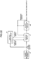
- Fig. 18 is a block diagram of a configuration of a booster according to a thirteenth embodiment useful to understand the present invention.
- the booster includes the booster circuit 12 that boosts a low voltage output from a power generating element 20 as a target to be boosted to about a predetermined voltage (for example, a voltage at which a load to be connected can operate) and an auxiliary booster circuit 13 provided to give start-up energy to the booster circuit 12.
- the power generating element 20, which supplies a low voltage output, a target to be boosted, to the booster circuit 12, is not a constituent element of the booster of the present invention.
- the power generating element 20 that can be used include, for example, a single-cell fuel cell that outputs a low voltage as low as about 0.6 V to about 0.7 V without loads, and single-cell soar cells that have a composition of a monocrystalline silicon, polycrystalline silicon, amorphous silicon, and a compound semiconductor and output a low voltage of at most a little higher than 0.5 V.
- the booster circuit 12 includes, for example, a switching regulator type circuit, with which it is easy to design a circuit configuration, and a boosted output can be obtained by generating energy of counterelectromotive force by ON/OFF control of the switching element provided in the booster circuit itself and storing the energy in a storage element such as a capacitor in the inside of the booster circuit itself.
- the auxiliary booster circuit 13 includes, for example, a switched capacitor type circuit or a charge pump type circuit.
- the feature of the auxiliary booster circuit 13 is that the auxiliary booster circuit 13 can start-up at a low voltage as low as about 0.2 V to about 0.3 V and provides an output voltage of 1.2 V to 3 V depending on the number of connection stages of the storage elements. Therefore, the booster circuit 12 can be started up based on the start-up energy supplied by the auxiliary booster circuit 13.
- the details of the switched capacitor type circuit and of the charge pump type circuit are explained.
- Electric energy is generated in the power generating element 20.
- An output based on the generated electric energy is generally at a low voltage.
- the output is about 0.6 to about 0.7 V in the absence of loads or at most around 0.3 V when rated output is produced.
- the output is at most a little higher than 0.5 V when it is fine or at most around 0.3 V when it is clouded. That is, the output from the power generating element 20 alone cannot directly allow a mobile device such as a note type personal computer or a mobile phone to operate.
- the low voltage output from the power generating element 20 is input to the booster circuit 12.
- boosted electric energy is accumulated in a storage element such as a capacitor (not shown).
- a predetermined amount of start-up energy is required for operating the booster circuit 12.
- the auxiliary booster circuit 13 supplies a start-up voltage to the booster circuit 12.
- the booster circuit 12 requires about 1 V when starting up but it is featured that a small amount of start-up current is sufficient. Therefore, in the booster according to the thirteenth embodiment, the booster circuit 12 is started up with the start-up voltage from the auxiliary booster circuit 13 when starting up, and after the start-up, the own output is fed back to the booster circuit 12 as operation energy for continuing the operation of the booster circuit 12 to obtain a boosted output.
- This configuration has an advantage that no power supply unit is necessary for starting up the booster circuit.
- the booster circuit for example, in the case of a general switching regulator type booster circuit, an input voltage of about 0.9 V to about 1.2 V is necessary when starting up while after the start-up, the operation of the booster circuit 12 itself can be continued even with a low input voltage of about 0.1 V.
- the output of the booster circuit 12, that is, a boosted output can be set at any predetermined voltage depending on the operation voltage of, for example a mobile device to be connected. Therefore, a predetermined boosted output for operating a mobile device or the like can be obtained by utilizing the energy of the power generating element 20 that can provide only a low voltage output.
- Fig. 19 is a schematic for explaining a principle of operation of a switched capacitor type.
- V dd designates a direct current voltage and corresponds to the low voltage output that is output by the power generating element 20 shown in Fig. 18 .
- SW 11 to SW 15 and SW 21 to SW 28 designate switching elements of a MOSFET or the like and controlled to either one of a state of ON and a state of OFF by, for example, a controller circuit not shown.
- Capacitors C 11 to C 15 are storage elements for storing charge.
- the capacitor C 15 is a storage element that stores start-up energy (output of the auxiliary booster circuit) for starting up the booster circuit 12.
- Fig. 19 the operation of the switched capacitor type circuit is explained.
- all of SW 21 to SW 28 are in a state of ON (closed) and all of SW 11 to SW 15 are in a state of OFF (open).
- the capacitors C 11 to C 15 are in as state where they are connected in parallel on the part of the direct current voltage V dd , so that the capacitors C 11 to C 15 are charged (charge is accumulated) to a voltage of approximately V dd .
- Fig. 20 is a schematic for explaining a circuit configuration and a principle of operation of a charge pump type.
- V dd designates a direct current voltage and corresponds to the low voltage output that is output by the power generating element 20 shown in Fig. 18 .
- Reference symbols SW 31 to SW 35 and SW 41 to SW 48 designate switching elements of a MOSFET or the like and controlled to either one of a state of ON and a state of OFF by, for example, a controller circuit not shown.
- Capacitors C 11 to C 15 are storage elements for storing charge.
- the capacitor C 15 is a storage element that stores start-up energy (output of the auxiliary booster circuit) for starting up the booster circuit 12.
- the charged pump type circuits like the switched capacitor type circuits, can be constituted by capacitors and switching elements alone.
- SW 31 , SW 33 , and SW 35 are in a state of ON and SW 32 and SW 34 are in a state of OFF.
- SW 41 , SW 44 , SW 45 , and SW 48 are in a state of ON while SW 42 , SW 43 , SW 46 , and SW 47 are in a state of OFF.
- the capacitor C 31 is charged (charge is accumulated) to approximately a voltage of V dd and a potential V1 on the upper end of the capacitor C 31 becomes approximately V dd .
- the capacitors C 32 , C 33 , and C 34 are charged to voltages of approximately 2V dd , 3V dd , and 4V dd , respectively, so that potentials V 2 , V 3 , V 4 , and V 5 of the respective upper ends of the capacitors C 32 , C 33 , and C 34 become approximately 3V dd , 4V dd , 5V dd , and 5V dd , as shown in Fig. 20 .
- the states as shown in the lower part of Fig. 20 appears.
- the charge is transferred from the power generation element (V dd ) to the first stage, between the second stage (capacitor C 32 ) and the third stage (capacitor C 33 ), and between the fourth stage (capacitor C 34 ) and the fifth stage (capacitor C 35 ).
- the charged pump type circuit shown in Fig. 20 is configured to secure a predetermined voltage and a predetermined current capacity in the same manner as that of the switched capacitor type circuit by repeating such a bucket-relay type charge transfer alternately.
- the switched capacitor type circuit and charged pump type circuit used as the auxiliary booster circuit 13 have low boosting capability and low boosting efficiency as compared with the switching regulator type circuit and the like used as the booster circuit 12. If switching regulator type circuits are named high efficiency large power type booster circuits, switched capacitor type circuits and charged pump type circuits can be named low efficiency small power type booster circuits.
- switched capacitor type circuits and charged pump type circuits can be configured by capacitors and switching elements such as MOSFETs alone.
- the switching elements such as MOSFETs can perform switching operation at a low voltage of about 0.2 V to 0.3 V.
- switching regulator type circuit requires a start-up voltage of 0.9 V or more but requires not so much of a start-up current. Therefore, use of a switched capacitor type circuit or a charged pump type circuit for starting up a switching regulator type circuit enables one to utilize both the features effectively.
- the booster circuit of a low efficiency small power type between a power generating element of which the power generation voltage is not made so high and the booster circuit of a high efficiency large power type so as to operate in such a manner that the defects of both can be compensated.
- an output of the auxiliary booster circuit which is start-up energy necessary for the start-up of the booster circuit 12 itself, is input to the booster circuit 12, or operation energy necessary for continuing the operation of the booster circuit 12 itself is fed back from the booster circuit 12 itself.
- Fig. 21 is a diagram of a configuration of a booster according to a fourteenth embodiment useful to understand the present invention.
- the booster is configured to efficiently utilize the generated energy of the power generating element.
- the configuration shown in Fig. 21 is designed in such a manner that in the configuration according to the thirteenth embodiment as shown in Fig. 18 , a control signal for judging whether to stop the start-up of the auxiliary booster circuit 13 is output from the booster circuit 12 to the auxiliary booster circuit 12.
- the booster circuit 12 performs boosting operation by using either one of the start-up energy from the auxiliary booster circuit 13 and the operation energy obtained by feeding back a part of the output of the booster circuit 12 itself is the same as the first embodiment, so that description thereof is omitted.
- the booster according to the fourteenth embodiment is configured in such a manner that after the start-up of the booster circuit 12, a control signal is output from the booster circuit 12 to the auxiliary booster circuit 13 to stop the supply of the operation energy that is output to the booster circuit 12 from the auxiliary booster circuit 13.
- a boosted output itself that is output from the booster circuit 12 can be used as the control signal.
- the judgment whether to stop the supply of the start-up energy may be performed based on the level of the boosted output. For example, control can be performed in such a manner that when the level of the boosted output exceeds a predetermined value, the supply of the operation energy stops while when the level of the boosted output is less than the predetermined value, the supply of the operation energy continues.
- Control of operation/non-operation in the inside of the auxiliary booster circuit 13 can be performed by stopping an oscillator circuit that switches the switched capacitor circuit upon receipt of a control signal therefor.
- the start-up of the auxiliary booster circuit is controlled based on the boosted output, so that after the start-up of the booster circuit, all of the generated energy of the power generating element can be directed to power generation, thereby promoting efficient utilization of generated energy.
- Fig. 22 is a diagram of a configuration of a booster according to a fifteenth embodiment useful to understand the present invention.
- the booster is of a configuration which includes an output control circuit 16a that is connected to an output stage of the booster circuit 12 in series.
- Other configurations are the same as or equivalent to those in the fourteenth embodiment and the same reference numerals as those in each circuit shown in Fig. 21 designate those portions.
- the booster circuit 12 performs boosting operation using either one of the start-up energy from the auxiliary booster circuit 13 and the operation energy obtained by feeding back a part of the output of the booster circuit 12 itself is the same as those in the first and second embodiments, so that description thereof is omitted.
- the boosted output that is boosted by the booster circuit 12 is output, for example, as a constant voltage output by an output controller circuit 16a and a stable constant voltage output is supplied to a load (not shown). Further, in the same manner as in that in the fourteenth embodiment, when a predetermined boosted output is provided, the output of the start-up energy from the auxiliary booster circuit 13 stops based on the control signal (start-up stop control signal) from the booster circuit 12.
- the output of the output controller circuit 16a is made a constant current output and a secondary cell for storing this energy may be directly connected to the output control circuit 16a.
- a rectifier element may be connected between the output controller circuit 16a and the secondary cell.
- the secondary cell may be connected between the output controller circuit 16a and the power generating element 20 may be connected between the output controller circuit 16a and the secondary cell through a rectifier element.
- Fig. 23 is a diagram of a configuration that includes a constant voltage element (Zener diode) as one example of the output controller circuit 16a.
- Fig. 24 is a diagram of a configurationthat includes a constant voltage element 61 (Zener diode) and a constant current element 62 as one example of the output controller circuit 16.
- a constant voltage output or a constant current output can be easily generated so that a booster having an output control function can be realized at low cost and in a compact form.
- a 3-terminal series regulator or the like may be used as another configuration of the output controller circuit 16. This increases the stability of the output voltage.
- the output control is performed for obtaining a constant voltage or constant current, so that in addition to the effects of the first and second embodiments, respectively, the effect of supplying a stable output to a load can be obtained.
- Fig. 25 is a diagram of a configuration of a booster according to a sixteenth embodiment useful to understand the present invention.
- the booster is of a configuration which includes an output control circuit 16b that is connected to an output stage of the booster circuit 12 in parallel.
- Other configurations are the same as or equivalent to those in the fourteenth embodiment and the same reference numerals as those in each circuit shown in Fig. 21 designate those portions.
- the operation of this booster circuit is explained.
- the feature that the booster circuit 12 performs boosting operation using either one of the start-up energy from the auxiliary booster circuit 13 and the operation energy obtained by feeding back a part of the output of the booster circuit 12 itself and the feature that when a predetermined boosted output is obtained, the output of the start-up energy from the auxiliary booster circuit 13 stops based on the control signal from the booster circuit 12 are the same as the fourteenth embodiment, so that description thereof is omitted.
- the boosted output that is boosted by the booster circuit 12 is subjected to feedback control by the output controller circuit 16b and is output as a constant voltage variable output. That is, the booster according to the sixteenth embodiment has a function to maintain the output of the booster circuit 12 at a constant voltage by the output control circuit 16b and vary the output voltage in accordance with a load capacity.
- This constant voltage varying function can be realized by a configuration in which the booster circuit 12 includes a circuit of a switching type and the output control circuit 16b performs control such as pulse width modulation (PWM) control or pulse frequency modulation (PFM) control to the booster circuit 12.
- PWM pulse width modulation
- PFM pulse frequency modulation
- Fig. 26 is a diagram of one example of a configuration of the output controller circuit 16b.
- the output control circuit 16b includes a time ratio modulator circuit 64, an oscillator circuit 65, and a comparator circuit 66.
- the output control circuit 16b operates as follows.
- the comparator 66 in the output controller circuit 16b compares the output of the booster circuit 12 and a predetermined standard voltage value 67 and a differential output voltage between these outputs is output to the time ratio modulator circuit.
- Time ratio modulator circuit 64 generates, for example, a PWM control signal to a triangular wave that is output from the oscillator circuit 65 based on the differential output voltage that is output from the comparator circuit 66 and outputs it to the booster circuit 12.
- a configured is adopted in such a manner that the boosted output of the booster circuit 12 is subjected to feedback control by the output controller circuit 16b, so that the output voltage is stabilized.
- a configuration is adopted in such a manner that the output voltage can vary based on the standard voltage value 67, so that a variable output of a constant voltage can be obtained.
- a boosted output of the booster circuit 12 is subjected to feedback control by the output controller circuit 16b and the output voltage is made variable based on the standard voltage, so that in addition to the effects of the first to third embodiments, a variable and stabilized output can be obtained in accordance with a load capacity.
- Fig. 27 is a diagram of a configuration of a booster according to a seventeenth embodiment useful to understand the present invention.
- the booster depicted in Fig. 27 is configured in such a manner that in the booster according to the fifteenth embodiment shown in Fig. 22 , a control signal is transmitted from the output control circuit 16 to the booster circuit 12 to make the boosting capability variable, thereby achieving a control objective.
- Other configurations are the same as or equivalent to those of the fifteenth embodiment and the same reference numerals as those shown in Fig. 22 designate those portions.
- the booster circuit 12 receives start-up energy from the auxiliary booster circuit 13 and starts up. In this point in time, no boosted output is generated or a boosted output does not reach the minimum operation voltage of the output controller circuit 16. Therefore, in this point in time, no control signal from the output controller circuit 16 is present or an unstable control signal is present. For this reason, there is a fear that the booster circuit 12 that has come to start up will stop due to an undesirable state of the control signal, thus failing to operate normally. To solve this problem, a circuit configuration having the following characteristics must be adopted.
- a current driving element such as a bipolar transistor in a control signal outputting stage.
- a predetermined current is necessary for turning the element ON, so that wrong operation of the element can be prevented at the time of starting up the booster circuit 12 or after the start-up thereof.
- Making the output terminal at a high impedance results in a flow of current from the booster circuit 12 to the control output terminal of the output control circuit 16a, so that deterioration of the start-up characteristics of the booster circuit can be prevented. Therefore, it is effective to adopt open drain configuration that is made a current-driven type by connecting a resistor in parallel to the open collector or to between the gate and source in a control signal output stage of the output controller circuit 16a.
- the booster circuit controls boosting capability based on the control output of the output controller circuit. Accordingly, the output controller circuit is prevented from performing an undesirable control to the booster circuit that has just come to start up and is in an unstable state, such as a state immediately after the start-up.
- Fig. 28 is a diagram of a configuration of a booster according to an eighteenth embodiment useful to understand the present invention.
- the booster includes, in the configuration according to the thirteenth embodiment shown in Fig. 18 , a storage element 58 that stores a part of the output of the booster circuit 12 as energy to be used upon a next or subsequent start-up, a rectifier element 68 for preventing flow back that prevents flow of the output of the storage element 58 to the load side, and a selector circuit 70 including rectifier elements 72 and 73 for selecting either one of the auxiliary booster circuit 13 and the storage element 58 as a source that provides start-up energy.
- Other configurations are the same as or equivalent to those of the fifteenth embodiment and the same reference numerals as those shown in Fig. 18 designate those portions.
- the booster circuit 12 performs boosting operation using the operation energy that is a part of its own output fed back to the booster circuit itself after the start-up is the same as that in the other embodiments and explanation will be omitted herein.
- the booster circuit 12 receives either one of the start-up energy form the auxiliary booster circuit 13 and the start-up energy from the storage element 58 and starts up.
- the selector circuit 70 provided with the rectifiers 72 and 73, one of the output voltage of the auxiliary booster circuit 13 and the output voltage of the storage element 58, which is higher, is selected and output to the booster circuit 12.
- the booster circuit 12 supplies a predetermined boosted output to, for example, a load (not shown). A part of the boosted output is stored in the storage element 58 through the rectifier element 24 as energy for restarting the booster circuit 12.
- the operation of the booster circuit 12 becomes unstable, so that it becomes necessary to stop the booster circuit 12.
- new start energy is required.
- the output of the booster circuit 12 is stored in the storage element 58 as energy for restarting the booster circuit 12 itself, not only the start-up energy from the auxiliary booster circuit 13 but also the start-up energy from the storage element 58 can be used when the booster circuit 12 is restarted.
- the booster circuit can be restarted using the start-up energy from the storage element 58, not only the restart time of the booster circuit 12 can be shortened as compared with the case where the auxiliary booster circuit 13 is used but also the booster circuit 12 can be started up reliably. If the predetermined boosted output is output from the booster circuit 12, similarly to the fourteenth embodiment, it is only necessary to stop outputting of the start-up energy from the auxiliary booster circuit 13 and storage element 58 based on the control signal from the booster circuit 12.
- the booster With the booster according to the eighteenth embodiment, all or a part of the boosted output is stored in the storage element (power storing unit) as energy for restarting the own operation and either one of the first start-up energy that is start-up energy output from the auxiliary booster circuit and the second start-up energy that is start-up energy output from the storage element is output to the booster circuit. Accordingly, the start-up of the booster circuit can be performed reliably.
- the storage element is used as an element for storing start-up energy for restarting
- a secondary cell or the like may also be used. Use of the secondary cell enables one to perform the start-up of the booster circuit more reliably.
- Fig. 29 is a diagram of a configuration of a booster according to a nineteenth embodiment of the present invention.
- the booster has a configuration that additionally includes a voltage judging part 82a that controls timing in which the auxiliary booster circuit outputs based on an output value (voltage) of an output of the auxiliary booster circuit output to the booster circuit 12 and a switching part 83a.
- Other configurations are the same as or equivalent to those of the thirteenth embodiment and the same reference numerals designate those portions.
- the booster circuit 12 performs boosting operation using either the start-up energy that is an output (auxiliary booster circuit output) of the auxiliary booster circuit 13 or the operation energy that is a part of its own output fed back to the booster circuit itself is the same as that in the other embodiments and explanation is omitted.
- the output from the auxiliary booster circuit 13 (i.e., output from the auxiliary booster circuit) is stored in a capacitor 86 in the voltage judging part 82a, and the stored voltage is compared in the comparator circuit 84 with a standard voltage value (V 0 ) generated by a constant voltage element 85, such as a Zener diode.
- V 0 a standard voltage value generated by a constant voltage element 85, such as a Zener diode.
- a switching element provided in the switching part 83a such as a MOSFET 87, becomes conducting to output the output of the auxiliary booster circuit (start-up energy) to the booster circuit 12.
- the switching element in the switching part 83a When the stored voltage of the capacitor 86 is not above the standard voltage value (V 0 ), the switching element in the switching part 83a is not conducting, so that the supply of the auxiliary booster circuit output to the booster circuit 12 is suspended.
- the standard voltage (V 0 ) determined by the capacitor 86 and the constant voltage element 85 may be advantageously adjusted to an optimum value, for example, in such a manner that when the energy stored in the capacitor in the last stage of the switched capacitor type circuit shown in Fig. 19 or the charged pump type circuit shown in Fig. 20 reaches a predetermined energy level that is sufficient for starting up the booster circuit 12, the switching element, such as the MOSFET 87, turns on.
- the output current that is output from the auxiliary booster circuit 13 is lower than the current necessary for starting up the booster circuit 12.
- the current for starting up the booster circuit 12 (start-up current) is insufficient. Accordingly, there is a possibility that the output voltage of the auxiliary booster circuit immediately after the booster circuit 12 is started up instantaneously lowered, resulting in a failure to start up the booster circuit 12.
- the power generating element 20 is a solar cell
- a boosted output can be obtained at a lower luminance.
- luminance gradually increases from dawn, so that the booster starts up automatically, and a boosted output can be obtained for a long time.
- the voltage judging includes a comparator that compares the auxiliary booster circuit output with a predetermined standard voltage and the switching element provided in the switching part is controlled based on the result of comparison by the comparator. Accordingly, the start-up of the booster circuit can be performed reliably independently of the power generation state of the power generating element.
- the booster according to this embodiment includes, in the booster according to the thirteenth embodiment shown in Fig. 18 , the voltage judging part 82a and the switching part 83a between the auxiliary booster circuit and the booster circuit, a configuration equivalent to this may be applied to the boosters according to the fourteenth and the fifteenth embodiments with similar effects as those of the booster according to the nineteenth embodiment.
- Fig. 30 is a diagram of a configuration of a booster according to a twentieth embodiment of the present invention.
- the booster depicted in Fig. 30 is configured in such a manner that instead of the voltage judging part 82a and the switching part 83a, a voltage judging part 82b and a switching part 83b that have similar functions as those of the voltage judging part 82a and the switching part 83a, respectively, are provided.
- Other configurations are the same as or equivalent to those of the nineteenth embodiment and the same reference numerals designate those portions.
- the voltage judging part 82b includes a resistor, a capacitor 50, Darlington-connected transistors 91 and 92, and so on and when a stored voltage that is stored in the capacitor in the last stage in the auxiliary booster circuit 13 exceeds V BE (that is approximately equal to 1.2 V) of the Darlington-connected transistors 91 and 92, a switching element 93 in the switching part 83b becomes conducting, so that start-up energy is supplied to the booster circuit 12.
- V BE that is approximately equal to 1.2 V
- the voltage judging part 82b includes the Darlington-connected transistors 91 and 92
- the present invention is not limited to this connection and a configuration in which a resistor, a rectifier element and so on are combined and a voltage drop that occurs in the rectifier element is utilized may also be used.
- the booster according to the twentieth embodiment provides effects equivalent to those of the booster according to the nineteenth embodiment but requires no comparator in contrast to the voltage judging part 82a in the nineteenth embodiment. This provides advantages that power consumption reduces to improve the efficiency of energy storage in the storage element and cost decreases.
- the voltage judging part includes Darlington-connected transistors that become conducting when the auxiliary booster circuit output reaches a predetermined voltage and the switching element provided in the switching part is controlled based on the auxiliary booster circuit output and the voltage drop that occurs between the base and emitter of the Darlington-connected transistors. Accordingly, the start-up of the booster can be performed reliably independently of the power generation state of the power generating element.
- the booster according to the embodiment is configured to include the voltage judging part 82b and the switching part 83b between the auxiliary booster circuit and the booster circuit, a configuration equivalent to this may also be applied to the boosters according to the fourteenth to seventeenth embodiments with similar effects to those of the twentieth embodiment.
- the booster according to the present invention is useful as a booster for use in a power source for mobile devices, and in particular, the booster according to the present invention is suitable when an output of a fuel cell or an output of a solar cell is used as an energy source.
Landscapes
- Engineering & Computer Science (AREA)
- Power Engineering (AREA)
- Dc-Dc Converters (AREA)
- Control Of Electrical Variables (AREA)
- Photovoltaic Devices (AREA)
Claims (3)
- Survolteur comprenant :un circuit de survolteur (12) prévu pour recevoir l'une ou l'autre d'une énergie de démarrage nécessaire pour démarrer le circuit de survolteur (12) et d'une énergie de fonctionnement nécessaire pour poursuivre un fonctionnement du circuit de survolteur (12), dans lequel le circuit de survolteur (12) est prévu pour générer une puissance de sortie survoltée obtenue en survoltant une tension d'entrée en tant que cible à survolter, dans lequelle circuit de survolteur (12) renvoie la totalité ou une partie de la puissance de sortie survoltée au circuit de survolteur (12) lui-même en tant qu'énergie de fonctionnement,caractérisé en ce que le circuit de survolteur comprend en outre :un circuit de survolteur auxiliaire (13) prévu pour délivrer l'énergie de démarrage générée sur la base de la tension d'entrée émise vers le circuit de survolteur (12) ;une unité d'évaluation de tension (82a, 82b) prévue pour évaluer si une tension de sortie d'une puissance de sortie de circuit de survolteur auxiliaire (13), qui est une sortie du circuit de survolteur auxiliaire (13), dépasse ou non une tension prédéterminée,dans lequel l'unité d'évaluation de tension (82a, 82b) inclut un condensateur (86, 90) prévu pour stocker la puissance de sortie du circuit de survolteur auxiliaire (13) au niveau de la tension de sortie, etdans lequel la tension prédéterminée est réglée de sorte que, lorsque la tension de sortie dépasse la tension prédéterminée, la quantité d'énergie stockée dans le condensateur (86, 90) a atteint une quantité d'énergie qui permet le démarrage du circuit de survolteur (12) ; etune unité de commutation (83a, 83b) prévue pour commuter l'alimentation/l'arrêt de la puissance de sortie de circuit de survolteur auxiliaire (13) vers le circuit de survolteur (12) sur la base d'un résultat d'évaluation par l'unité d'évaluation de tension (82a, 82b), de telle sorte que, lorsque l'unité d'évaluation de tension (82a, 82b) évalue que la tension de sortie dépasse la tension prédéterminée, la puissance de sortie du circuit de survolteur auxiliaire (13) est fournie au circuit de survolteur (12).
- Survolteur selon la revendication 1, dans lequel l'unité d'évaluation de tension (82a) comprend :un comparateur (84) qui compare la puissance de sortie de circuit de survolteur auxiliaire (13) avec la tension prédéterminée, dans lequelun élément de commutation (87) inclus dans l'unité de commutation (83a) est prévu pour être commandé sur la base d'un résultat de comparaison par le comparateur (84).
- Survolteur selon la revendication 1, dans lequel l'unité d'évaluation de tension (82b) inclut des transistors connectés en Darlington (91, 92) qui deviennent conducteurs lorsque la puissance de sortie de circuit de survolteur auxiliaire (13) atteint la tension prédéterminée, dans lequel
un élément de commutation (93) inclus dans l'unité de commutation (83b) est prévu pour être commandé sur la base de la puissance de sortie de circuit de survolteur auxiliaire (13) et d'une chute de tension qui se produit entre une base et un émetteur des transistors connectés en Darlington (91, 92).
Priority Applications (3)
| Application Number | Priority Date | Filing Date | Title |
|---|---|---|---|
| EP14177241.8A EP2806531B1 (fr) | 2003-07-07 | 2004-07-07 | Augmenteur de tension |
| EP14177240.0A EP2806530B1 (fr) | 2003-07-07 | 2004-07-07 | Surpresseur |
| EP14177239.2A EP2806529B1 (fr) | 2003-07-07 | 2004-07-07 | Surpresseur |
Applications Claiming Priority (3)
| Application Number | Priority Date | Filing Date | Title |
|---|---|---|---|
| JP2003193185 | 2003-07-07 | ||
| JP2004170957 | 2004-06-09 | ||
| PCT/JP2004/009993 WO2005004304A1 (fr) | 2003-07-07 | 2004-07-07 | Survolteur |
Related Child Applications (6)
| Application Number | Title | Priority Date | Filing Date |
|---|---|---|---|
| EP14177241.8A Division EP2806531B1 (fr) | 2003-07-07 | 2004-07-07 | Augmenteur de tension |
| EP14177241.8A Division-Into EP2806531B1 (fr) | 2003-07-07 | 2004-07-07 | Augmenteur de tension |
| EP14177240.0A Division EP2806530B1 (fr) | 2003-07-07 | 2004-07-07 | Surpresseur |
| EP14177240.0A Division-Into EP2806530B1 (fr) | 2003-07-07 | 2004-07-07 | Surpresseur |
| EP14177239.2A Division EP2806529B1 (fr) | 2003-07-07 | 2004-07-07 | Surpresseur |
| EP14177239.2A Division-Into EP2806529B1 (fr) | 2003-07-07 | 2004-07-07 | Surpresseur |
Publications (3)
| Publication Number | Publication Date |
|---|---|
| EP1643611A1 EP1643611A1 (fr) | 2006-04-05 |
| EP1643611A4 EP1643611A4 (fr) | 2013-09-04 |
| EP1643611B1 true EP1643611B1 (fr) | 2020-04-22 |
Family
ID=33566769
Family Applications (4)
| Application Number | Title | Priority Date | Filing Date |
|---|---|---|---|
| EP04747459.8A Active EP1643611B1 (fr) | 2003-07-07 | 2004-07-07 | Survolteur |
| EP14177239.2A Active EP2806529B1 (fr) | 2003-07-07 | 2004-07-07 | Surpresseur |
| EP14177241.8A Active EP2806531B1 (fr) | 2003-07-07 | 2004-07-07 | Augmenteur de tension |
| EP14177240.0A Active EP2806530B1 (fr) | 2003-07-07 | 2004-07-07 | Surpresseur |
Family Applications After (3)
| Application Number | Title | Priority Date | Filing Date |
|---|---|---|---|
| EP14177239.2A Active EP2806529B1 (fr) | 2003-07-07 | 2004-07-07 | Surpresseur |
| EP14177241.8A Active EP2806531B1 (fr) | 2003-07-07 | 2004-07-07 | Augmenteur de tension |
| EP14177240.0A Active EP2806530B1 (fr) | 2003-07-07 | 2004-07-07 | Surpresseur |
Country Status (4)
| Country | Link |
|---|---|
| US (2) | US7345458B2 (fr) |
| EP (4) | EP1643611B1 (fr) |
| JP (2) | JP4223041B2 (fr) |
| WO (1) | WO2005004304A1 (fr) |
Families Citing this family (81)
| Publication number | Priority date | Publication date | Assignee | Title |
|---|---|---|---|---|
| WO2005004304A1 (fr) * | 2003-07-07 | 2005-01-13 | Nippon Telegraph And Telephone Corporation | Survolteur |
| US8013583B2 (en) * | 2004-07-01 | 2011-09-06 | Xslent Energy Technologies, Llc | Dynamic switch power converter |
| JP4628172B2 (ja) * | 2005-04-28 | 2011-02-09 | セイコーインスツル株式会社 | 昇圧型dc−dc、および、昇圧型dc−dcを有する半導体装置 |
| JP2007221872A (ja) | 2006-02-15 | 2007-08-30 | Ricoh Co Ltd | 二次電池の充電回路、二次電池の充電回路における電源切換方法及び電源装置 |
| JP4533328B2 (ja) * | 2006-02-28 | 2010-09-01 | 株式会社リコー | 充電制御用半導体集積回路、その充電制御用半導体集積回路を使用した充電装置及び2次電池接続検出方法 |
| TWM298838U (en) * | 2006-03-14 | 2006-10-01 | Syspotek Corp | Voltage regulator for fuel cell |
| JP2008109843A (ja) * | 2006-09-29 | 2008-05-08 | Sanyo Electric Co Ltd | 回路装置 |
| JP4876949B2 (ja) * | 2007-02-09 | 2012-02-15 | パナソニック電工株式会社 | 電源回路 |
| US8076920B1 (en) | 2007-03-12 | 2011-12-13 | Cirrus Logic, Inc. | Switching power converter and control system |
| US7852017B1 (en) * | 2007-03-12 | 2010-12-14 | Cirrus Logic, Inc. | Ballast for light emitting diode light sources |
| US8723438B2 (en) * | 2007-03-12 | 2014-05-13 | Cirrus Logic, Inc. | Switch power converter control with spread spectrum based electromagnetic interference reduction |
| US8018171B1 (en) | 2007-03-12 | 2011-09-13 | Cirrus Logic, Inc. | Multi-function duty cycle modifier |
| US7667408B2 (en) | 2007-03-12 | 2010-02-23 | Cirrus Logic, Inc. | Lighting system with lighting dimmer output mapping |
| US7554473B2 (en) | 2007-05-02 | 2009-06-30 | Cirrus Logic, Inc. | Control system using a nonlinear delta-sigma modulator with nonlinear process modeling |
| US8102127B2 (en) | 2007-06-24 | 2012-01-24 | Cirrus Logic, Inc. | Hybrid gas discharge lamp-LED lighting system |
| JP5336791B2 (ja) * | 2007-10-23 | 2013-11-06 | セイコーインスツル株式会社 | 電源装置 |
| JP2009165227A (ja) * | 2007-12-28 | 2009-07-23 | Nec Electronics Corp | 電圧変換回路 |
| KR101376760B1 (ko) | 2008-01-22 | 2014-03-26 | 삼성전자주식회사 | 인러쉬 전류를 제어할 수 있는 부스팅 회로 및 이를 이용한이미지 센서 |
| US8576589B2 (en) | 2008-01-30 | 2013-11-05 | Cirrus Logic, Inc. | Switch state controller with a sense current generated operating voltage |
| US8022683B2 (en) | 2008-01-30 | 2011-09-20 | Cirrus Logic, Inc. | Powering a power supply integrated circuit with sense current |
| US8008898B2 (en) * | 2008-01-30 | 2011-08-30 | Cirrus Logic, Inc. | Switching regulator with boosted auxiliary winding supply |
| EP2259249A4 (fr) * | 2008-03-31 | 2011-05-04 | Pioneer Corp | Dispositif d'affichage |
| US8008902B2 (en) * | 2008-06-25 | 2011-08-30 | Cirrus Logic, Inc. | Hysteretic buck converter having dynamic thresholds |
| US8279628B2 (en) * | 2008-07-25 | 2012-10-02 | Cirrus Logic, Inc. | Audible noise suppression in a resonant switching power converter |
| US8212491B2 (en) | 2008-07-25 | 2012-07-03 | Cirrus Logic, Inc. | Switching power converter control with triac-based leading edge dimmer compatibility |
| US8344707B2 (en) | 2008-07-25 | 2013-01-01 | Cirrus Logic, Inc. | Current sensing in a switching power converter |
| TW201008078A (en) * | 2008-08-08 | 2010-02-16 | Wistron Corp | A holding device with charging function |
| US8487546B2 (en) | 2008-08-29 | 2013-07-16 | Cirrus Logic, Inc. | LED lighting system with accurate current control |
| US8179110B2 (en) | 2008-09-30 | 2012-05-15 | Cirrus Logic Inc. | Adjustable constant current source with continuous conduction mode (“CCM”) and discontinuous conduction mode (“DCM”) operation |
| US8222872B1 (en) | 2008-09-30 | 2012-07-17 | Cirrus Logic, Inc. | Switching power converter with selectable mode auxiliary power supply |
| JP5160371B2 (ja) * | 2008-10-17 | 2013-03-13 | 本田技研工業株式会社 | 交流電力供給装置及びその制御方法 |
| US8288954B2 (en) | 2008-12-07 | 2012-10-16 | Cirrus Logic, Inc. | Primary-side based control of secondary-side current for a transformer |
| US8299722B2 (en) | 2008-12-12 | 2012-10-30 | Cirrus Logic, Inc. | Time division light output sensing and brightness adjustment for different spectra of light emitting diodes |
| US8362707B2 (en) | 2008-12-12 | 2013-01-29 | Cirrus Logic, Inc. | Light emitting diode based lighting system with time division ambient light feedback response |
| US7994863B2 (en) | 2008-12-31 | 2011-08-09 | Cirrus Logic, Inc. | Electronic system having common mode voltage range enhancement |
| US20100301670A1 (en) * | 2009-03-01 | 2010-12-02 | William Wilhelm | Dc peak power tracking devices, methods, and systems |
| JP5385641B2 (ja) * | 2009-03-16 | 2014-01-08 | 日本電信電話株式会社 | 昇圧制御回路の制御方法および昇圧制御回路 |
| JP5275096B2 (ja) * | 2009-03-18 | 2013-08-28 | 株式会社東芝 | 昇圧回路 |
| DE102009015707B4 (de) * | 2009-03-31 | 2012-01-26 | Fraunhofer-Gesellschaft zur Förderung der angewandten Forschung e.V. | Konzept zur Inbetriebnahme eines Spannungswandlers |
| US8482223B2 (en) | 2009-04-30 | 2013-07-09 | Cirrus Logic, Inc. | Calibration of lamps |
| US8248145B2 (en) | 2009-06-30 | 2012-08-21 | Cirrus Logic, Inc. | Cascode configured switching using at least one low breakdown voltage internal, integrated circuit switch to control at least one high breakdown voltage external switch |
| US8198874B2 (en) * | 2009-06-30 | 2012-06-12 | Cirrus Logic, Inc. | Switching power converter with current sensing transformer auxiliary power supply |
| US8963535B1 (en) | 2009-06-30 | 2015-02-24 | Cirrus Logic, Inc. | Switch controlled current sensing using a hall effect sensor |
| US8212493B2 (en) * | 2009-06-30 | 2012-07-03 | Cirrus Logic, Inc. | Low energy transfer mode for auxiliary power supply operation in a cascaded switching power converter |
| US9155174B2 (en) | 2009-09-30 | 2015-10-06 | Cirrus Logic, Inc. | Phase control dimming compatible lighting systems |
| US9178415B1 (en) | 2009-10-15 | 2015-11-03 | Cirrus Logic, Inc. | Inductor over-current protection using a volt-second value representing an input voltage to a switching power converter |
| US8654483B2 (en) | 2009-11-09 | 2014-02-18 | Cirrus Logic, Inc. | Power system having voltage-based monitoring for over current protection |
| WO2011096806A2 (fr) * | 2010-02-05 | 2011-08-11 | Marijn Bartold Berk | Chargeur de batterie |
| NL2004202C2 (nl) * | 2010-02-05 | 2011-08-08 | Marijn Bartold Berk | Batterijlader. |
| JP5537180B2 (ja) * | 2010-02-16 | 2014-07-02 | 株式会社東芝 | 静電型アクチュエータ装置 |
| DE102010028149B4 (de) * | 2010-04-23 | 2015-02-19 | Puls Gmbh | Redundanzmodul mit Selbstversorgung des aktiven Entkoppelbauelements aus einer in weitem Bereich variablen und auch niedrigen Eingangsspannung |
| FR2959600B1 (fr) * | 2010-04-30 | 2012-12-21 | Rene Marie Pierre Bouleau | Ensemble generateur photovoltaique |
| CN102332825B (zh) * | 2010-07-13 | 2014-02-26 | 安凯(广州)微电子技术有限公司 | 一种dc-dc转换器控制电路及转换器 |
| CN102340151B (zh) * | 2010-07-21 | 2016-03-09 | 神讯电脑(昆山)有限公司 | 笔记本电脑电池充电器 |
| US8729811B2 (en) | 2010-07-30 | 2014-05-20 | Cirrus Logic, Inc. | Dimming multiple lighting devices by alternating energy transfer from a magnetic storage element |
| US8569972B2 (en) | 2010-08-17 | 2013-10-29 | Cirrus Logic, Inc. | Dimmer output emulation |
| US8536799B1 (en) | 2010-07-30 | 2013-09-17 | Cirrus Logic, Inc. | Dimmer detection |
| EP3573208A1 (fr) * | 2010-10-04 | 2019-11-27 | City University of Hong Kong | Circuit de commande de puissance et procédé de stabilisation d'une alimentation électrique |
| JP5912404B2 (ja) | 2010-10-29 | 2016-04-27 | 株式会社半導体エネルギー研究所 | 光電変換装置 |
| JP5663740B2 (ja) * | 2010-12-01 | 2015-02-04 | 日本電信電話株式会社 | 太陽光発電装置 |
| US9559235B2 (en) | 2010-12-17 | 2017-01-31 | Semiconductor Energy Laboratory Co., Ltd. | Photoelectric conversion device |
| JP5709163B2 (ja) * | 2011-03-07 | 2015-04-30 | セイコーインスツル株式会社 | 熱発電装置および熱発電装置を備える電子機器 |
| WO2012152799A2 (fr) * | 2011-05-10 | 2012-11-15 | Technische Universiteit Eindhoven | Dispositifs de suivi du point de puissance maximale d'un système photovoltaïque |
| JP5794115B2 (ja) | 2011-11-07 | 2015-10-14 | ソニー株式会社 | 電源供給装置および電力制御システムならびに電気機器の起動方法 |
| EP2792060A2 (fr) | 2011-12-14 | 2014-10-22 | Cirrus Logic, Inc. | Synchronisation adaptative de la commande du courant et commande réactive du courant pour l'interfaçage avec un variateur |
| CN102588864A (zh) * | 2012-01-10 | 2012-07-18 | 洛阳沃德节电科技开发有限公司 | 一种利用太阳光能用于高层公寓照明的方法及太阳能灯 |
| TW201517458A (zh) * | 2013-10-28 | 2015-05-01 | Yun Shan Chang | 用於太陽能集電裝置的電力儲存裝置 |
| JP2015089180A (ja) * | 2013-10-29 | 2015-05-07 | ヤマハ株式会社 | スタンバイ回路 |
| CN106462172A (zh) * | 2014-01-17 | 2017-02-22 | 弗吉尼亚大学专利基金会以弗吉尼亚大学许可&合资集团名义经营 | 具有峰值电感电流控制的升压转换器 |
| US9161401B1 (en) | 2014-03-20 | 2015-10-13 | Cirrus Logic, Inc. | LED (light-emitting diode) string derived controller power supply |
| JP2016219273A (ja) * | 2015-05-21 | 2016-12-22 | 矢崎エナジーシステム株式会社 | 電力供給システム |
| CN105048800B (zh) * | 2015-06-30 | 2017-12-05 | 中山大学 | 一种光伏发电系统的双扰动mppt控制方法 |
| US10044218B2 (en) | 2015-11-10 | 2018-08-07 | Eugen Tiefnig | Micro-energy harvester for battery free applications |
| JP6527106B2 (ja) * | 2016-05-18 | 2019-06-05 | 日本電信電話株式会社 | 電源回路 |
| JP6770412B2 (ja) * | 2016-11-25 | 2020-10-14 | エイブリック株式会社 | 電源装置 |
| KR101815859B1 (ko) * | 2017-01-04 | 2018-01-08 | 한국과학기술원 | 전원 제어 장치 |
| US10855170B2 (en) | 2017-06-22 | 2020-12-01 | E-Peas S.A. | Power management integrated circuit with programmable cold start |
| US11347083B2 (en) * | 2018-05-15 | 2022-05-31 | Japan Science And Technology Agency | Measuring device, container device, and measuring system |
| US11855455B2 (en) * | 2020-04-23 | 2023-12-26 | Corning Research & Development Corporation | Systems and methods for power start up in a multi-unit power distribution network |
| US11233450B2 (en) * | 2020-05-11 | 2022-01-25 | Hamilton Sundstrand Corporation | Multi-output power supply with dual power-on control |
| CN113300440B (zh) * | 2021-07-28 | 2021-10-15 | 苏州贝克微电子有限公司 | 一种电池供电装置及其供电方法 |
Family Cites Families (36)
| Publication number | Priority date | Publication date | Assignee | Title |
|---|---|---|---|---|
| JPS57180372A (en) * | 1981-04-25 | 1982-11-06 | Fujitsu Ltd | Dc/dc converter |
| US4691159A (en) * | 1985-08-30 | 1987-09-01 | Hughes Aircraft Company | Partial shunt switching limiter for a spacecraft solar-panel or like power-source array |
| JPS63171160A (ja) * | 1987-01-07 | 1988-07-14 | Nikon Corp | Dc−dcコンバ−タ |
| JPH0626477B2 (ja) * | 1987-01-21 | 1994-04-06 | 株式会社日立製作所 | スイツチング電源 |
| JPS63186536A (ja) * | 1987-01-26 | 1988-08-02 | セイコーインスツルメンツ株式会社 | 電子腕時計 |
| US5027051A (en) * | 1990-02-20 | 1991-06-25 | Donald Lafferty | Photovoltaic source switching regulator with maximum power transfer efficiency without voltage change |
| JP2812824B2 (ja) * | 1990-11-14 | 1998-10-22 | 三菱電機株式会社 | 直流−直流変換器 |
| JP2752796B2 (ja) * | 1991-02-08 | 1998-05-18 | 日本電気アイシーマイコンシステム株式会社 | スイッチング電源回路 |
| JP3025106B2 (ja) | 1992-06-29 | 2000-03-27 | キヤノン株式会社 | 充電機器、太陽電池使用機器及び太陽電池モジュール |
| JP2894187B2 (ja) * | 1993-11-26 | 1999-05-24 | モトローラ株式会社 | 昇圧電源ic |
| ZA948676B (en) * | 1993-12-10 | 1995-07-04 | Divwatt Proprietary Limited | Natural energy powered motor starter |
| JP3601142B2 (ja) * | 1995-11-06 | 2004-12-15 | 株式会社安川電機 | 太陽光発電用電力変換装置の起動方法 |
| JPH09215323A (ja) * | 1996-02-06 | 1997-08-15 | Fuji Electric Co Ltd | スイッチング電源装置 |
| US5801519A (en) * | 1996-06-21 | 1998-09-01 | The Board Of Trustees Of The University Of Illinois | Self-excited power minimizer/maximizer for switching power converters and switching motor drive applications |
| JPH1042553A (ja) * | 1996-07-25 | 1998-02-13 | Rohm Co Ltd | 電源装置 |
| JPH10146045A (ja) * | 1996-11-11 | 1998-05-29 | Toshiba Corp | 安定化電源装置の誤動作防止回路 |
| US5751139A (en) * | 1997-03-11 | 1998-05-12 | Unitrode Corporation | Multiplexing power converter |
| JPH1118419A (ja) * | 1997-06-20 | 1999-01-22 | Nippon Motorola Ltd | Dc/dcコンバータ |
| US6122185A (en) * | 1997-07-22 | 2000-09-19 | Seiko Instruments R&D Center Inc. | Electronic apparatus |
| JP3650269B2 (ja) * | 1997-10-07 | 2005-05-18 | セイコーインスツル株式会社 | 発電素子を有する電子時計 |
| US5949222A (en) * | 1997-12-08 | 1999-09-07 | Buono; Robert N. | Self-oscillating switch mode DC to DC conversion with current switching threshold hystersis |
| JP3581547B2 (ja) * | 1997-12-15 | 2004-10-27 | セイコーインスツルメンツ株式会社 | 電子機器 |
| JP3566056B2 (ja) * | 1997-12-26 | 2004-09-15 | セイコーインスツルメンツ株式会社 | 電子機器 |
| JP3084521B2 (ja) * | 1998-02-05 | 2000-09-04 | セイコーインスツルメンツ株式会社 | 発電器付き電子機器 |
| US6037756A (en) * | 1999-03-05 | 2000-03-14 | Pong; Ta-Ching | Power supply with mixed mode batteries |
| JP2001037212A (ja) * | 1999-07-14 | 2001-02-09 | Nec Corp | 低電圧入力dc−dcコンバータ |
| US6201717B1 (en) * | 1999-09-04 | 2001-03-13 | Texas Instruments Incorporated | Charge-pump closely coupled to switching converter |
| US6177736B1 (en) * | 1999-11-12 | 2001-01-23 | General Motors Corporation | DC/DC converter for a fuel cell providing both a primary and auxiliary output voltage |
| US6300820B1 (en) * | 2000-02-07 | 2001-10-09 | Exar Corporation | Voltage regulated charge pump |
| US6275013B1 (en) * | 2000-07-21 | 2001-08-14 | Funai Electric Co., Ltd. | Switching power supply employing an internal resistance in series with a zener diode to stabilize a DC output |
| JP4731664B2 (ja) * | 2000-08-14 | 2011-07-27 | 株式会社エクォス・リサーチ | 燃料電池回路 |
| US7081739B2 (en) * | 2001-01-30 | 2006-07-25 | True Solar Autonomy Holding B.V. | Voltage converting circuit having parallel connected switching devices |
| JP3945169B2 (ja) * | 2001-02-07 | 2007-07-18 | オムロン株式会社 | パワーコンディショナ及びこのパワーコンディショナを用いた太陽光発電システム |
| JP3591496B2 (ja) * | 2001-08-13 | 2004-11-17 | ソニー株式会社 | 電源装置 |
| JP3994729B2 (ja) * | 2001-12-07 | 2007-10-24 | 株式会社ニコン | カメラシステム及び閃光装置 |
| WO2005004304A1 (fr) * | 2003-07-07 | 2005-01-13 | Nippon Telegraph And Telephone Corporation | Survolteur |
-
2004
- 2004-07-07 WO PCT/JP2004/009993 patent/WO2005004304A1/fr active Application Filing
- 2004-07-07 EP EP04747459.8A patent/EP1643611B1/fr active Active
- 2004-07-07 EP EP14177239.2A patent/EP2806529B1/fr active Active
- 2004-07-07 EP EP14177241.8A patent/EP2806531B1/fr active Active
- 2004-07-07 JP JP2005511444A patent/JP4223041B2/ja active Active
- 2004-07-07 EP EP14177240.0A patent/EP2806530B1/fr active Active
- 2004-07-07 US US10/526,928 patent/US7345458B2/en active Active
-
2007
- 2007-10-26 US US11/925,481 patent/US7449866B2/en active Active
-
2008
- 2008-09-08 JP JP2008230214A patent/JP4890520B2/ja active Active
Non-Patent Citations (1)
| Title |
|---|
| None * |
Also Published As
| Publication number | Publication date |
|---|---|
| EP2806530A3 (fr) | 2015-01-07 |
| EP2806531A3 (fr) | 2015-01-07 |
| EP2806531A2 (fr) | 2014-11-26 |
| EP2806529B1 (fr) | 2023-05-03 |
| US20080062729A1 (en) | 2008-03-13 |
| EP2806529A3 (fr) | 2015-01-07 |
| EP1643611A1 (fr) | 2006-04-05 |
| JP4890520B2 (ja) | 2012-03-07 |
| EP2806530A2 (fr) | 2014-11-26 |
| EP2806529A2 (fr) | 2014-11-26 |
| JP2009038967A (ja) | 2009-02-19 |
| US7449866B2 (en) | 2008-11-11 |
| US7345458B2 (en) | 2008-03-18 |
| EP1643611A4 (fr) | 2013-09-04 |
| WO2005004304A1 (fr) | 2005-01-13 |
| EP2806531B1 (fr) | 2019-10-23 |
| US20060152200A1 (en) | 2006-07-13 |
| EP2806530B1 (fr) | 2021-04-28 |
| JPWO2005004304A1 (ja) | 2006-08-17 |
| JP4223041B2 (ja) | 2009-02-12 |
Similar Documents
| Publication | Publication Date | Title |
|---|---|---|
| EP1643611B1 (fr) | Survolteur | |
| US7221129B2 (en) | Switching regulator and method for changing output voltages thereof | |
| US7541788B2 (en) | Switching regulator and method for switching output voltage thereof | |
| US20090079385A1 (en) | Solar powered battery charger using switch capacitor voltage converters | |
| US8258741B2 (en) | Solar power management system | |
| US7535122B2 (en) | Various methods and apparatuses for a multiple input-voltage-level voltage-regulator and a multiple voltage-level DC power supply | |
| US20100231175A1 (en) | Power supply circuit, charging unit having the power supply circuit, and power supply method | |
| US20090243390A1 (en) | Power supply apparatus and power control method | |
| Lee et al. | Minimized transient and steady-state cross regulation in 55-nm CMOS single-inductor dual-output (SIDO) step-down DC-DC converter | |
| JP3591496B2 (ja) | 電源装置 | |
| JP2005137054A (ja) | 電源回路 | |
| US8384356B2 (en) | Self contained power source | |
| US20080003462A1 (en) | Digital logic control DC-to-DC converter with controlled input voltage and controlled power output | |
| US20230089638A1 (en) | Versatile Battery Charging System and Control Method | |
| JP4435179B2 (ja) | 電源装置 | |
| JP4101212B2 (ja) | 電源回路 | |
| WO2006136100A1 (fr) | Dispositif et procede d'alimentation en puissance | |
| JP4320995B2 (ja) | 太陽電池出力の昇圧回路 | |
| CN101232199B (zh) | 升压装置 | |
| JP3917081B2 (ja) | 電源システム | |
| Chaubey et al. | A multi-mode DC-DC converter for direct battery-to-silicon high tension power delivery in 65nm CMOS |
Legal Events
| Date | Code | Title | Description |
|---|---|---|---|
| PUAI | Public reference made under article 153(3) epc to a published international application that has entered the european phase |
Free format text: ORIGINAL CODE: 0009012 |
|
| 17P | Request for examination filed |
Effective date: 20050308 |
|
| AK | Designated contracting states |
Kind code of ref document: A1 Designated state(s): DE FR GB |
|
| DAX | Request for extension of the european patent (deleted) | ||
| RBV | Designated contracting states (corrected) |
Designated state(s): DE FR GB |
|
| A4 | Supplementary search report drawn up and despatched |
Effective date: 20130801 |
|
| RIC1 | Information provided on ipc code assigned before grant |
Ipc: H02M 3/156 20060101ALI20130726BHEP Ipc: H02M 1/00 20070101ALI20130726BHEP Ipc: H02J 7/35 20060101AFI20130726BHEP |
|
| 17Q | First examination report despatched |
Effective date: 20140305 |
|
| STAA | Information on the status of an ep patent application or granted ep patent |
Free format text: STATUS: EXAMINATION IS IN PROGRESS |
|
| GRAP | Despatch of communication of intention to grant a patent |
Free format text: ORIGINAL CODE: EPIDOSNIGR1 |
|
| STAA | Information on the status of an ep patent application or granted ep patent |
Free format text: STATUS: GRANT OF PATENT IS INTENDED |
|
| INTG | Intention to grant announced |
Effective date: 20190906 |
|
| GRAJ | Information related to disapproval of communication of intention to grant by the applicant or resumption of examination proceedings by the epo deleted |
Free format text: ORIGINAL CODE: EPIDOSDIGR1 |
|
| STAA | Information on the status of an ep patent application or granted ep patent |
Free format text: STATUS: EXAMINATION IS IN PROGRESS |
|
| INTC | Intention to grant announced (deleted) | ||
| RIN1 | Information on inventor provided before grant (corrected) |
Inventor name: OHWAKI, JUNICHI, NTT INTELLECTUAL PROPERTY CENTER Inventor name: MINO, MASATO, NTT INTELLECTUAL PROPERTY CENTER Inventor name: NAKAYAMA, SATOSHI NTT INTELLECTUAL PROPERTY CENTER Inventor name: AKIYAMA, KAZUYA, NTT INTELLECTUAL PROPERTY CENTER Inventor name: KATSURA, KOUSUKE, NTT INTELLECTUAL PROPERTY CENTER Inventor name: KANAI, YASUYUKI, NTT INTELLECTUAL PROPERTY CENTER Inventor name: MATSUMOTO, SATOSHI, NTT INTELLECTUAL PROPERTY CENT |
|
| GRAP | Despatch of communication of intention to grant a patent |
Free format text: ORIGINAL CODE: EPIDOSNIGR1 |
|
| STAA | Information on the status of an ep patent application or granted ep patent |
Free format text: STATUS: GRANT OF PATENT IS INTENDED |
|
| INTG | Intention to grant announced |
Effective date: 20191212 |
|
| GRAS | Grant fee paid |
Free format text: ORIGINAL CODE: EPIDOSNIGR3 |
|
| GRAA | (expected) grant |
Free format text: ORIGINAL CODE: 0009210 |
|
| STAA | Information on the status of an ep patent application or granted ep patent |
Free format text: STATUS: THE PATENT HAS BEEN GRANTED |
|
| AK | Designated contracting states |
Kind code of ref document: B1 Designated state(s): DE FR GB |
|
| REG | Reference to a national code |
Ref country code: GB Ref legal event code: FG4D |
|
| REG | Reference to a national code |
Ref country code: DE Ref legal event code: R096 Ref document number: 602004054618 Country of ref document: DE |
|
| REG | Reference to a national code |
Ref country code: DE Ref legal event code: R097 Ref document number: 602004054618 Country of ref document: DE |
|
| PLBE | No opposition filed within time limit |
Free format text: ORIGINAL CODE: 0009261 |
|
| STAA | Information on the status of an ep patent application or granted ep patent |
Free format text: STATUS: NO OPPOSITION FILED WITHIN TIME LIMIT |
|
| 26N | No opposition filed |
Effective date: 20210125 |
|
| PGFP | Annual fee paid to national office [announced via postgrant information from national office to epo] |
Ref country code: GB Payment date: 20230719 Year of fee payment: 20 |
|
| PGFP | Annual fee paid to national office [announced via postgrant information from national office to epo] |
Ref country code: FR Payment date: 20230725 Year of fee payment: 20 Ref country code: DE Payment date: 20230719 Year of fee payment: 20 |