EP1585172A1 - Magnetspeicherbauteil - Google Patents
Magnetspeicherbauteil Download PDFInfo
- Publication number
- EP1585172A1 EP1585172A1 EP03782844A EP03782844A EP1585172A1 EP 1585172 A1 EP1585172 A1 EP 1585172A1 EP 03782844 A EP03782844 A EP 03782844A EP 03782844 A EP03782844 A EP 03782844A EP 1585172 A1 EP1585172 A1 EP 1585172A1
- Authority
- EP
- European Patent Office
- Prior art keywords
- magnetic
- layer
- shield layer
- magnetic shield
- magnetic field
- Prior art date
- Legal status (The legal status is an assumption and is not a legal conclusion. Google has not performed a legal analysis and makes no representation as to the accuracy of the status listed.)
- Withdrawn
Links
Images


Classifications
-
- B—PERFORMING OPERATIONS; TRANSPORTING
- B82—NANOTECHNOLOGY
- B82Y—SPECIFIC USES OR APPLICATIONS OF NANOSTRUCTURES; MEASUREMENT OR ANALYSIS OF NANOSTRUCTURES; MANUFACTURE OR TREATMENT OF NANOSTRUCTURES
- B82Y10/00—Nanotechnology for information processing, storage or transmission, e.g. quantum computing or single electron logic
-
- H—ELECTRICITY
- H10—SEMICONDUCTOR DEVICES; ELECTRIC SOLID-STATE DEVICES NOT OTHERWISE PROVIDED FOR
- H10B—ELECTRONIC MEMORY DEVICES
- H10B61/00—Magnetic memory devices, e.g. magnetoresistive RAM [MRAM] devices
-
- H—ELECTRICITY
- H10—SEMICONDUCTOR DEVICES; ELECTRIC SOLID-STATE DEVICES NOT OTHERWISE PROVIDED FOR
- H10W—GENERIC PACKAGES, INTERCONNECTIONS, CONNECTORS OR OTHER CONSTRUCTIONAL DETAILS OF DEVICES COVERED BY CLASS H10
- H10W42/00—Arrangements for protection of devices
- H10W42/20—Arrangements for protection of devices protecting against electromagnetic or particle radiation, e.g. light, X-rays, gamma-rays or electrons
- H10W42/281—Arrangements for protection of devices protecting against electromagnetic or particle radiation, e.g. light, X-rays, gamma-rays or electrons characterised by their materials
- H10W42/287—Arrangements for protection of devices protecting against electromagnetic or particle radiation, e.g. light, X-rays, gamma-rays or electrons characterised by their materials materials for magnetic shielding, e.g. ferromagnetic materials
-
- H—ELECTRICITY
- H10—SEMICONDUCTOR DEVICES; ELECTRIC SOLID-STATE DEVICES NOT OTHERWISE PROVIDED FOR
- H10W—GENERIC PACKAGES, INTERCONNECTIONS, CONNECTORS OR OTHER CONSTRUCTIONAL DETAILS OF DEVICES COVERED BY CLASS H10
- H10W72/00—Interconnections or connectors in packages
- H10W72/071—Connecting or disconnecting
- H10W72/072—Connecting or disconnecting of bump connectors
- H10W72/07251—Connecting or disconnecting of bump connectors characterised by changes in properties of the bump connectors during connecting
-
- H—ELECTRICITY
- H10—SEMICONDUCTOR DEVICES; ELECTRIC SOLID-STATE DEVICES NOT OTHERWISE PROVIDED FOR
- H10W—GENERIC PACKAGES, INTERCONNECTIONS, CONNECTORS OR OTHER CONSTRUCTIONAL DETAILS OF DEVICES COVERED BY CLASS H10
- H10W72/00—Interconnections or connectors in packages
- H10W72/20—Bump connectors, e.g. solder bumps or copper pillars; Dummy bumps; Thermal bumps
Definitions
- the flash memory has a drawback that a write speed is low in the order of "seconds.
- problems are cited that because the number of rewritable frequencies is 10 12 to 10 14 , the endurance thereof is too small to completely replace SRAM (Static Random Acc.ess Memory) or DRAM (Dynamic Random Access Memory), and that micro fabrication of a ferroelectric capacitor is not easy.
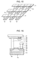
- FIG. 15 is an enlarged perspective view showing a simplified portion of a general MRAM.
- a read-out circuit portion is omitted for simplification, there are included, for example, 9 pieces of memory cells, and mutually intersecting bit lines 11 and writing word lines 12.
- a TMR element 10 is disposed. Writing to the TRM element 10 is carried out in such a manner that by passing a current through the bit line 11 and the write word line 12, and by using a synthetic magnetic field resulting from respective magnetic fields generated therefrom, an orientation of magnetization in the memory layer 2 in the TMR element 10 disposed at each intersection of the bit line 11 and the write word line 12 is caused to rotate parallel or anti-parallel relative to that in the magnetization pinned layer.
- An environment in which an MRAM is packaged and used is mainly on a high density packaging substrate, and inside electronics equipment. Although it depends on the types of electronic equipment, by recent developments of high density packaging techniques, there are densely packaged a variety of semiconductor elements, communication elements, a micro-motor and the like on a high density packaging substrate, and also antenna elements, various mechanical parts, power source and the like are densely packaged inside the electronic equipment thereby constructing a unit of equipment.
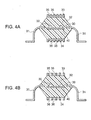
- MRAM magnetic shield structure of MRAM
- an insulating ferrite (MnZn ferrite and NiZn ferrite) layer as a passivation film of an MRAM element so as to provide a magnetic shielding characteristic (refer to USP No.5,902,690, specification (column 5) and drawings (FIG.1 & FIG.3)) .
- a high permeability magnetic body such as Permalloy on the top and bottom of the package so as to provide a magnetic shielding effect and prevent penetration of a magnetic flux into the internal element (refer to USP No. 5,939,772, specification column 2, FIGS. 1, 2).
- a structure of a shield lid made of a magnetic material such as soft iron or the like for cladding the element is disclosed (refer to Japanese Patent Application Publication No.2001-250206, right-hand column on page 5, FIG. 6).
Landscapes
- Engineering & Computer Science (AREA)
- Chemical & Material Sciences (AREA)
- Nanotechnology (AREA)
- Physics & Mathematics (AREA)
- Mathematical Physics (AREA)
- Theoretical Computer Science (AREA)
- Crystallography & Structural Chemistry (AREA)
- Mram Or Spin Memory Techniques (AREA)
- Hall/Mr Elements (AREA)
- Semiconductor Memories (AREA)
Applications Claiming Priority (3)
| Application Number | Priority Date | Filing Date | Title |
|---|---|---|---|
| JP2003006468A JP4013140B2 (ja) | 2003-01-15 | 2003-01-15 | 磁気メモリ装置 |
| JP2003006468 | 2003-01-15 | ||
| PCT/JP2003/016341 WO2004064149A1 (ja) | 2003-01-15 | 2003-12-19 | 磁気メモリ装置 |
Publications (2)
| Publication Number | Publication Date |
|---|---|
| EP1585172A1 true EP1585172A1 (de) | 2005-10-12 |
| EP1585172A4 EP1585172A4 (de) | 2008-10-08 |
Family
ID=32709074
Family Applications (1)
| Application Number | Title | Priority Date | Filing Date |
|---|---|---|---|
| EP03782844A Withdrawn EP1585172A4 (de) | 2003-01-15 | 2003-12-19 | Magnetspeicherbauteil |
Country Status (6)
| Country | Link |
|---|---|
| US (1) | US7119419B2 (de) |
| EP (1) | EP1585172A4 (de) |
| JP (1) | JP4013140B2 (de) |
| KR (1) | KR101019592B1 (de) |
| TW (1) | TWI231975B (de) |
| WO (1) | WO2004064149A1 (de) |
Families Citing this family (28)
| Publication number | Priority date | Publication date | Assignee | Title |
|---|---|---|---|---|
| EP1594163A1 (de) * | 2004-05-03 | 2005-11-09 | Commissariat A L'energie Atomique | Abgeschirmte elektrische Vorrichtung und sowie Herstellungsverfahren |
| JP4682585B2 (ja) * | 2004-11-01 | 2011-05-11 | ソニー株式会社 | 記憶素子及びメモリ |
| US7183617B2 (en) * | 2005-02-17 | 2007-02-27 | Taiwan Semiconductor Manufacturing Co., Ltd. | Magnetic shielding for magnetically sensitive semiconductor devices |
| CN101213429B (zh) * | 2005-06-27 | 2012-02-08 | Hl-平面技术有限公司 | 用于检测电磁波的器件以及生产这样的器件的方法 |
| JP5046189B2 (ja) | 2005-10-03 | 2012-10-10 | 日本電気株式会社 | 磁気ランダムアクセスメモリ |
| US7795708B2 (en) * | 2006-06-02 | 2010-09-14 | Honeywell International Inc. | Multilayer structures for magnetic shielding |
| US8269319B2 (en) * | 2006-10-13 | 2012-09-18 | Tessera, Inc. | Collective and synergistic MRAM shields |
| JP5062248B2 (ja) | 2007-02-27 | 2012-10-31 | ルネサスエレクトロニクス株式会社 | 磁気メモリチップ装置の製造方法 |
| US7968978B2 (en) * | 2007-06-14 | 2011-06-28 | Raytheon Company | Microwave integrated circuit package and method for forming such package |
| US8587297B2 (en) | 2007-12-04 | 2013-11-19 | Infineon Technologies Ag | Integrated circuit including sensor having injection molded magnetic material |
| JP5425461B2 (ja) | 2008-12-26 | 2014-02-26 | ルネサスエレクトロニクス株式会社 | 半導体装置およびその製造方法 |
| JP5470602B2 (ja) * | 2009-04-01 | 2014-04-16 | ルネサスエレクトロニクス株式会社 | 磁気記憶装置 |
| US8253210B2 (en) * | 2009-04-30 | 2012-08-28 | Infineon Technologies Ag | Semiconductor device including a magnetic sensor chip |
| US8125057B2 (en) * | 2009-07-07 | 2012-02-28 | Seagate Technology Llc | Magnetic shielding for integrated circuit |
| US8248840B2 (en) * | 2010-03-26 | 2012-08-21 | Qualcomm Incorporated | Magnetoresistive random access memory (MRAM) with integrated magnetic film enhanced circuit elements |
| JP5483281B2 (ja) * | 2010-03-31 | 2014-05-07 | ルネサスエレクトロニクス株式会社 | 半導体装置および半導体装置アセンブリ |
| JP2012109307A (ja) | 2010-11-15 | 2012-06-07 | Renesas Electronics Corp | 半導体装置及び半導体装置の製造方法 |
| US8415775B2 (en) | 2010-11-23 | 2013-04-09 | Honeywell International Inc. | Magnetic shielding for multi-chip module packaging |
| CN102623482A (zh) * | 2011-02-01 | 2012-08-01 | 飞思卡尔半导体公司 | Mram器件及其装配方法 |
| JP6122353B2 (ja) | 2013-06-25 | 2017-04-26 | ルネサスエレクトロニクス株式会社 | 半導体パッケージ |
| US9655253B2 (en) * | 2013-07-25 | 2017-05-16 | Cyntec Co., Ltd. | Method of fabrication of encapsulated electronics devices mounted on a redistribution layer |
| KR102444235B1 (ko) * | 2015-08-13 | 2022-09-16 | 삼성전자주식회사 | 자기 쉴딩층을 구비한 mram 소자와 반도체 패키지, 및 그들의 제조방법 |
| CN209658154U (zh) * | 2016-12-05 | 2019-11-19 | 株式会社村田制作所 | 电子元件 |
| JP6490130B2 (ja) * | 2017-03-24 | 2019-03-27 | Tdk株式会社 | 磁気センサ |
| US10427439B2 (en) | 2017-09-11 | 2019-10-01 | Apple Inc. | Substrate marking for sealing surfaces |
| US11211489B2 (en) * | 2017-12-27 | 2021-12-28 | Intel Corporation | Low resistance field-effect transistors and methods of manufacturing the same |
| US10951053B2 (en) | 2018-09-10 | 2021-03-16 | Apple Inc. | Portable electronic device |
| US12581865B2 (en) * | 2021-04-22 | 2026-03-17 | Taiwan Semiconductor Manufacturing Company, Ltd. | Manufacturing method of package with magnetic shielding structure |
Family Cites Families (12)
| Publication number | Priority date | Publication date | Assignee | Title |
|---|---|---|---|---|
| US5902690A (en) | 1997-02-25 | 1999-05-11 | Motorola, Inc. | Stray magnetic shielding for a non-volatile MRAM |
| US5939772A (en) | 1997-10-31 | 1999-08-17 | Honeywell Inc. | Shielded package for magnetic devices |
| JP2001176027A (ja) * | 1999-12-14 | 2001-06-29 | Nec Corp | 磁気抵抗効果ヘッド及びこれを用いた磁気記憶装置 |
| JP3593652B2 (ja) | 2000-03-03 | 2004-11-24 | 富士通株式会社 | 磁気ランダムアクセスメモリ装置 |
| EP1297533B1 (de) * | 2000-06-23 | 2008-08-27 | Nxp B.V. | Magnetischer speicher |
| US6515352B1 (en) * | 2000-09-25 | 2003-02-04 | Micron Technology, Inc. | Shielding arrangement to protect a circuit from stray magnetic fields |
| DE10103314C2 (de) | 2001-01-25 | 2003-05-22 | Infineon Technologies Ag | Halbleiterspeichereinrichtung |
| JP2003115578A (ja) * | 2001-10-05 | 2003-04-18 | Canon Inc | 不揮発固体磁気メモリ装置、該不揮発固体磁気メモリ装置の製造方法およびマルチ・チップ・パッケージ |
| JP2003124538A (ja) | 2001-10-16 | 2003-04-25 | Sony Corp | 情報記憶装置およびその情報記憶装置を実装した電子機器 |
| JP3879566B2 (ja) | 2002-04-03 | 2007-02-14 | ソニー株式会社 | 磁気不揮発性メモリ素子の磁気シールドパッケージおよび封止材料 |
| US6724027B2 (en) * | 2002-04-18 | 2004-04-20 | Hewlett-Packard Development Company, L.P. | Magnetic shielding for MRAM devices |
| US6808940B2 (en) * | 2002-08-30 | 2004-10-26 | Hewlett-Packard Development Company, L.P. | Magnetic shielding for reducing magnetic interference |
-
2003
- 2003-01-15 JP JP2003006468A patent/JP4013140B2/ja not_active Expired - Fee Related
- 2003-12-19 EP EP03782844A patent/EP1585172A4/de not_active Withdrawn
- 2003-12-19 US US10/506,752 patent/US7119419B2/en not_active Expired - Fee Related
- 2003-12-19 KR KR1020047014155A patent/KR101019592B1/ko not_active Expired - Fee Related
- 2003-12-19 WO PCT/JP2003/016341 patent/WO2004064149A1/ja not_active Ceased
- 2003-12-23 TW TW092136555A patent/TWI231975B/zh not_active IP Right Cessation
Also Published As
| Publication number | Publication date |
|---|---|
| KR101019592B1 (ko) | 2011-03-07 |
| TW200425426A (en) | 2004-11-16 |
| US7119419B2 (en) | 2006-10-10 |
| US20050116255A1 (en) | 2005-06-02 |
| WO2004064149A1 (ja) | 2004-07-29 |
| JP2004221288A (ja) | 2004-08-05 |
| KR20050096838A (ko) | 2005-10-06 |
| JP4013140B2 (ja) | 2007-11-28 |
| TWI231975B (en) | 2005-05-01 |
| EP1585172A4 (de) | 2008-10-08 |
Similar Documents
| Publication | Publication Date | Title |
|---|---|---|
| US7119419B2 (en) | Detailed description of the presently preferred embodiments | |
| JP4096302B2 (ja) | 磁気メモリ装置 | |
| US6970376B1 (en) | Magnetic random access memory and method of writing data in magnetic random access memory | |
| JP4444241B2 (ja) | 磁気抵抗効果素子、磁気ランダムアクセスメモリ、電子カード及び電子装置 | |
| CN100458968C (zh) | 磁存储装置 | |
| EP1096500B1 (de) | Magnetisierungssteuerungsverfahren und Datenspeicherungsvefahren | |
| JP5017347B2 (ja) | 磁気抵抗効果素子、磁気ランダムアクセスメモリ、電子カード、電子装置、磁気抵抗効果素子の製造方法、及び、磁気ランダムアクセスメモリの製造方法 | |
| US8258604B2 (en) | Semiconductor device and method of manufacturing same | |
| EP1575054B1 (de) | Magnetische Abschirmung und magnetische Speichervorrichtung | |
| JP3961914B2 (ja) | 磁気メモリ装置 | |
| JP2003115578A (ja) | 不揮発固体磁気メモリ装置、該不揮発固体磁気メモリ装置の製造方法およびマルチ・チップ・パッケージ | |
| JP2005158985A (ja) | 磁気メモリ装置の実装構造及び実装基板 | |
| JP4147466B2 (ja) | 磁気メモリ装置 | |
| JP2004221463A (ja) | 磁気メモリ装置 | |
| JP2004207322A (ja) | 磁気メモリ装置 | |
| JP2004193246A (ja) | 磁気メモリ装置 | |
| JP2004221289A (ja) | 磁気メモリ装置 | |
| JP2005203535A (ja) | 磁気メモリ |
Legal Events
| Date | Code | Title | Description |
|---|---|---|---|
| PUAI | Public reference made under article 153(3) epc to a published international application that has entered the european phase |
Free format text: ORIGINAL CODE: 0009012 |
|
| 17P | Request for examination filed |
Effective date: 20040913 |
|
| AK | Designated contracting states |
Kind code of ref document: A1 Designated state(s): AT BE BG CH CY CZ DE DK EE ES FI FR GB GR HU IE IT LI LU MC NL PT RO SE SI SK TR |
|
| RBV | Designated contracting states (corrected) |
Designated state(s): DE FR GB |
|
| A4 | Supplementary search report drawn up and despatched |
Effective date: 20080910 |
|
| 17Q | First examination report despatched |
Effective date: 20081223 |
|
| RIC1 | Information provided on ipc code assigned before grant |
Ipc: H01L 27/22 20060101ALI20100823BHEP Ipc: H01L 23/552 20060101AFI20100823BHEP |
|
| GRAP | Despatch of communication of intention to grant a patent |
Free format text: ORIGINAL CODE: EPIDOSNIGR1 |
|
| STAA | Information on the status of an ep patent application or granted ep patent |
Free format text: STATUS: THE APPLICATION IS DEEMED TO BE WITHDRAWN |
|
| 18D | Application deemed to be withdrawn |
Effective date: 20110326 |