EP1577959A2 - Halbleiter LED mit in der Ebene liegenden lichtemittierende Schichten - Google Patents
Halbleiter LED mit in der Ebene liegenden lichtemittierende Schichten Download PDFInfo
- Publication number
- EP1577959A2 EP1577959A2 EP05101808A EP05101808A EP1577959A2 EP 1577959 A2 EP1577959 A2 EP 1577959A2 EP 05101808 A EP05101808 A EP 05101808A EP 05101808 A EP05101808 A EP 05101808A EP 1577959 A2 EP1577959 A2 EP 1577959A2
- Authority
- EP
- European Patent Office
- Prior art keywords
- active region
- type region
- light
- region
- polarization
- Prior art date
- Legal status (The legal status is an assumption and is not a legal conclusion. Google has not performed a legal analysis and makes no representation as to the accuracy of the status listed.)
- Withdrawn
Links
Images



Classifications
-
- H—ELECTRICITY
- H10—SEMICONDUCTOR DEVICES; ELECTRIC SOLID-STATE DEVICES NOT OTHERWISE PROVIDED FOR
- H10H—INORGANIC LIGHT-EMITTING SEMICONDUCTOR DEVICES HAVING POTENTIAL BARRIERS
- H10H20/00—Individual inorganic light-emitting semiconductor devices having potential barriers, e.g. light-emitting diodes [LED]
- H10H20/80—Constructional details
- H10H20/81—Bodies
- H10H20/817—Bodies characterised by the crystal structures or orientations, e.g. polycrystalline, amorphous or porous
- H10H20/818—Bodies characterised by the crystal structures or orientations, e.g. polycrystalline, amorphous or porous within the light-emitting regions
-
- H—ELECTRICITY
- H10—SEMICONDUCTOR DEVICES; ELECTRIC SOLID-STATE DEVICES NOT OTHERWISE PROVIDED FOR
- H10H—INORGANIC LIGHT-EMITTING SEMICONDUCTOR DEVICES HAVING POTENTIAL BARRIERS
- H10H20/00—Individual inorganic light-emitting semiconductor devices having potential barriers, e.g. light-emitting diodes [LED]
- H10H20/80—Constructional details
- H10H20/81—Bodies
- H10H20/822—Materials of the light-emitting regions
- H10H20/824—Materials of the light-emitting regions comprising only Group III-V materials, e.g. GaP
- H10H20/825—Materials of the light-emitting regions comprising only Group III-V materials, e.g. GaP containing nitrogen, e.g. GaN
-
- H—ELECTRICITY
- H10—SEMICONDUCTOR DEVICES; ELECTRIC SOLID-STATE DEVICES NOT OTHERWISE PROVIDED FOR
- H10H—INORGANIC LIGHT-EMITTING SEMICONDUCTOR DEVICES HAVING POTENTIAL BARRIERS
- H10H20/00—Individual inorganic light-emitting semiconductor devices having potential barriers, e.g. light-emitting diodes [LED]
- H10H20/80—Constructional details
- H10H20/81—Bodies
- H10H20/814—Bodies having reflecting means, e.g. semiconductor Bragg reflectors
- H10H20/8142—Bodies having reflecting means, e.g. semiconductor Bragg reflectors forming resonant cavity structures
-
- H—ELECTRICITY
- H10—SEMICONDUCTOR DEVICES; ELECTRIC SOLID-STATE DEVICES NOT OTHERWISE PROVIDED FOR
- H10H—INORGANIC LIGHT-EMITTING SEMICONDUCTOR DEVICES HAVING POTENTIAL BARRIERS
- H10H20/00—Individual inorganic light-emitting semiconductor devices having potential barriers, e.g. light-emitting diodes [LED]
- H10H20/80—Constructional details
- H10H20/83—Electrodes
- H10H20/832—Electrodes characterised by their material
- H10H20/835—Reflective materials
-
- H—ELECTRICITY
- H10—SEMICONDUCTOR DEVICES; ELECTRIC SOLID-STATE DEVICES NOT OTHERWISE PROVIDED FOR
- H10H—INORGANIC LIGHT-EMITTING SEMICONDUCTOR DEVICES HAVING POTENTIAL BARRIERS
- H10H20/00—Individual inorganic light-emitting semiconductor devices having potential barriers, e.g. light-emitting diodes [LED]
- H10H20/80—Constructional details
- H10H20/84—Coatings, e.g. passivation layers or antireflective coatings
- H10H20/841—Reflective coatings, e.g. dielectric Bragg reflectors
-
- H—ELECTRICITY
- H10—SEMICONDUCTOR DEVICES; ELECTRIC SOLID-STATE DEVICES NOT OTHERWISE PROVIDED FOR
- H10H—INORGANIC LIGHT-EMITTING SEMICONDUCTOR DEVICES HAVING POTENTIAL BARRIERS
- H10H20/00—Individual inorganic light-emitting semiconductor devices having potential barriers, e.g. light-emitting diodes [LED]
- H10H20/80—Constructional details
- H10H20/872—Periodic patterns for optical field-shaping, e.g. photonic bandgap structures
-
- H—ELECTRICITY
- H10—SEMICONDUCTOR DEVICES; ELECTRIC SOLID-STATE DEVICES NOT OTHERWISE PROVIDED FOR
- H10W—GENERIC PACKAGES, INTERCONNECTIONS, CONNECTORS OR OTHER CONSTRUCTIONAL DETAILS OF DEVICES COVERED BY CLASS H10
- H10W90/00—Package configurations
Definitions
- the present invention relates to semiconductor light emitting devices that emit polarized light.
- LEDs light emitting diodes
- RCLEDs resonant cavity light emitting diodes
- VCSELs vertical cavity laser diodes
- edge emitting lasers are among the most efficient light sources currently available.
- Materials systems currently of interest in the manufacture of high-brightness light emitting devices capable of operation across the visible spectrum include Group III-V semiconductors, particularly binary, ternary, and quaternary alloys of gallium, aluminum, indium, and nitrogen, also referred to as III-nitride materials.
- III-nitride light emitting devices are fabricated by epitaxially growing a stack of semiconductor layers of different compositions and dopant concentrations on a sapphire, silicon carbide, III-nitride, or other suitable substrate by metal-organic chemical vapor deposition (MOCVD), molecular beam epitaxy (MBE), or other epitaxial techniques.
- MOCVD metal-organic chemical vapor deposition
- MBE molecular beam epitaxy
- the stack often includes one or more n-type layers doped with, for example, Si, formed over the substrate, a light emitting or active region formed over the n-type layer or layers, and one or more p-type layers doped with, for example, Mg, formed over the active region.
- One class of UV through green light emitting diodes or short wavelength laser diodes use InGaN/GaN or InGaN/InGaN strained quantum wells to generate light by the recombination of electrons and holes injected from the n- and p-type regions sandwiching the quantum wells.
- the crystal structure is wurtzite with two equivalent crystal axes in the plane of the quantum well and a third crystal axis, the ⁇ 0001> axis, perpendicular to the quantum well.
- Light emitted from such devices is observed to have no net polarization, meaning that any point (atom, molecule, or electron-hole pair) in the active region of such devices is observed to emit light with a polarization direction randomly and very quickly (typically less than 10 nanoseconds) changing in time so that no net polarization is observed over longer time scales.
- Such conventional structures are said to emit randomly polarized light.
- a semiconductor light emitting device includes a planar active region with a wurtzite crystal structure having a ⁇ 0001> axis roughly parallel to the plane of the layer, referred to as an in-plane polarized active region.
- the in-plane polarized active region may include, for example, a ⁇ 11 2 0 ⁇ or ⁇ 10 1 0 ⁇ InGaN light emitting layer.
- the emitted light polarization direction is both perpendicular to the ⁇ 0001> axis and parallel to the quantum well, thus much of the emitted light is of a single linear polarization state.
- a wire-grid contact serves as a polarizer oriented to transmit or reflect light of a polarization of the majority of light emitted from the active region.
- two active regions emitting the same or different colored light are separated by a polarizer oriented to pass polarized light emitted by the bottom active region, and to reflect cross-polarized light emitted by the top active region.
- a polarizer reflects light scattered by a wavelength converting layer.
- Fig. 1 illustrates a wurtzite crystal GaN structure.
- III-nitride devices are often grown on the ⁇ 0001 ⁇ or c-plane of a sapphire substrate, due to the wide availability and ease of handling such substrates.
- the resulting III-nitride layers, including the light emitting layer or layers in the active region, are typically ⁇ 0001 ⁇ layers, meaning the ⁇ 0001> axis is perpendicular to the plane of the III-nitride layers. Light emitted by such active regions typically shows no polarization preference when measured externally to the crystal.
- a III-nitride light emitting device is grown such that the crystallographic ⁇ 0001> direction is roughly parallel to the plane of the light emitting III-nitride layers.
- Light emitted by such devices may be at least partially linearly polarized.
- a device or crystal layer with the ⁇ 0001> direction parallel to the plane of the layer or layers is referred to below as an "in-plane” or “in-plane polarized” device or layer, since the c-axis is parallel to or in the plane of the device layers.
- the light emitting layer or layers in the active region of a III-nitride device are ⁇ 10 1 0> or ⁇ 11 2 0> layers of the quaternary alloy In x Al y Ga 1-x-y N (0 ⁇ x ⁇ 1, 0 ⁇ y ⁇ 1, x + y ⁇ 1).
- Devices with in-plane light emitting layers may be fabricated by growing the device layers on an in-plane growth substrate.
- substrates suitable for growth of an in-plane active region include the ⁇ 10 1 0 ⁇ and ⁇ 11 2 0 ⁇ surfaces of SiC of the 2H, 4H, or 6H polytypes; the ⁇ 10 1 2 ⁇ surface of sapphire; and the ⁇ 100 ⁇ surface of ⁇ -LiAlO 2 .
- the orientation of the deposited III-nitride films matches the orientation of the substrate.
- the process of depositing the in-plane III-nitride layers is similar to the process used for depositing ⁇ 0001> III-nitride layers on a ⁇ 0001> SiC substrate.
- a buffer layer of AlGaN is deposited, at high temperature ( ⁇ 1100°C), directly on the SiC substrate.
- a layer of GaN is deposited on the AlGaN buffer layer.
- Light-emitting AlInGaN quantum wells are deposited on the GaN layer.
- the deposited III-nitride films are oriented in the ⁇ 1120 > direction.
- the process of depositing in-plane III-nitride layers is similar to the process used for depositing ⁇ 0001> III-nitride layers on a ⁇ 0001> sapphire substrate.
- a III-nitride buffer layer is deposited, at low temperature ( ⁇ 550°C), directly on the sapphire substrate.
- a layer of GaN is deposited on the III-nitride buffer layer. Light emitting AlInGaN quantum wells are deposited on the GaN layer.
- the deposited III-nitride films are oriented in the ⁇ 10 1 0> direction.
- the process for depositing in-plane III-nitride layers by molecular beam epitaxy consists of depositing a III-nitride buffer layer at low temperature ( ⁇ 550°C) directly on the substrate, followed by a layer of GaN grown at a higher temperature. The light-emitting AlInGaN quantum wells are deposited on the GaN layer.
- the inventors prepared III-nitride photoluminescence test structures grown on ⁇ 10 1 0 ⁇ SiC and ⁇ 10 1 2 ⁇ sapphire.
- the test structures were excited by a 396 nm laser to emit light at 475 nm, the light from the ⁇ 10 1 0 ⁇ SiC device was greater than about 90% polarized, and the light from the ⁇ 10 1 2 ⁇ sapphire device was about 80% polarized.
- the test structures were electrically excited, the light from the ⁇ 10 1 0 ⁇ SiC device was 70-80% polarized.
- Percent polarization is defined as:
- Embodiments of the present invention may include devices that emit light that is at least 50% polarized.
- Unpolarized light consists of a very large number of photon emissions from a very large number of individual atoms, molecules, or electron-hole pairs. Each photon will have a random but a definite polarization direction and a train of such photons will be emitted at a very high rate, possibly greater than 100 million per second.
- Unpolarized light the sum total of the polarizations of every atom, molecule or electron-hole pair will sum up to zero when sampled over a time scale much larger than 1/100 millionth second. Unpolarized light is thus 0% polarized.
- Figs. 2-5 illustrate devices that combine an in-plane active region with a polarizer, which may act as a transparent or reflective electrical contact, depending on the orientation of the polarizer relative to the polarization of light emitted by the active region.
- Figs. 6 and 7 illustrate a photonic crystal device incorporating an in-plane active region.
- Figs. 8 and 10 illustrate a vertical cavity surface emitting laser and an edge-emitting laser incorporating an in-plane active region.
- Figs. 9A and 9B illustrate devices including an in-plane active region and a polarization-shifting surface such as a scattering surface or a birefringent layer.
- Figs. 2 and 3 are a cross-sectional view and a plan view of a first embodiment of the invention including an in-plane light emitting layer and a polarizer.
- In-plane active region 4 is sandwiched between an n-type region 2 and a p-type region 6.
- Each of n-type region 2, active region 4, and p-type region 6 may include multiple layers of different composition, dopant concentration, and thickness.
- Active region 4 may include multiple quantum wells separated by barrier layers.
- a reflective contact 8 attaches epitaxial regions 2, 4, and 6 to a host substrate 10.
- Contact 8 may include, for example, an ohmic contact layer, a reflective layer such as silver, a guard layer, and bonding layers to bond the epitaxial structure to the host substrate. Light is extracted from the device through n-type region 2.
- a polarizer 12 is formed on n-type region 2.
- the polarizer illustrated in Fig. 2 is a wire grid polarizer.
- Wire grid polarizers reflect photons of a polarization that is parallel to the wires, and transmit photons of a polarization that is perpendicular to the wires.
- Polarizer 12 is oriented to transmit photons of the polarization emitted by active region 4, and to reflect any photons of opposite polarization.
- the periodicity of wires in a wire grid polarizer may be optimized for the wavelength of emission of the device, resulting in high reflecting efficiency.
- the spacing and thickness of the wires may depend on the wavelength of light emitted by the device.
- the wires may be between about 10 nm and about 1000 nm thick and are usually between about 50 nm and about 80 nm thick.
- the wires may be spaced between about 10 nm and about 1000 nm apart and are usually between about 100 nm and about 200 nm apart.
- the wires may be, for example, single or multi-layer metal structures including, for example, one or more of an ohmic layer, a reflective layer, a guard layer, and a bonding layer. Examples of suitable materials include silver, aluminum, gold, and rhodium.
- Commercially available wire grid polarizers of dimensions within the ranges described above have been shown to have polarization selectivity to light with wavelengths over the range of 400-600 nm. The proper orientation of the wire grid polarizer may be selected based on the construction of the device, or by measuring the polarization of light emitted by the device.
- wire grid polarizer 12 serves as a contact to n-type region 2.
- the contact may be completed by forming pads electrically connected to wire grid polarizer 12 that are suitable for bonding to, for example, a submount or wire bonds.
- a polarizer oriented to pass light of the polarization emitted by the active region results in a contact that is transparent to the light emitted by the active region, reducing any absorption of light by the contact that would decrease the extraction efficiency of the device.
- a current spreading layer such as indium tin oxide may be disposed between the semiconductor layer (n-type region 2 in Fig. 2) and the polarizer.
- a wire grid polarizer may serve as a contact to p-type region 6.
- the wire grid polarizer permits the use of thin epitaxial layers in the device.
- the total thickness of regions 2, 4, and 6 may be between about 0.1 and about 1 micron thick. Thinning the epitaxial structure enhances light extraction from the device.
- the current spreading distance in p-type region 6 decreases, requiring a p-contact covering a large area, or requiring a closely-spaced grid or finger p-contact. If the p-contact absorbs light, the large area or closely spaced fingers required in a thin device may absorb a significant amount of light, reducing the efficiency of the device.
- in-plane polarized active region and a wire grid polarizer as a p-contact results in a device having a contact with fingers close enough to provide sufficient current to the device, but transparent to light emitted by the active region. Accordingly, in-plane active regions may permit thinner devices to be made without sacrificing light extraction.
- the device illustrated in Fig. 2 is fabricated by growing epitaxial regions 2, 4, and 6 on a growth substrate, depositing contact 8, then bonding the epitaxial structure to host substrate 10.
- the growth substrate may then be removed, for example by laser lift-off in the case of a sapphire substrate, or by etching in the case of a SiC substrate.
- the epitaxial structure may be thinned to a desired thickness.
- III-nitride devices by substrate removal is described in more detail in Application Serial No. [Attorney Docket Number LUM-03-05-01], filed March 19, 2004, and incorporated herein by reference.
- Polarizer 12 is often formed as the last processing step, prior to singulating the dice from the host substrate wafer.
- a wire grid polarizer may be formed by the following method: a layer of metal is deposited on the wafer, then patterned by, for example, depositing a layer of photoresist over the metal then patterning the photoresist by exposing it to radiation, for example by shining short-wavelength light through a photomask with the wire-grid polarizer pattern already formed on it, by using the interference pattern from two laser beams to project an array of lines of light of varying intensity onto the photoresist, or by drawing the wire-grid polarizer pattern on the photoresist with an electron beam.
- the wire grid polarizer pattern may be imprinted into a polymer layer with a master stamp containing the inverse of the desired pattern.
- the exposed metal layer is etched by chemicals (wet etching), a reactive ion beam (RIE), a plasma-enhanced reactive ion beam, an inductively-coupled plasma (ICP), or other appropriate technique known in the art.
- RIE reactive ion beam
- ICP inductively-coupled plasma
- the remaining photoresist or polymer may then be chemically stripped from the wafer, resulting in a pattern of parallel, evenly spaced metal lines 14 on the wafer, separated by spaces 16, as illustrated in Fig. 3.
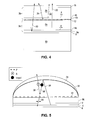
- Fig. 4 illustrates a second embodiment of the invention including an in-plane light emitting layer and a polarizer.
- Two epitaxial structures 3a and 3b are stacked and separated by polarizer 12, which may serve as an electrical contact and bonding layer between epitaxial structures 3a and 3b.
- Polarizer 12 may be a wire grid polarizer.
- the two active regions 4a and 4b emit light of orthogonal polarization.
- the bottom epitaxial structure 3a is bonded to a host substrate 10 by reflective contact 8. Light from both active regions is extracted from the device through the top of the n-type region 2b of the second epitaxial structure 3b.
- the structure and orientation of polarizer 12 is selected such that the polarized light emitted from the bottom active region 4a is transmitted, while the polarized light emitted from the top active region 4b is reflected.
- Light rays 20, 22, 24, and 26 demonstrate the behavior of the device of Fig. 4.
- Active region 4a primarily emits photons of polarization p.
- Active region 4b primarily emits photons of polarization s.
- Polarizer 12 transmits photons of polarization p and reflects photons of polarization s.
- Light ray 20 is emitted by active region 4a downward, toward contact 8.
- Light ray 20 is reflected by contact 8 and is incident on polarizer 12. Since light ray 20 has polarization p, it is transmitted by polarizer 12 and escapes through the top surface of the device.
- Light ray 22 is emitted by active region 4a toward polarizer 12, is transmitted by polarizer 12 since it is p-polarized, and escapes through the top surface of the device.
- Light ray 24 is emitted by active region 4b downward, toward polarizer 12. Since light ray 24 is s-polarized, it is reflected by polarizer 12 and escapes through the top surface of the device.
- Light ray 26 is emitted by active region 4b toward the top surface of the device, where it escapes.
- Polarizer 12 thus prevents light emitted downward by the top epitaxial structure 3b from being absorbed by bottom epitaxial structure 3a.
- the device illustrated in Fig. 4 may offer increased light output over a device with a single active region.
- the two active regions 4a and 4b may emit light of different wavelength. The wavelengths may be chosen such that the combined light emitted by the device appears white.
- the two epitaxial structures 3a and 3b may be formed from different materials systems, increasing the range of wavelengths available.
- the device illustrated in Fig. 4 may be fabricated by growing n-type region 2a, active region 4a, and p-type region 6a on a growth substrate, then forming contact 8, which may include, for example, ohmic contact layers, reflective layers, barrier layers, and bonding layers, on the surface of p-type region 6a.
- contact 8 which may include, for example, ohmic contact layers, reflective layers, barrier layers, and bonding layers, on the surface of p-type region 6a.
- Epitaxial structure 3a is then bonded to host substrate 10 and the growth substrate is removed.
- Polarizer 12 is then formed on the surface of n-type region 2a exposed by growth substrate removal.
- Polarizer 12 may serve as the electrical contact and bonding layer between epitaxial structure 3a and epitaxial structure 3b, or a separate metal or highly conductive layer may be formed on the surface of n-type region 2a to serve as a bonding layer and electrical contact between epitaxial structures 3a and 3b.
- Polarizer 12 may be formed from a soft metal suitable for bonding, such as silver.
- the second epitaxial structure is formed by growing n-type region 2b, active region 4b, and p-type region 6b on a growth substrate, then bonding the epitaxial structure to polarizer 12 such that the surface of p-type region 6b faces polarizer 12.
- the second growth substrate may then be removed and a second contact 18 formed on the exposed surface of n-type region 2b.
- Fig. 5 illustrates a third embodiment of the invention including an in-plane light emitting layer and a polarizer.
- N-type region 2, in-plane active region 4, and p-type region 6 are grown on a growth substrate 30.
- N- and p-contacts are both formed on the side of the epitaxial structure opposite the growth substrate, the n-contact by etching away a portion of active region 4 and p-type region 6 to expose a portion of n-type region 2.
- Light is extracted from the device though growth substrate 30.
- a polarizer 12 for example a wire grid polarizer, is formed on the surface of growth substrate 30.
- Polarizer 12 is structured and oriented to transmit light of the polarization emitted by active region 4 and reflect light of the opposite polarization.
- a wavelength converting material 32 is disposed in the path of light emitted from the device.
- Wavelength converting material 32 may be conformally deposited on substrate 30, for example by stenciling or electrophoretic deposition, disposed in a fill material deposited over substrate 30, or coated on a surface of or within the material forming a lens or cover 34 over the epitaxial structure.
- Wavelength converting material 32 may be a fluorescent material such as a phosphor or dye that absorbs light emitted by the active region and reemits light of a different wavelength. Wavelength converting material 32 emits light in all directions, meaning that a significant fraction of light emitted by wavelength converting material 32 is emitted towards growth substrate 30. Light emitted by wavelength converting material 32 is unpolarized. Accordingly, half of the fraction of light emitted by wavelength converting material 32 toward substrate 30 will be transmitted by polarizer 12 and half will be reflected. In contrast, in conventional devices, most of the light emitted toward the substrate is absorbed by growth substrate 30 or the epitaxial structure 3, reducing the extraction efficiency of the device. Light ray 36 illustrates this behavior.
- Light 36 is emitted from active region 6 with a polarization that is transmitted by polarizer 12.
- Light 36 is incident on wavelength converting layer 32, where it is absorbed and emitted toward substrate 30 as unpolarized, wavelength-converted light.
- wavelength converting layer 32 When light 36 is incident on polarizer 12, a portion is reflected back toward wavelength converting layer 32, where it has another chance to exit the device. A portion is transmitted into the growth substrate 30, where it may be absorbed or reflected such that is has another chance to escape the device.
- the device illustrated in Fig. 5 is a flip chip device that retains the growth substrate
- other types of devices including a thin device with the growth substrate removed as illustrated in Fig. 2, may combine a polarizer and a wavelength converting layer.
- Fig. 6 is a cross sectional view of a device including a photonic crystal and an in-plane active region.
- Photonic crystal 40 is created by forming a lattice of holes 42 separated by mesas 44 in n-type region 2 of the epitaxial structure 3.
- the lattice of holes creates a medium with a periodically modulated dielectric constant, affecting the way light propagates through the medium.
- the photons of the light emitting diode can be characterized by their spectrum or dispersion relation, describing the relation between the energy and the wavelength of the photons. The relationship may be plotted, yielding a photonic band diagram consisting of energy bands, or photonic bands, separated by band gaps.
- the photonic band diagram is similar to the spectrum of electrons in crystalline lattices as expressed in an electronic band diagram, the photonic band diagram is unrelated to the electronic band diagram.
- a photonic crystal When a photonic crystal is formed into a III-nitride LED it affects how light propagates in the structure. Therefore if the proper lattice spacing is chosen, light that would otherwise have been trapped in the structure by total internal reflection can now escape, increasing the extraction of the LED.
- alternative lattices can reduce the photon mode volume in the LED structure increasing the radiative rate or internal efficiency of the LED active layer.
- N-contact 46 may be formed on a region of n-type region 2 that is not textured with the photonic crystal, though in other embodiments n-contact 46 may be formed on the photonic crystal area of n-type region 2. Since the photonic crystal is formed in an n-type region, the n-type material (highly conductive) is able to laterally inject current from contact 46 to photonic crystal 40. Light is extracted from the device through photonic crystal 40, thus the arrangement of n-contact 46 is selected to maximize the area of the photonic crystal. For example, n-contact 46 may surround photonic crystal region 40. N-contact 46 is not limited to a ring contact but could also be a grid or other structure that facilitates proper current spreading.
- implantation can be used on the epitaxial material under n-contact 46, preventing current flow and light generation in that area.
- a reflective p-contact 8 is formed on p-type region 6.
- P-contact 8 connects the epitaxial structure 3 to a host substrate 10 either directly or via optional bonding layers.
- An optional contact (not shown) may be formed on the surface of host substrate 10 opposite the epitaxial structure 3.
- the photonic crystal structure can include a periodic variation of the thickness of n-type region 2, with alternating maxima and minima.
- An example is a grating (one-dimensional lattice) or the planar lattice of holes 42 described above (two-dimensional lattice).
- the lattice is characterized by the diameter of the holes, d, the lattice constant a, which measures the distance between the centers of nearest neighbor holes, the depth of the holes w, and the dielectric constant of the dielectric, disposed in the holes, ⁇ h .
- Parameters a, d, w, and ⁇ h influence the density of states of the bands, and in particular, the density of states at the band edges of the photonic crystal's spectrum. Parameters a, d, w, and ⁇ h thus influence the radiation pattern emitted by the device, and can be selected to enhance the extraction efficiency from the device.
- Holes 42 can be arranged to form triangular, square, hexagonal, honeycomb, or other well-known two-dimensional lattice types. In some embodiments, different lattice types are formed in different regions of the device. Holes 42 can have circular, square, hexagonal, or other cross sections. In some embodiments, the lattice spacing a is between about 0.1 ⁇ and about 10 ⁇ , preferably between about 0.1 ⁇ and about 4 ⁇ , where ⁇ is the wavelength in the device of light emitted by the active region. In some embodiments, holes 42 may have a diameter d between about 0.1 a and about 0.5 a, where a is the lattice constant. Holes 42 can be filled with air or with an optional dielectric (not shown) of dielectric constant ⁇ h , often between about 1 and about 16. Possible dielectrics include silicon oxides.
- an in-plane active region may simplify the structure of photonic crystal 40.
- Conventional active regions emit light of all polarizations, necessitating a photonic crystal structure that has band gaps for all polarizations of light
- the use of an in-plane active region emitting polarized light may permit the use of a much simpler lattice, since it is no longer necessary to control polarizations of light other than the polarization of light emitted from the active region. Accordingly, to achieve the same device performance, a simple line grating or square lattice may be all that is required for an in-plane active region device, instead of a triangular or hexagonal lattice that is difficult to fabricate.
- photonic crystal 40 is formed on a device with a thin epitaxial structure.
- the thickness of the epitaxial structure 3 is selected such that the epitaxial layers are as thin as possible to reduce the number of waveguided modes, but thick enough to efficiently spread current. In many embodiments, the thickness of epitaxial structure 3 is less than about 1 ⁇ m.
- the thickness of epitaxial structure 3 is between about ⁇ and about 5 ⁇ , between about 0.18 ⁇ m and about 0.94 ⁇ m for a device that emits 450 nm light.
- Holes 42 have a depth between about 0.05 ⁇ and the entire thickness of n-type region 2. Generally, holes 42 are formed entirely within n-type region 2 and do not penetrate into the active region. N-type region 2 usually has a thickness of about 0.1 microns or more. In general, the depth of holes 42 is selected to place the bottoms of holes 42 as close to the active region as possible without penetrating the active region.
- the radiation pattern emitted from the device can be tuned by changing the lattice type, distance between the active region and the photonic crystal, lattice parameter a, diameter d, and depth w.
- the lattice parameter a and diameter d are illustrated in the square lattice shown in Fig. 7.
- the radiation pattern may be adjusted to emit light preferentially in a chosen direction.
- photonic crystal 40 is entirely contained within n-type region 2.
- photonic crystal 40 may be formed in p-type region 6, or may extend from either p-type region 6 or n-type region 2 into or through active region 4.
- the simplified photonic crystal structure that may be possible with an in-plane active region may further improve the performance of the device by limiting the amount of active region that is etched away to form the photonic crystal, and by limiting the amount of etching done in the p-type region, which may damage the crystal and reduce device performance.
- Fig. 6 shows photonic crystal 40 on the surface of the device, in other embodiments, photonic crystal 40 may be formed in a region of the device that is not on the surface.
- a buried photonic crystal may be formed on one side of the active region, and a contact that acts as a polarizer, such as in the device illustrated in Fig. 2, may be formed on the opposite side of the active region on the surface of the device.
- III-nitride photonic crystal light emitting devices are described in more detail in Application Serial No. 10/059,588, "LED Efficiency Using Photonic Crystal Structure,” filed January 28, 2002 and Application Serial No. [Attorney Docket Number LUM-03-05-01], filed March 19, 2004, both of which are incorporated herein by reference.
- Fig. 8 is a cross sectional view of a vertical cavity surface emitting laser (VCSEL) incorporating an in-plane active region.
- Active region 4 is sandwiched between p-type region 6 and a first n-type region 2a.
- a tunnel junction 53 separates p-type region 6 from a second n-type region 2b.
- the cavity is formed by two mirrors 51 and 52, which may be, for example, dielectric distributed Bragg reflectors (DBRs).
- the cavity is connected to a host substrate 10 by contact 8, which is disposed between n-type region 2b and host 10.
- a second contact 18 is formed on n-type region 2a. Portions of layers 2a, 2b, 4, and 6 may be implanted with hydrogen to confine current within the region between mirrors 51 and 52.
- VCSELs require an adequate population inversion to provide an optical gain greater than the optical loss for the lasing mode. Any recombination process other than stimulated emission into the desired cavity modes tends to deplete the population inversion and limit efficiency.
- an example of an undesired mode is the mode that is degenerate but orthogonally polarized to the desired lasing mode.
- An in-plane active layer that emits light in a single polarization when operating below the lasing threshold will not support the orthogonally polarized mode, and will thus require fewer injected carriers to reach the lasing threshold.
- a VCSEL incorporating an in-plane active region may not exhibit polarization "flips" which are problematic for many applications such as displays that require light of a particular polarization.
- the device of Fig. 8 may be a resonant cavity device where one or both mirrors are less reflective than required for a VCSEL. Since the mirrors need not be as reflective for a resonant cavity device as for a VCSEL, in a resonant cavity device, the DBR shown in Fig. 8 as mirror 52 may be replaced with a metal mirror. Since a metal mirror is conductive, in a device with a metal mirror 52, n-type region 2b and tunnel junction 53 may be omitted from the device of Fig. 8. Examples of suitable metals include, for example, silver, gold, aluminum, and rhodium.
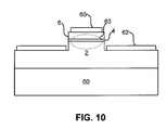
- in-plane active regions in laser structure described above in reference to Fig. 8 may also be applied to edge emitting laser diodes, such as the laser diode illustrated in Fig. 10.
- edge emitting laser diodes such as the laser diode illustrated in Fig. 10.
- the epitaxial layers are grown on a growth substrate 60, then the stack is etched to form a ridge structure whose vertical walls provide the waveguide.
- Parallel mirrors 63 are formed by cleaving or etching the ends of the waveguide to provide a reflecting surface.
- N-contacts 62 and p-contact 65 complete the structure.
- Figs. 9A and 9B illustrates devices including in-plane active regions and polarization shifting surfaces.
- the device of Fig. 9A includes a polarization-rotating layer 66.
- the device of Fig. 9B includes a polarization-randomizing layer 68.
- the devices shown in Figs. 9A and 9B are flip chip devices, where an n-type region 2, active region 4, and p-type region 6 are formed on a growth substrate 60. A portion of the p-type region and the active region is etched away to expose a portion of the n-type region, on which an n-contact 62 is deposited. Light is extracted from the device through growth substrate 60.
- the light emitted from the active region is linearly polarized perpendicular to the ⁇ 0001> axis.
- the III-nitride layers in the device preferentially absorb light that is polarized along this same direction. Consequently, the devices illustrated in Figs. 9A and 9B include a polarization shifting surface, either a polarization rotating layer 66 or a polarization randomizing surface 68, backed by a reflector 67 to reflect light back into the device. Light incident on the shifting surface would experience either a rotation or a randomization of its polarization, reducing the probability that the light will be reabsorbed.
- An example of a polarization randomizing structure 68 is a roughened scattering surface, either on the surface of the epitaxial structure (such as on the surface ofp-type region 6, as illustrated in Fig. 9B) or on the substrate side of the device.
- the surface may be roughened by selecting growth conditions to favor three dimensional growth or after growth by, for example, etching the surface or mechanically roughening the surface, such as with grinding grit.
- An example of polarization rotating structure 66 is a birefringent dielectric located between or adjacent to a metal contact and the epitaxial surface (such as adjacent to p-contact 64 and p-type region 6 as illustrated in Fig. 9A) or located on the substrate side of the device.
- p-contact 64 is formed as a plurality of evenly spaced metal lines, or as a grid. The thickness and spacing of p-contact sections 64 is chosen such that there is adequate current spreading in p-type region 6, but the surface of p-type region 6 covered by the polarization shifting structure is maximized.
- the textured region 68 or birefringent material 66 may have to be removed by etching.
- the polarization shifting structures illustrated in Figs. 9A and 9B may also be used in a thin film device such as the device illustrated in Fig. 2. In such devices, the polarization shifting structure may be disposed between host substrate 10 and p-type region 6.
Landscapes
- Led Devices (AREA)
- Polarising Elements (AREA)
- Semiconductor Lasers (AREA)
Applications Claiming Priority (2)
| Application Number | Priority Date | Filing Date | Title |
|---|---|---|---|
| US10/805,424 US7808011B2 (en) | 2004-03-19 | 2004-03-19 | Semiconductor light emitting devices including in-plane light emitting layers |
| US805424 | 2004-03-19 |
Publications (2)
| Publication Number | Publication Date |
|---|---|
| EP1577959A2 true EP1577959A2 (de) | 2005-09-21 |
| EP1577959A3 EP1577959A3 (de) | 2005-11-09 |
Family
ID=34838956
Family Applications (1)
| Application Number | Title | Priority Date | Filing Date |
|---|---|---|---|
| EP05101808A Withdrawn EP1577959A3 (de) | 2004-03-19 | 2005-03-09 | Halbleiter LED mit in der Ebene liegenden lichtemittierende Schichten |
Country Status (4)
| Country | Link |
|---|---|
| US (2) | US7808011B2 (de) |
| EP (1) | EP1577959A3 (de) |
| JP (1) | JP4713190B2 (de) |
| TW (1) | TW200541112A (de) |
Cited By (6)
| Publication number | Priority date | Publication date | Assignee | Title |
|---|---|---|---|---|
| DE102007032555A1 (de) * | 2007-07-12 | 2009-01-15 | Osram Opto Semiconductors Gmbh | Halbleiterchip und Verfahren zur Herstellung eines Halbleiterchips |
| WO2009039844A3 (de) * | 2007-09-28 | 2009-07-09 | Osram Opto Semiconductors Gmbh | Polarisierte strahlung emittierender halbleiterchip |
| DE102008030818A1 (de) * | 2008-06-30 | 2009-12-31 | Osram Opto Semiconductors Gmbh | Oberflächenemittierender Halbleiterlaser mit mehreren aktiven Zonen |
| EP1887634A3 (de) * | 2006-08-11 | 2011-09-07 | OSRAM Opto Semiconductors GmbH | Strahlungsemittierendes Halbleiterbauelement |
| WO2017205707A1 (en) * | 2016-05-27 | 2017-11-30 | The Government Of The United States Of America, As Represented By The Secretary Of The Navy | Resonant-cavity infrared photodetectors with fully-depleted absorbers |
| US10297699B2 (en) | 2016-05-27 | 2019-05-21 | The United States Of America, As Represented By The Secretary Of The Navy | In-plane resonant-cavity infrared photodetectors with fully-depleted absorbers |
Families Citing this family (105)
| Publication number | Priority date | Publication date | Assignee | Title |
|---|---|---|---|---|
| US7279718B2 (en) * | 2002-01-28 | 2007-10-09 | Philips Lumileds Lighting Company, Llc | LED including photonic crystal structure |
| US20030198837A1 (en) * | 2002-04-15 | 2003-10-23 | Craven Michael D. | Non-polar a-plane gallium nitride thin films grown by metalorganic chemical vapor deposition |
| US8809867B2 (en) * | 2002-04-15 | 2014-08-19 | The Regents Of The University Of California | Dislocation reduction in non-polar III-nitride thin films |
| WO2005064643A1 (en) * | 2003-04-15 | 2005-07-14 | The Regents Of The University Of California | NON-POLAR (A1,B,In,Ga)N QUANTUM WELLS |
| US7427555B2 (en) * | 2002-12-16 | 2008-09-23 | The Regents Of The University Of California | Growth of planar, non-polar gallium nitride by hydride vapor phase epitaxy |
| US7091661B2 (en) * | 2003-01-27 | 2006-08-15 | 3M Innovative Properties Company | Phosphor based light sources having a reflective polarizer |
| US7601223B2 (en) * | 2003-04-29 | 2009-10-13 | Asm International N.V. | Showerhead assembly and ALD methods |
| US7012279B2 (en) * | 2003-10-21 | 2006-03-14 | Lumileds Lighting U.S., Llc | Photonic crystal light emitting device |
| US7704763B2 (en) | 2003-12-09 | 2010-04-27 | The Regents Of The University Of California | Highly efficient group-III nitride based light emitting diodes via fabrication of structures on an N-face surface |
| US7285799B2 (en) * | 2004-04-21 | 2007-10-23 | Philip Lumileds Lighting Company, Llc | Semiconductor light emitting devices including in-plane light emitting layers |
| US7768023B2 (en) * | 2005-10-14 | 2010-08-03 | The Regents Of The University Of California | Photonic structures for efficient light extraction and conversion in multi-color light emitting devices |
| US7719020B2 (en) * | 2005-06-17 | 2010-05-18 | The Regents Of The University Of California | (Al,Ga,In)N and ZnO direct wafer bonded structure for optoelectronic applications, and its fabrication method |
| US6956246B1 (en) * | 2004-06-03 | 2005-10-18 | Lumileds Lighting U.S., Llc | Resonant cavity III-nitride light emitting devices fabricated by growth substrate removal |
| US7956360B2 (en) * | 2004-06-03 | 2011-06-07 | The Regents Of The University Of California | Growth of planar reduced dislocation density M-plane gallium nitride by hydride vapor phase epitaxy |
| US7781789B2 (en) * | 2006-11-15 | 2010-08-24 | The Regents Of The University Of California | Transparent mirrorless light emitting diode |
| US7582910B2 (en) * | 2005-02-28 | 2009-09-01 | The Regents Of The University Of California | High efficiency light emitting diode (LED) with optimized photonic crystal extractor |
| US8294166B2 (en) | 2006-12-11 | 2012-10-23 | The Regents Of The University Of California | Transparent light emitting diodes |
| US7345298B2 (en) * | 2005-02-28 | 2008-03-18 | The Regents Of The University Of California | Horizontal emitting, vertical emitting, beam shaped, distributed feedback (DFB) lasers by growth over a patterned substrate |
| US8860051B2 (en) | 2006-11-15 | 2014-10-14 | The Regents Of The University Of California | Textured phosphor conversion layer light emitting diode |
| US8227820B2 (en) | 2005-02-09 | 2012-07-24 | The Regents Of The University Of California | Semiconductor light-emitting device |
| JP4976849B2 (ja) * | 2004-07-12 | 2012-07-18 | ローム株式会社 | 半導体発光素子 |
| US7442964B2 (en) * | 2004-08-04 | 2008-10-28 | Philips Lumileds Lighting Company, Llc | Photonic crystal light emitting device with multiple lattices |
| US20060056024A1 (en) * | 2004-09-15 | 2006-03-16 | Ahn Seh W | Wire grid polarizer and manufacturing method thereof |
| US20060091412A1 (en) * | 2004-10-29 | 2006-05-04 | Wheatley John A | Polarized LED |
| JP4897210B2 (ja) * | 2004-11-18 | 2012-03-14 | ラピスセミコンダクタ株式会社 | 半導体装置の構造及びその製造方法 |
| JP4479535B2 (ja) * | 2005-02-21 | 2010-06-09 | セイコーエプソン株式会社 | 光学素子の製造方法 |
| US7291864B2 (en) * | 2005-02-28 | 2007-11-06 | The Regents Of The University Of California | Single or multi-color high efficiency light emitting diode (LED) by growth over a patterned substrate |
| US20060237735A1 (en) * | 2005-04-22 | 2006-10-26 | Jean-Yves Naulin | High-efficiency light extraction structures and methods for solid-state lighting |
| US9153645B2 (en) * | 2005-05-17 | 2015-10-06 | Taiwan Semiconductor Manufacturing Company, Ltd. | Lattice-mismatched semiconductor structures with reduced dislocation defect densities and related methods for device fabrication |
| TWI377602B (en) * | 2005-05-31 | 2012-11-21 | Japan Science & Tech Agency | Growth of planar non-polar {1-100} m-plane gallium nitride with metalorganic chemical vapor deposition (mocvd) |
| TWI397199B (zh) * | 2005-06-21 | 2013-05-21 | 獨立行政法人科學技術振興機構 | 用於製造經偏光發光二極體之封裝技術 |
| US8278128B2 (en) * | 2008-02-01 | 2012-10-02 | The Regents Of The University Of California | Enhancement of optical polarization of nitride light-emitting diodes by wafer off-axis cut |
| US20070096127A1 (en) * | 2005-08-26 | 2007-05-03 | Pattison P M | Semiconductor micro-cavity light emitting diode |
| JP5096671B2 (ja) * | 2005-09-13 | 2012-12-12 | 日立マクセルエナジー株式会社 | 密閉角形電池 |
| JP2009515344A (ja) | 2005-11-04 | 2009-04-09 | ザ リージェンツ オブ ザ ユニバーシティ オブ カリフォルニア | 高い光抽出効率の発光ダイオード(led) |
| WO2007065005A2 (en) * | 2005-12-02 | 2007-06-07 | The Regents Of University Of California | Improved horizontal emitting, vertical emitting, beam shaped, distributed feedback (dfb) lasers fabricated by growth over a patterned substrate with multiple overgrowth |
| WO2007067758A2 (en) * | 2005-12-08 | 2007-06-14 | The Regents Of The University Of California | High efficiency light emitting diode (led) |
| DE102006039369A1 (de) * | 2005-12-30 | 2007-07-05 | Osram Opto Semiconductors Gmbh | LED-Halbleiterkörper und Verwendung eines LED-Halbleiterkörpers |
| DE102006061167A1 (de) * | 2006-04-25 | 2007-12-20 | Osram Opto Semiconductors Gmbh | Optoelektronisches Halbleiterbauelement |
| KR20090018106A (ko) * | 2006-05-09 | 2009-02-19 | 더 리전츠 오브 더 유니버시티 오브 캘리포니아 | 비극성 및 준극성 (al, ga, in)n을 위한 인-시츄 결함 감소 기술 |
| KR100818451B1 (ko) * | 2006-07-03 | 2008-04-01 | 삼성전기주식회사 | 편광성을 갖는 반도체 발광 소자 |
| JP2008039655A (ja) * | 2006-08-09 | 2008-02-21 | National Institute Of Advanced Industrial & Technology | 微小対象物放出光検出装置 |
| JP4984119B2 (ja) | 2006-08-28 | 2012-07-25 | スタンレー電気株式会社 | 窒化物半導体結晶ないしそれを用いた発光素子及びその製造方法 |
| KR100809236B1 (ko) * | 2006-08-30 | 2008-03-05 | 삼성전기주식회사 | 편광 발광 다이오드 |
| JP5224310B2 (ja) * | 2006-08-31 | 2013-07-03 | 古河電気工業株式会社 | 垂直共振器型面発光レーザ |
| US7934194B2 (en) | 2006-10-17 | 2011-04-26 | The Mathworks, Inc. | User-defined hierarchies of user-defined classes of graphical objects in a graphical modeling environment |
| CA2669228C (en) * | 2006-11-15 | 2014-12-16 | The Regents Of The University Of California | Method for heteroepitaxial growth of high-quality n-face gan, inn, and ain and their alloys by metal organic chemical vapor deposition |
| US8193020B2 (en) | 2006-11-15 | 2012-06-05 | The Regents Of The University Of California | Method for heteroepitaxial growth of high-quality N-face GaN, InN, and AlN and their alloys by metal organic chemical vapor deposition |
| US7905605B2 (en) * | 2006-12-13 | 2011-03-15 | Koninklijke Philips Electronics N.V. | Multi-primary LED projection system |
| US8541869B2 (en) * | 2007-02-12 | 2013-09-24 | The Regents Of The University Of California | Cleaved facet (Ga,Al,In)N edge-emitting laser diodes grown on semipolar bulk gallium nitride substrates |
| JP4766704B2 (ja) * | 2007-04-20 | 2011-09-07 | キヤノン株式会社 | 面発光レーザ |
| US9046634B2 (en) * | 2007-06-14 | 2015-06-02 | Philips Lumileds Lighting Company, Llc | Thin flash or video recording light using low profile side emitting LED |
| JP5493252B2 (ja) * | 2007-06-28 | 2014-05-14 | 日亜化学工業株式会社 | 半導体発光素子 |
| DE102007053297A1 (de) * | 2007-09-13 | 2009-03-19 | Osram Opto Semiconductors Gmbh | Polarisierte Lichtquelle |
| US8399898B2 (en) * | 2007-10-25 | 2013-03-19 | Koninklijke Philips Electronics N.V. | Polarized light emitting device |
| KR20100097177A (ko) * | 2007-11-30 | 2010-09-02 | 더 리전트 오브 더 유니버시티 오브 캘리포니아 | 향상된 광 출력을 가지는 질화 갈륨 기반의 얇은 발광 다이오드 |
| JP2011511463A (ja) * | 2008-02-01 | 2011-04-07 | ザ リージェンツ オブ ザ ユニバーシティ オブ カリフォルニア | インジウム混和の増加による、窒化物発光ダイオードの偏光の向上 |
| JP2009239217A (ja) * | 2008-03-28 | 2009-10-15 | Nikon Corp | 発光ダイオード素子 |
| JP5167974B2 (ja) * | 2008-06-16 | 2013-03-21 | 豊田合成株式会社 | Iii族窒化物系化合物半導体発光素子及びその製造方法 |
| US8673074B2 (en) * | 2008-07-16 | 2014-03-18 | Ostendo Technologies, Inc. | Growth of planar non-polar {1 -1 0 0} M-plane and semi-polar {1 1 -2 2} gallium nitride with hydride vapor phase epitaxy (HVPE) |
| US8124996B2 (en) * | 2008-08-04 | 2012-02-28 | Soraa, Inc. | White light devices using non-polar or semipolar gallium containing materials and phosphors |
| JP5282503B2 (ja) | 2008-09-19 | 2013-09-04 | 日亜化学工業株式会社 | 半導体発光素子 |
| US8637331B2 (en) * | 2008-10-17 | 2014-01-28 | Bloominescence, Llc | Transparent polarized light-emitting device |
| KR101471859B1 (ko) * | 2008-11-27 | 2014-12-11 | 삼성전자주식회사 | 발광 다이오드 |
| DE102009020127B4 (de) * | 2009-03-25 | 2025-12-31 | OSRAM Opto Semiconductors Gesellschaft mit beschränkter Haftung | Leuchtdiode |
| US20140175377A1 (en) * | 2009-04-07 | 2014-06-26 | Soraa, Inc. | Polarized white light devices using non-polar or semipolar gallium containing materials and transparent phosphors |
| JP4975130B2 (ja) * | 2009-05-07 | 2012-07-11 | キヤノン株式会社 | フォトニック結晶面発光レーザ |
| DE102009023351A1 (de) * | 2009-05-29 | 2010-12-02 | Osram Opto Semiconductors Gmbh | Optoelektronischer Halbleiterchip und Verfahren zur Herstellung eines optoelektronischen Halbleiterchips |
| WO2010141943A1 (en) * | 2009-06-05 | 2010-12-09 | The Regents Of The University Of California | LONG WAVELENGTH NONPOLAR AND SEMIPOLAR (Al,Ga,In)N BASED LASER DIODES |
| US8933644B2 (en) | 2009-09-18 | 2015-01-13 | Soraa, Inc. | LED lamps with improved quality of light |
| US9293644B2 (en) | 2009-09-18 | 2016-03-22 | Soraa, Inc. | Power light emitting diode and method with uniform current density operation |
| WO2011048951A1 (ja) * | 2009-10-22 | 2011-04-28 | 日本電気株式会社 | 発光素子および該発光素子を用いた画像表示装置 |
| WO2011048952A1 (ja) * | 2009-10-22 | 2011-04-28 | 日本電気株式会社 | 発光素子および該発光素子を用いた画像表示装置 |
| US9028070B2 (en) | 2009-10-23 | 2015-05-12 | Nec Corporation | Light emitting element having structural bodies arrayed at a first pitch along a first direction and arrayed at a second pitch different from said first pitch along a second direction and projection display device provided with same |
| US8629065B2 (en) * | 2009-11-06 | 2014-01-14 | Ostendo Technologies, Inc. | Growth of planar non-polar {10-10} M-plane gallium nitride with hydride vapor phase epitaxy (HVPE) |
| US8779454B2 (en) | 2010-01-07 | 2014-07-15 | Nec Corporation | Light emitting element and image display device using the light emitting element |
| KR101667815B1 (ko) * | 2010-02-18 | 2016-10-19 | 엘지이노텍 주식회사 | 발광 소자, 발광 소자 제조방법 및 발광 소자 패키지 |
| JP2011249538A (ja) * | 2010-05-26 | 2011-12-08 | Sharp Corp | 発光装置および照明装置 |
| WO2012012409A2 (en) * | 2010-07-19 | 2012-01-26 | Rensselaer Polytechnic Institute | Integrated polarized light emitting diode with a built-in rotator |
| US8723160B2 (en) | 2010-07-28 | 2014-05-13 | SemiLEDs Optoelectronics Co., Ltd. | Light emitting diode (LED) die having peripheral electrode frame and method of fabrication |
| US8283652B2 (en) * | 2010-07-28 | 2012-10-09 | SemiLEDs Optoelectronics Co., Ltd. | Vertical light emitting diode (VLED) die having electrode frame and method of fabrication |
| CN103003963A (zh) * | 2010-08-06 | 2013-03-27 | 松下电器产业株式会社 | 半导体发光元件 |
| KR101441833B1 (ko) * | 2010-09-30 | 2014-09-18 | 도와 일렉트로닉스 가부시키가이샤 | Ⅲ족 질화물 반도체 발광소자 및 그 제조 방법 |
| EP2646744A4 (de) * | 2010-12-02 | 2014-07-09 | Intematix Corp | Feststofflampen mit einem lichtleiter- und photolumineszenz-material |
| KR20120092326A (ko) * | 2011-02-11 | 2012-08-21 | 서울옵토디바이스주식회사 | 광 결정 구조를 갖는 비극성 발광 다이오드 및 그것을 제조하는 방법 |
| US8552439B2 (en) * | 2011-04-07 | 2013-10-08 | Himax Display, Inc. | Light-emitting diode package |
| DE102011017196A1 (de) * | 2011-04-15 | 2012-10-18 | Osram Opto Semiconductors Gmbh | Polarisierte Strahlung emittierender Halbleiterchip |
| US9269858B2 (en) * | 2011-08-31 | 2016-02-23 | Micron Technology, Inc. | Engineered substrates for semiconductor devices and associated systems and methods |
| WO2013090177A1 (en) * | 2011-12-12 | 2013-06-20 | The Trustees Of Columbia University In The City Of New York | Systems and methods for suspended polymer photonic crystal cavities and waveguides |
| WO2013114483A1 (ja) * | 2012-02-01 | 2013-08-08 | パナソニック株式会社 | 窒化物半導体発光素子、その窒化物半導体発光素子を備えた光源及びその窒化物半導体発光素子の製造方法 |
| US9761763B2 (en) | 2012-12-21 | 2017-09-12 | Soraa, Inc. | Dense-luminescent-materials-coated violet LEDs |
| US9410664B2 (en) | 2013-08-29 | 2016-08-09 | Soraa, Inc. | Circadian friendly LED light source |
| WO2016103835A1 (ja) * | 2014-12-26 | 2016-06-30 | ソニー株式会社 | 光半導体デバイス |
| WO2017051443A1 (ja) * | 2015-09-24 | 2017-03-30 | ウシオ電機株式会社 | 露光方法、微細周期構造体の製造方法、グリッド偏光素子の製造方法及び露光装置 |
| US9595616B1 (en) * | 2015-12-02 | 2017-03-14 | Sandia Corporation | Vertical III-nitride thin-film power diode |
| WO2017127461A1 (en) * | 2016-01-18 | 2017-07-27 | Sensor Electronic Technology, Inc. | Semiconductor device with improved light propagation |
| DE102018105345A1 (de) * | 2018-03-08 | 2019-09-12 | RUHR-UNIVERSITäT BOCHUM | Vorrichtung zur Injektion spinpolarisierter Ladungsträger und zur Reflexion von Licht |
| US11417806B2 (en) * | 2018-07-30 | 2022-08-16 | Lumileds Llc | Dielectric mirror for broadband IR LEDs |
| CN111416276A (zh) * | 2019-01-08 | 2020-07-14 | 晶连股份有限公司 | 具有单一分散式布拉格反射器组的垂直共振腔面射型激光器 |
| JP7244745B2 (ja) * | 2019-02-15 | 2023-03-23 | 日亜化学工業株式会社 | 発光装置、及び、光学装置 |
| US11592166B2 (en) | 2020-05-12 | 2023-02-28 | Feit Electric Company, Inc. | Light emitting device having improved illumination and manufacturing flexibility |
| US11876042B2 (en) | 2020-08-03 | 2024-01-16 | Feit Electric Company, Inc. | Omnidirectional flexible light emitting device |
| CN113644058B (zh) * | 2021-08-11 | 2022-06-28 | 福建兆元光电有限公司 | 一种背光型Mini LED芯片及其制造方法 |
| JP2024110139A (ja) * | 2023-02-02 | 2024-08-15 | スタンレー電気株式会社 | 発光装置 |
| CN118825769B (zh) * | 2024-09-19 | 2024-12-20 | 中国科学院半导体研究所 | 侧向非晶硅光子晶体激光器、激光器阵列及制备方法 |
Family Cites Families (38)
| Publication number | Priority date | Publication date | Assignee | Title |
|---|---|---|---|---|
| US3599109A (en) * | 1969-04-16 | 1971-08-10 | Bell Telephone Labor Inc | Second photon visible emitting phosphor and device utilizing same |
| US4084130A (en) * | 1974-01-18 | 1978-04-11 | Texas Instruments Incorporated | Laser for integrated optical circuits |
| US4240692A (en) * | 1975-12-17 | 1980-12-23 | The University Of Chicago | Energy transmission |
| US4289381A (en) * | 1979-07-02 | 1981-09-15 | Hughes Aircraft Company | High selectivity thin film polarizer |
| EP0495301A1 (de) * | 1990-12-14 | 1992-07-22 | AT&T Corp. | Verfahren zur Herstellung eines Halbleiterlasers |
| JPH0763609A (ja) * | 1993-08-27 | 1995-03-10 | Minolta Co Ltd | 光シャッターを有する分光装置 |
| US6072197A (en) * | 1996-02-23 | 2000-06-06 | Fujitsu Limited | Semiconductor light emitting device with an active layer made of semiconductor having uniaxial anisotropy |
| JP3816176B2 (ja) * | 1996-02-23 | 2006-08-30 | 富士通株式会社 | 半導体発光素子及び光半導体装置 |
| JPH1022573A (ja) * | 1996-07-08 | 1998-01-23 | Canon Inc | 多重量子井戸半導体光デバイス |
| US5805624A (en) * | 1996-07-30 | 1998-09-08 | Hewlett-Packard Company | Long-wavelength infra-red vertical cavity surface-emitting laser on a gallium arsenide substrate |
| US5727108A (en) * | 1996-09-30 | 1998-03-10 | Troy Investments, Inc. | High efficiency compound parabolic concentrators and optical fiber powered spot luminaire |
| US5975703A (en) * | 1996-09-30 | 1999-11-02 | Digital Optics International | Image projection system |
| WO1998019375A1 (en) * | 1996-10-30 | 1998-05-07 | Hitachi, Ltd. | Optical information processor and semiconductor light emitting device suitable for the same |
| US5955749A (en) * | 1996-12-02 | 1999-09-21 | Massachusetts Institute Of Technology | Light emitting device utilizing a periodic dielectric structure |
| US6055262A (en) * | 1997-06-11 | 2000-04-25 | Honeywell Inc. | Resonant reflector for improved optoelectronic device performance and enhanced applicability |
| US6849472B2 (en) * | 1997-09-30 | 2005-02-01 | Lumileds Lighting U.S., Llc | Nitride semiconductor device with reduced polarization fields |
| JP3180743B2 (ja) * | 1997-11-17 | 2001-06-25 | 日本電気株式会社 | 窒化化合物半導体発光素子およびその製法 |
| US6273589B1 (en) * | 1999-01-29 | 2001-08-14 | Agilent Technologies, Inc. | Solid state illumination source utilizing dichroic reflectors |
| US6364487B1 (en) * | 1999-01-29 | 2002-04-02 | Agilent Technologies, Inc. | Solid state based illumination source for a projection display |
| US6320206B1 (en) * | 1999-02-05 | 2001-11-20 | Lumileds Lighting, U.S., Llc | Light emitting devices having wafer bonded aluminum gallium indium nitride structures and mirror stacks |
| US6257737B1 (en) * | 1999-05-20 | 2001-07-10 | Philips Electronics Na | Low-profile luminaire having a reflector for mixing light from a multi-color linear array of LEDs |
| US6122103A (en) * | 1999-06-22 | 2000-09-19 | Moxtech | Broadband wire grid polarizer for the visible spectrum |
| JP3511372B2 (ja) * | 1999-08-31 | 2004-03-29 | シャープ株式会社 | 半導体発光素子およびそれを使用した表示装置 |
| JP3791584B2 (ja) * | 1999-12-28 | 2006-06-28 | セイコーエプソン株式会社 | 面発光型半導体レーザおよび面発光型半導体レーザアレイ |
| US6603243B2 (en) * | 2000-03-06 | 2003-08-05 | Teledyne Technologies Incorporated | LED light source with field-of-view-controlling optics |
| WO2001093387A2 (en) | 2000-05-31 | 2001-12-06 | Sandia Corporation | Long wavelength vertical cavity surface emitting laser |
| US6853663B2 (en) * | 2000-06-02 | 2005-02-08 | Agilent Technologies, Inc. | Efficiency GaN-based light emitting devices |
| JP2002022981A (ja) * | 2000-07-05 | 2002-01-23 | Nec Corp | フォトニック結晶多層基板およびその製造方法 |
| US6611543B2 (en) * | 2000-12-23 | 2003-08-26 | Applied Optoelectronics, Inc. | Vertical-cavity surface-emitting laser with metal mirror and method of fabrication of same |
| JP4011292B2 (ja) * | 2001-01-15 | 2007-11-21 | 株式会社日立製作所 | 発光素子、及び表示装置 |
| US6930737B2 (en) * | 2001-01-16 | 2005-08-16 | Visteon Global Technologies, Inc. | LED backlighting system |
| US6897916B2 (en) * | 2001-09-11 | 2005-05-24 | Nitto Denko Corporation | Polarizing plate, optical element, and liquid crystal display |
| US6560265B2 (en) * | 2001-09-11 | 2003-05-06 | Applied Optoelectronics, Inc. | Method and apparatus for polarizing light in a VCSEL |
| US6739723B1 (en) * | 2001-12-07 | 2004-05-25 | Delta Electronics, Inc. | Polarization recapture system for liquid crystal-based data projectors |
| US20030198837A1 (en) * | 2002-04-15 | 2003-10-23 | Craven Michael D. | Non-polar a-plane gallium nitride thin films grown by metalorganic chemical vapor deposition |
| US6648475B1 (en) * | 2002-05-20 | 2003-11-18 | Eastman Kodak Company | Method and apparatus for increasing color gamut of a display |
| US6829281B2 (en) * | 2002-06-19 | 2004-12-07 | Finisar Corporation | Vertical cavity surface emitting laser using photonic crystals |
| JP4074498B2 (ja) * | 2002-09-25 | 2008-04-09 | セイコーエプソン株式会社 | 面発光型発光素子、光モジュールおよび光伝達装置 |
-
2004
- 2004-03-19 US US10/805,424 patent/US7808011B2/en not_active Expired - Fee Related
-
2005
- 2005-03-09 EP EP05101808A patent/EP1577959A3/de not_active Withdrawn
- 2005-03-16 TW TW094107957A patent/TW200541112A/zh unknown
- 2005-03-22 JP JP2005082235A patent/JP4713190B2/ja not_active Expired - Fee Related
-
2010
- 2010-05-18 US US12/781,935 patent/US20100226404A1/en not_active Abandoned
Cited By (15)
| Publication number | Priority date | Publication date | Assignee | Title |
|---|---|---|---|---|
| EP1887634A3 (de) * | 2006-08-11 | 2011-09-07 | OSRAM Opto Semiconductors GmbH | Strahlungsemittierendes Halbleiterbauelement |
| US8354682B2 (en) | 2006-08-11 | 2013-01-15 | Osram Opto Semiconductors Gmbh | Radiation emitting element |
| US7994519B2 (en) | 2007-07-12 | 2011-08-09 | Osram Opto Semiconductors Gmbh | Semiconductor chip and method for producing a semiconductor chip |
| DE102007032555A1 (de) * | 2007-07-12 | 2009-01-15 | Osram Opto Semiconductors Gmbh | Halbleiterchip und Verfahren zur Herstellung eines Halbleiterchips |
| WO2009039844A3 (de) * | 2007-09-28 | 2009-07-09 | Osram Opto Semiconductors Gmbh | Polarisierte strahlung emittierender halbleiterchip |
| DE102008030818B4 (de) | 2008-06-30 | 2022-03-03 | OSRAM Opto Semiconductors Gesellschaft mit beschränkter Haftung | Oberflächenemittierender Halbleiterlaser mit mehreren aktiven Zonen |
| DE102008030818A1 (de) * | 2008-06-30 | 2009-12-31 | Osram Opto Semiconductors Gmbh | Oberflächenemittierender Halbleiterlaser mit mehreren aktiven Zonen |
| WO2017205707A1 (en) * | 2016-05-27 | 2017-11-30 | The Government Of The United States Of America, As Represented By The Secretary Of The Navy | Resonant-cavity infrared photodetectors with fully-depleted absorbers |
| US10297699B2 (en) | 2016-05-27 | 2019-05-21 | The United States Of America, As Represented By The Secretary Of The Navy | In-plane resonant-cavity infrared photodetectors with fully-depleted absorbers |
| US10333011B2 (en) | 2016-05-27 | 2019-06-25 | The United States Of America, As Represented By The Secretary Of The Navy | In-plane resonant cavity infrared photodetectors with fully depleted absorbers |
| US10446701B2 (en) | 2016-05-27 | 2019-10-15 | The Government Of The United States Of America, As Represented By The Secretary Of The Navy | In-plane resonant-cavity infrared photodetectors with fully-depleted absorbers |
| US10453977B2 (en) | 2016-05-27 | 2019-10-22 | The Governement Of The United States Of America, As Represented By The Secretary Of The Navy | In-plane resonant-cavity infrared photodetectors with fully-depleted absorbers |
| US10461202B2 (en) | 2016-05-27 | 2019-10-29 | The Government Of The United States Of America, As Represented By The Secretary Of The Navy | In-plane resonant-cavity infrared photodetectors with fully-depleted absorbers |
| US10559704B2 (en) | 2016-05-27 | 2020-02-11 | The Government Of The United States Of America, As Represented By The Secretary Of The Navy | In-plane resonant-cavity infrared photodetectors with fully-depleted absorbers |
| US10062794B2 (en) | 2016-05-27 | 2018-08-28 | The United States Of America, As Represented By The Secretary Of The Navy | Resonant-cavity infrared photodetectors with fully-depleted absorbers |
Also Published As
| Publication number | Publication date |
|---|---|
| US7808011B2 (en) | 2010-10-05 |
| US20100226404A1 (en) | 2010-09-09 |
| JP4713190B2 (ja) | 2011-06-29 |
| TW200541112A (en) | 2005-12-16 |
| JP2005268809A (ja) | 2005-09-29 |
| US20050205884A1 (en) | 2005-09-22 |
| EP1577959A3 (de) | 2005-11-09 |
Similar Documents
| Publication | Publication Date | Title |
|---|---|---|
| US7808011B2 (en) | Semiconductor light emitting devices including in-plane light emitting layers | |
| US6847057B1 (en) | Semiconductor light emitting devices | |
| KR101424312B1 (ko) | 반도체칩 및 반도체칩의 제조 방법 | |
| US10062821B2 (en) | Light-emitting device | |
| JP4907842B2 (ja) | 平面全方位リフレクタを有する発光ダイオード | |
| US7294862B2 (en) | Photonic crystal light emitting device | |
| JP5237286B2 (ja) | フォトニック結晶により定められたアレイ状エミッタを含む発光デバイス | |
| RU2491682C2 (ru) | Полупроводниковое светоизлучающее устройство со структурами вывода света | |
| US9252330B2 (en) | Semiconductor light emitting element | |
| CN101655192B (zh) | 发光装置 | |
| KR101370257B1 (ko) | 광전자 반도체 소자 | |
| US20110241045A1 (en) | High efficiency light emitting diode and method for fabricating the same | |
| US20040113156A1 (en) | Semiconductor light emitting device and method for fabricating the same | |
| US20080179606A1 (en) | Nitride semiconductor light emitting device | |
| US10868213B2 (en) | LED utilizing internal color conversion with light extraction enhancements | |
| JP2003110136A (ja) | 発光素子 | |
| KR20070081184A (ko) | 질화물계 반도체 발광소자 및 그 제조방법 | |
| JP6924836B2 (ja) | 光電子半導体チップ | |
| WO2020005827A1 (en) | Led utilizing internal color conversion with light extraction enhancements | |
| JP2005276899A (ja) | 発光素子 | |
| JP4833537B2 (ja) | 半導体発光素子 | |
| US7242025B2 (en) | Radiation emitting semiconductor component having a nitride compound semiconductor body and a contact metallization layer on its surface | |
| JP2004014725A (ja) | 半導体発光素子 | |
| KR20080028292A (ko) | 경사진 측벽 반사면을 갖는 ⅲ―니트라이드계 led 구조및 그 제조방법 | |
| KR20080058722A (ko) | 다수의 절연층이 적층된 산란 중심을 구비하는 발광 소자제조방법 및 그 발광 소자 |
Legal Events
| Date | Code | Title | Description |
|---|---|---|---|
| PUAI | Public reference made under article 153(3) epc to a published international application that has entered the european phase |
Free format text: ORIGINAL CODE: 0009012 |
|
| AK | Designated contracting states |
Kind code of ref document: A2 Designated state(s): AT BE BG CH CY CZ DE DK EE ES FI FR GB GR HU IE IS IT LI LT LU MC NL PL PT RO SE SI SK TR |
|
| AX | Request for extension of the european patent |
Extension state: AL BA HR LV MK YU |
|
| PUAL | Search report despatched |
Free format text: ORIGINAL CODE: 0009013 |
|
| AK | Designated contracting states |
Kind code of ref document: A3 Designated state(s): AT BE BG CH CY CZ DE DK EE ES FI FR GB GR HU IE IS IT LI LT LU MC NL PL PT RO SE SI SK TR |
|
| AX | Request for extension of the european patent |
Extension state: AL BA HR LV MK YU |
|
| 17P | Request for examination filed |
Effective date: 20060509 |
|
| AKX | Designation fees paid |
Designated state(s): DE |
|
| RAP1 | Party data changed (applicant data changed or rights of an application transferred) |
Owner name: PHILIPS LUMILEDS LIGHTING COMPANY LLC |
|
| STAA | Information on the status of an ep patent application or granted ep patent |
Free format text: STATUS: THE APPLICATION HAS BEEN WITHDRAWN |
|
| 18W | Application withdrawn |
Effective date: 20121022 |