EP1566815A2 - Mehrleiterkabel und dessen Herstellungsverfahren. - Google Patents
Mehrleiterkabel und dessen Herstellungsverfahren. Download PDFInfo
- Publication number
- EP1566815A2 EP1566815A2 EP05250922A EP05250922A EP1566815A2 EP 1566815 A2 EP1566815 A2 EP 1566815A2 EP 05250922 A EP05250922 A EP 05250922A EP 05250922 A EP05250922 A EP 05250922A EP 1566815 A2 EP1566815 A2 EP 1566815A2
- Authority
- EP
- European Patent Office
- Prior art keywords
- wire
- cable
- wires
- multiconductor cable
- length
- Prior art date
- Legal status (The legal status is an assumption and is not a legal conclusion. Google has not performed a legal analysis and makes no representation as to the accuracy of the status listed.)
- Withdrawn
Links
- 238000000034 method Methods 0.000 title claims abstract description 14
- 230000001131 transforming effect Effects 0.000 claims description 15
- 239000004020 conductor Substances 0.000 description 8
- 239000004973 liquid crystal related substance Substances 0.000 description 5
- 239000002390 adhesive tape Substances 0.000 description 4
- 230000001413 cellular effect Effects 0.000 description 4
- 238000010586 diagram Methods 0.000 description 4
- 239000004698 Polyethylene Substances 0.000 description 1
- 239000000853 adhesive Substances 0.000 description 1
- 230000001070 adhesive effect Effects 0.000 description 1
- 238000005452 bending Methods 0.000 description 1
- 238000005352 clarification Methods 0.000 description 1
- 238000012986 modification Methods 0.000 description 1
- 230000004048 modification Effects 0.000 description 1
- 239000004033 plastic Substances 0.000 description 1
- 229920003023 plastic Polymers 0.000 description 1
- -1 polyethylene Polymers 0.000 description 1
- 229920000573 polyethylene Polymers 0.000 description 1
- 238000005096 rolling process Methods 0.000 description 1
- 238000012360 testing method Methods 0.000 description 1
- 238000012795 verification Methods 0.000 description 1
Images




Classifications
-
- H—ELECTRICITY
- H01—ELECTRIC ELEMENTS
- H01B—CABLES; CONDUCTORS; INSULATORS; SELECTION OF MATERIALS FOR THEIR CONDUCTIVE, INSULATING OR DIELECTRIC PROPERTIES
- H01B13/00—Apparatus or processes specially adapted for manufacturing conductors or cables
- H01B13/0036—Details
-
- H—ELECTRICITY
- H01—ELECTRIC ELEMENTS
- H01B—CABLES; CONDUCTORS; INSULATORS; SELECTION OF MATERIALS FOR THEIR CONDUCTIVE, INSULATING OR DIELECTRIC PROPERTIES
- H01B7/00—Insulated conductors or cables characterised by their form
- H01B7/08—Flat or ribbon cables
- H01B7/0892—Flat or ribbon cables incorporated in a cable of non-flat configuration
-
- H—ELECTRICITY
- H01—ELECTRIC ELEMENTS
- H01B—CABLES; CONDUCTORS; INSULATORS; SELECTION OF MATERIALS FOR THEIR CONDUCTIVE, INSULATING OR DIELECTRIC PROPERTIES
- H01B7/00—Insulated conductors or cables characterised by their form
- H01B7/08—Flat or ribbon cables
- H01B7/0838—Parallel wires, sandwiched between two insulating layers
-
- Y—GENERAL TAGGING OF NEW TECHNOLOGICAL DEVELOPMENTS; GENERAL TAGGING OF CROSS-SECTIONAL TECHNOLOGIES SPANNING OVER SEVERAL SECTIONS OF THE IPC; TECHNICAL SUBJECTS COVERED BY FORMER USPC CROSS-REFERENCE ART COLLECTIONS [XRACs] AND DIGESTS
- Y10—TECHNICAL SUBJECTS COVERED BY FORMER USPC
- Y10T—TECHNICAL SUBJECTS COVERED BY FORMER US CLASSIFICATION
- Y10T29/00—Metal working
- Y10T29/49—Method of mechanical manufacture
- Y10T29/49002—Electrical device making
- Y10T29/49117—Conductor or circuit manufacturing
- Y10T29/49174—Assembling terminal to elongated conductor
-
- Y—GENERAL TAGGING OF NEW TECHNOLOGICAL DEVELOPMENTS; GENERAL TAGGING OF CROSS-SECTIONAL TECHNOLOGIES SPANNING OVER SEVERAL SECTIONS OF THE IPC; TECHNICAL SUBJECTS COVERED BY FORMER USPC CROSS-REFERENCE ART COLLECTIONS [XRACs] AND DIGESTS
- Y10—TECHNICAL SUBJECTS COVERED BY FORMER USPC
- Y10T—TECHNICAL SUBJECTS COVERED BY FORMER US CLASSIFICATION
- Y10T29/00—Metal working
- Y10T29/49—Method of mechanical manufacture
- Y10T29/49002—Electrical device making
- Y10T29/49117—Conductor or circuit manufacturing
- Y10T29/49194—Assembling elongated conductors, e.g., splicing, etc.
-
- Y—GENERAL TAGGING OF NEW TECHNOLOGICAL DEVELOPMENTS; GENERAL TAGGING OF CROSS-SECTIONAL TECHNOLOGIES SPANNING OVER SEVERAL SECTIONS OF THE IPC; TECHNICAL SUBJECTS COVERED BY FORMER USPC CROSS-REFERENCE ART COLLECTIONS [XRACs] AND DIGESTS
- Y10—TECHNICAL SUBJECTS COVERED BY FORMER USPC
- Y10T—TECHNICAL SUBJECTS COVERED BY FORMER US CLASSIFICATION
- Y10T29/00—Metal working
- Y10T29/51—Plural diverse manufacturing apparatus including means for metal shaping or assembling
- Y10T29/5187—Wire working
-
- Y—GENERAL TAGGING OF NEW TECHNOLOGICAL DEVELOPMENTS; GENERAL TAGGING OF CROSS-SECTIONAL TECHNOLOGIES SPANNING OVER SEVERAL SECTIONS OF THE IPC; TECHNICAL SUBJECTS COVERED BY FORMER USPC CROSS-REFERENCE ART COLLECTIONS [XRACs] AND DIGESTS
- Y10—TECHNICAL SUBJECTS COVERED BY FORMER USPC
- Y10T—TECHNICAL SUBJECTS COVERED BY FORMER US CLASSIFICATION
- Y10T29/00—Metal working
- Y10T29/53—Means to assemble or disassemble
- Y10T29/5313—Means to assemble electrical device
- Y10T29/53261—Means to align and advance work part
-
- Y—GENERAL TAGGING OF NEW TECHNOLOGICAL DEVELOPMENTS; GENERAL TAGGING OF CROSS-SECTIONAL TECHNOLOGIES SPANNING OVER SEVERAL SECTIONS OF THE IPC; TECHNICAL SUBJECTS COVERED BY FORMER USPC CROSS-REFERENCE ART COLLECTIONS [XRACs] AND DIGESTS
- Y10—TECHNICAL SUBJECTS COVERED BY FORMER USPC
- Y10T—TECHNICAL SUBJECTS COVERED BY FORMER US CLASSIFICATION
- Y10T29/00—Metal working
- Y10T29/53—Means to assemble or disassemble
- Y10T29/5313—Means to assemble electrical device
- Y10T29/53265—Means to assemble electrical device with work-holder for assembly
Definitions
- the present invention relates to a multiconductor cable incorporating a plurality of insulated wires, coaxial conductors, or the like and a method of producing the multiconductor cable, particularly to a multiconductor cable in which a plurality of wires and conductors are tied together in a bundle at the intermediate portion and are arranged in a flat array at both ends, where the cable is provided with connectors or similar components, and a method of producing the multiconductor cable.
- connection between the main body of a device and a liquid crystal display and wiring in a device are made using extremely fine insulated wires and shielded wires including coaxial conductors.
- a multiconductor cable in which the foregoing wires and conductors are bound together is also used because it facilitates the wiring.
- a multiconductor cable is electrically connected through a connector having the shape of a card-edge connector in which a multitude of contacts are arranged in a row (such a connector is used for the connection of a printed circuit, for example).
- FIG. 6A is a plan view of an example of the conventional multiconductor cable
- Fig. 6B is a plan view of another example of the conventional multiconductor cable.
- a multiconductor cable 1a provided with connectors as shown in Fig. 6A is used, in which a plurality of electric wires 2 are arranged in parallel with a constant pitch to form a unified structure as a multiconductor cable.
- the cable 1a is suitable for the wiring along the inside wall of a device.
- a hinged portion such as the connection between the main body and a liquid crystal display of a cellular mobile phone
- its twisting property is insufficient at the hinged portion.
- the size of the hinged portion is small, the stress applied to the cable 1a is large and, consequently, the cable tends to suffer a break. Therefore, this type of cable is not suitable for use at a small-hinged portion.
- the wiring through a turning portion is made using a multiconductor cable 1b provided with connectors as shown in Fig. 6B.
- a multiconductor cable 1b provided with connectors as shown in Fig. 6B.
- both ends to which electrical connectors 3 are connected have a structure in which a plurality of wires 2 are arranged in a flat array and the intermediate portion has a structure in which the wires 2 are bundled together.
- the cable 1b may be produced such that only both ends have a flat shape and the intermediate portion is formed by bundling the intermediate portions of a plurality of disorganized wires.
- the cable 1b may also be produced by rolling up the intermediate portion of a plurality of wires that arranged in a flat array throughout the length.
- a plurality of wires 2 are bundled using a bundling member 4 having the shape of a tape.
- a bundling member 4 having the shape of a tape.
- an intermediate portion of the multiconductor cable is sometimes provided with a grounding member 5 for connecting that portion to the ground.
- the multiconductor cable 1b composed of a plurality of wires 2 having the same length
- wires placed in the middle position of a flat array are slackened and wires placed at the outside positions are pulled.
- the wires placed at the outside positions tend to break.
- the published Japanese patent applications Tokukoushou 61-230208 and Tokukai 2000-294045 have disclosed a multiconductor cable having a specific structure (see Fig. 4 of Tokukai 2000-294045).
- a wire placed at an outer position has a length longer than that of a wire placed at an inner position so that the slack and tension can be prevented.
- the length E is small to the extent that the ratio E/D is less than six, a problem is caused due to the difference in length between the minimum length of the wire placed at the center of the bundle and the maximum length of the wire placed at the outermost position of the bundle. More specifically, at the time of bundling a plurality of wires arranged in a flat array, even when the length of wires to be placed at the outer side and to undergo tension is simply increased, a wire having an excess length tends to buckle or break. In addition, for the use in a turning portion, if no consideration is given to the twisting, a break of wire cannot be prevented, that is, the problem cannot be totally solved.
- An object of the present invention is to offer a multiconductor cable that is reduced in the possibility of break even for use at a place where the cable undergoes twisting and a method capable of producing the multiconductor cable easily at a low cost.
- the present invention offers a multiconductor cable that incorporates a plurality of wires that:
- the multiconductor cable may satisfy the following formulae: ⁇ ⁇ 45 degrees, and (Lm - Ls) ⁇ 3 ⁇ ⁇ 2D(2 1/2 -1) ⁇ ⁇ 2.5D, where ⁇ is the angle produced by a wire's portion from one of the ends to the intermediate portion and the same wire's portion in the intermediate portion, Lm is the maximum length, Ls is the minimum length, and D is the width of the cable at both ends.
- the wire placed at the center of the array of the wires may have the minimum length.
- the wire placed at one of the outermost positions of the array of the wires may have the minimum length.
- the multiconductor cable may be intended to use at a place where it undergoes twisting with a twisting angle of 80 to 190 degrees.
- the present invention offers a method of producing at least one multiconductor cable that incorporates a plurality of wires that:
- the at least one wire-holding-groove-forming portion may satisfy the following formulae: Da/Ea > 1/6, and (Lma - Lsa) > ⁇ (Da 2 + Ea 2 ) 1/2 - Ea ⁇ , where Da is the arranging width of the transforming-portion-arranging section, and Ea is the effective length of the at least one wire-holding-groove-forming portion.
- the method may use the arranging tool in which the at least one wire-holding-groove-forming portion is at least two wire-holding-groove-forming portions connected in tandem. In this description, the or each wire-holding-groove-forming portion is provided for forming one multiconductor cable.
- Figure 1A is a plan view of a multiconductor cable in a first embodiment of the present invention.
- Figure 1A shows a state in which the intermediate portions of the wires constituting the cable are not bundled.
- Figure 1B is a similar view showing a state in which the intermediate portions are bundled.
- Figure 2A is a plan view of a multiconductor cable in a second embodiment of the present invention.
- Figure 2A shows a state in which the intermediate portions of the wires constituting the cable are not bundled.
- Figure 2B is a similar view showing a state in which the intermediate portions are bundled.
- Multiconductor cables 11a and 11b are formed by arranging both ends of a plurality of wires 12 in a flat array with a specified pitch and then connecting an electrical connector 13 to each of the ends. It is desirable that the multiconductor cables 11a and 11b provided with connectors incorporate wires 12 that are single-conductor wires having an overall diameter as relatively small as 1.0 mm or less, for example, and a good flexibility.
- the single-conductor wire may be an insulated wire, a coaxial conductor, or a shielded wire, for example.
- the lengths of the individual wires 12 are different from one another successively from the minimum length, Ls, to the maximum length, Lm.
- the width of the cable at the end is denoted as D, and the distance between the rear ends of the electrical connectors 13 connected to the ends of the cable, i.e., the distance between the ends of the cable is denoted as E.
- the multiconductor cables 11a and 11b are formed such that wires 12 other than the wire having the minimum length Ls have an excess length forming a slack.
- the excess length of the wire increases with increasing distance of the wire from the wire 12 having the minimum length Ls. Therefore, when the wires are arranged in a flat array, the array has a shape that bulges laterally to a large extent.
- the wire placed at the center of the flat array has the minimum length Ls and wires placed on either side of the central wire increase their excess length as the distance from the central wire increases and, accordingly, extend laterally before the intermediate portions are bundled.
- transforming portions 12a decrease the spacing between wires as the position moves from the electrical connector 13 to the intermediate portion 12b and, as a result, form an isosceles triangle.
- the length of one of the transforming portions 12a having the shape of an isosceles triangle is denoted as E1, and that of the other as E2.
- the distance E has a value nearly equal to the minimum length Ls.
- the intermediate portions 12b may be bundled by using a bundling member 14, such as an adhesive tape.
- a bundling member 14 such as an adhesive tape.
- the wires may be bundled by using a grounding member 15 so that a specific portion can be grounded as required.
- the shape of the bundled portion has no specific limitations providing that the wires 12 are tied together in a bundle.
- the bundle may take any shape.
- a single bundling member 14 may be used to bundle wires at one place with a specific length.
- a plurality of bundling members may also be used to bundle wires at a plurality of places.
- the bundled wires 12 may either be tied together tightly or be loosely bound such that their movement is not restricted by one another.
- the wire placed at one of the outermost positions has the minimum length Ls and the wire placed at the other outermost position, at the opposite side, has the maximum length Lm.
- the length of the wire is successively increased from the minimum length Ls at one of the outermost positions of the wire array to the maximum length Lm at the other outermost position.
- the excess length of the wire increases with increasing distance of the wire from the wire that is placed at one of the outermost positions and that has the minimum length Ls. Therefore, when the wires are arranged in a flat array, the array has a shape that bulges largely to one side.
- the cable is formed such that transforming portions 12a decrease the spacing between wires as the position moves both from the electrical connector 13 to the intermediate portion 12b and from one of the outermost positions of the wire array to the other outermost position and, as a result, form a right-angled triangle.
- the length of one of the transforming portions 12a having been transformed into a triangle is denoted as E1, and that of the other as E2.
- the method of bundling the wires 12 is the same as that of the first embodiment.
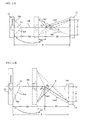
- FIG. 3A is a conceptual diagram of the multiconductor cable in the first embodiment of the present invention
- Fig. 3B is a conceptual diagram of the multiconductor cable in the second embodiment of the present invention.
- the cable width at the end is denoted as D
- the distance between the ends is denoted as E
- the length of one of the transforming portions is denoted as E1
- the length of the other is denoted as E2
- the length of the bundled portion as E3
- the minimum length among the lengths of the wires placed between the ends as Ls
- Lm the maximum length
- the present invention deals with a multiconductor cable that has the distance E less than six times the width D and therefore is considered to be prone to break.
- the wire having the minimum length Ls is placed at the center of the wire array. Therefore, the relation "Ls ⁇ E" is established.
- the wire having the maximum length Lm is placed at the outermost position of the wire array.
- the length Lm is expressed as "Lm1 + Lm2 + E3,” where Lm1 is the length of the bent and slanted portion at one of the transforming portions 12a, Lm2 is the length of the bent and slanted portion at the other, and E3 is the length of the bundled portion.
- the difference between the maximum length Lm and the minimum length Ls, i.e., "Lm - Ls” is equal to "Lm1 + Lm2 - E1 - E2.”
- the wire having the minimum length Ls is placed at one of the outermost positions of the wire array. Therefore, the relation "Ls ⁇ E" is established.
- the wire having the maximum length Lm is placed at the other outermost position of the wire array.
- the length Lm is expressed as "Lm1 + Lm2 + E3,” where Lm1 is the length of the bent and slanted portion at one of the transforming portions 12a, Lm2 is the length of the bent and slanted portion at the other, and E3 is the length of the bundled portion.
- the difference between the maximum length Lm and the minimum length Ls, i.e., "Lm - Ls” is equal to "Lm1 + Lm2 - E1 - E2.”
- the wire that is placed at the outermost position of the array and that has the maximum length Lm be formed to have an angle, ⁇ , of less than 45 degrees, where the angle ⁇ is an angle produced by a wire placed from the end to the bundled intermediate portion and the center axis of the bundled intermediate portion (see Figs. 3A and 3B about the angle ⁇ ).
- the relation "D ⁇ E" can be achieved. Consequently, the relation "Lm - Ls > D(2 1/2 -1) ⁇ 0.41D" can be achieved.
- the relation "2D ⁇ E" can be achieved. Consequently, the relation "Lm - Ls > 2D(2 1/2 -1) ⁇ 0.83D" can be achieved.
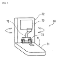
- FIG. 7 is a perspective view illustrating an embodiment of an information device of the present invention.
- a cellular mobile phone 70 has a main body 71 and a display 72, which are connected with each other by a hinge 73.
- the main body 71 houses a main board (not shown), and the display 72 is provided with a liquid crystal panel 75.
- the main board and the liquid crystal panel 75 are linked with each other by a multiconductor cable 76 passing through the portion of the hinge 73.
- a multiconductor cable having the above-described structure is used for the wiring through a turning portion such as the connection between a main board and a liquid crystal display of a cellular mobile phone, a notebook-size computer, a video camera, and the like, it is used at a place where it undergoes twisting with a twisting angle of 90 to 180 degrees (80 to 190 degrees when a margin is considered).
- a twisting angle of 90 to 180 degrees 80 to 190 degrees when a margin is considered.
- the central position may deviate. Consequently, it is difficult to maintain the value of "Lm - Ls" at the calculated value. Therefore, it is necessary to predetermine the value of "Lm - Ls," which is the difference between the maximum length Lm and the minimum length Ls, with a certain margin.
- the embodiment that maximizes the value of "Lm - Ls," which is the difference between the maximum length Lm and the minimum length Ls, is the embodiment under the condition that the bundling is performed by using as the reference the wire that is placed at one of the outermost positions of the wire array and that has the minimum length Ls as explained by referring to Fig. 3B.
- the cable satisfy the following formulae: ⁇ ⁇ 45 degrees, and (Lm - Ls) ⁇ 3 ⁇ ⁇ 2D(2 1/2 -1) ⁇ ⁇ 2.5D, where ⁇ is the angle produced by a wire' portion from one of the ends to the intermediate portion and the same wire' portion in the intermediate portion, Lm is the maximum length, and Ls is the minimum length.
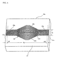
- Figure 4 is a perspective view of an example of an arranging tool for producing a multiconductor cable in the first embodiment of the present invention (this example is for producing one cable at a time).
- Figure 5 is a perspective view of another example of an arranging tool for producing a multiconductor cable in the first embodiment of the present invention (this example is for producing a plurality of cables at a time).
- Figure 4 shows an arranging tool 20a, which is formed as a block having the shape of a rectangular parallelepiped, having a flat arranging face 21.
- the arranging face 21 is provided with a plurality of wire-holding grooves 22 having different lengths.
- the wire-holding grooves 22 have a cross section of a V or U shape. The groove has such a depth that when a wire is held in the groove, the top of the wire is flush with the surface of the arranging face 21 or slightly above it.
- a transforming-portion-arranging section 22a is formed at both sides such that the section has grooves parallel with one another with a pitch according to the wire-arranging pitch at the ends of the multiconductor cable to be produced.
- An intermediate-portion-arranging section 22b is formed in the following way.
- the shortest linear groove at the center has a minimum length of Lsa.
- the outermost grooves have a maximum length of Lma.
- the grooves increase their length successively as their position moves from the center to the outside, so that they are bent with an angular shape or a curved shape.
- a plurality of wires are placed on the arranging face 21 of the arranging tool 20a, and they are squeezed into the wire-holding grooves 22 by using a spatula or a similar tool so that they can be arranged.
- a sticking member for example, an adhesive tape is attached onto at least the transforming-portion-arranging sections 22a at both sides, so that the wires held in the wire-holding grooves 22 are fixed so as to maintain the arranged state.
- the adhesive tape may be made of polyethylene or other plastic on which adhesive is applied.
- both ends of the wires are neatly aligned along an edge 21a of the arranging tool 20a by cutting or another method.
- the wires maintained in the arranged state are removed from the arranging tool 20a.
- An electrical connector or another terminating member is connected to both ends of the wires, as shown in Fig. 1A.
- the intermediate portions of the wires are bundled to form a multiconductor cable, as shown in Fig. 1B.
- the transforming-portion-arranging section 22a of the arranging tool 20a has an arranging width, Da, which is nearly the same as the cable width D shown in Fig. 1A.
- the length at both ends of the wire-holding grooves 22 for connecting the electrical connector or another terminating member is denoted as ⁇ E.
- the wire-holding-groove-forming portion has an effective length, Ea, which is obtained by excluding the length ⁇ E.
- the effective length Ea is predetermined to be the same as the distance E shown in Fig. 1A.
- the wire-holding-groove-forming portion of the arranging tool satisfy the following formulae: Da/Ea > 1/6, and (Lma - Lsa) > ⁇ (Da 2 + Ea 2 ) 1/2 - Ea ⁇ , where Da is the arranging width at the transforming-portion-arranging section, and Ea is the effective length of the wire-holding-groove-forming portion.
- Figure 5 shows an arranging tool 20b in which a plurality of wire-holding-groove-forming portions each for forming one multiconductor cable are connected in tandem.
- This tool can produce a plurality of multiconductor cables concurrently.
- the arranging tool 20b has an arranging face 21 on which the following two members are formed alternately: one is an transforming-portion-arranging section 22a for arranging the transforming portion of a multiconductor cable, and the other is an intermediate-portion-arranging section 22b for arranging the intermediate portion at which the wires are bundled (both members have a structure similar to those formed in the arranging tool 20a).
- This structure enables concurrent wire arranging for a plurality of multiconductor cables.
- FIGS. 4 and 5 show examples of arranging tools for producing the multiconductor cable having the shape shown in Figs. 1A and 1B. Nevertheless, the multiconductor cable having the shape shown in Figs. 2A and 2B can also be produced by using a similar arranging tool with uniform quality and at a low cost.
- the present invention even though a multiconductor cable has a small total length, the intermediate portions of the wires constituting the cable can be bundled together effectively. Therefore, the present invention enables the achievement of a miniaturized multiconductor cable.
Landscapes
- Engineering & Computer Science (AREA)
- Manufacturing & Machinery (AREA)
- Insulated Conductors (AREA)
- Communication Cables (AREA)
Applications Claiming Priority (2)
| Application Number | Priority Date | Filing Date | Title |
|---|---|---|---|
| JP2004046375 | 2004-02-23 | ||
| JP2004046375A JP3843984B2 (ja) | 2004-02-23 | 2004-02-23 | コネクタ付き多心ケーブル |
Publications (2)
| Publication Number | Publication Date |
|---|---|
| EP1566815A2 true EP1566815A2 (de) | 2005-08-24 |
| EP1566815A3 EP1566815A3 (de) | 2006-02-22 |
Family
ID=34709178
Family Applications (1)
| Application Number | Title | Priority Date | Filing Date |
|---|---|---|---|
| EP05250922A Withdrawn EP1566815A3 (de) | 2004-02-23 | 2005-02-17 | Mehrleiterkabel und dessen Herstellungsverfahren. |
Country Status (6)
| Country | Link |
|---|---|
| US (2) | US7098404B2 (de) |
| EP (1) | EP1566815A3 (de) |
| JP (1) | JP3843984B2 (de) |
| KR (2) | KR101028951B1 (de) |
| CN (2) | CN100501878C (de) |
| MY (1) | MY140023A (de) |
Cited By (7)
| Publication number | Priority date | Publication date | Assignee | Title |
|---|---|---|---|---|
| CN102195221A (zh) * | 2010-03-10 | 2011-09-21 | 住友电气工业株式会社 | 细径同轴电缆束及其制造方法 |
| US9048521B2 (en) | 2011-03-24 | 2015-06-02 | Etegent Technologies, Ltd. | Broadband waveguide |
| US9182306B2 (en) | 2011-06-22 | 2015-11-10 | Etegent Technologies, Ltd. | Environmental sensor with tensioned wire exhibiting varying transmission characteristics in response to environmental conditions |
| US10352778B2 (en) | 2013-11-01 | 2019-07-16 | Etegent Technologies, Ltd. | Composite active waveguide temperature sensor for harsh environments |
| US10852277B2 (en) | 2014-04-09 | 2020-12-01 | Etegent Technologies, Ltd. | Active waveguide excitation and compensation |
| US10854941B2 (en) | 2013-11-01 | 2020-12-01 | Etegent Technologies, Ltd. | Broadband waveguide |
| US11473981B2 (en) | 2017-04-10 | 2022-10-18 | Etegent Technologies Ltd. | Damage detection for mechanical waveguide sensor |
Families Citing this family (22)
| Publication number | Priority date | Publication date | Assignee | Title |
|---|---|---|---|---|
| JP4860944B2 (ja) * | 2005-05-25 | 2012-01-25 | 株式会社潤工社 | フラットケーブル |
| JP2007134139A (ja) * | 2005-11-09 | 2007-05-31 | Fujikura Ltd | 極細ケーブルアセンブリ |
| JP4867389B2 (ja) * | 2006-02-22 | 2012-02-01 | 住友電気工業株式会社 | 多心ケーブルの製造方法 |
| JP4910418B2 (ja) * | 2006-02-22 | 2012-04-04 | 住友電気工業株式会社 | 多心ケーブルの製造方法 |
| JP4636002B2 (ja) * | 2006-10-20 | 2011-02-23 | 住友電気工業株式会社 | 多心ケーブルとその製造方法 |
| JP4948140B2 (ja) * | 2006-12-04 | 2012-06-06 | モレックス インコーポレイテド | 不等長多心ケーブル製造方法及び装置 |
| US8063310B2 (en) | 2007-02-05 | 2011-11-22 | Fujikura Ltd. | Electronic device and harness for wiring electronic devices |
| JP4168079B2 (ja) * | 2007-02-05 | 2008-10-22 | 株式会社フジクラ | 電子機器および電子機器におけるハーネスの配線方法 |
| JP5128141B2 (ja) | 2007-02-05 | 2013-01-23 | 株式会社フジクラ | 電子機器及び電子機器配線用ハーネス |
| US7575480B2 (en) * | 2007-03-28 | 2009-08-18 | Adc Dsl Systems, Inc. | Crossbar cable including encasing wrap |
| JP2008257905A (ja) * | 2007-04-02 | 2008-10-23 | Fujikura Ltd | コネクタ付きケーブルアッセンブル |
| JP2008262729A (ja) * | 2007-04-10 | 2008-10-30 | Sumitomo Electric Ind Ltd | ケーブルハーネス |
| JP2008270038A (ja) * | 2007-04-23 | 2008-11-06 | Junkosha Co Ltd | ケーブル |
| TWI412197B (zh) * | 2008-03-06 | 2013-10-11 | Sumitomo Electric Industries | 細徑同軸纜線線束及其連接構造與製造方法 |
| US8772636B2 (en) | 2008-06-25 | 2014-07-08 | Yazaki Corporation | Wire harness installation structure and wire harness-flattening band |
| JP5505069B2 (ja) * | 2009-06-23 | 2014-05-28 | 日立金属株式会社 | ケーブルハーネス |
| KR20120088531A (ko) * | 2009-11-27 | 2012-08-08 | 스미토모 덴키 고교 가부시키가이샤 | 소직경 동축 케이블 하니스 및 그 제조 방법 |
| CN102194545B (zh) * | 2010-03-10 | 2012-09-19 | 住友电气工业株式会社 | 细径同轴电缆束 |
| CN104158006A (zh) * | 2014-08-25 | 2014-11-19 | 苏州胜信光电科技有限公司 | 一种带连接器扁平电缆及其裁剪模具 |
| US10460853B2 (en) | 2016-05-24 | 2019-10-29 | Flex-Cable | Power cable and bus bar with transitional cross sections |
| CN110012594A (zh) * | 2019-04-19 | 2019-07-12 | 维沃移动通信有限公司 | 一种柔性电路板及终端设备 |
| US20230023483A1 (en) * | 2022-09-27 | 2023-01-26 | Intel Corporation | Methods and apparatus to enable customization of pigtail lengths of optical connectors |
Citations (2)
| Publication number | Priority date | Publication date | Assignee | Title |
|---|---|---|---|---|
| JPS6139817U (ja) * | 1984-08-16 | 1986-03-13 | 岡野電線株式会社 | 多心ケ−ブル |
| JP2000294045A (ja) * | 1999-04-07 | 2000-10-20 | Japan Aviation Electronics Industry Ltd | フラットリボンケーブル |
Family Cites Families (19)
| Publication number | Priority date | Publication date | Assignee | Title |
|---|---|---|---|---|
| CH280298A (de) * | 1948-11-17 | 1952-01-15 | Sprecher & Schuh Ag | Isolierter Mehrfachleiter. |
| FR1544150A (fr) * | 1967-09-20 | 1968-10-31 | Prec Mecanique Labinal | Perfectionnements apportés aux procédés d'assemblage de conducteurs électriques |
| FR2111979A1 (de) * | 1970-10-31 | 1972-06-09 | Rists Wires & Cables Ltd | |
| US3881976A (en) * | 1973-02-16 | 1975-05-06 | American Optical Corp | Fiber bundles for ornamental display devices and method of making same |
| FR2266430A1 (en) * | 1974-03-29 | 1975-10-24 | Rists Wires & Cables Ltd | Make-up jig for automobile cable harness - has weld current paths between electrode contact points |
| JPS6023858Y2 (ja) | 1980-05-16 | 1985-07-16 | 日立電線株式会社 | フラツトケ−ブルの製造装置 |
| JPS607109U (ja) * | 1983-06-27 | 1985-01-18 | 三菱電機株式会社 | チユ−ブ収納形フラツトケ−ブル |
| JPS60181815U (ja) | 1984-05-14 | 1985-12-03 | 日立電線株式会社 | フラツトケ−ブル |
| JPS61230208A (ja) * | 1985-04-05 | 1986-10-14 | 株式会社フジクラ | スダレ形多心ケ−ブル |
| JPS62271309A (ja) * | 1986-05-19 | 1987-11-25 | タツタ電線株式会社 | 電線端を平形に成端する方法 |
| US4723055A (en) * | 1987-03-17 | 1988-02-02 | Dresser Industries, Inc. | Multi-wire conduit dam and method of forming same |
| US4874908A (en) * | 1987-07-08 | 1989-10-17 | Minnesota Mining And Manufacturing Company | Wiring harness |
| JP2900342B2 (ja) * | 1988-12-27 | 1999-06-02 | 矢崎総業株式会社 | フラットワイヤハーネスの製造方法および装置 |
| JP3144445B2 (ja) * | 1993-01-29 | 2001-03-12 | 矢崎総業株式会社 | フラットワイヤハーネスの製造方法および取付具を備えたフラットワイヤハーネス |
| JP3602208B2 (ja) * | 1995-07-20 | 2004-12-15 | 矢崎総業株式会社 | ワイヤーハーネスおよびその製造方法 |
| US5669775A (en) * | 1995-09-05 | 1997-09-23 | International Business Machines Corporation | Assembly for mounting components to flexible cables |
| JPH09282946A (ja) * | 1996-04-18 | 1997-10-31 | Harness Sogo Gijutsu Kenkyusho:Kk | ワイヤーハーネス及びその製造方法 |
| US6230404B1 (en) * | 1996-05-09 | 2001-05-15 | Sumitomo Wiring Systems, Ltd. | Method and apparatus for producing a wiring harness |
| JP2002209323A (ja) * | 2001-01-09 | 2002-07-26 | Sumitomo Wiring Syst Ltd | ワイヤハーネスの防水処理方法及び装置 |
-
2004
- 2004-02-23 JP JP2004046375A patent/JP3843984B2/ja not_active Expired - Lifetime
-
2005
- 2005-02-16 US US11/058,415 patent/US7098404B2/en not_active Expired - Lifetime
- 2005-02-17 EP EP05250922A patent/EP1566815A3/de not_active Withdrawn
- 2005-02-17 KR KR1020050013122A patent/KR101028951B1/ko not_active Expired - Fee Related
- 2005-02-18 CN CNB2005100519029A patent/CN100501878C/zh not_active Expired - Lifetime
- 2005-02-18 CN CNA2008101694353A patent/CN101414494A/zh active Pending
- 2005-02-21 MY MYPI20050654A patent/MY140023A/en unknown
-
2006
- 2006-08-03 US US11/498,133 patent/US7406763B2/en not_active Expired - Lifetime
-
2011
- 2011-02-17 KR KR1020110014224A patent/KR101109835B1/ko not_active Expired - Fee Related
Patent Citations (2)
| Publication number | Priority date | Publication date | Assignee | Title |
|---|---|---|---|---|
| JPS6139817U (ja) * | 1984-08-16 | 1986-03-13 | 岡野電線株式会社 | 多心ケ−ブル |
| JP2000294045A (ja) * | 1999-04-07 | 2000-10-20 | Japan Aviation Electronics Industry Ltd | フラットリボンケーブル |
Cited By (11)
| Publication number | Priority date | Publication date | Assignee | Title |
|---|---|---|---|---|
| CN102195221A (zh) * | 2010-03-10 | 2011-09-21 | 住友电气工业株式会社 | 细径同轴电缆束及其制造方法 |
| CN102195221B (zh) * | 2010-03-10 | 2014-12-03 | 住友电气工业株式会社 | 细径同轴电缆束及其制造方法 |
| US9048521B2 (en) | 2011-03-24 | 2015-06-02 | Etegent Technologies, Ltd. | Broadband waveguide |
| WO2012129478A3 (en) * | 2011-03-24 | 2016-03-24 | Etegent Technologies Ltd. | Broadband waveguide |
| US9182306B2 (en) | 2011-06-22 | 2015-11-10 | Etegent Technologies, Ltd. | Environmental sensor with tensioned wire exhibiting varying transmission characteristics in response to environmental conditions |
| US10352778B2 (en) | 2013-11-01 | 2019-07-16 | Etegent Technologies, Ltd. | Composite active waveguide temperature sensor for harsh environments |
| US10854941B2 (en) | 2013-11-01 | 2020-12-01 | Etegent Technologies, Ltd. | Broadband waveguide |
| US10852277B2 (en) | 2014-04-09 | 2020-12-01 | Etegent Technologies, Ltd. | Active waveguide excitation and compensation |
| US11982648B2 (en) | 2014-04-09 | 2024-05-14 | Etegent Technologies, Ltd. | Active waveguide excitation and compensation |
| US11473981B2 (en) | 2017-04-10 | 2022-10-18 | Etegent Technologies Ltd. | Damage detection for mechanical waveguide sensor |
| US11686627B2 (en) | 2017-04-10 | 2023-06-27 | Etegent Technologies Ltd. | Distributed active mechanical waveguide sensor driven at multiple frequencies and including frequency-dependent reflectors |
Also Published As
| Publication number | Publication date |
|---|---|
| KR20060042046A (ko) | 2006-05-12 |
| CN100501878C (zh) | 2009-06-17 |
| KR101028951B1 (ko) | 2011-04-12 |
| MY140023A (en) | 2009-11-30 |
| KR101109835B1 (ko) | 2012-02-13 |
| US7406763B2 (en) | 2008-08-05 |
| CN1661730A (zh) | 2005-08-31 |
| EP1566815A3 (de) | 2006-02-22 |
| US20050183881A1 (en) | 2005-08-25 |
| US20060266541A1 (en) | 2006-11-30 |
| CN101414494A (zh) | 2009-04-22 |
| JP3843984B2 (ja) | 2006-11-08 |
| US7098404B2 (en) | 2006-08-29 |
| KR20110023874A (ko) | 2011-03-08 |
| JP2005235690A (ja) | 2005-09-02 |
Similar Documents
| Publication | Publication Date | Title |
|---|---|---|
| US7098404B2 (en) | Multiconductor cable and method of producing the cable | |
| KR101001804B1 (ko) | 동축케이블 접속구조, 그것에 이용되는 동축케이블 하네스, 및 휴대단말기기 | |
| CN101286378B (zh) | 电缆束 | |
| EP1953768A2 (de) | Elektronische Vorrichtung und Kabelbaum zum Verdrahten einer elektronischen Vorrichtung | |
| CN102227856B (zh) | 细径同轴电缆束及其制造方法 | |
| US5147510A (en) | Flat multicore wire and method of forming the same wire | |
| CN101026026B (zh) | 多共轴线缆及其制造方法 | |
| JP4661428B2 (ja) | 同軸ケーブル接続構造 | |
| JP2013026181A (ja) | 細径ケーブルハーネス | |
| JP5463953B2 (ja) | 細径同軸ケーブルハーネス及びその製造方法 | |
| US9318816B2 (en) | Electric connector and terminal included in the same | |
| JP4834959B2 (ja) | 配線部材及びその製造方法 | |
| JP4910504B2 (ja) | 多心ケーブルの製造方法 | |
| JP7516142B2 (ja) | 複合ケーブル、複合ケーブル用の電源ケーブル、ワイヤハーネス及び複合ケーブルの製造方法 | |
| KR200466631Y1 (ko) | 소경 동축 케이블 하네스 | |
| JP4910418B2 (ja) | 多心ケーブルの製造方法 | |
| JP2011060466A (ja) | 細径同軸電線ハーネス及び基板付き細径同軸電線ハーネス | |
| JP5229198B2 (ja) | 細径同軸ケーブルハーネス及びその製造方法 | |
| JP4636002B2 (ja) | 多心ケーブルとその製造方法 | |
| KR101171665B1 (ko) | 소직경 동축 케이블 하니스, 및 기판이 붙어 있는 소직경 동축 케이블 하니스 | |
| EP1244177A1 (de) | Verbindungsvorrichtung und Verfahren um daran eines Kabel zu verbinden | |
| JP2000195341A (ja) | フラットケ―ブル | |
| TW201225757A (en) | Small diameter coaxial cable harness and small diameter coaxial cable harness with substrate | |
| JP2009117197A (ja) | ケーブルアセンブリ |
Legal Events
| Date | Code | Title | Description |
|---|---|---|---|
| PUAI | Public reference made under article 153(3) epc to a published international application that has entered the european phase |
Free format text: ORIGINAL CODE: 0009012 |
|
| AK | Designated contracting states |
Kind code of ref document: A2 Designated state(s): AT BE BG CH CY CZ DE DK EE ES FI FR GB GR HU IE IS IT LI LT LU MC NL PL PT RO SE SI SK TR |
|
| AX | Request for extension of the european patent |
Extension state: AL BA HR LV MK YU |
|
| PUAL | Search report despatched |
Free format text: ORIGINAL CODE: 0009013 |
|
| AK | Designated contracting states |
Kind code of ref document: A3 Designated state(s): AT BE BG CH CY CZ DE DK EE ES FI FR GB GR HU IE IS IT LI LT LU MC NL PL PT RO SE SI SK TR |
|
| AX | Request for extension of the european patent |
Extension state: AL BA HR LV MK YU |
|
| 17P | Request for examination filed |
Effective date: 20060420 |
|
| AKX | Designation fees paid |
Designated state(s): AT BE BG CH CY CZ DE DK EE ES FI FR GB GR HU IE IS IT LI LT LU MC NL PL PT RO SE SI SK TR |
|
| 17Q | First examination report despatched |
Effective date: 20130325 |
|
| STAA | Information on the status of an ep patent application or granted ep patent |
Free format text: STATUS: THE APPLICATION IS DEEMED TO BE WITHDRAWN |
|
| 18D | Application deemed to be withdrawn |
Effective date: 20140114 |