EP1560085B1 - Resolver/Digital-Wandler und Steuergerät mit Hilfe eines solchen Wandlers - Google Patents
Resolver/Digital-Wandler und Steuergerät mit Hilfe eines solchen Wandlers Download PDFInfo
- Publication number
- EP1560085B1 EP1560085B1 EP05001744A EP05001744A EP1560085B1 EP 1560085 B1 EP1560085 B1 EP 1560085B1 EP 05001744 A EP05001744 A EP 05001744A EP 05001744 A EP05001744 A EP 05001744A EP 1560085 B1 EP1560085 B1 EP 1560085B1
- Authority
- EP
- European Patent Office
- Prior art keywords
- resolver
- signals
- digital
- failure
- signal
- Prior art date
- Legal status (The legal status is an assumption and is not a legal conclusion. Google has not performed a legal analysis and makes no representation as to the accuracy of the status listed.)
- Expired - Lifetime
Links
- 238000006243 chemical reaction Methods 0.000 claims description 30
- 230000007246 mechanism Effects 0.000 claims description 8
- 238000001514 detection method Methods 0.000 claims description 6
- 230000008859 change Effects 0.000 claims description 4
- 230000001934 delay Effects 0.000 claims 1
- 230000006870 function Effects 0.000 description 61
- 238000010586 diagram Methods 0.000 description 39
- 230000016507 interphase Effects 0.000 description 37
- 238000003745 diagnosis Methods 0.000 description 26
- 238000000034 method Methods 0.000 description 23
- 230000005856 abnormality Effects 0.000 description 11
- 239000004065 semiconductor Substances 0.000 description 8
- 239000003990 capacitor Substances 0.000 description 5
- 230000002159 abnormal effect Effects 0.000 description 4
- 230000000694 effects Effects 0.000 description 4
- 230000008569 process Effects 0.000 description 4
- 230000014509 gene expression Effects 0.000 description 3
- 230000003111 delayed effect Effects 0.000 description 2
- 238000012544 monitoring process Methods 0.000 description 2
- 238000004804 winding Methods 0.000 description 2
- 230000009471 action Effects 0.000 description 1
- 230000007547 defect Effects 0.000 description 1
- 230000002950 deficient Effects 0.000 description 1
- 230000009977 dual effect Effects 0.000 description 1
- 238000011084 recovery Methods 0.000 description 1
- 230000009467 reduction Effects 0.000 description 1
- 230000009897 systematic effect Effects 0.000 description 1
- 230000001052 transient effect Effects 0.000 description 1
Images


Classifications
-
- B—PERFORMING OPERATIONS; TRANSPORTING
- B60—VEHICLES IN GENERAL
- B60T—VEHICLE BRAKE CONTROL SYSTEMS OR PARTS THEREOF; BRAKE CONTROL SYSTEMS OR PARTS THEREOF, IN GENERAL; ARRANGEMENT OF BRAKING ELEMENTS ON VEHICLES IN GENERAL; PORTABLE DEVICES FOR PREVENTING UNWANTED MOVEMENT OF VEHICLES; VEHICLE MODIFICATIONS TO FACILITATE COOLING OF BRAKES
- B60T8/00—Arrangements for adjusting wheel-braking force to meet varying vehicular or ground-surface conditions, e.g. limiting or varying distribution of braking force
- B60T8/32—Arrangements for adjusting wheel-braking force to meet varying vehicular or ground-surface conditions, e.g. limiting or varying distribution of braking force responsive to a speed condition, e.g. acceleration or deceleration
- B60T8/88—Arrangements for adjusting wheel-braking force to meet varying vehicular or ground-surface conditions, e.g. limiting or varying distribution of braking force responsive to a speed condition, e.g. acceleration or deceleration with failure responsive means, i.e. means for detecting and indicating faulty operation of the speed responsive control means
- B60T8/885—Arrangements for adjusting wheel-braking force to meet varying vehicular or ground-surface conditions, e.g. limiting or varying distribution of braking force responsive to a speed condition, e.g. acceleration or deceleration with failure responsive means, i.e. means for detecting and indicating faulty operation of the speed responsive control means using electrical circuitry
-
- B—PERFORMING OPERATIONS; TRANSPORTING
- B62—LAND VEHICLES FOR TRAVELLING OTHERWISE THAN ON RAILS
- B62D—MOTOR VEHICLES; TRAILERS
- B62D5/00—Power-assisted or power-driven steering
- B62D5/04—Power-assisted or power-driven steering electrical, e.g. using an electric servo-motor connected to, or forming part of, the steering gear
- B62D5/0457—Power-assisted or power-driven steering electrical, e.g. using an electric servo-motor connected to, or forming part of, the steering gear characterised by control features of the drive means as such
- B62D5/0481—Power-assisted or power-driven steering electrical, e.g. using an electric servo-motor connected to, or forming part of, the steering gear characterised by control features of the drive means as such monitoring the steering system, e.g. failures
-
- G—PHYSICS
- G01—MEASURING; TESTING
- G01D—MEASURING NOT SPECIALLY ADAPTED FOR A SPECIFIC VARIABLE; ARRANGEMENTS FOR MEASURING TWO OR MORE VARIABLES NOT COVERED IN A SINGLE OTHER SUBCLASS; TARIFF METERING APPARATUS; MEASURING OR TESTING NOT OTHERWISE PROVIDED FOR
- G01D5/00—Mechanical means for transferring the output of a sensing member; Means for converting the output of a sensing member to another variable where the form or nature of the sensing member does not constrain the means for converting; Transducers not specially adapted for a specific variable
- G01D5/12—Mechanical means for transferring the output of a sensing member; Means for converting the output of a sensing member to another variable where the form or nature of the sensing member does not constrain the means for converting; Transducers not specially adapted for a specific variable using electric or magnetic means
- G01D5/14—Mechanical means for transferring the output of a sensing member; Means for converting the output of a sensing member to another variable where the form or nature of the sensing member does not constrain the means for converting; Transducers not specially adapted for a specific variable using electric or magnetic means influencing the magnitude of a current or voltage
- G01D5/20—Mechanical means for transferring the output of a sensing member; Means for converting the output of a sensing member to another variable where the form or nature of the sensing member does not constrain the means for converting; Transducers not specially adapted for a specific variable using electric or magnetic means influencing the magnitude of a current or voltage by varying inductance, e.g. by a movable armature
- G01D5/204—Mechanical means for transferring the output of a sensing member; Means for converting the output of a sensing member to another variable where the form or nature of the sensing member does not constrain the means for converting; Transducers not specially adapted for a specific variable using electric or magnetic means influencing the magnitude of a current or voltage by varying inductance, e.g. by a movable armature by influencing the mutual induction between two or more coils
- G01D5/2073—Mechanical means for transferring the output of a sensing member; Means for converting the output of a sensing member to another variable where the form or nature of the sensing member does not constrain the means for converting; Transducers not specially adapted for a specific variable using electric or magnetic means influencing the magnitude of a current or voltage by varying inductance, e.g. by a movable armature by influencing the mutual induction between two or more coils by movement of a single coil with respect to two or more coils
-
- G—PHYSICS
- G05—CONTROLLING; REGULATING
- G05B—CONTROL OR REGULATING SYSTEMS IN GENERAL; FUNCTIONAL ELEMENTS OF SUCH SYSTEMS; MONITORING OR TESTING ARRANGEMENTS FOR SUCH SYSTEMS OR ELEMENTS
- G05B9/00—Safety arrangements
- G05B9/02—Safety arrangements electric
-
- H—ELECTRICITY
- H03—ELECTRONIC CIRCUITRY
- H03M—CODING; DECODING; CODE CONVERSION IN GENERAL
- H03M1/00—Analogue/digital conversion; Digital/analogue conversion
- H03M1/10—Calibration or testing
- H03M1/1071—Measuring or testing
- H03M1/1076—Detection or location of converter hardware failure, e.g. power supply failure, open or short circuit
-
- B—PERFORMING OPERATIONS; TRANSPORTING
- B60—VEHICLES IN GENERAL
- B60T—VEHICLE BRAKE CONTROL SYSTEMS OR PARTS THEREOF; BRAKE CONTROL SYSTEMS OR PARTS THEREOF, IN GENERAL; ARRANGEMENT OF BRAKING ELEMENTS ON VEHICLES IN GENERAL; PORTABLE DEVICES FOR PREVENTING UNWANTED MOVEMENT OF VEHICLES; VEHICLE MODIFICATIONS TO FACILITATE COOLING OF BRAKES
- B60T2270/00—Further aspects of brake control systems not otherwise provided for
- B60T2270/40—Failsafe aspects of brake control systems
- B60T2270/402—Back-up
-
- H—ELECTRICITY
- H03—ELECTRONIC CIRCUITRY
- H03M—CODING; DECODING; CODE CONVERSION IN GENERAL
- H03M1/00—Analogue/digital conversion; Digital/analogue conversion
- H03M1/12—Analogue/digital converters
- H03M1/64—Analogue/digital converters with intermediate conversion to phase of sinusoidal or similar periodical signals
- H03M1/645—Analogue/digital converters with intermediate conversion to phase of sinusoidal or similar periodical signals for position encoding, e.g. using resolvers or synchros
Definitions
- the present invention relates to a resolver/digital converter, and particularly to a resolver/digital converter having a failure detecting function or to the failure detecting function of the resolver/digital converter.
- the servo control system needs a rotation-angle sensor in order to detect the rotation angle and make the feedback control.
- the brushless motor control also requires the rotation-angle sensor in order to cause current to flow in the coil of the motor in accordance with the rotation angle of the motor as well as the servo control system does.
- the resolver has so far been widely used as a rotation-angle sensor since it is rigid and resistant to the environment because of its simple structure.
- the servo control system that is used for motor-driven power steering, or x-by-wire control system, particularly steer-by-wire or fly-by-wire control system is required to have a failure detecting function because it needs safety and reliability.
- a resolver/digital converter has been developed for converting the signal from the resolver to a rotation angle and supplying it as digital data to a microcomputer or the like (see the catalog of Smartcoder AU6802, Tamagawa Seiki Co., T12-159N1 (Apr. 20, 2002), http://www.tamagawaseiki.co.jp/ct1/1591n3j.pdf (nonpatent literature 1)).
- the resolver/digital converter forms a feedback loop that the estimate ⁇ of a rotation angle is modified by the residual error ⁇ resulting from the computation of sin( ⁇ ), cos( ⁇ ) generated from the estimate ⁇ of rotation angle and the input signal, thereby making the estimate ⁇ of rotation angle be converged to the actual rotation angle ⁇ .
- This system also has the function to notify the microcomputer of the occurrence of a failure when the residual error ⁇ exceeds a certain value.
- an abnormality-detecting signal processor for finding the angle ⁇ is provided independently of an angle-detecting signal processor, and the failure is detected from the difference between the angles ⁇ produced from both processors.
- US 5347277 shows a dual phase resolver to digital converter having two separate channels for generating rotor position data. The data from the two channels are selectively combined in the output of the converter in order to provide greater accuracy.
- the signal from or to the resolver if the signal from or to the resolver is disconnected, the signal from the resolver becomes abnormal, and thus it does not satisfy the relation between sin( ⁇ ) and cos( ⁇ ) that is the condition of the feedback loop convergence. As a result, the residual error ⁇ becomes large, thus this fact being sent to the microcomputer as a failure. Also, if the feedback loop for finding the estimate ⁇ of rotation angle does not work, the residual error ⁇ does not converge, but diverges, thus this fact being sent to the microcomputer as a failure.
- the signal from or to the resolver if the signal from or to the resolver is disconnected, the signal from the resolver becomes abnormal, and thus it does not satisfy the relation between sin ( ⁇ ) and cos ( ⁇ ).
- the value of sin 2 ( ⁇ ) + cos 2 ( ⁇ ) is deviated from 1, a failure is detected, and hence the microcomputer can be informed of the failure.
- the failure that can be detected in this system is only the failure of the abnormal signal waveform due to the disconnection of the signal from or to the resolver. That is, if a failure occurs in the resolver/digital converter function itself that performs the process for finding the angle ⁇ , this failure cannot be detected.
- the computation load is large in finding ⁇ from values of trigonometric functions (sin, cos), and judgment to be made over the boundary between the regions of ⁇ is required to reconsider. For example, when one ⁇ is 1°, the other 359°, the difference between both angles must be judged to be 2°.
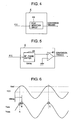
- FIG. 1 is a block diagram of a basic embodiment of a controller 100 having a failure detecting function for detecting the failure in the resolver circuits.
- An exciting current f(t) generated from an exciting signal generator 3 is supplied to a resolver 5.
- the resolver 5 produces resolver signals Y sin and Y cos .
- a resolver/digital converting portion 2 produces an estimated angle ⁇ on the basis of the resolver signals Y sin and Y cos
- the resolver/digital converting-portion 2 also produces an error detection signal and supplies it together with the estimated angle ⁇ to a microcomputer 1.
- the resolver/digital converting portion 2 can be constructed differently, and the typical one can be considered to use the method proposed in the nonpatent document 1.
- the resolver/digital converting portion 2 described in the nonpatent document 1 is the unitary body formed of the resolver/digital converting portion 2 and exciting signal generator 3 built in the same chip.
- an embodiment of the invention further uses a conversion trigger generator 4 to generate a conversion trigger on the basis of the exciting signal f(t), an A/D converter 11 to convert the resolver signals Y sin and Y cos to digital signals by using the conversion trigger, and an error detecting function 12 to detect error due to a failure.
- the conversion trigger generator 4 can also be constructed differently.
- FIG. 2 shows an example of the conversion trigger generator 4 in which a voltage comparator 41 is used to compare the exciting signal f(t) and a reference voltage (V ref ) 42.
- sin( ⁇ ), cos( ⁇ ) and tan( ⁇ ) can be found in the same way as those in the example of FIG. 2 .
- the delay circuit 43 for delaying by t delay can be constructed by a timer provided within the microprocessor, and thus the number of discrete components to be used can be greatly reduced.
- Fig. 4 shows another example of the conversion trigger generator 4 as a peak detector 44.
- the peak detector 44 can be achieved by a method for differentiating the exciting signal f(t) and finding the time when it becomes zero, a method for using a phase shifter to delay the exciting signal f(t) by 90 degrees so that the zero cross can be obtained, or a method for holding peaks in turn while they are being updated, and finding as a time of peak the time when the current value becomes below the held peak value.
- the values of sin ( ⁇ ), cos ( ⁇ ) and tan ( ⁇ ) are found in the same way as those in the embodiments shown in FIGS. 2 and 3 . If the differences of those values to the values of sin ( ⁇ ), cos ( ⁇ ) and tan ( ⁇ ) are within the allowable ranges, the result is regarded as normal. If the differences are out of the allowable ranges, the result can be judged to be a failure.
- FIG. 5 is still another detailed embodiment in which a phase shifter 45 is used to delay the phase of the exciting signal f(t) by 90 degrees and the comparator 41 is used to take zero cross points.
- the exciting signal f(t) is fed to the 90°-phase shifter 45 so that it is delayed in phase by 90 degrees.
- the delayed signal is compared to a reference value by the comparator 41 so that the zero cross point can be detected.
- the output from the comparator 41 is used as the conversion trigger. If the 90°-phase shifter 45 is formed of primary delay elements of a resistor and a capacitor, it is able to delay the phase of the exciting signal by about 90 degrees over a range from the cutoff frequency to a sufficiently high frequency.
- FIG. 6 is a waveform diagram showing the conversion timings for the resolver signals Y sin and Y cos in each embodiment shown in FIGS. 2 through 4 .
- the abscissa is time, and the ordinate is the amplitudes of the resolver signals Y sin and Y cos , and the exciting signal f(t).
- the resolver signals Y sin and Y cos are converted at the time when the exciting signal f(t) reaches V ref , or at point A.
- the resolver signals are converted at the time when the exciting signal f(t) has progressed t delay from the zero cross point, or at time B.
- the resolver signals Y sin and Y cos are converted when the exciting signal f(t) reaches the peak.
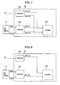
- FIGS. 7 through 9 show embodiments of an abnormality detecting function 12 that detects from those obtained signals Y sin , Y cos the failure occurring in the resolver and resolver/digital converting portion.
- FIG. 7 shows a first embodiment of the abnormality detecting function 12.
- a computing portion 122 finds sin( ⁇ ) and cos( ⁇ ) according to the following expressions.
- sin ⁇ Y sin / SQRT ⁇ Y sin 2 + Y cos 2 ⁇ V ref
- cos ⁇ Y cos / SQRT ⁇ Y sin 2 + Y cos 2 ⁇ V ref
- a computing portion 121 finds sin ( ⁇ ) and cos ⁇ on the basis of the estimated angle ⁇ .
- a comparing function 123 compares the values of sin( ⁇ ) and cos( ⁇ ) with the values of sin( ⁇ ) and cos ( ⁇ ). If the differences are within the allowable ranges, the result is regarded as normal. If the differences are out of the allowable ranges, the result can be judged to be a failure. The failure of the resolver/digital converting portion can be detected by this method.
- FIG. 8 shows another embodiment of the abnormality detecting function 12.
- a computing portion 125 finds tan ( ⁇ ) on the basis of the estimated angle ⁇ .
- the comparing function 123 compares the tan( ⁇ )and the tan ( ⁇ ). If the difference is within the allowable range, the result is regarded as normal. If the difference is out of the range, the result can be judged to be a failure. The failure of the resolver/digital converting portion can be detected by this method.
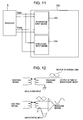
- FIG. 9 is still another embodiment of the abnormality detecting function 12.
- the computing portion 122 finds sin( ⁇ ) and cos ( ⁇ ), and the computing portion 124 finds tan ( ⁇ ).
- Computing portions 126 through 128 respectively find ⁇ 1 , ⁇ 2 and ⁇ 3 by substituting the obtained values of sin ( ⁇ ), cos ( ⁇ ) and tan ( ⁇ ) into the following expressions.
- the comparing function 123 compares the obtained values of ⁇ 1 , ⁇ 2 and ⁇ 3 with each other. If the differences are within the allowable ranges, the result is regarded as normal. If the differences are out of the ranges, the result can be judged to be a failure.
- This method is able to check the reasonableness of the signal from the resolver and detect the failure of the resolver itself.
- FIG. 10 shows an embodiment of the controller 100 that has both normal mode input means 101 that supplies the normal components of resolver signals Y sin and Y cos to the next stage, and common mode input means 102 that supplies the common mode components of the resolver signals to the next stage.
- FIG. 11 shows another embodiment of the controller 100 that has both differential input means 103 that supplies the resolver signals Y sin and Y cos as differential signals to the next stage and single-end input means 104 that supplies the resolver signals as single end signals to the next stage.
- the normal resolver signals cannot be obtained when a single-end configuration is used as shown in FIG. 12 .
- the resolver signals are as indicated by the solid line because they are affected by the inter-phase short circuit.
- the component affected by the inter-phase short circuit is superimposed as a common mode component upon the original signal (normal mode component: broken line) to produce the waveform indicated by the solid line.
- the original resolver signals solid line
- the resolver signals Y sin and Y cos are received by differential-configuration input means, the inter-phase short circuit effect can be avoided.
- the occurrence of the inter-phase short circuit cannot be detected under this condition.
- the common mode input means 102 or single end input means 104 is provided as in the examples of FIGS. 10 and 11 to detect the common mode component that is to be superimposed due to the inter-phase short circuit, a control system can be realized that is not affected by the inter-phase short circuit and that can detect the inter-phase short.
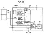
- FIG. 13 shows a specific example of FIGS. 10 and 11 .
- the resolver signals Y sin and Y cos produced from the resolver 5 are supplied through the normal mode input means 101 or differential input means 103 to the resolver/digital converting portion 2, and also fed through the common mode input means 102 or single end input means 104 to the A/D converter 11. Even if an inter-phase short circuit occurs, the resolver/digital converting portion 2 is not affected by the inter-phase short circuit, but can produce the estimated angle ⁇ on the basis of the resolver signals Y sin and Y cos . On the other hand, the input signals to the A/D converter 11 are affected by the inter-phase short circuit. If the error detecting function 12 monitors the input to the A/D converter 11, the inter-phase short circuit occurrence can be detected.
- the signal waveform of the signals supplied to the resolver/digital converting portion 2 that is not affected by the inter-phase short circuit is different from that fed to the A/D converter 11 that is affected by the inter-phase short circuit, and thus the inter-phase short circuit can be detected from the difference between the values of the trigonometric functions based on the signal waveforms or the estimated angles.
- the detection method in the error detecting function 12 may be the method shown in FIGS. 7 through 9 .
- the resolver signals Y sin and Y cos can be supplied through the common mode input means 102 or single end input means 104 to the resolver/digital converting portion 2, and also fed through the normal mode input means 101 or differential input means 103 to the A/D converter 11 of microcomputer, in which case the same effect can also be obtained.
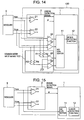
- FIG. 14 shows a more specific example of FIGS. 10 and 13 .
- the solver signals Y sin and Y cos are supplied to the resolver/digital converting portion 2 and to the A/D converter 11 of the microcomputer 1, and the common mode input means 102 is also provided.
- the exciting signal generator 3, resolver 5 and conversion trigger generator 4 are not shown for the sake of simplicity.
- the resolver/digital converting portion 2 also serves as the normal mode input means 101 that supplies the normal mode signals to the next stage or as the differential input means 103 that supplies the differential signals to the next stage.
- the resolver/digital converting portion 2 has, provided at the first stage, differential amplifiers 21 and 22 through which the resolver signals Y sin and Y cos can be received as differential signals.
- Differential amplifiers 51 and 52 are also provided before the A/D converter 11 of the microcomputer 1 in order to receive the resolver signals Y sin and Y cos as differential signals.
- resistors R 1 , R 2 and resistors R 3 , R 4 that constitute the common mode input means 102 can be used to add the common mode components of the resolver signals Y sin and Y cos .
- operational amplifiers 61, 62 produce common mode components of resolver signals Y sin and Y cos with the normal mode components cancelled out.
- FIG. 15 shows another specific example of FIGS. 11 and 13 .
- the resolver signals Y sin and Y cos are supplied as differential signals to the resolver/digital converter portion 2, and fed as single-end signals to the A/D converting portion 11 of microcomputer 1, the resolver/digital converting portion 2 is not affected by the inter-phase short circuit, but the signals affected by the inter-phase short circuit are fed to the A/D converter 11 of microcomputer 1.
- the resolver/digital converting portion 2 also serves as the differential input means 103 of FIG. 21
- the A/D converter 11 of microcomputer 1 also serves as the single-end input means 104.
- the inter-phase short circuit occurrence can be detected from the abnormality of signal waveforms by use of the common mode input means 102 or single end input means 104.
- the electric noise often comes as common mode components
- use of single-end input means 104 for one input side as in the example of FIG. 13 results in the reduction of noise resistance so that the redundancy effect of the input circuits 103, 104 is reduced.
- FIGS. 16 through 25 examples for detecting the inter-phase short circuit occurrence with the noise resistance kept are shown in FIGS. 16 through 25 .
- FIG. 16 shows an embodiment of the invention in which a single-end/differential input means 105 and the differential input means 103 are provided that are supplied with the resolver signals Y sin and Y cos .
- This single-end/differential input means 105 switches the single end input means and differential input means and receives the resolver signals through the selected input means.
- the single-end/differential input means 105 is used instead of the single end input means 104 in order to normally supply the redundant differential input signals to the next stage, and when a diagnosis is made in booting the system just after the power supply is turned on, to supply the single end signals to the next stage so that the inter-phase short circuit can be detected.
- FIG. 17 shows a specific example of the single-end/differential input means 105.
- the single-end/differential input means 105 has an operational amplifier OpAmp, a switch SW, and resistors.
- the output Vo of the operational amplifier OpAmp is supplied to and converted by the A/D converter 11 not shown to digital data.
- the controller 100 it is desired to incorporate the A/D converter 11 in the microcomputer 1 not shown, but it may be discrete as long as the function can be kept.
- the switch SW is desired to control by the microcomputer 1, but it is not always necessary to do so.
- the signal Ysin or Ycos from the resolver is differentially supplied as an input voltage V inp , V inn in this circuit, or each signal Y sin or Y cos is fed to each of two circuits that constitute the single-end/differential input means 105.
- V o R f / R i ⁇ V inp - V inn + V b ⁇ 1 is satisfied.
- V o R f / R i ⁇ V b ⁇ 1 - V inn + V b ⁇ 1 is satisfied.
- the single-end/differential input means operates as the differential input means, and when the switch SW is closed, it operates as the single end input means.
- the differential input means and single-end input means can be switched by opening and closing the switch SW.
- the input means can be constructed as the single-end/differential input means 105.
- the input means can be operated as a differential input means in the normal mode, and operated as a single-end input means in the mode in which the system makes a diagnosis while it is being booted immediately after the power supply is turned on, so that the inter-phase short circuit can be detected.
- FIG. 18 shows an embodiment in which the differential input means 103 is provided to receive the resolver signals Y sin , Y cos and supply differential input signals to the next stage, and frequency division input means 106 is provided to receive the resolver signals and supply the single-end input and differential input signals in a frequency division manner to the next stage.
- the differential input means that is resistant to noise is used for the frequency region including noise components
- the single-end input means is used for the frequency band that is little affected by noise components but much affected by the inter-phase short circuit, so that both inter-phase short detecting function and noise resistance can be made compatible.
- the frequency division input means 106 can be realized by inserting filters (high-pass filter, low-pass filter, band-pass filter and band-stop filter) having pass characteristics depending upon frequency in one of the two input lines of the differential input circuit, or inserting filters having different pass characteristics depending upon frequency in the two input lines.
- filters high-pass filter, low-pass filter, band-pass filter and band-stop filter
- FIGS. 19 through 25 show detailed examples of the input means.
- FIG. 19 shows an example of the characteristics of input means 106 designed to serve as the single-end input means for the lower frequency region and as the differential input means for the higher frequency region including the resolver signal frequency.
- This example is effective particularly when the resolver signal frequency and higher frequency region are affected by noise and when the inter-phase short effect appears in the lower frequency region. For example, when the switching frequency of the PWM inverter for driving a motor is near the resolver signal frequency, the resolver frequency and higher frequency region are affected by noise.
- the center voltage (bias voltage) is generally fixed to about 2.5 V.
- the exciting signal produced from the exciting signal generator 3 is desired to be as large as possible in order for the S/N ratio to be raised, the center voltage (bias voltage) is usually set at about 1/2 the battery voltage. If the battery voltage is 12 V, the center voltage is fixed to 6 V.
- the center voltage (bias voltage) is generally fixed to about 4 ⁇ 5 V. Therefore, when the inter-phase short circuit occurs between the resolver signal Y sin, Y cos and the exciting signal, the center voltage (bias voltage) of the resolver signal Y sin, Y cos is pulled to rise from about 2.5 V up to the center voltage (bias voltage) of the exciting signal, and thus the short circuit can be detected from this change. In addition, if the center voltage (bias voltage) of the resolver signal Y sin , Y cos is slightly varied around 2.5 V, the inter-phase short circuit between the resolver signals Y sin, Y cos can be similarly detected from this change.
- FIG. 20 shows a specific example of this case.
- This circuit arrangement has a capacitor C inserted in series with one input line of the two input lines of the normal differential input circuit.
- This capacitor makes the input circuit be a single-end input circuit in terms of DC and makes it be a differential input circuit in terms of AC.
- the signal Y sin or Y cos from the resolver is differentially supplied as the input voltages V inp and Vinn to this input circuit.
- the frequency-division input means 106 is constructed by a circuit for each signal Y sin or Y cos , or by two circuits for both signals.
- this circuit arrangement operates as a differential input configuration, and for DC region it operates as a single-end input configuration. Therefore, the frequency characteristic shown in FIG. 19 can be achieved by this example, and thus the inter-phase short circuit detection function and the resistance to noise can be made compatible.
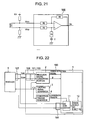
- FIG. 21 shows another embodiment of the frequency-division input means 106 in which the gain for DC region is fixed at 1.
- the input/output relation for DC region is as follows.
- the input means operates as a differential input configuration and for DC region the input means operates as a single-end input configuration of gain 1.
- the gain for DC region can be fixed at 1
- the center values of the signals in the differential input means 103, frequency-division input means 106 and the following-stage A/D converter 11 can be set to be the optimum points for treating the maximum amplitude, or 1/2 the operating source voltage to the circuits.
- FIG. 22 shows an embodiment of the invention in which it is prevented that, if the center voltages (bias voltages) of the signals Y sin , Y cos are made different in order to detect the inter-phase short circuit between the signals Y sin , Y cos , the center voltage (bias voltage) of the input signal to the resolver/digital converter 2 may be deviated from an ideal value (for example, 2.5 V) to cause the waveforms of the upper and lower ends of the signal to be clipped due to the saturation, thus limiting the maximum amplitude.
- a bias applying circuit 107 is provided to apply different center voltages (bias voltages) to the signals Y sin , Y cos .
- a bias correcting circuit 108 adds a correction bias to correct the center voltages (bias voltages) into an ideal value (for example, 2.5 V), and supplies the corrected signals to the normal mode input means 101 or differential input means 103 that are placed at the input stage of the resolver/digital converter 2. Therefore, when the inter-phase short circuit does not occur, the signals Y sin , Y cos fed to the resolver/digital converter 2 have an ideal value (for example, 2.5 V) as their center voltage (bias voltage) since they are corrected after predetermined different center voltages (bias voltages) are added to the resolver signals, and thus those signals have the ideal value (for example, 2.5 V) as the center voltage (bias voltage).
- the center voltages applied to the signals Y sin , Y cos are deviated from a certain value, and thus the signals Y sin , Y cos fed to the resolver/digital converting portion 2 also have the center voltages (bias voltages) deviated from the ideal value (for example, 2.5 V) so that the inter-phase short circuit occurrence can be detected.
- the resolver signals are received by the differential input means but not the single-end input means, the waveforms of the upper and lower ends of the signal of a narrow input voltage range are clipped due to saturation, and thus the inter-phase short circuit can be detected as abnormal waveforms.
- This embodiment functions effectively when the input voltage range to the resolver/digital converting portion 2 is narrow. However, when the input voltage range to the A/D converter 11 or common mode input means 102 or single-end input means 104 is narrow, the bias correcting circuit 108 is similarly needed to place before the common mode input means 102 or single-end input means 104.
- FIG. 23 shows an example of the frequency characteristic of the frequency division input means 106 that takes the single-end input configuration for the frequency region around the resolver signal frequency.
- This example is effective particularly when the region around the resolver signal frequency is little affected by noise, but when the other frequency regions are much affected by noise. For example, this corresponds to the case when the switching frequency of the PWM inverter for driving the motor that is the main noise source is much lower or much higher than the resolver signal frequency.
- the first method is that a filter for eliminating the frequency region around the resolver signal frequency is inserted in one of the two input lines of the differential input circuit.
- the differential input means functions for the other frequency regions.
- the second method is that a high-pass filter with a cutoff frequency sufficiently lower than the resolver signal frequency is inserted in one of the two input lines of the differential input circuit and that another high-pass filter with a cutoff frequency sufficiently higher than the resolver signal frequency is inserted in the other line.
- the differential input means functions for the frequency band higher than the resolver signal frequency region, but the lower frequency band than the resolver signal frequency region is cut off.
- the third method is that a low-pass filter with a cutoff frequency sufficiently lower than the resolver signal frequency is inserted in one of the two input lines of the differential input circuit and that a low-pass filter with a cutoff frequency sufficiently higher than the resolver signal frequency is inserted in the other line.
- the differential input means operates for the lower frequency band than the resolver signal frequency region, but the higher frequency band than the resolver signal frequency region is cut off.
- FIG. 24 shows an example of the circuits for implementing the second method.
- the cutoff frequency of the high-pass filter can be substantially determined by the time constants of C 1 ⁇ Ri, C 2 . R i .
- a control system can be achieved that is not affected by the inter-phase short but that can detect the inter-phase short.
- the failure (1) of the abnormality of waveforms due to the disconnection of the signal from or to the resolver can be detected by the failure detecting function provided in the resolver/digital converter 2 and the error detecting function 12 of the invention.
- the failure (2) of the function to detect the failure (1) and notify the microcomputer can be detected by the other function even if one function breaks down.
- the failure (3) of the resolver/digital converter function itself for finding ⁇ on the basis of the signal from the resolver can be detected by the failure detecting function provided in the resolver/digital converting portion 2 and the error detecting function 12 of the invention.
- the failure (4) of the function to detect the failure (3) and notify the microcomputer can also be detected by the other function even if one function goes out of order.
- the failures of the resolver and resolver/digital converter can be detected. If a failure is detected in the application to the motor-driven power steering apparatus or the like, the motor-driven assist mechanism is stopped, thus the fail-safe operation being assured. In addition, since the system operation is not allowed to stop in x-by-write, particularly steer-by-wire or fly-by-wire, the fault tolerance is demanded that can continue the operation even when a failure occurs. Thus, as illustrated in FIG. 26 , if resolvers 5-1, 5-2 and resolver/digital converting portions 2-1, 2-2 are doubly provided, and combined with the error detecting function 12, a triple system can be substantially achieved to form a fault tolerance system.
- the failure can be detected by the failure detecting function provided in the resolver/digital converting portions 2-1, 2-2 and the error detecting function 12, and the defective portion can be located. Then, the failure-free ones of the double resolvers 5-1, 5-2, resolver/digital converting portions 2-1, 2-2 can be used to maintain the operations. It would be further desirable to make the microcomputer 1 be a multiple structure.
- FIG. 27 shows an embodiment of a motor control system according to the invention.
- the microcomputer 1 is responsive to the estimated angle ⁇ from the resolver/digital converting portion 2 to supply a motor-drive command to a timer 6 that generates a PWM signal.
- the timer 6 responds to the command from the microcomputer 1 to generate the PWM signal of a predetermined duty cycle.
- a motor driver 7 drives a motor 8 according to the waveform of the PWM signal.
- the output shaft of motor 8 is connected to a controlled object 9 and thus moves the controlled object 9.
- the output shaft of the motor is also connected to the resolver 5 by which the rotation angle is measured.
- the rotation angle is supplied to the microcomputer 1.
- the controlled object 9 is the whole steering system.
- the controlled object 9 is the steering column and steering mechanism (steerage apparatus).
- a torque monitoring function 14 is used to monitor the torque signal from a torque sensor 13, thus further improving the safety.
- the function of power steering apparatus is to assist the steerage by motive energy and to thereby alleviate the driver's steering force.
- the driver should exert an unusual steering force (torque) against this operation.
- the torque monitoring function 14 detects the driver's unusual steering force (torque) when the power steering apparatus breaks down, and stops the assist mechanism, thus assuring the failsafe operation.
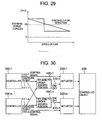
- the steering force When the steering force is aided by the power steering, the steering force (torque) is substantially 2 to 3 (Nm), but when the driver widely turns the steering wheel, it is about 15 (Nm). Therefore, when the driver exerts a steering force (torque) that exceeds 20 to 30 (Nm) including a margin, the power steering apparatus is regarded as being broken down, and the assist mechanism is stopped so that the failsafe operation can be assured.
- various thresholds to the steering force (torque) are provided for the detection of the abnormality in different speeds of car as shown in FIG. 29 .
- the threshold is stepwise changed in accordance with the speed range of car.
- the threshold is selected to be 5 to 6 (Nm) and for low speed it is fixed to 20 to 30 (Nm).
- Nm 5 to 6
- Nm 20 to 30
- FIG. 30 shows an embodiment of a redundant-structure control apparatus. Redundant multiple controllers 100-1 to 100-n supply control signals 110-1 to 110-n as control commands to actuators 200-1 to 200-n. The controllers 100-1 to 100-n also produce the results 111-1 to 111-n of their own diagnosis. Reliability order judging portions 400-1 to 400-n produce ON/OFF signals 410-1 to 400-n on the basis of the diagnosis results 111-1 to 111-n supplied from the controllers 100-1 to 100-n.
- the actuator 200-i when the input ON/OFF signal 410-i is ON, controls a controlled object 300 to act by the amount based on the inputted control signal 110-i.
- the input ON/OFF signal 410-i is OFF, it does not control the controlled object 300.
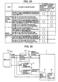
- FIG. 31 shows a table of the judgment in the reliability order judging portions 400-1 to 400-n, or the relation between the diagnosis result 111-1 to 111-n and the ON/OFF signal 410-1 to 410-n.
- the ON/OFF signal 410-i of interest is turned ON.
- the ON/OFF signal 410-i of interest is turned OFF.
- the diagnosis result 111-i of interest has no failure, and thus the ON/OFF signal 410-i of interest is turned ON.
- the diagnosis result 111-i of interest has a minor failure, but the diagnosis results 111-j of the other objects also have a minor failure, and thus the ON/OFF signal 410-i of interest is turned ON.
- the case 3 is taken, the diagnosis results 111-j of the other objects have no failure, but the diagnosis result 111-i of interest has a minor failure, thus the ON/OFF signal 410-i of interest being turned OFF.
- both the diagnosis result 111-i of interest and the diagnosis results 111-j of the other objects have middle failures, and thus the ON/OFF signal 410-i of interest is turned ON.
- the diagnosis results 111-j of the other objects have middle failure, but the diagnosis result 111-i of interest has a serious failure, thus the ON/OFF signal 410-i of interest being turned OFF.
- the ON/OFF signal 410-i of interest is turned OFF irrespective of what degree the diagnosis results of the other objects show. If the case 6 is taken, the diagnosis result 111-i of interest shows a serious failure, and thus the ON/OFF signal 410-i of interest is turned OFF independently of the diagnosis results 111-j of the other objects.
- FIG. 32 shows an example of the definition of failure grades.
- the grades of failure can be classified according to the scale of the function lost due to the failure or to the probability of the occurrence of failure indicated by the diagnosis result.
- the degrees of failure in the sensor are classified according to the scale of the function lost due to the failure of the sensor in the former case.
- the memory can be recovered from failure by the error correction code (ECC)
- ECC error correction code
- the degrees of failure in the memory can be classified according to the possibility of recovery, or to the probability of the occurrence of failure indicated by the diagnosis result in the latter case.
- the degrees of failure in the processor can be classified as minor or middle according to the probability of failure occurrence indicated by the diagnosis result, and as serious when the processor function is seriously damaged.
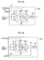
- FIGS. 33 through 36 are block diagrams showing embodiments of the invention in which the operation of actuator 200-i is controlled by using ON/OFF signal 410-i.
- FIG. 33 shows an embodiment in which the ON/OFF signal 410-i controls a main switch 211 for the power supply to the actuator 200-i that drives a motor 210 by use of an inverter formed of semiconductor devices 201 to 206.
- the ON/OFF signal 410-i is ON, the main switch 211 is closed, and the inverter formed of semiconductor devices 201 to 206 in the actuator 200-i is actuated according to the control signal 110-i to drive the motor 210.
- the ON/OFF signal 410-i is OFF, the main switch 211 is opened, and the inverter of semiconductor devices 201 to 206 is stopped from producing the output, thus ceasing to drive the motor 20.
- FIG. 34 shows an embodiment in which a switch 212 is opened or closed by the ON/OFF signal 410-i to allow the inverter to supply or not to supply the output to the motor 210.
- the ON/OFF signal 410-i is ON
- the switch 212 is closed, and the inverter of semiconductor devices 201 to 206 in the actuator 200-i is actuated by the control signal 110-i to drive the motor 210.
- the ON/OFF signal 410-i is OFF, the switch 212 is opened, and the inverter of semiconductor devices 201 to 206 is stopped from producing the output, thus ceasing to drive the motor 210.
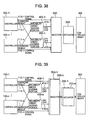
- FIG. 35 shows an embodiment in which a logical product (AND) 213 is used to control the gate signals to the semiconductor devices 201 to 206 on the basis of the ON/OFF signal 410-i.
- a logical product (AND) 213 is used to control the gate signals to the semiconductor devices 201 to 206 on the basis of the ON/OFF signal 410-i.
- the ON/OFF signal 410-i is ON
- the inverter of semiconductor devices 201 to 206 is actuated by the control signal 110-i to drive the motor 210.
- the ON/OFF signal 410-i is OFF
- the gate signals to the semiconductors 201 to 206 are always OFF, and thus the inverter is stopped from producing the output, thus ceasing to drive the motor 210.
- FIG. 36 shows an embodiment in which a clutch 214 is provided on the output shaft of motor 210 and intermitted according to the ON/OFF signal 410-i.
- the ON/OFF signal 410-i is ON, the clutch 214 is fastened, and thus the power of the motor 210 is, when the motor is driven, transmitted through its output shaft to the outside.
- the ON/OFF signal 410-i is OFF, the clutch 214 is opened, and thus the output power of the motor 210 is not transmitted through the output shaft.
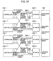
- FIG. 37 shows an embodiment in which this invention is applied to brakes.
- the right front brake and right back brake of the controlled object (automobile) 300 are controlled by a doubled control apparatus formed of a set of controllers 100-1, 100-2, actuators 200-1, 200-2, and reliability order judging portions 400-1, 400-2.
- the left front brake and left back brake of the controlled object (automobile) 300 are controlled by another doubled control apparatus formed of a set of controllers 100-3, 100-4, actuators 200-3, 200-4, and reliability order judging portions 400-3, 400-4.
- the right back brake is continuously controlled by the controller 100-2, actuator 200-2 and reliability order judging portion 400-2 even if a minor failure occurs in any one of the devices 100-2, 200-2 and 400-2 so that the right brakes of the controlled object (automobile) 300 can be maintained to operate, exerting a certain braking force without causing yaw moment.
- the same action is taken even if a serious failure occurs in the controller 100-2 ⁇ 100-4, actuator 200-1 ⁇ 200-4, or reliability order judging portion 400-1 ⁇ 400-4.
- FIG. 38 shows an embodiment in which the control signals 110-1, 110-2 are switched by a selector 500 and supplied to a single actuator 200.
- the selector 500 may be Modified Votor (MV) described in Patent 2085879 that the inventor already filed.
- selectors 500-1 ⁇ 500-n, and actuators 200-1 ⁇ 200-n can be redundantly provided as illustrated in FIG. 39 .
Landscapes
- Engineering & Computer Science (AREA)
- Transportation (AREA)
- Mechanical Engineering (AREA)
- Physics & Mathematics (AREA)
- General Physics & Mathematics (AREA)
- Chemical & Material Sciences (AREA)
- Combustion & Propulsion (AREA)
- Theoretical Computer Science (AREA)
- Automation & Control Theory (AREA)
- Transmission And Conversion Of Sensor Element Output (AREA)
- Valves And Accessory Devices For Braking Systems (AREA)
- Power Steering Mechanism (AREA)
Claims (17)
- Resolver/Digital-Wandler mit:einem Resolver (5), der Signale erzeugt;einer Erregungssignalquelle (3), die ein Erregungssignal erzeugt und das Erregungssignal dem Resolver zuführt;einem A/D-Wandler (11), der die Resolversignale in digitale Werte umwandelt;einem Berechnungsbereich (12), der einen Ausfall unter Verwendung der Ausgabe von dem A/D-Wandler (11) erfasst, undeiner Wandlungstriggerquelle (4), die einen Wandlungstrigger nach Maßgabe des Erregungssignals erzeugt, wobei der A/D-Wandler (11) die Resolversignale als Reaktion auf den Wandlungstrigger in digitale Werte umwandelt,dadurch gekennzeichnet, dass er weiterhin Folgendes umfasst:einen Resolver/Digital-Wandlungsbereich (2), der die von dem Resolver erzeugten Resolversignale empfängt;wobei der Berechnungsbereich (12) Werte von Sinus und Kosinus oder Tangens auf der Grundlage der digitalen Werte von dem A/D-Wandler (11) berechnet und beurteilt, dass ein Ausfall vorliegt, wenn die Differenzen der Werte von Sinus, Kosinus oder Tangens zu denjenigen eines geschätzten Winkels, der von dem Resolver/Digital-Wandlungsbereich (2) ermittelt wird, vorgegebene Werte überschreiten.
- Resolver/Digital-Wandler nach Anspruch 1, wobei die Wandlungstriggerquelle (4) das von der Erregungssignalquelle (3) erzeugte Erregungssignal mit einer Bezugsspannung vergleicht, um den Wandlungstrigger zu erzeugen.
- Resolver/Digital-Wandler nach Anspruch 1, wobei die Wandlungstriggerquelle (4) einen Nulldurchgangspunkt des von der Erregungssignalquelle (3) erzeugten Erregungssignals erfasst und den Wandlungstrigger eine vorgegebene Verzögerungszeit nach dem Nulldurchgangspunkt erzeugt.
- Resolver/Digital-Wandler nach Anspruch 1, wobei die Wandlungstriggerquelle (4) eine Spitze des von der Erregungssignalquelle (3) erzeugten Erregungssignals erfasst, um den Wandlungstrigger zu erzeugen.
- Resolver/Digital-Wandler nach Anspruch 1, wobei die Wandlungstriggerquelle (4) das von der Erregungssignalquelle (3) erzeugte Erregungssignal unter Verwendung eines Phasenschiebers (45) verzögert, einen Nulldurchgangspunkt erfasst und den Wandlungstrigger eine vorgegebene Verzögerungszeit nach dem Nulldurchgangspunkt erzeugt.
- Resolver/Digital-Wandler nach Anspruch 1, wobei der Berechnungsbereich (12) Werte von Sinus, Kosinus oder Tangens auf der Grundlage der digitalen Werte von dem A/D-Wandler (11) berechnet, entsprechende Winkel aus den berechneten Werten von Sinus und Kosinus oder Tangens berechnet und beurteilt, dass ein Ausfall vorliegt, wenn die Differenzen zwischen den Winkeln vorgegebene Werte überschreiten.
- Resolver/Digital-Wandler nach Anspruch 1, wobei der Resolver/Digital-Wandlungsbereich (2) Mittel zum Empfangen von Gleichtaktkomponenten (102) der Resolversignale und Mittel zum Empfangen von Gegentaktkomponenten (101) der Resolversignale aufweist.
- Resolver/Digital-Wandler nach Anspruch 1, wobei der Resolver/Digital-Wandlungsbereich Mittel zum Empfangen der Resolversignale in einer differenziellen Weise (103) und Mittel zum Empfangen der Resolversignale in einer einfachwirkenden Weise (104) aufweist.
- Resolver/Digital-Wandler nach Anspruch 1, mit einem Mikrocomputer (1), der einen von dem Resolver/Digital-Wandlungsbereich (2) erzeugten geschätzten Winkel empfängt, wobei der A/D-Wandler (11) und der Berechnungsbereich (12) in dem Mikrocomputer vorgesehen sind.
- Resolver/Digital-Wandler nach Anspruch 9, wobei der Resolver/Digital-Wandlungsbereich (2) dem Mikrocomputer (1) ein Fehlererfassungssignal zuführt.
- Resolver/Digital-Wandler nach Anspruch 1, wobei der Resolver (5) und der Resolver/Digital-Wandlungsbereich (2) jeweils redundant verdoppelt sind.
- Motorsteuerungsvorrichtung, in der ein Resolver/DigitalWandler nach Anspruch 1 verwendet wird und der Berechnungsbereich einen Wert von elektrischem Strom berechnet, der in einem Motor (8) zum Fließen gebracht werden soll, und den Strom des Werts dem Motor zuführt, wobei die Ausgangswelle des Motors mit einem gesteuerten Objekt (9) und dem Resolver verbunden ist.
- Motorbetriebene Lenkhilfevorrichtung, bei der eine Motorsteuerungsvorrichtung gemäß Anspruch 12 verwendet wird und das gesteuerte Objekt (9) ein Lenkmechanismus ist.
- Steer-by-wire-Steuerungsvorrichtung, bei der eine Motorsteuerungsvorrichtung gemäß Anspruch 12 verwendet wird und das gesteuerte Objekt (9) eine Lenksäule und ein Lenkmechanismus ist.
- Motorbetriebene Lenkhilfevorrichtung nach Anspruch 13, bei der ein Drehmomentsensor (13) zum Erfassen eines Lenkdrehmoments verwendet wird und eine Lenkkraft nach Maßgabe des Lenkdrehmoments unterstützt wird, wobei die Unterstützung für die Lenkkraft gestoppt wird, wenn das von dem Drehmomentsensor erfasste Lenkdrehmoment eine vorgegebene Schwelle übersteigt.
- Motorbetriebene Lenkhilfevorrichtung nach Anspruch 15, wobei die Unterstützung für die Lenkkraft gestoppt wird, wenn das von dem Drehmomentsensor erfasste Lenkdrehmoment während einer vorgegebenen Zeit oder darüber die Schwelle weiterhin übersteigt.
- Motorbetriebene Lenkhilfevorrichtung nach Anspruch 15, wobei die Schwelle mit der Änderung der Fahrzeuggeschwindigkeit geändert wird.
Priority Applications (1)
| Application Number | Priority Date | Filing Date | Title |
|---|---|---|---|
| EP10002937A EP2228696A1 (de) | 2004-01-28 | 2005-01-27 | Resolver/Digital-Wandler und Steuergerät mit Hilfe eines solchen Wandlers |
Applications Claiming Priority (6)
| Application Number | Priority Date | Filing Date | Title |
|---|---|---|---|
| JP2004020368 | 2004-01-28 | ||
| JP2004020368 | 2004-01-28 | ||
| JP2004108614 | 2004-04-01 | ||
| JP2004108614 | 2004-04-01 | ||
| JP2004350551A JP4521258B2 (ja) | 2004-01-28 | 2004-12-03 | レゾルバ/デジタル変換器及びこれを用いた制御システム |
| JP2004350551 | 2004-12-03 |
Related Child Applications (1)
| Application Number | Title | Priority Date | Filing Date |
|---|---|---|---|
| EP10002937.0 Division-Into | 2010-03-19 |
Publications (4)
| Publication Number | Publication Date |
|---|---|
| EP1560085A2 EP1560085A2 (de) | 2005-08-03 |
| EP1560085A3 EP1560085A3 (de) | 2005-09-07 |
| EP1560085B1 true EP1560085B1 (de) | 2010-05-12 |
| EP1560085B8 EP1560085B8 (de) | 2010-06-23 |
Family
ID=34657751
Family Applications (2)
| Application Number | Title | Priority Date | Filing Date |
|---|---|---|---|
| EP05001744A Expired - Lifetime EP1560085B8 (de) | 2004-01-28 | 2005-01-27 | Resolver/Digital-Wandler und Steuergerät mit Hilfe eines solchen Wandlers |
| EP10002937A Withdrawn EP2228696A1 (de) | 2004-01-28 | 2005-01-27 | Resolver/Digital-Wandler und Steuergerät mit Hilfe eines solchen Wandlers |
Family Applications After (1)
| Application Number | Title | Priority Date | Filing Date |
|---|---|---|---|
| EP10002937A Withdrawn EP2228696A1 (de) | 2004-01-28 | 2005-01-27 | Resolver/Digital-Wandler und Steuergerät mit Hilfe eines solchen Wandlers |
Country Status (4)
| Country | Link |
|---|---|
| US (2) | US6972700B2 (de) |
| EP (2) | EP1560085B8 (de) |
| JP (1) | JP4521258B2 (de) |
| DE (1) | DE602005021174D1 (de) |
Cited By (2)
| Publication number | Priority date | Publication date | Assignee | Title |
|---|---|---|---|---|
| DE102014100624A1 (de) * | 2014-01-21 | 2015-07-23 | Phoenix Contact Gmbh & Co. Kg | Resolver-Anordnung |
| CN107921994A (zh) * | 2015-09-09 | 2018-04-17 | 罗伯特博世汽车转向有限公司 | 用于运行伺服转向系统的装置以及伺服转向系统 |
Families Citing this family (64)
| Publication number | Priority date | Publication date | Assignee | Title |
|---|---|---|---|---|
| JP4294558B2 (ja) * | 2004-08-23 | 2009-07-15 | ソニー株式会社 | 角度検出信号処理装置 |
| JP4627746B2 (ja) | 2005-07-19 | 2011-02-09 | 日立オートモティブシステムズ株式会社 | 位相検出回路及びこれを用いたレゾルバ/デジタル変換器並びに制御システム |
| JP4765779B2 (ja) * | 2005-07-19 | 2011-09-07 | 株式会社デンソー | 制御装置,ショート検出装置,負荷駆動システムおよびプログラム |
| DE602006003954D1 (de) * | 2005-08-11 | 2009-01-15 | Mitutoyo Corp | Verfahren und Schaltungsanordnung zur Interpolation des Ausgangssignals eines Kodierers |
| DE102006046286A1 (de) * | 2005-12-16 | 2007-06-21 | Siemens Ag | Bewegungsüberwachung |
| US7286068B2 (en) * | 2005-12-30 | 2007-10-23 | Honeywell International Inc. | Method and system for detecting failures in an analog-to-digital converter |
| JP4979352B2 (ja) * | 2006-02-28 | 2012-07-18 | 日立オートモティブシステムズ株式会社 | レゾルバ/デジタル変換器及び該レゾルバ/デジタル変換器を用いた制御システム |
| JP4991322B2 (ja) | 2006-10-30 | 2012-08-01 | 日立オートモティブシステムズ株式会社 | Gmr素子を用いた変位センサ,gmr素子を用いた角度検出センサ及びそれらに用いる半導体装置 |
| GB2447901B (en) * | 2007-03-26 | 2011-06-01 | Qatar University | Apparatus for the determination of the angle from sine/cosine transducers |
| GB2448350B (en) * | 2007-04-12 | 2011-06-01 | Qatar University | PLL type resolver to 360 degrees linear converter apparatus |
| US7863850B2 (en) * | 2007-05-11 | 2011-01-04 | GM Global Technology Operations LLC | Apparatus, system, and method for simulating outputs of a resolver to test motor-resolver systems |
| US7834576B2 (en) * | 2007-05-14 | 2010-11-16 | Gm Global Technology Operations, Inc. | Apparatus and methods for diagnosing motor-resolver system faults |
| JP5063495B2 (ja) * | 2007-08-08 | 2012-10-31 | 日立オートモティブシステムズ株式会社 | 角度検出回路 |
| JP2009040193A (ja) * | 2007-08-08 | 2009-02-26 | Jtekt Corp | 電動パワーステアリング装置のモータ制御装置 |
| JP4863953B2 (ja) | 2007-08-30 | 2012-01-25 | 日立オートモティブシステムズ株式会社 | 物理量変換センサ及びそれを用いたモータ制御システム |
| JP4950824B2 (ja) * | 2007-09-28 | 2012-06-13 | 株式会社東芝 | 回転機の制御装置、制御システムおよび制御方法 |
| JP4929189B2 (ja) | 2008-01-09 | 2012-05-09 | 日立オートモティブシステムズ株式会社 | レゾルバ異常検出回路 |
| JP5028294B2 (ja) * | 2008-02-14 | 2012-09-19 | 日立オートモティブシステムズ株式会社 | レゾルバの異常検出装置 |
| JP5125711B2 (ja) * | 2008-04-14 | 2013-01-23 | 株式会社ジェイテクト | トルク検出装置及び電動パワーステアリング装置 |
| US20100001670A1 (en) * | 2008-07-03 | 2010-01-07 | Honeywell International Inc., | Single-chip brushless motor controller |
| US7877231B2 (en) * | 2008-07-22 | 2011-01-25 | Honeywell International Inc. | Electromechanical actuator and effector health management system and method |
| US7977936B2 (en) * | 2008-10-16 | 2011-07-12 | Hamilton Sundstrand Corporation | Resolver interface and signal conditioner |
| JP2010152595A (ja) * | 2008-12-25 | 2010-07-08 | Omron Corp | サーボシステムおよび安全制御機器 |
| US7969229B2 (en) | 2009-02-19 | 2011-06-28 | Hitachi, Ltd. | On-chip redundancy high-reliable system and method of controlling the same |
| WO2010138155A2 (en) * | 2009-05-27 | 2010-12-02 | Active Precision, Inc. | Encoder interpolator with enhanced precision |
| US8269445B2 (en) * | 2009-10-20 | 2012-09-18 | GM Global Technology Operations LLC | Limp home operational mode for an electric vehicle |
| KR101039676B1 (ko) * | 2009-11-04 | 2011-06-09 | 현대자동차주식회사 | 하이브리드 차량의 레졸버 단락 및 단선 감지용 회로 및 이를 이용한 레졸버 단락 및 단선 감지 방법 |
| DE102011009720A1 (de) | 2010-02-02 | 2011-08-04 | Daimler AG, 70327 | Drehmelder-Baugruppe und Verfahren zur Bestimmung der Winkellage eines Rotors |
| JP5086385B2 (ja) * | 2010-03-08 | 2012-11-28 | 日立オートモティブシステムズ株式会社 | 電動パワーステアリング制御装置 |
| WO2011158876A1 (ja) | 2010-06-18 | 2011-12-22 | 日立オートモティブシステムズ株式会社 | 電子制御装置 |
| US9046891B2 (en) | 2010-10-22 | 2015-06-02 | Honeywell International Inc. | Control effector health capabilities determination reasoning system and method |
| DE102011014317B4 (de) | 2011-03-18 | 2021-07-29 | Robert Bosch Gmbh | Sensorüberwachung einer Positionsmessvorrichtung mittels Wärmerauschen |
| WO2012155089A2 (en) * | 2011-05-12 | 2012-11-15 | Saez Carlos A | Method and apparatus for variable reduced effort steering in electric steering systems |
| US8432185B2 (en) * | 2011-05-25 | 2013-04-30 | Apple Inc. | Receiver circuits for differential and single-ended signals |
| US8410814B2 (en) * | 2011-06-16 | 2013-04-02 | Apple Inc. | Receiver circuits for differential and single-ended signals |
| US8988025B2 (en) * | 2012-01-20 | 2015-03-24 | GM Global Technology Operations LLC | Systems and methods for controlling a brushless motor |
| JP6106839B2 (ja) * | 2012-02-10 | 2017-04-05 | パナソニックIpマネジメント株式会社 | エンコーダ |
| JP2013200173A (ja) * | 2012-03-23 | 2013-10-03 | Jtekt Corp | レゾルバ/デジタル変換器 |
| RU2488958C1 (ru) * | 2012-06-14 | 2013-07-27 | Открытое акционерное общество "Центральный научно-исследовательский институт автоматики и гидравлики" (ОАО "ЦНИИАГ") | Способ цифрового преобразования угла |
| JP5892012B2 (ja) * | 2012-09-11 | 2016-03-23 | 日本精工株式会社 | 車載電子制御装置 |
| JP6233881B2 (ja) * | 2013-12-27 | 2017-11-22 | 日立オートモティブシステムズ株式会社 | 回転角検出装置 |
| KR101619593B1 (ko) * | 2014-07-08 | 2016-05-10 | 현대자동차주식회사 | 레졸버 고장판단 방법 |
| KR101583957B1 (ko) * | 2014-07-28 | 2016-01-08 | 현대자동차주식회사 | 레졸버 오결선 검출 방법 |
| US10187067B2 (en) | 2014-10-14 | 2019-01-22 | Qatar University | Phase-locked loop (PLL)-type resolver/converter method and apparatus |
| JP2016163454A (ja) * | 2015-03-03 | 2016-09-05 | トヨタ自動車株式会社 | モータ制御装置 |
| RU2598309C1 (ru) * | 2015-06-08 | 2016-09-20 | Закрытое акционерное общество "Орбита" | Способ определения угла поворота ротора датчика угла типа синусно-косинусного вращающегося трансформатора |
| DE102015211224A1 (de) * | 2015-06-18 | 2016-12-22 | Robert Bosch Gmbh | Verfahren und Schaltung zum Erkennen einer offenen Resolver-Erregerleitung |
| US9935646B2 (en) | 2015-07-17 | 2018-04-03 | Schweitzer Engineering Laboratories, Inc. | Systems and methods for identifying a failure in an analog to digital converter |
| US9584148B1 (en) * | 2016-01-19 | 2017-02-28 | Schweitzer Engineering Laboratories, Inc. | Systems and methods for analog to digital converter failure identification |
| US10408643B2 (en) * | 2016-08-18 | 2019-09-10 | Texas Instruments Incorporated | Methods and apparatus to increase resolver-to-digital converter accuracy |
| JP6689712B2 (ja) * | 2016-08-23 | 2020-04-28 | ルネサスエレクトロニクス株式会社 | レゾルバ補正装置及び半導体装置 |
| JP6732238B2 (ja) * | 2016-10-19 | 2020-07-29 | 多摩川精機株式会社 | アナログ信号をディジタル信号に変換する方法および装置 |
| JP6732237B2 (ja) * | 2016-10-19 | 2020-07-29 | 多摩川精機株式会社 | アナログ信号をディジタル信号に変換する方法および装置 |
| KR101897640B1 (ko) * | 2016-12-12 | 2018-09-12 | 현대오트론 주식회사 | 레졸버 고장 진단 장치 및 방법 |
| US10033400B1 (en) | 2017-10-18 | 2018-07-24 | Schweitzer Engineering Laboratories, Inc. | Analog-to-digital converter verification using quantization noise properties |
| US9985646B1 (en) | 2017-10-18 | 2018-05-29 | Schweitzer Engineering Laboratories, Inc. | Analog-to-digital converter verification using quantization noise properties |
| KR102019384B1 (ko) * | 2018-03-19 | 2019-09-06 | 현대오트론 주식회사 | 레졸버 관리 장치, 그것을 포함하는 레졸버 시스템 및 그것의 동작 방법 |
| US11215477B2 (en) * | 2020-03-11 | 2022-01-04 | Hamilton Sundstrand Corporation | Motor control systems for multiple motor drives |
| WO2021240191A1 (ja) * | 2020-05-28 | 2021-12-02 | 日産自動車株式会社 | 監視制御装置及び監視制御方法 |
| CN112485460B (zh) * | 2020-11-17 | 2022-11-04 | 上海吉亿电机有限公司 | 旋转变压器信号采集及补偿方法 |
| KR102415786B1 (ko) * | 2020-12-09 | 2022-07-04 | 현대모비스 주식회사 | 신호 처리 장치 및 방법, 레졸버 반도체 |
| US11662224B2 (en) | 2021-08-30 | 2023-05-30 | Delphi Technologies Ip Limited | Systems and methods for fail-safe resolver excitation |
| KR102910368B1 (ko) * | 2024-03-07 | 2026-01-09 | 에이치엘만도 주식회사 | 차량 주행 시 고장 검출 시간 설정 장치 및 방법 |
| CN120439996B (zh) * | 2025-07-04 | 2025-10-28 | 重庆长安汽车股份有限公司 | 一种车辆的轮速控制系统及方法 |
Family Cites Families (22)
| Publication number | Priority date | Publication date | Assignee | Title |
|---|---|---|---|---|
| US4134106A (en) * | 1976-12-16 | 1979-01-09 | The Bendix Corporation | Absolute resolver angle to digital converter circuit |
| DE3328548A1 (de) | 1983-08-08 | 1985-02-21 | Kraftanlagen Ag, 6900 Heidelberg | Speichermaterial fuer waermeuebertragung |
| US4651130A (en) * | 1985-08-28 | 1987-03-17 | United Technologies Corporation | Apparatus and method for retaining phase information for use with a multiple-coil inductive displacement sensor |
| US5015934A (en) * | 1989-09-25 | 1991-05-14 | Honeywell Inc. | Apparatus and method for minimizing limit cycle using complementary filtering techniques |
| US5229697A (en) * | 1992-01-30 | 1993-07-20 | Siemens Industrial Automation, Inc. | Sampling bipolar peak detector for sensing a non-symmetrical decay of an AC voltage signal |
| JPH05346434A (ja) * | 1992-06-15 | 1993-12-27 | Komatsu Ltd | レゾルバの駆動制御装置 |
| US5347277A (en) * | 1992-09-30 | 1994-09-13 | Allen-Bradley Company, Inc. | Dual phase resolver to digital converter |
| JP3216491B2 (ja) * | 1995-09-08 | 2001-10-09 | トヨタ自動車株式会社 | レゾルバ異常検出装置及び方法 |
| US6552666B1 (en) * | 1996-03-16 | 2003-04-22 | Atsutoshi Goto | Phase difference detection device and method for a position detector |
| JPH09280890A (ja) | 1996-04-11 | 1997-10-31 | Mitsubishi Electric Corp | シンクロ/デジタル変換器 |
| US6161051A (en) * | 1998-05-08 | 2000-12-12 | Rockwell Technologies, Llc | System, method and article of manufacture for utilizing external models for enterprise wide control |
| US6157864A (en) * | 1998-05-08 | 2000-12-05 | Rockwell Technologies, Llc | System, method and article of manufacture for displaying an animated, realtime updated control sequence chart |
| JP3368837B2 (ja) * | 1998-08-05 | 2003-01-20 | トヨタ自動車株式会社 | レゾルバ信号処理装置 |
| JP2000235019A (ja) * | 1999-02-12 | 2000-08-29 | Genshiryoku Engineering:Kk | 渦流探傷プローブ |
| JP3442316B2 (ja) * | 1999-06-11 | 2003-09-02 | 多摩川精機株式会社 | アナログ信号のディジタル変換方法 |
| US6556950B1 (en) * | 1999-09-30 | 2003-04-29 | Rockwell Automation Technologies, Inc. | Diagnostic method and apparatus for use with enterprise control |
| JP2001349748A (ja) * | 2000-06-09 | 2001-12-21 | Minebea Co Ltd | レゾルバ、レゾルバ故障検出回路およびレゾルバ故障検出方法 |
| JP2002091569A (ja) * | 2000-07-11 | 2002-03-29 | Harmonic Drive Syst Ind Co Ltd | アブソリュートセンサを用いた位置決めシステム |
| JP3630410B2 (ja) * | 2001-05-22 | 2005-03-16 | 三菱電機株式会社 | 位置検出装置および異常検出装置 |
| JP3644922B2 (ja) * | 2001-12-06 | 2005-05-11 | 本田技研工業株式会社 | 電動パワーステアリング装置 |
| JP2005114442A (ja) * | 2003-10-06 | 2005-04-28 | Hitachi Ltd | 故障検出機能付レゾルバ/デジタル変換器 |
| JP2006017659A (ja) * | 2004-07-05 | 2006-01-19 | Tamagawa Seiki Co Ltd | アナログ信号のデジタル変換方法 |
-
2004
- 2004-12-03 JP JP2004350551A patent/JP4521258B2/ja not_active Expired - Lifetime
-
2005
- 2005-01-27 DE DE602005021174T patent/DE602005021174D1/de not_active Expired - Lifetime
- 2005-01-27 US US11/043,639 patent/US6972700B2/en not_active Expired - Lifetime
- 2005-01-27 EP EP05001744A patent/EP1560085B8/de not_active Expired - Lifetime
- 2005-01-27 EP EP10002937A patent/EP2228696A1/de not_active Withdrawn
- 2005-08-26 US US11/211,506 patent/US7009535B2/en not_active Expired - Lifetime
Cited By (3)
| Publication number | Priority date | Publication date | Assignee | Title |
|---|---|---|---|---|
| DE102014100624A1 (de) * | 2014-01-21 | 2015-07-23 | Phoenix Contact Gmbh & Co. Kg | Resolver-Anordnung |
| DE102014100624B4 (de) * | 2014-01-21 | 2017-04-06 | Phoenix Contact Gmbh & Co. Kg | Resolver-Anordnung |
| CN107921994A (zh) * | 2015-09-09 | 2018-04-17 | 罗伯特博世汽车转向有限公司 | 用于运行伺服转向系统的装置以及伺服转向系统 |
Also Published As
| Publication number | Publication date |
|---|---|
| JP2005315840A (ja) | 2005-11-10 |
| DE602005021174D1 (de) | 2010-06-24 |
| EP1560085A2 (de) | 2005-08-03 |
| JP4521258B2 (ja) | 2010-08-11 |
| US20050280570A1 (en) | 2005-12-22 |
| US20050162292A1 (en) | 2005-07-28 |
| EP1560085A3 (de) | 2005-09-07 |
| EP2228696A1 (de) | 2010-09-15 |
| US6972700B2 (en) | 2005-12-06 |
| US7009535B2 (en) | 2006-03-07 |
| EP1560085B8 (de) | 2010-06-23 |
Similar Documents
| Publication | Publication Date | Title |
|---|---|---|
| EP1560085B1 (de) | Resolver/Digital-Wandler und Steuergerät mit Hilfe eines solchen Wandlers | |
| US12122464B2 (en) | Motor vehicle steering system with a control unit of redundant configuration | |
| US9975572B2 (en) | In-vehicle device controller and power steering device | |
| US10053142B2 (en) | Electric power steering apparatus | |
| US8897967B2 (en) | Electric power steering apparatus | |
| US12005975B2 (en) | Method for providing steering assistance for an electromechanical steering system of a motor vehicle comprising a redundantly designed control device | |
| JP5621598B2 (ja) | モータ制御装置及び電動パワーステアリング装置 | |
| JP5124596B2 (ja) | レゾルバ/デジタル変換器及びこれを用いた制御システム | |
| EP1588924B1 (de) | Fahrzeugsteuerung | |
| EP1311421B1 (de) | Fehlererkennungsverfahren für elektronische lenksysteme | |
| CN111491852B (zh) | 转向装置 | |
| JP6884206B2 (ja) | 車両用ブレーキシステム | |
| US11104378B2 (en) | Steering control system for a steering system of a transportation vehicle and method for operating a steering control system | |
| JPS639478Y2 (de) | ||
| US7176646B2 (en) | Electric power steering apparatus and electricity supply system | |
| JP2005114442A (ja) | 故障検出機能付レゾルバ/デジタル変換器 | |
| CN120916934A (zh) | 用于机动车的线控转向系统以及方法 | |
| JP3336401B2 (ja) | 電動パワーステアリング装置 | |
| US20250187653A1 (en) | Method for Operating a Steering System of a Vehicle | |
| EP3676158B1 (de) | Hardware-implementierte motorsteuerung und plattform für eps |
Legal Events
| Date | Code | Title | Description |
|---|---|---|---|
| PUAI | Public reference made under article 153(3) epc to a published international application that has entered the european phase |
Free format text: ORIGINAL CODE: 0009012 |
|
| PUAL | Search report despatched |
Free format text: ORIGINAL CODE: 0009013 |
|
| AK | Designated contracting states |
Kind code of ref document: A2 Designated state(s): AT BE BG CH CY CZ DE DK EE ES FI FR GB GR HU IE IS IT LI LT LU MC NL PL PT RO SE SI SK TR |
|
| AX | Request for extension of the european patent |
Extension state: AL BA HR LV MK YU |
|
| AK | Designated contracting states |
Kind code of ref document: A3 Designated state(s): AT BE BG CH CY CZ DE DK EE ES FI FR GB GR HU IE IS IT LI LT LU MC NL PL PT RO SE SI SK TR |
|
| AX | Request for extension of the european patent |
Extension state: AL BA HR LV MK YU |
|
| 17P | Request for examination filed |
Effective date: 20060105 |
|
| AKX | Designation fees paid |
Designated state(s): DE FR |
|
| 17Q | First examination report despatched |
Effective date: 20071008 |
|
| GRAP | Despatch of communication of intention to grant a patent |
Free format text: ORIGINAL CODE: EPIDOSNIGR1 |
|
| GRAS | Grant fee paid |
Free format text: ORIGINAL CODE: EPIDOSNIGR3 |
|
| GRAA | (expected) grant |
Free format text: ORIGINAL CODE: 0009210 |
|
| RIN1 | Information on inventor provided before grant (corrected) |
Inventor name: KOSEKI, TOMONOBU,C/O HITACHI, LTD. Inventor name: SASAKI, SHOJI,C/O HITACHI, LTD. Inventor name: OYAMA, KATUSYA,C/O HITACHI, LTD. Inventor name: KANEKAWA, NOBUYASU,C/O HITACHI, LTD. |
|
| RAP1 | Party data changed (applicant data changed or rights of an application transferred) |
Owner name: HITACHI, LTD. |
|
| AK | Designated contracting states |
Kind code of ref document: B1 Designated state(s): DE FR |
|
| RIN2 | Information on inventor provided after grant (corrected) |
Inventor name: SASAKI, SHOJI,C/O HITACHI, LTD. Inventor name: KANEKAWA, NOBUYASU,C/O HITACHI, LTD. Inventor name: KOSEKI, TOMONOBU,C/O HITACHI, LTD. Inventor name: OYAMA, KATSUYA,C/O HITACHI, LTD. |
|
| REF | Corresponds to: |
Ref document number: 602005021174 Country of ref document: DE Date of ref document: 20100624 Kind code of ref document: P |
|
| PLBE | No opposition filed within time limit |
Free format text: ORIGINAL CODE: 0009261 |
|
| STAA | Information on the status of an ep patent application or granted ep patent |
Free format text: STATUS: NO OPPOSITION FILED WITHIN TIME LIMIT |
|
| 26N | No opposition filed |
Effective date: 20110215 |
|
| REG | Reference to a national code |
Ref country code: DE Ref legal event code: R097 Ref document number: 602005021174 Country of ref document: DE Effective date: 20110214 |
|
| REG | Reference to a national code |
Ref country code: FR Ref legal event code: PLFP Year of fee payment: 12 |
|
| REG | Reference to a national code |
Ref country code: FR Ref legal event code: PLFP Year of fee payment: 13 |
|
| REG | Reference to a national code |
Ref country code: FR Ref legal event code: PLFP Year of fee payment: 14 |
|
| REG | Reference to a national code |
Ref country code: DE Ref legal event code: R084 Ref document number: 602005021174 Country of ref document: DE |
|
| REG | Reference to a national code |
Ref country code: DE Ref legal event code: R081 Ref document number: 602005021174 Country of ref document: DE Owner name: HITACHI ASTEMO, LTD., HITACHINAKA-SHI, JP Free format text: FORMER OWNER: HITACHI AUTOMOTIVE SYSTEMS, LTD., HITACHINAKA-SHI, IBARAKI, JP Ref country code: DE Ref legal event code: R081 Ref document number: 602005021174 Country of ref document: DE Owner name: HITACHI ASTEMO, LTD., HITACHINAKA-SHI, JP Free format text: FORMER OWNER: HITACHI, LTD., TOKYO, JP |
|
| PGFP | Annual fee paid to national office [announced via postgrant information from national office to epo] |
Ref country code: FR Payment date: 20231212 Year of fee payment: 20 |
|
| PGFP | Annual fee paid to national office [announced via postgrant information from national office to epo] |
Ref country code: DE Payment date: 20231205 Year of fee payment: 20 |
|
| REG | Reference to a national code |
Ref country code: DE Ref legal event code: R071 Ref document number: 602005021174 Country of ref document: DE |