EP1544920A2 - Halbleiteranordnung mit einem Heteroübergang oder einem Schottky-Übergang - Google Patents
Halbleiteranordnung mit einem Heteroübergang oder einem Schottky-Übergang Download PDFInfo
- Publication number
- EP1544920A2 EP1544920A2 EP04029475A EP04029475A EP1544920A2 EP 1544920 A2 EP1544920 A2 EP 1544920A2 EP 04029475 A EP04029475 A EP 04029475A EP 04029475 A EP04029475 A EP 04029475A EP 1544920 A2 EP1544920 A2 EP 1544920A2
- Authority
- EP
- European Patent Office
- Prior art keywords
- region
- semiconductor
- heterojunction
- semiconductor device
- drain
- Prior art date
- Legal status (The legal status is an assumption and is not a legal conclusion. Google has not performed a legal analysis and makes no representation as to the accuracy of the status listed.)
- Granted
Links
Images


Classifications
-
- H—ELECTRICITY
- H10—SEMICONDUCTOR DEVICES; ELECTRIC SOLID-STATE DEVICES NOT OTHERWISE PROVIDED FOR
- H10D—INORGANIC ELECTRIC SEMICONDUCTOR DEVICES
- H10D84/00—Integrated devices formed in or on semiconductor substrates that comprise only semiconducting layers, e.g. on Si wafers or on GaAs-on-Si wafers
- H10D84/101—Integrated devices comprising main components and built-in components, e.g. IGBT having built-in freewheel diode
- H10D84/141—VDMOS having built-in components
- H10D84/146—VDMOS having built-in components the built-in components being Schottky barrier diodes
-
- H—ELECTRICITY
- H10—SEMICONDUCTOR DEVICES; ELECTRIC SOLID-STATE DEVICES NOT OTHERWISE PROVIDED FOR
- H10D—INORGANIC ELECTRIC SEMICONDUCTOR DEVICES
- H10D12/00—Bipolar devices controlled by the field effect, e.g. insulated-gate bipolar transistors [IGBT]
- H10D12/01—Manufacture or treatment
- H10D12/031—Manufacture or treatment of IGBTs
-
- H—ELECTRICITY
- H10—SEMICONDUCTOR DEVICES; ELECTRIC SOLID-STATE DEVICES NOT OTHERWISE PROVIDED FOR
- H10D—INORGANIC ELECTRIC SEMICONDUCTOR DEVICES
- H10D30/00—Field-effect transistors [FET]
- H10D30/60—Insulated-gate field-effect transistors [IGFET]
- H10D30/63—Vertical IGFETs
- H10D30/635—Vertical IGFETs having no inversion channels, e.g. vertical accumulation channel FETs [ACCUFET] or normally-on vertical IGFETs
-
- H—ELECTRICITY
- H10—SEMICONDUCTOR DEVICES; ELECTRIC SOLID-STATE DEVICES NOT OTHERWISE PROVIDED FOR
- H10D—INORGANIC ELECTRIC SEMICONDUCTOR DEVICES
- H10D30/00—Field-effect transistors [FET]
- H10D30/60—Insulated-gate field-effect transistors [IGFET]
- H10D30/64—Double-diffused metal-oxide semiconductor [DMOS] FETs
- H10D30/66—Vertical DMOS [VDMOS] FETs
- H10D30/668—Vertical DMOS [VDMOS] FETs having trench gate electrodes, e.g. UMOS transistors
-
- H—ELECTRICITY
- H10—SEMICONDUCTOR DEVICES; ELECTRIC SOLID-STATE DEVICES NOT OTHERWISE PROVIDED FOR
- H10D—INORGANIC ELECTRIC SEMICONDUCTOR DEVICES
- H10D62/00—Semiconductor bodies, or regions thereof, of devices having potential barriers
- H10D62/80—Semiconductor bodies, or regions thereof, of devices having potential barriers characterised by the materials
- H10D62/82—Heterojunctions
- H10D62/822—Heterojunctions comprising only Group IV materials heterojunctions, e.g. Si/Ge heterojunctions
-
- H—ELECTRICITY
- H10—SEMICONDUCTOR DEVICES; ELECTRIC SOLID-STATE DEVICES NOT OTHERWISE PROVIDED FOR
- H10D—INORGANIC ELECTRIC SEMICONDUCTOR DEVICES
- H10D62/00—Semiconductor bodies, or regions thereof, of devices having potential barriers
- H10D62/80—Semiconductor bodies, or regions thereof, of devices having potential barriers characterised by the materials
- H10D62/83—Semiconductor bodies, or regions thereof, of devices having potential barriers characterised by the materials being Group IV materials, e.g. B-doped Si or undoped Ge
- H10D62/832—Semiconductor bodies, or regions thereof, of devices having potential barriers characterised by the materials being Group IV materials, e.g. B-doped Si or undoped Ge being Group IV materials comprising two or more elements, e.g. SiGe
- H10D62/8325—Silicon carbide
-
- H—ELECTRICITY
- H10—SEMICONDUCTOR DEVICES; ELECTRIC SOLID-STATE DEVICES NOT OTHERWISE PROVIDED FOR
- H10D—INORGANIC ELECTRIC SEMICONDUCTOR DEVICES
- H10D64/00—Electrodes of devices having potential barriers
- H10D64/60—Electrodes characterised by their materials
- H10D64/64—Electrodes comprising a Schottky barrier to a semiconductor
-
- H—ELECTRICITY
- H10—SEMICONDUCTOR DEVICES; ELECTRIC SOLID-STATE DEVICES NOT OTHERWISE PROVIDED FOR
- H10D—INORGANIC ELECTRIC SEMICONDUCTOR DEVICES
- H10D84/00—Integrated devices formed in or on semiconductor substrates that comprise only semiconducting layers, e.g. on Si wafers or on GaAs-on-Si wafers
- H10D84/101—Integrated devices comprising main components and built-in components, e.g. IGBT having built-in freewheel diode
- H10D84/141—VDMOS having built-in components
-
- H—ELECTRICITY
- H10—SEMICONDUCTOR DEVICES; ELECTRIC SOLID-STATE DEVICES NOT OTHERWISE PROVIDED FOR
- H10D—INORGANIC ELECTRIC SEMICONDUCTOR DEVICES
- H10D84/00—Integrated devices formed in or on semiconductor substrates that comprise only semiconducting layers, e.g. on Si wafers or on GaAs-on-Si wafers
- H10D84/101—Integrated devices comprising main components and built-in components, e.g. IGBT having built-in freewheel diode
- H10D84/151—LDMOS having built-in components
- H10D84/156—LDMOS having built-in components the built-in components being Schottky barrier diodes
Definitions
- the present invention relates to a semiconductor device used as a switching element.
- a switching element incorporating a Schottky diode in a part of a MOSFET formed on a silicon carbide substrate is known.
- This switching element is configured to function as a bi-directional conductive element having small switching losses.
- the MOSFET functions as the switching element in the forward conduction mode
- the Schottky diode functions as a majority-carrier passive element in the reverse conduction mode or in so-called the freewheeling action.
- the Schottky diode it is necessary to form the Schottky diode by use of a specific Schottky material to obtain sufficient withstand voltage, which is equivalent to the case of forming only the MOSFET as the switching element. Accordingly, formation of the Schottky diode has been associated with more complexity of manufacturing processes in comparison with the case of forming only the MOSFET.
- the switching element incorporating the Schottky diode according to the related art has the problems in a reduction of an area of the device, which is directly linked with the manufacturing costs, and in a reduction of the manufacturing processes.
- An object of the present invention is to provide a semiconductor device including a heterojunction semiconductor region.
- the heterojunction semiconductor region constitutes a heterojunction with a drain region.
- the heterojunction semiconductor region is connected to a source electrode.
- the heterojunction semiconductor region has a band gap which is different from a band gap of a semiconductor substrate constituting the drain region.
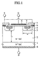
- Fig. 1 is a cross-sectional view showing a semiconductor device according to a first embodiment of the present invention.
- a semiconductor device according to the first embodiment is formed on a semiconductor substrate in which an N - -type drain region 2 is formed on a substrate region 1 made of N + -type silicon carbide of the 4H polytype, for example.
- a P-type base region 3 is disposed on an upper part of the drain region 2 including a principal surface of the drain region 2, which is opposite to a joint surface between the drain region 2 and the substrate region 1.
- An N + -type source region 4 is disposed above the base region 3 including the principal surface of the drain region 2.
- the semiconductor device according to the first embodiment constitutes a metal oxide semiconductor field effect transistor (MOSFET) which functions as a three-terminal switching element including the source, drain, and gate.
- MOSFET metal oxide semiconductor field effect transistor
- Fig. 1 shows a unit cell constituting the MOSFET.
- the unit cell includes two MOSFETs disposed to face each other while sandwiching the gate electrode 6.
- the actual semiconductor has a structure of arranging the unit cells shown in Fig. 1 adjacently to one another on the semiconductor substrate.
- the heterojunction semiconductor region 9 is disposed on the drain region 2 between the base regions 3 which respectively belong to the adjacent unit cells.
- the junction between the drain region 2 and the heterojunction semiconductor region 9 constitutes a heterojunction attributable to two materials having different band gaps, namely, silicon carbide and polycrystalline silicon. Accordingly, there is an energy barrier on an interface of the heterojunction.
- the heterojunction semiconductor region 9 is connected to the source electrode 7.
- the heterojunction semiconductor region 9 is made of the same material as the gate electrode 6. Therefore, the heterojunction semiconductor region 9 can be formed simultaneously with formation of the polycrystalline silicon layer constituting the gate electrode 6. In this way, the manufacturing process is simplified.
- a distance between the heterojunction semiconductor region 9 and the remotest position of the base region 3 from the heterojunction semiconductor region in the direction parallel to a principal surface of the semiconductor substrate i.e. the distance in the horizontal direction of Fig. 1 (such a distance will be hereinafter referred to as a horizontal distance w), is at least equal to or less than a thickness t of the drain region 2 immediately below the base region 3.
- the semiconductor device shown in Fig. 1 is supposed to be used as a power conversion element such as an inverter.
- the semiconductor device functions as a switching element in a forward direction operation and as a passive element in a reverse direction operation, respectively.
- the semiconductor device shown in Fig. 1 functions as the switching element.
- the semiconductor device shown in Fig. 1 functions as the passive element.
- the semiconductor device holds a cut-off state when the gate electrode 6 is set to the ground potential while grounding the source electrode 7 and applying a positive potential to the drain electrode 8.
- the semiconductor device holds a cut-off state when the gate electrode 6 is set to the ground potential while grounding the source electrode 7 and applying a positive potential to the drain electrode 8.
- an energy barrier against conduction electrons attributable to the pn-junction is formed between the source region 4 and the drain region 2 of the MOSFET by the base region 3.
- another energy barrier against the conduction electrons attributable to the heterojunction is formed between the heterojunction semiconductor region 9 and the drain region 2.
- the energy barrier in the heterojunction will be described later with reference to Fig. 2 to Fig. 6.
- the MOSFET functions as the switching element normally even if the heterojunction semiconductor region 9 is incorporated in the MOSFET.
- a reverse conduction current flows between the source electrode 7 and the drain electrode 8 through the heterojunction semiconductor region 9 when the gate electrode 6 and the source electrode 7 are set to ground potential while applying given negative potential to the drain electrode 8.
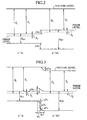
- Fig. 2 to Fig. 6 shows energy band structures of the semiconductor.
- the left side shows an energy band structure of the N - -type silicon corresponding to the heterojunction semiconductor region 9
- the right side shows an energy band structure of the N - -type silicon carbide of the 4H polytype corresponding to the drain region 2.
- the heterojunction semiconductor region 9 in Fig. 1 is made of polycrystalline silicon. However, in Fig. 2 to Fig. 6, description will be made by use of the energy band structure of silicon instead of polycrystalline silicon. To facilitate understandings of the characteristics of the heterojunction, description will be made on an energy level of an ideal semiconductor heterojunction where no interface level exists on a heterojunction interface.
- Fig. 2 is a view showing the energy band structures when the silicon and the silicon carbide do not contact each other.
- an electron affinity of the silicon is defined as ⁇ 1
- a work function thereof energy from a vacuum level to a Fermi level
- a Fermi energy thereof energy from a conduction band to the Fermi level
- a band gap thereof is defined as E G1
- an electron affinity of the silicon carbide is defined as ⁇ 2
- a work function thereof is defined as ⁇ 2
- a Fermi energy thereof is defined as ⁇ 2
- a band gap thereof is defined as E G2 .
- Fig. 3 is a view showing the energy band structures in which the heterojunction between the silicon and the silicon carbide is formed by allowing the silicon and the silicon carbide to contact each other. After allowing both of the silicon and the silicon carbide to contact each other, the energy barrier ⁇ E c remains to exist as similar to the state before the contact. Therefore, an electron accumulation layer having a width W1 is formed on the junction interface on the silicon side. On the contrary, a depletion layer having a width W2 is formed in the junction interface on the silicon carbide side.
- diffusion potential generated on the heterojunction interface is defined as V D
- V 1 diffusion potential component on the silicon side
- V 2 diffusion potential component on the silicon carbide side
- ⁇ 0 denotes a dielectric constant in vacuum
- ⁇ 2 denotes a relative dielectric constant of the silicon carbide
- N2 denotes an ionized impurity density of the silicon carbide.
- Fig. 4 to Fig. 6 shows the energy band structures in the junction interface between the heterojunction semiconductor region 9 and the drain region 2 shown in Fig. 1, which are based on the explanations of Fig. 2 and Fig. 3.
- Fig. 4 shows a state of thermal equilibrium where no voltage is applied to the source electrode 7 and the drain electrode 8.
- the energy band structure in the junction interface between the heterojunction semiconductor region 9 and the drain region 2 transits from the energy band structure in the cut-off state in the forward direction operation indicated by broken lines in Fig. 6 to the direction indicated by solid lines so as to offset the diffusion potential.
- An electron current flows from the drain region 2 toward the heterojunction semiconductor region 9 because there is virtually no energy barrier against the conduction electrons.
- a hole current hardly flows from the heterojunction semiconductor region 9 toward the drain region 2 because there is an energy barrier against holes.
- the heterojunction conductor region 9 is operated as a majority-carrier passive element. In this way, when the gate electrode 6 and the source electrode 7 are grounded and the given negative potential is applied to the drain electrode 8, a reverse conduction current flows between the source electrode 7 and the drain electrode 8 through the heterojunction semiconductor region 9.
- the heterojunction semiconductor region 9 When the heterojunction semiconductor region 9 is used as the passive element, it is possible to set the size of the energy barrier against the heterojunction semiconductor region 9, into a desired size by changing the conductivity type or the impurity density of the heterojunction semiconductor region 9. This is a characteristic not found in a Schottky junction, in which the size of the energy barrier is inherently determined by a work function of a metal material. For this reason, it is easy to achieve optimal design of the passive element in response to a withstand voltage system of the MOSFET as the switching element. Accordingly, it is possible to suppress the diffusion potential in the reverse conduction mode and to improve the degree of integration per unit area.
- a potential difference between the source electrode 7 and the drain electrode 8, i.e. an operating point of the passive element varies depending on the size of the reverse conduction current relative to the size of the formed passive element.
- the operation of the Schottky diode as the majority-carrier passive element in the reverse conduction mode is limited to 3 V or less at the maximum, which is equivalent to the diffusion potential of the pn-junction between the source electrode 7 and the drain electrode 8.
- the pn-junction between the base region and the drain region is operated when the potential difference between the source electrode 7 and the drain electrode 8 is equal to or above 3 V, and the hole current, which is a minority carrier, also starts flowing. Accordingly, it has been necessary to secure a given area for the Schottky diode so as to permit freewheeling of a given current at the potential difference at least equal to or below the diffusion potential of the pn-junction between the base region and the drain region.
- the horizontal distance w between the heterojunction semiconductor region 9 and the remotest position of the base region 3 from the heterojunction semiconductor region 9 is equal to or below the thickness t of the drain region 2 immediately below the base region 3.
- a PN diode is not operated immediately even when a potential difference greater than the diffusion potential of the pn-junction between the base region 3 and the drain region 2 is applied between the drain electrode 8 and the source electrode 7. The reason is as follows.
- the reverse conduction current When a given potential difference is applied between the drain electrode 8 and the source electrode 7, the reverse conduction current firstly flows through the heterojunction semiconductor region 9.
- the reverse conduction current in the drain region 2 flows from a junction with the heterojunction semiconductor region 9 toward a bottom part of the drain region 2 while spreading out in an angle of about 45°C. Accordingly, the reverse conduction current flows across the wide drain region 2 immediately below the base region 3.
- drain potential distribution occurs in the drain region 2 in response to the size of resistance and the size of the reverse conduction current. Therefore, part of the potential difference applied between the drain electrode 8 and the source electrode 7 is distributed in the drain region 2.
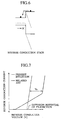
- the potential difference applied to the pn-junction between the base region 3 and the drain region 2 in the wide peripheral area of the base region becomes smaller than the potential difference applied between the drain electrode 8 and the source electrode 7 by just that much. Therefore, as shown in Fig. 7 as an example, even if the potential greater than the diffusion potential of the pn-junction between the base region 3 and the drain region 2 is applied between the drain electrode 8 and the source electrode 7, the PN diode is not operated immediately unlike a case in the related art.
- the heterojunction semiconductor region 9 continues to function as the majority-carrier passive element until application of a voltage which is higher by Va than the diffusion potential of the pn-junction.
- Fig. 8 is a calculation example showing a relation between a ratio of the horizontal distance w and the thickness t of the drain region 2 shown in Fig. 1, and the size of the voltage Va to top-up the diffusion potential of the pn-junction. As shown in Fig. 8, the voltage Va becomes larger as the ratio (distance w / thickness t) becomes smaller. In the semiconductor device shown in Fig.
- the top-up voltage Va becomes equal to about 0.4 V by setting the distance w to about 1 ⁇ m.
- the operation range for achieving the reverse conduction operation with the majority-carrier current is increased by the top-up voltage Va as compared to the related art. Accordingly, it is possible to increase the current density of the reverse conduction current flowing in the heterojunction semiconductor region 9 and thereby to reduce the area of the heterojunction semiconductor region 9. That is to say, it is possible provide a semiconductor device which functions as the switching element and the passive element, and permits higher integration at the same time.
- the base region 3 and the heterojunction semiconductor region 9 are arranged appropriately so that a freewheel current can flow at least from the heterojunction semiconductor region 9 to the drain region 2 in the vicinity of the remotest position of the base region 3 from the heterojunction semiconductor region 9 when the freewheel current flows from the source electrode 7 to the drain electrode 8 through the heterojunction semiconductor region 9. Accordingly, the operation range for achieving the reverse conduction operation with the majority-carrier current is increased. In this way, it is possible to increase the current density of the reverse conduction current flowing in the heterojunction semiconductor region 9 and thereby to improve the degree of integration.
- the operation range for achieving the reverse conduction current with the majority-carrier is further increased. In this way, it is possible to increase the current density of the reverse conduction current flowing in the heterojunction semiconductor region 9 further and thereby to improve the degree of integration further.
- Fig. 1 shows the MOSFET including the inversion-type channel
- the MOSFET may include an accumulation-type channel provided as an N-type region formed in a given region within the base region 3. That is to say, as shown in Fig. 10, for example, it is also possible to arrange an accumulative position 11 between the base region 3 and the insulating film 5.
- the semiconductor device includes the accumulative region (the accumulation-type channel) 11 as shown in Fig. 10, it is possible to conduct the semiconductor device at lower on resistance as compared to the semiconductor device including the inversion-type channel as shown in Fig. 1.
- a gate electrode 12 and a heterojunction semiconductor region 13 in Fig. 10 are made of P-type polycrystalline silicon. In this way, it is also possible to secure a shielding property. That is to say, when a semiconductor substrate constituting the drain region 2 is of the N-type, it is also possible to reduce the on-resistance by forming the gate electrode 12 and the heterojunction semiconductor region 13 as the P-type.
- the first embodiment has described the case of using the heterojunction semiconductor region 9 as the majority-carrier passive element.
- the present invention is not limited only to this configuration.
- a Schottky junction region 10 made of a given metal material for forming a Schottky junction with the drain region 2 instead of the heterojunction semiconductor region 9.
- the location for arranging the heterojunction semiconductor region 9 is not limited to the illustration in Fig. 1, and the location can be set freely.
- Fig. 12 it is possible to arrange the heterojunction semiconductor region 9 so as to be interposed between the mutually adjacent gate electrodes 6.
- the heterojunction semiconductor region 9 is arranged to abut on the drain region 2 while being interposed between the mutually adjacent base regions 3.
- a horizontal distance between the heterojunction semiconductor region 9 and the remotest position of the base region 3 from the heterojunction semiconductor region 9 is equivalent to a horizontal difference w from an end of the heterojunction semiconductor region 9 to the right end of the base region 3.
- the horizontal distance is equivalent to the end of the heterojunction semiconductor region 3 to the left end of the base region 3.
- heterojunction semiconductor regions 9a and 9b corresponding to the heterojunction semiconductor regions in the examples shown in Fig. 1 and in Fig. 12 at the same time. That is to say, it is possible to arrange the heterojunction semiconductor region 9b to be interposed between the mutually adjacent base regions 3, and to arrange the heterojunction semiconductor region 9a disposed outside the base region 3 at the same time. In this case, the base region 3 is sandwiched by both of the heterojunction semiconductor regions 9a and 9b. As shown in Fig.
- a horizontal distance between the heterojunction semiconductor region 9a or 9b and the remotest position of the base region 3 from the heterojunction semiconductor region 9a or 9b is equal to a half of a horizontal distance between both of the heterojunction semiconductor regions 9a and 9b.
- each of the horizontal distances is equal to a half of a distance between the left end of a portion where the heterojunction semiconductor region 9a on the outside abuts on the drain region 2 and the right end of a portion where the heterojunction semiconductor region 9b sandwiched by the two base regions 3 abuts on the drain region 2.
- each of the horizontal difference is equal to a half of the shortest horizontal difference between the portions where the two heterojunction semiconductor region 9a and 9b respectively abut on the drain region 2.
- the energy barrier against the conduction electrons is formed between the drain region 2 and the heterojunction semiconductor region 9 again, whereby the conduction electrons previously flowing between the drain region 2 and the heterojunction semiconductor region 9 are shielded by the energy barrier.
- the hole current hardly flows in the drain region 2. Accordingly, a reverse recovery current from the reverse conduction state to the cut-off state hardly flows, and a low-loss and high-speed reverse recovery switching operation is realized.
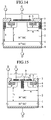
- Fig. 14 is a cross-sectional view corresponding to Fig. 1, which shows a semiconductor device according to a second embodiment of the present invention.
- description of the constituents performing the same operations as those in the semiconductor device shown in Fig. 1 will be omitted. Instead, differences from the semiconductor device shown in Fig. 1 will be described in detail.
- the heterojunction semiconductor region 9 is formed deeper than the base region 3. That is to say, a thickness k of the drain region 2 immediately below the heterojunction semiconductor region 9 is smaller than the thickness t of the drain region 2 immediately below the base region 3.
- Fig. 9 is an example of a calculation result showing a relation between a difference between the thickness t and the thickness k, and, the voltage Va.
- the voltage Va becomes larger as the difference in thickness (t-k) becomes larger.
- the voltage Va reaches an inflection point.
- the impurity density of the drain region 2 is set to about 1 ⁇ 10 16 cm -3 and the thickness thereof is set to about 10 ⁇ m while the impurity density of the base region 3 is set to about 1 ⁇ 10 18 cm -3 and the thickness thereof is set to about 1 ⁇ m.
- the depth of the heterojunction semiconductor region 9 is set deeper by about 1 ⁇ m than the depth of the base region 3.
- the horizontal distance w between the heterojunction semiconductor region 9 and the remotest position of the base region 3 from the heterojunction semiconductor position 9 is set to about 1 ⁇ m, for example. In this case, it is possible to obtain the top-up voltage Va of about 1.8 V. Accordingly, it is possible to obtain the effect several times higher than the semiconductor device of Fig. 1 in which the heterojunction semiconductor region 9 is formed only on the surface layer portion of the drain region 2.
- the range for causing the heterojunction semiconductor region 9 to function as the majority-carrier passive element is increased more than the semiconductor device of Fig. 1. In this way, it is possible to increase the current density of the reverse conduction current flowing in the heterojunction semiconductor region 9 further, and to reduce the area of the heterojunction semiconductor region 9 further.
- the second embodiment has described the case of using the heterojunction semiconductor region 9 as the majority-carrier passive element.
- the present invention is not limited only to this configuration.
- the Schottky junction region 10 made of a given metal material for forming the Schottky junction at the portion of the heterojunction semiconductor region 9. In this case as well, it is possible to obtain the above-described effect of the top-up voltage Va.
- the location for arranging the heterojunction semiconductor region 9 is not limited to the illustration in Fig. 14, and the location can be set freely.
- the horizontal distance between the heterojunction semiconductor region 9 and the remotest position of the base region 3 from the heterojunction semiconductor region 9 is equivalent to the horizontal difference w from the end of the heterojunction semiconductor region 9 to the right end of the base region 3.
- the horizontal distance is equivalent to the end of the heterojunction semiconductor region 3 to the heft end of the base region 3.
- the heterojunction semiconductor regions 9a and 9b corresponding to the heterojunction semiconductor regions in the examples shown in Fig. 14 and in Fig. 15 at the same time. That is to say, it is possible to arrange the heterojunction semiconductor region 9b to be interposed between the mutually adjacent base regions 3, and to arrange the heterojunction semiconductor region 9a disposed outside the base region 3 at the same time. In this case, the base region 3 is sandwiched by both of the heterojunction semiconductor regions 9a and 9b. As shown in Fig.
- the horizontal distance between the heterojunction semiconductor region 9a or 9b and the remotest position of the base region 3 from the heterojunction semiconductor region 9a or 9b is equal to a half of the horizontal distance between both of the heterojunction semiconductor regions 9a and 9b.
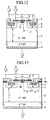
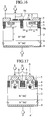
- Fig. 17 is a cross-sectional view showing a semiconductor device according to a third embodiment of the present invention.
- Fig. 17 is the cross-sectional view corresponding to Fig. 1 showing the first embodiment.
- Fig. 18 is a side view taken along the A-A' line in Fig. 17.
- description of the constituents performing the same operations as those in the semiconductor device shown in Fig. 1 will be omitted. Instead, differences from the semiconductor device shown in Fig. 1 will be described in detail.
- the semiconductor device according to the third embodiment has a trench-type MOSFET structure, in which trenches are formed on the surface layer portion of the drain region 2 and the insulating film 5 and the gate electrode 6 are formed inside each of the trenches. Moreover, the heterojunction semiconductor regions 9 are arranged at given intervals along the gate electrodes 6 so as to be interposed between the mutually adjacent gate electrodes 6. According to the semiconductor device shown in Fig. 17 and Fig. 18, it is possible to design the horizontal direction w between the heterojunction semiconductor region 9 and the remotest position of the base region 3 from the heterojunction semiconductor region 9 easily. In this way, it is possible to achieve a structure having the smaller distance w as compared to the semiconductor device shown in Fig. 1.
- the heterojunction semiconductor region 9 is formed almost as deep as the depth of the trench where the insulating film 5 and the gate electrode 6 are buried in.
- the present invention is not limited only to this configuration, and the depth of the heterojunction semiconductor region 9 is arbitrary. Nevertheless, by setting the depth of the heterojunction semiconductor region 9 as the same as the depth of the trench where the insulating film 5 and the gate electrode 6 are buried in, it is possible to carry out the step of forming the trench on the substrate and the step of forming the polycrystalline silicon layer as the gate electrode 6 and as the heterojunction semiconductor region 9 at the same time. In this way, the manufacturing process of this semiconductor device is simplified. Moreover, since the heterojunction semiconductor region 9 is formed deeper than the base region 3 as shown in Fig. 14, it is possible to obtain the higher top-up voltage Va.
- the heterojunction semiconductor regions 9 of the same shape are repeatedly arranged between the mutually adjacent cells.
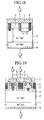
- Fig. 20 and Fig. 21 are cross-sectional views showing a semiconductor device according to a fourth embodiment of the present invention.
- Fig. 20 is the cross-sectional view corresponding to Fig. 1.
- Fig. 21 is a side view taken along the B-B' line in Fig. 20.
- description of the constituents performing the same operations as those in the semiconductor device shown in Fig. 1 will be omitted. Instead, differences from the semiconductor device shown in Fig. 1 will be described in detail.
- the semiconductor device includes a junction field effect transistor (JFET) as the switching element.
- JFET junction field effect transistor
- the semiconductor device uses a semiconductor substrate in which an N - -type drain region 22 is formed on a substrate region 21 made of N + -type silicon carbide of the 4H polytype, for example.
- a P-type base region 23 is disposed on an upper part of the drain region 22 including a principal surface of the drain region 22, which is opposite with a joint surface between the drain region 22 and the substrate region 21.
- An N + -type source region 24 is interposed between the mutually adjacent base regions 23.
- the base region 23 and the source region 24 are separated. However, the base region 23 and the source region 24 may contact each other.
- the base region 23 is connected to a gate electrode 26, the source region 24 is connected to a source electrode 27, and the drain region 22 is connected to a drain electrode 28, respectively.
- reference numeral 25 denotes an insulating film.
- heterojunction semiconductor regions 29 are arranged at given intervals along the base regions 23 so as to be interposed between the mutually adjacent base regions 23.
- the heterojunction semiconductor region 9 does not adversely affect an operation of the JFET as the switching element.
- the heterojunction semiconductor region 29 has similar operation and effect as those of the semiconductor device shown in Fig. 1. Since the JFET is used as the switching element, there is a problem in light of improvement in the shielding property between the source region 24 and the drain region 22. However, it is possible to improve the shielding property by locating the heterojunction semiconductor region 9 in a given position.
- the present invention is not limited only to this configuration. It is possible to use any type of semiconductor materials as the substrate material, such as silicon, silicon-germanium, gallium nitride or diamond. Although the embodiments have been described on the semiconductor devices applying the silicon carbide of the 4H polytype, it is possible to use silicon carbide of any other type such as the 6H polytype or the 3C polytype.
- Each of the embodiments has shown the transistor of a so-called vertical structure configured to flow the drain current in the vertical direction, in which the drain electrode 8 or 28 and the source electrode 7 or 27 are disposed so as to face each other while sandwiching the drain region 2 or 22.
- the present invention is not limited only to this structure.
- the present invention is not limited only to this configuration. It is possible to use any material as long as such a material can form a heterojunction with silicon carbide.
- the present invention is not limited only to this configuration. It is also possible to adopt any other combinations such as a combination of N-type silicon carbide and P-type polycrystalline silicon, a combination of P-type silicon carbide and P-type polycrystalline silicon, or P-type silicon carbide and N-type polycrystalline silicon.
- the switching element is configured as the MOSFET or the JFET.
- other switching elements such as a bipolar transistor.
- the size of the energy barrier against the conduction electrons which is formed between the drain region and the heterojunction semiconductor region, into a desired size by changing the conductivity type or the impurity density of the heterojunction semiconductor region.
- This is the characteristic not found in the Schottky junction, in which the size of the energy barrier is inherently determined by the work function of the metal material.
- it is easy to achieve optimal design of the passive element in response to a withstand voltage system of the MOSFET as the switching element. Accordingly, it is possible to suppress the diffusion potential in the reverse conduction mode and to improve the degree of integration per unit area. As a result, it is possible to reduce the size of the elements and to simplify the manufacturing processes thereof.
Landscapes
- Insulated Gate Type Field-Effect Transistor (AREA)
- Junction Field-Effect Transistors (AREA)
- Electrodes Of Semiconductors (AREA)
Applications Claiming Priority (2)
| Application Number | Priority Date | Filing Date | Title |
|---|---|---|---|
| JP2003420383A JP4066946B2 (ja) | 2003-12-18 | 2003-12-18 | 半導体装置 |
| JP2003420383 | 2003-12-18 |
Publications (3)
| Publication Number | Publication Date |
|---|---|
| EP1544920A2 true EP1544920A2 (de) | 2005-06-22 |
| EP1544920A3 EP1544920A3 (de) | 2010-06-02 |
| EP1544920B1 EP1544920B1 (de) | 2014-05-07 |
Family
ID=34510655
Family Applications (1)
| Application Number | Title | Priority Date | Filing Date |
|---|---|---|---|
| EP04029475.3A Expired - Lifetime EP1544920B1 (de) | 2003-12-18 | 2004-12-13 | Halbleiteranordnung mit einem Heteroübergang oder einem Schottky-Übergang |
Country Status (3)
| Country | Link |
|---|---|
| US (1) | US7151280B2 (de) |
| EP (1) | EP1544920B1 (de) |
| JP (1) | JP4066946B2 (de) |
Cited By (9)
| Publication number | Priority date | Publication date | Assignee | Title |
|---|---|---|---|---|
| EP1863096A1 (de) * | 2006-05-30 | 2007-12-05 | Nissan Motor Company Limited | Halbleiteranordnung und Verfahren zu deren Herstellung |
| US7521731B2 (en) | 2004-12-02 | 2009-04-21 | Nissan Motor Co., Ltd. | Semiconductor device and method of manufacturing the same |
| CN103493208A (zh) * | 2011-04-19 | 2014-01-01 | 日产自动车株式会社 | 半导体装置及其制造方法 |
| CN104620381A (zh) * | 2012-09-06 | 2015-05-13 | 三菱电机株式会社 | 半导体装置 |
| EP3223316A1 (de) * | 2016-03-24 | 2017-09-27 | ABB Technology AG | Leistungshalbleiterbauelement mit breiter bandbreite und verfahren zur herstellung solch eines bauelements |
| WO2019101685A1 (de) * | 2017-11-23 | 2019-05-31 | Robert Bosch Gmbh | Vertikaler leistungstransistor mit heteroübergangen |
| CN110379860A (zh) * | 2019-07-12 | 2019-10-25 | 中国科学院合肥物质科学研究院 | 一种实现电极化整流效应的方法 |
| WO2020221517A1 (de) * | 2019-04-30 | 2020-11-05 | Robert Bosch Gmbh | Halbleiterbauelement und verfahren zur herstellung eines halbleiterbauelements |
| CN114664929A (zh) * | 2022-04-21 | 2022-06-24 | 电子科技大学 | 一种集成异质结二极管的分离栅SiC MOSFET及其制作方法 |
Families Citing this family (27)
| Publication number | Priority date | Publication date | Assignee | Title |
|---|---|---|---|---|
| JP4039376B2 (ja) * | 2004-03-09 | 2008-01-30 | 日産自動車株式会社 | 半導体装置 |
| JP5087818B2 (ja) * | 2005-03-25 | 2012-12-05 | 日亜化学工業株式会社 | 電界効果トランジスタ |
| JP4935075B2 (ja) * | 2006-01-05 | 2012-05-23 | 住友電気工業株式会社 | 電極一体形成型窒化物系半導体装置 |
| US7714352B2 (en) * | 2006-02-09 | 2010-05-11 | Nissan Motor Co., Ltd. | Hetero junction semiconductor device |
| JP5061473B2 (ja) * | 2006-02-24 | 2012-10-31 | 住友電気工業株式会社 | 窒化物系半導体装置 |
| JP4900662B2 (ja) * | 2006-03-02 | 2012-03-21 | 独立行政法人産業技術総合研究所 | ショットキーダイオードを内蔵した炭化ケイ素mos電界効果トランジスタおよびその製造方法 |
| EP1850396A3 (de) * | 2006-04-28 | 2008-09-17 | Nissan Motor Co., Ltd. | Halbleiterbauelement und dessen Herstellungsmethode |
| JP5233173B2 (ja) * | 2007-06-08 | 2013-07-10 | 日産自動車株式会社 | 半導体装置の製造方法 |
| US8188484B2 (en) * | 2008-12-25 | 2012-05-29 | Rohm Co., Ltd. | Semiconductor device |
| US8188538B2 (en) | 2008-12-25 | 2012-05-29 | Rohm Co., Ltd. | Semiconductor device and method of manufacturing semiconductor device |
| JP2014241426A (ja) * | 2008-12-25 | 2014-12-25 | ローム株式会社 | 半導体装置 |
| JP2011134910A (ja) | 2009-12-24 | 2011-07-07 | Rohm Co Ltd | SiC電界効果トランジスタ |
| US9461124B2 (en) * | 2011-09-08 | 2016-10-04 | Tamura Corporation | Ga2O3 semiconductor element |
| CN103782392A (zh) | 2011-09-08 | 2014-05-07 | 株式会社田村制作所 | Ga2O3 系半导体元件 |
| JP6024117B2 (ja) * | 2012-02-20 | 2016-11-09 | 日産自動車株式会社 | 半導体装置の製造方法 |
| JP5992094B2 (ja) * | 2013-04-03 | 2016-09-14 | 三菱電機株式会社 | 半導体装置 |
| WO2014203317A1 (ja) * | 2013-06-17 | 2014-12-24 | 株式会社日立製作所 | 半導体装置およびその製造方法、並びに電力変換装置 |
| US9214572B2 (en) * | 2013-09-20 | 2015-12-15 | Monolith Semiconductor Inc. | High voltage MOSFET devices and methods of making the devices |
| US10483389B2 (en) * | 2014-07-02 | 2019-11-19 | Hestia Power Inc. | Silicon carbide semiconductor device |
| US10418476B2 (en) | 2014-07-02 | 2019-09-17 | Hestia Power Inc. | Silicon carbide semiconductor device |
| JP6168370B2 (ja) * | 2015-12-17 | 2017-07-26 | ローム株式会社 | SiC電界効果トランジスタ |
| JP6649183B2 (ja) | 2016-05-30 | 2020-02-19 | 株式会社東芝 | 半導体装置 |
| US10937901B2 (en) * | 2018-03-14 | 2021-03-02 | Fuji Electric Co., Ltd. | Insulated gate semiconductor device with injuction supression structure and method of manufacturing same |
| JP7843145B2 (ja) * | 2022-01-19 | 2026-04-09 | 日産自動車株式会社 | 半導体装置及びその製造方法 |
| CN116598340B (zh) * | 2023-07-10 | 2023-09-22 | 苏州锴威特半导体股份有限公司 | 一种SiC MOSFET及其制作工艺方法 |
| CN117497601B (zh) * | 2023-12-28 | 2024-05-07 | 深圳天狼芯半导体有限公司 | 平面型碳化硅晶体管的结构、制造方法及电子设备 |
| CN117690970A (zh) * | 2024-02-04 | 2024-03-12 | 深圳天狼芯半导体有限公司 | 一种碳化硅功率器件及其制作方法 |
Family Cites Families (9)
| Publication number | Priority date | Publication date | Assignee | Title |
|---|---|---|---|---|
| JPH02100367A (ja) * | 1988-10-07 | 1990-04-12 | Nissan Motor Co Ltd | 縦型伝導度変調型mosfet |
| SE9404452D0 (sv) * | 1994-12-22 | 1994-12-22 | Abb Research Ltd | Semiconductor device having an insulated gate |
| JPH09102602A (ja) * | 1995-10-05 | 1997-04-15 | Nippon Telegr & Teleph Corp <Ntt> | Mosfet |
| US7126169B2 (en) * | 2000-10-23 | 2006-10-24 | Matsushita Electric Industrial Co., Ltd. | Semiconductor element |
| JP4197400B2 (ja) * | 2001-03-29 | 2008-12-17 | 三菱電機株式会社 | 炭化珪素半導体からなる半導体装置 |
| JP3620513B2 (ja) * | 2002-04-26 | 2005-02-16 | 日産自動車株式会社 | 炭化珪素半導体装置 |
| US7217950B2 (en) * | 2002-10-11 | 2007-05-15 | Nissan Motor Co., Ltd. | Insulated gate tunnel-injection device having heterojunction and method for manufacturing the same |
| US7138668B2 (en) * | 2003-07-30 | 2006-11-21 | Nissan Motor Co., Ltd. | Heterojunction diode with reduced leakage current |
| EP1519419B1 (de) * | 2003-09-24 | 2018-02-21 | Nissan Motor Co., Ltd. | Halbleitervorrichtung und Verfahren zu deren Herstellung |
-
2003
- 2003-12-18 JP JP2003420383A patent/JP4066946B2/ja not_active Expired - Lifetime
-
2004
- 2004-12-13 EP EP04029475.3A patent/EP1544920B1/de not_active Expired - Lifetime
- 2004-12-16 US US11/012,205 patent/US7151280B2/en not_active Expired - Lifetime
Non-Patent Citations (1)
| Title |
|---|
| None |
Cited By (13)
| Publication number | Priority date | Publication date | Assignee | Title |
|---|---|---|---|---|
| US7521731B2 (en) | 2004-12-02 | 2009-04-21 | Nissan Motor Co., Ltd. | Semiconductor device and method of manufacturing the same |
| EP1863096A1 (de) * | 2006-05-30 | 2007-12-05 | Nissan Motor Company Limited | Halbleiteranordnung und Verfahren zu deren Herstellung |
| CN103493208B (zh) * | 2011-04-19 | 2017-03-22 | 日产自动车株式会社 | 半导体装置及其制造方法 |
| EP2701201A4 (de) * | 2011-04-19 | 2015-04-22 | Nissan Motor | Halbleitervorrichtung und herstellungsverfahren dafür |
| US9252261B2 (en) | 2011-04-19 | 2016-02-02 | Nissan Motor Co., Ltd. | Semiconductor device and manufacturing method of the same |
| CN103493208A (zh) * | 2011-04-19 | 2014-01-01 | 日产自动车株式会社 | 半导体装置及其制造方法 |
| CN104620381A (zh) * | 2012-09-06 | 2015-05-13 | 三菱电机株式会社 | 半导体装置 |
| CN104620381B (zh) * | 2012-09-06 | 2017-04-19 | 三菱电机株式会社 | 半导体装置 |
| EP3223316A1 (de) * | 2016-03-24 | 2017-09-27 | ABB Technology AG | Leistungshalbleiterbauelement mit breiter bandbreite und verfahren zur herstellung solch eines bauelements |
| WO2019101685A1 (de) * | 2017-11-23 | 2019-05-31 | Robert Bosch Gmbh | Vertikaler leistungstransistor mit heteroübergangen |
| WO2020221517A1 (de) * | 2019-04-30 | 2020-11-05 | Robert Bosch Gmbh | Halbleiterbauelement und verfahren zur herstellung eines halbleiterbauelements |
| CN110379860A (zh) * | 2019-07-12 | 2019-10-25 | 中国科学院合肥物质科学研究院 | 一种实现电极化整流效应的方法 |
| CN114664929A (zh) * | 2022-04-21 | 2022-06-24 | 电子科技大学 | 一种集成异质结二极管的分离栅SiC MOSFET及其制作方法 |
Also Published As
| Publication number | Publication date |
|---|---|
| JP2005183563A (ja) | 2005-07-07 |
| EP1544920A3 (de) | 2010-06-02 |
| EP1544920B1 (de) | 2014-05-07 |
| US7151280B2 (en) | 2006-12-19 |
| US20050133794A1 (en) | 2005-06-23 |
| JP4066946B2 (ja) | 2008-03-26 |
Similar Documents
| Publication | Publication Date | Title |
|---|---|---|
| US7151280B2 (en) | Semiconductor device | |
| JP5011681B2 (ja) | 半導体装置 | |
| US20210175348A1 (en) | Lateral Transistors and Methods with Low-Voltage-Drop Shunt to Body Diode | |
| EP1587147A2 (de) | Halbleiteranordnung mit Heteroübergang | |
| US7005704B2 (en) | Insulated gate drive semiconductor device | |
| US20080035992A1 (en) | Semiconductor device | |
| WO2008156674A1 (en) | Improved power switching transistors | |
| WO2017047286A1 (ja) | 半導体装置 | |
| US6809354B2 (en) | Semiconductor device | |
| JP4039376B2 (ja) | 半導体装置 | |
| CN111384174A (zh) | 沟槽型mos场效应晶体管及方法、电子设备 | |
| CN113410284A (zh) | 碳化硅半导体结构和碳化硅半导体器件 | |
| CN114175266A (zh) | 功率晶体管单元与功率晶体管 | |
| JP4742539B2 (ja) | 半導体装置 | |
| JP3319228B2 (ja) | たて型半導体素子およびその製造方法 | |
| JP4131193B2 (ja) | 半導体装置 | |
| CN116895682A (zh) | 垂直屏蔽栅极累积场效应晶体管 | |
| JP3975992B2 (ja) | 半導体装置及びその製造方法 | |
| JP2006165013A (ja) | 半導体装置及びその製造方法 | |
| CN100561739C (zh) | 半导体装置 | |
| US9276135B2 (en) | Junction field effect transistor with vertical PN junction | |
| JPH09246545A (ja) | 電力用半導体素子 | |
| JP3945368B2 (ja) | 炭化珪素半導体装置 | |
| JP2006093545A (ja) | 半導体装置 | |
| US20250056869A1 (en) | Wide band gap semiconductor device |
Legal Events
| Date | Code | Title | Description |
|---|---|---|---|
| PUAI | Public reference made under article 153(3) epc to a published international application that has entered the european phase |
Free format text: ORIGINAL CODE: 0009012 |
|
| 17P | Request for examination filed |
Effective date: 20041213 |
|
| AK | Designated contracting states |
Kind code of ref document: A2 Designated state(s): AT BE BG CH CY CZ DE DK EE ES FI FR GB GR HU IE IS IT LI LT LU MC NL PL PT RO SE SI SK TR |
|
| AX | Request for extension of the european patent |
Extension state: AL BA HR LV MK YU |
|
| PUAL | Search report despatched |
Free format text: ORIGINAL CODE: 0009013 |
|
| AK | Designated contracting states |
Kind code of ref document: A3 Designated state(s): AT BE BG CH CY CZ DE DK EE ES FI FR GB GR HU IE IS IT LI LT LU MC NL PL PT RO SE SI SK TR |
|
| AX | Request for extension of the european patent |
Extension state: AL BA HR LV MK YU |
|
| AKX | Designation fees paid |
Designated state(s): DE FR GB |
|
| 17Q | First examination report despatched |
Effective date: 20110329 |
|
| GRAP | Despatch of communication of intention to grant a patent |
Free format text: ORIGINAL CODE: EPIDOSNIGR1 |
|
| INTG | Intention to grant announced |
Effective date: 20140129 |
|
| GRAS | Grant fee paid |
Free format text: ORIGINAL CODE: EPIDOSNIGR3 |
|
| GRAA | (expected) grant |
Free format text: ORIGINAL CODE: 0009210 |
|
| AK | Designated contracting states |
Kind code of ref document: B1 Designated state(s): DE FR GB |
|
| REG | Reference to a national code |
Ref country code: GB Ref legal event code: FG4D |
|
| REG | Reference to a national code |
Ref country code: DE Ref legal event code: R096 Ref document number: 602004045010 Country of ref document: DE Effective date: 20140612 |
|
| REG | Reference to a national code |
Ref country code: DE Ref legal event code: R097 Ref document number: 602004045010 Country of ref document: DE |
|
| PLBE | No opposition filed within time limit |
Free format text: ORIGINAL CODE: 0009261 |
|
| STAA | Information on the status of an ep patent application or granted ep patent |
Free format text: STATUS: NO OPPOSITION FILED WITHIN TIME LIMIT |
|
| 26N | No opposition filed |
Effective date: 20150210 |
|
| REG | Reference to a national code |
Ref country code: DE Ref legal event code: R097 Ref document number: 602004045010 Country of ref document: DE Effective date: 20150210 |
|
| REG | Reference to a national code |
Ref country code: FR Ref legal event code: PLFP Year of fee payment: 12 |
|
| REG | Reference to a national code |
Ref country code: FR Ref legal event code: PLFP Year of fee payment: 13 |
|
| REG | Reference to a national code |
Ref country code: FR Ref legal event code: PLFP Year of fee payment: 14 |
|
| PGFP | Annual fee paid to national office [announced via postgrant information from national office to epo] |
Ref country code: GB Payment date: 20231124 Year of fee payment: 20 |
|
| PGFP | Annual fee paid to national office [announced via postgrant information from national office to epo] |
Ref country code: FR Payment date: 20231122 Year of fee payment: 20 Ref country code: DE Payment date: 20231121 Year of fee payment: 20 |
|
| REG | Reference to a national code |
Ref country code: DE Ref legal event code: R079 Ref document number: 602004045010 Country of ref document: DE Free format text: PREVIOUS MAIN CLASS: H01L0029780000 Ipc: H10D0030600000 |
|
| REG | Reference to a national code |
Ref country code: DE Ref legal event code: R071 Ref document number: 602004045010 Country of ref document: DE |
|
| REG | Reference to a national code |
Ref country code: GB Ref legal event code: PE20 Expiry date: 20241212 |
|
| PG25 | Lapsed in a contracting state [announced via postgrant information from national office to epo] |
Ref country code: GB Free format text: LAPSE BECAUSE OF EXPIRATION OF PROTECTION Effective date: 20241212 |
|
| PG25 | Lapsed in a contracting state [announced via postgrant information from national office to epo] |
Ref country code: GB Free format text: LAPSE BECAUSE OF EXPIRATION OF PROTECTION Effective date: 20241212 |