EP1526720A2 - Caméra numérique avec dispositifs d'affichage interchangeables - Google Patents
Caméra numérique avec dispositifs d'affichage interchangeables Download PDFInfo
- Publication number
- EP1526720A2 EP1526720A2 EP05000883A EP05000883A EP1526720A2 EP 1526720 A2 EP1526720 A2 EP 1526720A2 EP 05000883 A EP05000883 A EP 05000883A EP 05000883 A EP05000883 A EP 05000883A EP 1526720 A2 EP1526720 A2 EP 1526720A2
- Authority
- EP
- European Patent Office
- Prior art keywords
- image
- circuit
- processing circuit
- operable
- output
- Prior art date
- Legal status (The legal status is an assumption and is not a legal conclusion. Google has not performed a legal analysis and makes no representation as to the accuracy of the status listed.)
- Withdrawn
Links
Images


Classifications
-
- H—ELECTRICITY
- H04—ELECTRIC COMMUNICATION TECHNIQUE
- H04N—PICTORIAL COMMUNICATION, e.g. TELEVISION
- H04N23/00—Cameras or camera modules comprising electronic image sensors; Control thereof
- H04N23/80—Camera processing pipelines; Components thereof
- H04N23/84—Camera processing pipelines; Components thereof for processing colour signals
- H04N23/843—Demosaicing, e.g. interpolating colour pixel values
-
- H—ELECTRICITY
- H04—ELECTRIC COMMUNICATION TECHNIQUE
- H04N—PICTORIAL COMMUNICATION, e.g. TELEVISION
- H04N23/00—Cameras or camera modules comprising electronic image sensors; Control thereof
- H04N23/60—Control of cameras or camera modules
- H04N23/63—Control of cameras or camera modules by using electronic viewfinders
-
- H—ELECTRICITY
- H04—ELECTRIC COMMUNICATION TECHNIQUE
- H04N—PICTORIAL COMMUNICATION, e.g. TELEVISION
- H04N2201/00—Indexing scheme relating to scanning, transmission or reproduction of documents or the like, and to details thereof
- H04N2201/0008—Connection or combination of a still picture apparatus with another apparatus
- H04N2201/0034—Details of the connection, e.g. connector, interface
- H04N2201/0048—Type of connection
- H04N2201/0049—By wire, cable or the like
-
- H—ELECTRICITY
- H04—ELECTRIC COMMUNICATION TECHNIQUE
- H04N—PICTORIAL COMMUNICATION, e.g. TELEVISION
- H04N2201/00—Indexing scheme relating to scanning, transmission or reproduction of documents or the like, and to details thereof
- H04N2201/0077—Types of the still picture apparatus
- H04N2201/0089—Image display device
-
- H—ELECTRICITY
- H04—ELECTRIC COMMUNICATION TECHNIQUE
- H04N—PICTORIAL COMMUNICATION, e.g. TELEVISION
- H04N23/00—Cameras or camera modules comprising electronic image sensors; Control thereof
- H04N23/80—Camera processing pipelines; Components thereof
- H04N23/82—Camera processing pipelines; Components thereof for controlling camera response irrespective of the scene brightness, e.g. gamma correction
-
- H—ELECTRICITY
- H04—ELECTRIC COMMUNICATION TECHNIQUE
- H04N—PICTORIAL COMMUNICATION, e.g. TELEVISION
- H04N25/00—Circuitry of solid-state image sensors [SSIS]; Control thereof
- H04N25/10—Circuitry of solid-state image sensors [SSIS]; Control thereof for transforming different wavelengths into image signals
- H04N25/11—Arrangement of colour filter arrays [CFA]; Filter mosaics
- H04N25/13—Arrangement of colour filter arrays [CFA]; Filter mosaics characterised by the spectral characteristics of the filter elements
- H04N25/135—Arrangement of colour filter arrays [CFA]; Filter mosaics characterised by the spectral characteristics of the filter elements based on four or more different wavelength filter elements
- H04N25/136—Arrangement of colour filter arrays [CFA]; Filter mosaics characterised by the spectral characteristics of the filter elements based on four or more different wavelength filter elements using complementary colours
Definitions
- the present invention relates to a device for interchanging displays in a digital camera, and more precisely to a device for interchanging displays in a digital camera whereby the method of display changes between displaying the image with a built-in liquid crystal device and displaying it on a monitor device by linking the camera to the monitor device with the help of a video cable, and between when focusing and not focusing.
- Some digital cameras in addition to having a small liquid crystal or other display device, have an image output terminal whereby image signals are fed to an external monitor device.
- image signals are fed to an external monitor device.
- the screen is relatively small and it does not detract very much from the quality of the image even if it is displayed using an image signal which has been processed so as to cull a large number of pixels. However, this is not so if an image signal of this sort is used to display the image on a monitor device with a large screen.
- the situation is that especially where the image is processed by means of a microprocessor, it is possible to shorten the time required for processing in direct proportion to the number of pixels that are culled.
- an embodiment of the present invention provides a digital camera with interchangeable displays wherein large numbers of pixels are culled in processing the image signal which is output for display on the display device which is built into the camera, while a smaller number are culled in processing the image signal which is output for display on an external monitor device using a video cable.
- another embodiment provides a digital camera with interchangeable displays wherein contrast is emphasised in processing the image signal which is output for display on the display device which is built into the camera, while reproduction of tone is emphasised in processing the image signal which is output for display on an external monitor device using a video cable.
- a further embodiment provides a digital camera with interchangeable displays wherein during adjustment of the focus an image signal is output which is processed in such a manner that part of the image is enlarged.
- a digital camera has a built-in display device and an image output terminal which transmits image signals to an external monitor device, and comprises means for changing the position of the focus, means for detecting the position of the focus, means for detecting whether or not the video cable has been inserted, means for changing the method of processing employed in the means for processing the image, and a method of feeding the output of the means for processing the image to the image output terminal.
- the above configuration permits the realisation of a digital camera with interchangeable displays wherein large numbers of pixels are culled and the image signal is processed at high speed when it is being output for display on the display device which is built into the camera, while a smaller number of pixels are culled with higher image quality when processing the image signal which is output for display on an external monitor device using a video cable.
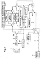
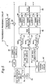
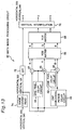
- Fig. 1 is a block diagram illustrating the first embodiment of the digital camera with interchangeable displays to which the present invention pertains, and depicts a device for changing the display mode by inserting or removing the video cable.
- the image is displayed with rough picture quality at a higher number of frames per second (eg 6 frames / sec) on the display device of the camera itself, but at a lower number of frames per second (eg 4 frames / sec) and finer picture quality when the video cable is inserted and the image displayed on a television or other external monitor device 28.
- means for capturing an image is composed of a lens 2 and a charge-coupled device (CCD) 4.
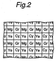
- the CCD 4 has on its surface for the purpose of colouration, for instance, a colour filter of the type illustrated in Fig. 2.
- 6 is an A/D converter
- 8 is a progressive processing circuit which processes image signals without culling of pixel signals
- 10 is a first processing circuit which culls large numbers of pixel signals
- 12 is a second processing circuit which culls fewer pixel signals
- 14 is a detector which detects whether the video cable has been inserted or not
- 16 is the shutter button of the digital camera
- 18 is a flip-flop
- 20 is a CCD drive circuit
- 22 is a D/A converter
- 24 is a bit map memory which memorises the image which has been captured
- 26 is the display device which is located on the body of the camera and is preferably a liquid crystal display
- 28 is a television or other display device
- 30 is the video cable which connects the display device 28 to
- a low-level signal is output from the Q output of the flip-flop 18, as a result of which the CCD drive circuit 20 counts the adjoining pixels of the CCD 4. For example, it counts the magenta (Mg) and yellow (Ye) pixels above and below, and the green (G) and cyan (C) pixels above and below, outputting simplified image data in PD Mix mode, so to speak.
- the low-level signal from the Q output also causes the first interlocking switches S1a and S1b to be set in the positions denoted by the unbroken lines, while also causing the switch S3 to assume the position denoted by the unbroken line.
- action differs between when the video cable 30 is removed and the switch S4 is in the position denoted by the unbroken line (main body display mode), and when the video cable 30 is inserted and the switch S4 is in the position denoted by the broken line (monitor display mode).
- the video cable 30 is removed, and the detector 14 for detecting whether the video cable has been inserted or not detects this state. When it does so, it outputs a first signal (eg a high-level signal), and the interlocking switches S2a and S2b are set in the positions denoted by the unbroken lines. Consequently, the PDMix mode image signal obtained from the CCD 4 is fed by way of the A/D converter 6, the first processing circuit 10 and the D/A converter 22 to the liquid crystal display 26 on the main body of the camera. As will be explained later, the first processing circuit 10 culls large numbers of pixel signals while processing the image, and so it is able to construct the image very quickly (eg at 6 frames / sec).
- a first signal eg a high-level signal
- the video cable 30 is inserted, and the detector 14 for detecting whether the video cable has been inserted or not detects this state. When it does so, it outputs a second signal (eg a low-level signal), and the interlocking switches S2a and S2b are set in the positions denoted by the broken lines. Consequently, the PDMix mode image signal obtained from the CCD 4 is fed by way of the A/D converter 6, the second processing circuit 12 and the D/A converter 22 to the monitor display device 28. As will be explained later, the second processing circuit 12 culls a relatively small number of pixel signals while processing the image, and so while it constructs the image slowly (eg at 4 frames / sec), the completed image is sharper than in the case of main body display mode.
- a second signal eg a low-level signal
- the shutter button 16 If the shutter button 16 is depressed, a set signal is input into the S input of the flip-flop 18, and a high-level signal is output from the Q output of the same, as a result of which the CCD drive circuit 20 is set in progressive mode wherein it outputs all the pixels of the CCD 4 without modification.
- the high-level signal from the Q output also causes the first interlocking switches S1a and S1b to be set in the positions denoted by the broken lines, as also the switch 3.
- This means that the progressive mode video signal obtained from the CCD 4 is fed by way of the AID converter 6, the progressive processing circuit 8 and the D/A converter 22 to the memory 24.
- the progressive processing circuit 8 one frame of image data is processed progressively and fed as bit map data to the memory 24.
- the progressive processing circuit 8 When the progressive processing of one frame of image data is complete and all the pixel signals are memorised in the bit map memory 24, the progressive processing circuit 8 inputs a re-set signal into the R input of the flip-flop 18, and a low-level signal is output from the Q output of the same. As a result of this low-level signal, the CCD drive circuit 20 is set again in PDMix mode. Also as a result of the low-level signal from the Q output, the first interlocking switches S1a and S1b are set in the positions denoted by the unbroken lines, and the switch S3 is returned to the position denoted in the same manner.
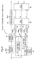
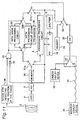
- Fig. 3 is a block diagram illustrating the first image processing circuit 10 depicted in Fig. 1.
- 32 is a horizontal sampling circuit
- 34 is a gamma correction circuit
- 36 is an over-sampling circuit
- 38 is a one pixel delay circuit
- 40 is a one horizontal period delay circuit
- 42 is a one pixel delay circuit
- 44 is a subtracter
- 46 is an adder
- 48 is a subtracter
- 50, 52 and 54 are each samplehold circuits
- 56 is an RGB matrix
- 58 is a YUV matrix.
- the horizontal sampling circuit 32 samples the brightness signal Y with a 3 MHz clock. If pixel signals are being fed at 12 MHz, this means that one pixel in four is sampled, If there are 640 pixels in one horizontal period, 160 pixels are sampled. The degree of culling is determined by this horizontal sampling circuit 32. Here it is a relatively large cull. Culled brightness signals pass through the gamma correction device 34 and are converted to 6 MHz in the over-sampling circuit 36. The same rate of Y output is obtained as with the second processing circuit illustrated in Fig. 4 and described below.
- the sample-hold circuits 50, 52 and 54 sample and hold R-Y, Y and B-Y signals respectively with 5 MHz clocks.
- the R-Y, Y and B-Y signals are sampled and held, while R, G and B signals are constructed by the RGB matrix 56, together with U and V signals by the YUV matrix.
- the first processing circuit 10 illustrated in Fig. 3 has a smaller number of gamma-corrected Y signals, while gamma correction of the LPF circuit in the circuit which processes colour signals and the R, G and B colour signals is omitted. This allows high-speed processing, and images are generated at 6 frames / sec, for instance.
- the first processing circuit illustrated in Fig. 3 is the circuit which operates during main body display mode, and generates six frames per second. As a result, it is possible to speed up the renewal rate of the liquid crystal display device 26 on the main body.
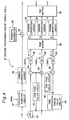
- Fig. 4 is a block diagram illustrating the second image processing circuit 12 depicted in Fig. 1. It differs from the first processing circuit illustrated in Fig. 3 in that the sampling frequency of horizontal sampling circuit 32' is 6 MHz, while it also has a low-pass filter 60, a pedestal generator 62, an adder 64, and gamma correction circuits 66, 68 and 70. In all other respects it is configured in the same manner as depicted in Fig. 3, and a description will be omitted.
- the horizontal sampling circuit 32' samples the brightness signal Y with a 6 MHz clock.
- the degree of culling is smaller than in the case of the horizontal sampling circuit 32, and images are generated at the rate of four frames per second. Since the degree of culling is small, it is possible to construct a fine-grained image even on a large monitor screen.
- a low-pass filter 60 on the circuit which processes colour makes it possible to suppress untrue colours at points where the brightness changes.
- Fig. 5 is a block diagram illustrating a progressive processing circuit 8. This differs from the second processing circuit 12 illustrated in Fig. 4 in that the circuit which processes the brightness signal has a low-pass filter 72 in place of the horizontal sampling circuit 32', while the circuit which processes colour has in addition a horizontal period delay circuit 74 and an adder 76. Moreover, the delay circuit provided on the circuit which processes the B-Y signal is not the one horizontal period delay circuit 40 but the two horizontal periods delay circuit 40', and the sampling frequency of the sample-hold circuits 50', 52' and 54' is 3 MHz.
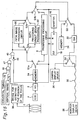
- Fig. 6 is a block diagram illustrating the second embodiment of the digital camera with interchangeable displays to which the present invention pertains.
- a third processing circuit 80 makes it possible to display an image which has been processed with emphasis on contrast in such a manner as to be easy to view outdoors on the display device 26 of the camera itself
- a fourth processing circuit 82 makes it possible to display an image which has been processed with emphasis on reproduction of tone in such a manner as to be easy to view when the video cable is inserted and the image is displayed on a television or other external monitor device 28.
- Fig. 6 80 is the third processing circuit whereby the image is processed with emphasis on contrast, and 82 is the fourth processing circuit whereby it is processed with emphasis on reproduction of tone.
- action differs between when the video cable 30 is removed and the switch S4 is in the position denoted by the unbroken line (main body display mode), and when the video cable 30 is inserted and the switch S4 is in the position denoted by the broken line (monitor display mode).
- the video cable 30 is removed, and the detector 14 for detecting whether the video cable has been inserted or not detects this state. When it does so, it outputs a first signal (eg a high-level signal), and the interlocking switches S2a and S2b are set in the positions denoted by the unbroken lines. Consequently, the signal obtained from the CCD 4 is fed by way of the AID converter 6, the third processing circuit 80 and the D/A converter 22 to the liquid crystal display 26 on the main body of the camera. As will be explained later, the third processing circuit 80 lays emphasis on contrast while processing the image, and so it is able to display the image in such a manner as to be easy to view outdoors on the liquid crystal display device.
- a first signal eg a high-level signal
- the interlocking switches S2a and S2b are set in the positions denoted by the unbroken lines. Consequently, the signal obtained from the CCD 4 is fed by way of the AID converter 6, the third processing circuit 80 and the D/A converter 22 to
- the video cable 30 is inserted, and the detector 14 for detecting whether the video cable has been inserted or not detects this state. When it does so, it outputs a second signal (eg a low-level signal), and the interlocking switches S2a and S2b are set in the positions denoted by the broken lines. Consequently, the signal obtained from the CCD 4 is fed by way of the AID converter 6, the fourth processing circuit 82 and the D/A converter 22 to the monitor display device 28. As will be explained later, the fourth processing circuit 82 processes the image with good reproduction of tone. This means that if viewed outdoors the contrast is poorer than in the main body display mode, but this presents no problem because it is highly unlikely that images will be captured outdoors with the video cable inserted.
- a second signal eg a low-level signal
- Figs. 7 and 8 are block diagrams illustrating respectively the third image processing circuit 80 and the fourth image processing circuit 82.
- 84 and 88 are constants which are added to the brightness signal
- 86 and 90 are gamma correction circuits
- 92 is a shade signal processing circuit.
- a constant 1 is added in the adder 64
- a constant 2 is added in the fourth processing circuit 82.
- a value is chosen which will allow tone reproduction in dark areas to improve.
- the brightness ratio between the bright and dark areas decreases.
- the contrast decreases, and the image becomes difficult to see, particularly when viewed on the built-in liquid crystal display device in bright light outdoors.
- the method of gamma correction processing differs between the third processing circuit 80 and the fourth processing circuit 82.
- Gamma correction processing circuits comprise look-up tables.
- Figs. 9 and 10 are drawings illustrating the input / output relationships of the gamma correction circuits 44 and 46 in Figs. 7 and 8 respectively.
- y x
- Fig. 11 is a block diagram illustrating the third embodiment of the digital camera with interchangeable displays to which the present invention pertains, and depicts a device for changing the display based on the results of detecting the position of the focus.
- an image processed in the normal manner is displayed if the position of the focus is at infinity, whereas an enlarged image is displayed if the position of the focus is not at infinity.
- means for capturing an image is composed of a lens 2 and a charge-coupled device (CCD) 4.
- 6 is an A/D converter
- 94 is a memory which temporarily stores the output of the CCD after A/D conversion
- 90 is a fifth image processing circuit whereby signals of the normal scaling ratio are processed
- 92 is a sixth processing circuit whereby zoom (enlarged) signal processing is implemented
- 96 is a device for detecting the position of the focus
- 22 is a D/A converter
- 24 is a memory which memorises the image which has been captured
- 45 is an AND circuit
- 46 is a NOT circuit
- 26 is the display device attached to the main body of the camera, preferably a liquid crystal display device
- S1a and S1b are first interlocking switches which change according to the Q output of the flip-flop 18
- S2a and S2b are second interlocking switches which change according to the output of the means 96 of detecting the position of the focus and the shutter button
- S3 is a third switch which
- the CCD 4 in the present embodiment has, for instance, a colour filter of the type shown in Fig. 2 on its surface.
- the number of pixels is 640 horizontal 480 vertical, and a colour signal output of 640 horizontal 240 vertical is obtained as a result of PDMix mode reading.
- the colour signal is quantified in the A/D conversion circuit 3 and stored temporarily in the memory 4.
- the colour signal which is stored in the memory 4 is processed differently depending on whether in the state wherein the shutter button has not been released (ie while the user is adjusting the angle of the picture and the focus) the focal distance is infinity or not. The explanation which follows assumes that the shutter button has not been released.
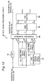
- Fig. 12 is a block diagram illustrating the fifth image processing circuit 90 depicted in Fig. 11.
- 72 is an LPF
- 85 is a horizontal sub-sampling circuit
- 38 and 42 are one pixel delay circuits
- 40 is a one horizontal period delay circuit
- 44 and 48 are subtracters
- 46 is an adder
- 56 is an RGB matrix calculation circuit
- 58 is a YUV matrix calculation circuit.
- the input colour signal with 640 pixels horizontally and 240 vertically has 340 horizontal pixels sample in the horizontal sampling circuit 85, as a result of which a Y/C output of 340 horizontal 240 vertical is obtained.
- the Y/C signal is converted to an analogue signal in the D/A converter 22 and displayed on the built-in display device 26.
- the output obtained here is an image signal of the whole valid image area of the CCD (it has not been subject to zoom processing).
- the means 96 of detecting the position of the focus outputs, for instance, a high-level signal, as a result of which the interlocking switches S1a and S1b are set in the positions denoted by the unbroken lines.
- Fig. 13 is a block diagram illustrating the sixth image processing circuit 92 depicted in Fig. 11.
- 74 is an image centre read circuit
- 76 is a vertical interpolation circuit.
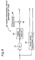
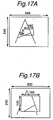
- Fig. 14 illustrates the area which is read by the image centre read circuit 20.
- a colour signal of 320 pixels horizontal' 120 vertical of the part denoted in the drawing by shading is read from the memory, and after Y/C signal processing, vertical interpolation is implemented by lining the same signal up twice or by some other method, as a result of which a Y/C output of 340 pixels horizontal 240 vertical is obtained.
- the Y/C signal is converted to an analogue signal in the D/A conversion circuit 8, and displayed on the in-built display device 26.
- the output obtained here is an image signal with the centre part of the valid image area of the CCD enlarged. Since there is no horizontal sampling in the fifth image processing circuit 90, it is possible to display a more detailed image than if the output of the fifth image processing circuit 90 were simply enlarged. Consequently, it makes it easy to adjust the focus manually while viewing the in-built display device.
- the above is the action when the shutter button has not been released. If the shutter button is released, a high-level signal is output from the flip-flop, the switches S1a and S1b are set in the positions denoted by the broken lines, and the image signal processed in the first image processing circuit is memorised in the memory 41.
- Fig. 15 illustrates a fourth embodiment of the present invention in which this has been improved.
- 78 is a circuit for generating horizontal timing
- 79 is a circuit for generating vertical timing
- 47 and 48 are AND circuits.
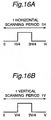
- Fig. 16 (a) and (b) are examples of output signals from the circuit for generating horizontal timing 78 and the circuit for generating vertical timing 79 respectively, while Fig. 17 (a) and (b) are colour data in the memory, and a conceptual drawing of image signals displayed on the built-in display device respectively.
- an image output is obtained in which only the centre part of the screen, amounting to one half in both the horizontal and vertical directions, is enlarged and processed. This makes it possible to adjust the focus manually while viewing the centre part of the image, and to adjust the angle while viewing the peripheral part of the image.
- the first processing circuit 10, second processing circuit 12, progressive processing circuit 8 and other circuits may be constituted using a microcomputer.
- signal processing is implemented by the processor, so that it is possible to decrease the frequency of calculation for signal processing and increase the processing speed the greater the degree of culling.
- the second embodiment was described in such a manner that both the constant values and the gamma correction circuit were changed, but it is possible to change just one of them.
- first, second, third and fourth embodiments have been described in such a manner that the first processing circuit 10, second processing circuit 12, third processing circuit 80, fourth processing circuit 82, fifth processing circuit 90, sixth processing circuit 92 and progressive processing circuit 8 are all constituted separately, but it is possible for the first processing circuit 10, second processing circuit 12, third processing circuit 80, fourth processing circuit 82, fifth processing circuit 90, sixth processing circuit 92 and progressive processing circuit 8 to be constituted as one circuit by changing clock frequencies and providing a switch arrangement whereby additional circuits can be attached and detached.
- first, second, third and fourth embodiments have been described in such a manner that the second interlocking switches S2a and S2b have been changed in accordance with the output from the detector 14 which detects whether the video cable has been inserted or not, or from the device 96 for detecting the position of the focus, but this can be implemented manually or by other means.
Landscapes
- Engineering & Computer Science (AREA)
- Multimedia (AREA)
- Signal Processing (AREA)
- Studio Devices (AREA)
- Controls And Circuits For Display Device (AREA)
- Details Of Cameras Including Film Mechanisms (AREA)
- Television Signal Processing For Recording (AREA)
Applications Claiming Priority (7)
| Application Number | Priority Date | Filing Date | Title |
|---|---|---|---|
| JP773497 | 1997-01-20 | ||
| JP773497 | 1997-01-20 | ||
| JP15971597 | 1997-06-17 | ||
| JP15971597A JP3588409B2 (ja) | 1997-01-20 | 1997-06-17 | 表示切り替え式デジタルカメラ |
| JP20749697 | 1997-08-01 | ||
| JP9207496A JPH1155560A (ja) | 1997-08-01 | 1997-08-01 | デジタルカメラ |
| EP98300260A EP0854642A3 (fr) | 1997-01-20 | 1998-01-15 | Caméra numérique avec dispositifs d'affichage interchangeables |
Related Parent Applications (1)
| Application Number | Title | Priority Date | Filing Date |
|---|---|---|---|
| EP98300260A Division EP0854642A3 (fr) | 1997-01-20 | 1998-01-15 | Caméra numérique avec dispositifs d'affichage interchangeables |
Publications (2)
| Publication Number | Publication Date |
|---|---|
| EP1526720A2 true EP1526720A2 (fr) | 2005-04-27 |
| EP1526720A3 EP1526720A3 (fr) | 2005-05-11 |
Family
ID=27277729
Family Applications (3)
| Application Number | Title | Priority Date | Filing Date |
|---|---|---|---|
| EP98300260A Ceased EP0854642A3 (fr) | 1997-01-20 | 1998-01-15 | Caméra numérique avec dispositifs d'affichage interchangeables |
| EP05000883A Withdrawn EP1526720A3 (fr) | 1997-01-20 | 1998-01-15 | Caméra numérique avec dispositifs d'affichage interchangeables |
| EP05000882A Expired - Lifetime EP1531619B1 (fr) | 1997-01-20 | 1998-01-15 | Caméra numérique avec dispositifs d'affichage interchangeables |
Family Applications Before (1)
| Application Number | Title | Priority Date | Filing Date |
|---|---|---|---|
| EP98300260A Ceased EP0854642A3 (fr) | 1997-01-20 | 1998-01-15 | Caméra numérique avec dispositifs d'affichage interchangeables |
Family Applications After (1)
| Application Number | Title | Priority Date | Filing Date |
|---|---|---|---|
| EP05000882A Expired - Lifetime EP1531619B1 (fr) | 1997-01-20 | 1998-01-15 | Caméra numérique avec dispositifs d'affichage interchangeables |
Country Status (4)
| Country | Link |
|---|---|
| US (3) | US6753917B2 (fr) |
| EP (3) | EP0854642A3 (fr) |
| CN (2) | CN1258281C (fr) |
| DE (1) | DE69839316T2 (fr) |
Families Citing this family (19)
| Publication number | Priority date | Publication date | Assignee | Title |
|---|---|---|---|---|
| JP2000050129A (ja) * | 1998-07-31 | 2000-02-18 | Minolta Co Ltd | デジタルカメラ |
| US20020067435A1 (en) * | 1998-12-21 | 2002-06-06 | Mark Rapaich | Digital yuv video equalization gamma and correction |
| JP2001054013A (ja) * | 1999-08-13 | 2001-02-23 | Fuji Photo Film Co Ltd | 撮像信号処理装置およびその処理方法 |
| JP2001211351A (ja) * | 2000-01-27 | 2001-08-03 | Fuji Photo Film Co Ltd | 画像撮像装置およびその動作制御方法 |
| JP2002314863A (ja) * | 2001-04-18 | 2002-10-25 | Konica Corp | 電子カメラ |
| JP3720766B2 (ja) * | 2002-01-25 | 2005-11-30 | キヤノン株式会社 | 焦点調節装置、撮像装置、焦点調節方法、焦点調節装置の制御プログラム、及び記憶媒体 |
| US7430577B2 (en) * | 2002-09-24 | 2008-09-30 | Interdigital Technology Corporation | Computationally efficient mathematical engine |
| US20050028102A1 (en) * | 2003-07-29 | 2005-02-03 | Schinner Charles Edward | Systems and methods for resuming a mode of display device operation |
| US7508426B2 (en) * | 2004-05-17 | 2009-03-24 | Sony Corporation | Image pickup device, and driving controlling method for solid-state imaging device |
| JP4862267B2 (ja) * | 2005-03-10 | 2012-01-25 | セイコーエプソン株式会社 | 画像表示装置 |
| JP2007028283A (ja) * | 2005-07-19 | 2007-02-01 | Matsushita Electric Ind Co Ltd | 撮像装置 |
| TW200808067A (en) * | 2006-07-31 | 2008-02-01 | Univ Nat Cheng Kung | Prediction module |
| KR101356269B1 (ko) * | 2009-09-08 | 2014-01-29 | 주식회사 팬택 | 듀얼 카메라를 지원하는 이동 단말 및 그 이동 단말의 이미지 처리 방법 |
| JP5218388B2 (ja) * | 2009-12-25 | 2013-06-26 | カシオ計算機株式会社 | 撮像装置、撮像装置の制御方法、およびプログラム |
| JP5906427B2 (ja) | 2011-06-28 | 2016-04-20 | パナソニックIpマネジメント株式会社 | 撮像装置、画像処理装置 |
| JP5903658B2 (ja) | 2011-06-28 | 2016-04-13 | パナソニックIpマネジメント株式会社 | 撮像装置 |
| EP3185568A1 (fr) | 2015-12-23 | 2017-06-28 | Samsung Electronics Co., Ltd. | Appareil d'affichage et procédé de commande pour connecter des sources externes |
| JP6752640B2 (ja) * | 2016-06-27 | 2020-09-09 | キヤノン株式会社 | 撮像装置 |
| JP2020092315A (ja) | 2018-12-04 | 2020-06-11 | キヤノン株式会社 | 表示制御装置、撮像装置、表示装置の制御方法、プログラム、および記憶媒体 |
Family Cites Families (22)
| Publication number | Priority date | Publication date | Assignee | Title |
|---|---|---|---|---|
| US4691253A (en) * | 1985-05-13 | 1987-09-01 | Polaroid Corporation | Electronic imaging camera for recording either moving or still images |
| US5070405A (en) * | 1989-09-19 | 1991-12-03 | Nikon Corporation | Electronic still camera with multi-area light metering and gray scale modification |
| US5040068A (en) * | 1989-12-28 | 1991-08-13 | Eastman Kodak Company | Electronic imaging apparatus with interchangeable pickup units |
| DE4018492C2 (de) * | 1990-06-09 | 1999-02-04 | Philips Broadcast Television S | Fernsehkamera |
| US6072526A (en) * | 1990-10-15 | 2000-06-06 | Minolta Co., Ltd. | Image sensing device that can correct colors corresponding to skin in a video signal |
| US5231159A (en) | 1990-12-27 | 1993-07-27 | The Gates Rubber Company | High temperature resistant molded elastomer |
| US5382974A (en) * | 1991-04-18 | 1995-01-17 | Fuji Photo Film Company, Limited | Movie camera having still picture photographing function and method of photographing still picture therewith |
| JPH04326874A (ja) * | 1991-04-26 | 1992-11-16 | Fuji Photo Film Co Ltd | ストロボ付ムービーカメラ |
| JPH04358479A (ja) * | 1991-06-04 | 1992-12-11 | Sony Corp | ビデオカメラ |
| US5264939A (en) * | 1992-05-29 | 1993-11-23 | Eastman Kodak Company | Apparatus and method for generating an interlaced viewing signal from the output signal of a non-interlaced camera system |
| JP2959293B2 (ja) * | 1992-07-14 | 1999-10-06 | キヤノン株式会社 | 撮像装置 |
| JP3387135B2 (ja) | 1993-01-21 | 2003-03-17 | ソニー株式会社 | ビデオカメラ |
| US5396290A (en) * | 1993-03-19 | 1995-03-07 | Eastman Kodak Company | Apparatus and method for controlling a high resolution charge coupled device image sensor to provide alternative modes of picture imaging |
| US5589879A (en) * | 1993-03-26 | 1996-12-31 | Fuji Photo Film Co., Ltd. | Performing white balance correction on integrated divided areas of which average color is substantially white |
| US6236431B1 (en) * | 1993-05-27 | 2001-05-22 | Canon Kabushiki Kaisha | Video camera apparatus with distance measurement area adjusted based on electronic magnification |
| US5650819A (en) * | 1993-09-30 | 1997-07-22 | Canon Kabushiki Kaisha | Image pickup apparatus |
| JPH07107358A (ja) * | 1993-09-30 | 1995-04-21 | Canon Inc | 撮像装置 |
| US5828406A (en) | 1994-12-30 | 1998-10-27 | Eastman Kodak Company | Electronic camera having a processor for mapping image pixel signals into color display pixels |
| GB9500178D0 (en) * | 1995-01-05 | 1995-03-01 | Thomson Consumer Electronics | Electronic recording camera |
| JPH08205035A (ja) | 1995-01-30 | 1996-08-09 | Canon Inc | 撮像装置 |
| US6011583A (en) * | 1995-09-08 | 2000-01-04 | Canon Kabushiki Kaisha | Image sensing apparatus using a non-interlace or progressive scanning type sensing device |
| JPH09163382A (ja) * | 1995-12-07 | 1997-06-20 | Toyo Ink Mfg Co Ltd | 色ずれ修正方法及び装置 |
-
1998
- 1998-01-15 EP EP98300260A patent/EP0854642A3/fr not_active Ceased
- 1998-01-15 EP EP05000883A patent/EP1526720A3/fr not_active Withdrawn
- 1998-01-15 DE DE69839316T patent/DE69839316T2/de not_active Expired - Lifetime
- 1998-01-15 EP EP05000882A patent/EP1531619B1/fr not_active Expired - Lifetime
- 1998-01-16 US US09/008,607 patent/US6753917B2/en not_active Expired - Lifetime
- 1998-01-20 CN CNB021304688A patent/CN1258281C/zh not_active Expired - Lifetime
- 1998-01-20 CN CN98100146A patent/CN1118185C/zh not_active Expired - Lifetime
-
2002
- 2002-03-28 US US10/107,484 patent/US6992716B2/en not_active Expired - Lifetime
- 2002-03-28 US US10/107,485 patent/US7019781B2/en not_active Expired - Lifetime
Also Published As
| Publication number | Publication date |
|---|---|
| EP1526720A3 (fr) | 2005-05-11 |
| US20020097325A1 (en) | 2002-07-25 |
| CN1258281C (zh) | 2006-05-31 |
| US20020101529A1 (en) | 2002-08-01 |
| EP0854642A2 (fr) | 1998-07-22 |
| DE69839316T2 (de) | 2009-04-16 |
| EP0854642A3 (fr) | 1999-10-20 |
| CN1189734A (zh) | 1998-08-05 |
| DE69839316D1 (de) | 2008-05-08 |
| US6992716B2 (en) | 2006-01-31 |
| US6753917B2 (en) | 2004-06-22 |
| EP1531619B1 (fr) | 2008-03-26 |
| CN1118185C (zh) | 2003-08-13 |
| US20030011699A1 (en) | 2003-01-16 |
| EP1531619A1 (fr) | 2005-05-18 |
| CN1494316A (zh) | 2004-05-05 |
| US7019781B2 (en) | 2006-03-28 |
Similar Documents
| Publication | Publication Date | Title |
|---|---|---|
| US6992716B2 (en) | Digital camera with interchangeable displays | |
| US5496106A (en) | System and method for generating a contrast overlay as a focus assist for an imaging device | |
| KR100666290B1 (ko) | 촬상 장치 및 촬상 방법 | |
| US6819359B1 (en) | Method and apparatus for controlling the processing of signals containing defective pixels in accordance with imaging operation mode | |
| JP3752951B2 (ja) | 撮像装置および輝度分布表示方法 | |
| US5990949A (en) | Digital still camera which displays a gamma-corrected high-quality still image upon depression of a shutter release button but without displaying an unwanted image | |
| US5581301A (en) | Image processing apparatus with adjustable low-pass optical filter characteristics | |
| EP1091572A2 (fr) | Appareil de prise d'images avec une fonction de réglage de la quantité de lumière incidente | |
| JP3588409B2 (ja) | 表示切り替え式デジタルカメラ | |
| JP2959823B2 (ja) | 画像処理装置 | |
| JPH1155560A (ja) | デジタルカメラ | |
| JP2004147229A (ja) | 画像表示制御装置、画像表示制御方法、カラー撮像装置及びビューファインダ装置 | |
| JP3421864B2 (ja) | ビデオカメラ | |
| JP3944926B2 (ja) | カメラ装置 | |
| JP3048411B2 (ja) | ビデオカメラ | |
| JP3048408B2 (ja) | ビデオカメラ | |
| KR20030040808A (ko) | 360도를 동시 촬상 가능한 촬상 장치 | |
| JP3043854B2 (ja) | カメラ装置 | |
| JP3043834B2 (ja) | ビデオカメラ | |
| JP3527859B2 (ja) | 電子内視鏡装置 | |
| JP3043855B2 (ja) | カメラ装置 | |
| JP3048410B2 (ja) | ビデオカメラ | |
| JPH10200793A (ja) | ファインダー装置及びそれを備えたカメラ | |
| JPH04316284A (ja) | ビデオカメラ装置 | |
| JPH06315155A (ja) | カラー撮像装置 |
Legal Events
| Date | Code | Title | Description |
|---|---|---|---|
| PUAI | Public reference made under article 153(3) epc to a published international application that has entered the european phase |
Free format text: ORIGINAL CODE: 0009012 |
|
| PUAL | Search report despatched |
Free format text: ORIGINAL CODE: 0009013 |
|
| 17P | Request for examination filed |
Effective date: 20050202 |
|
| AC | Divisional application: reference to earlier application |
Ref document number: 0854642 Country of ref document: EP Kind code of ref document: P |
|
| AK | Designated contracting states |
Kind code of ref document: A2 Designated state(s): DE FR GB |
|
| AK | Designated contracting states |
Kind code of ref document: A3 Designated state(s): DE FR GB |
|
| RIN1 | Information on inventor provided before grant (corrected) |
Inventor name: TANIZOE, YUKIHIRO Inventor name: FUJII, TOSHIYA Inventor name: SAKAUE, SHIGEO Inventor name: INOKUMA, KAZUYUKI |
|
| AKX | Designation fees paid |
Designated state(s): DE FR GB |
|
| RAP1 | Party data changed (applicant data changed or rights of an application transferred) |
Owner name: PANASONIC CORPORATION |
|
| 17Q | First examination report despatched |
Effective date: 20090224 |
|
| STAA | Information on the status of an ep patent application or granted ep patent |
Free format text: STATUS: THE APPLICATION IS DEEMED TO BE WITHDRAWN |
|
| 18D | Application deemed to be withdrawn |
Effective date: 20090707 |