EP1511086A1 - Lichtempfangstafel oder lichtemissionstafel und herstellungsverfahren dafür - Google Patents
Lichtempfangstafel oder lichtemissionstafel und herstellungsverfahren dafür Download PDFInfo
- Publication number
- EP1511086A1 EP1511086A1 EP02724691A EP02724691A EP1511086A1 EP 1511086 A1 EP1511086 A1 EP 1511086A1 EP 02724691 A EP02724691 A EP 02724691A EP 02724691 A EP02724691 A EP 02724691A EP 1511086 A1 EP1511086 A1 EP 1511086A1
- Authority
- EP
- European Patent Office
- Prior art keywords
- printed wiring
- light
- light emitting
- light receiving
- emitting panel
- Prior art date
- Legal status (The legal status is an assumption and is not a legal conclusion. Google has not performed a legal analysis and makes no representation as to the accuracy of the status listed.)
- Withdrawn
Links
Images


Classifications
-
- H—ELECTRICITY
- H10—SEMICONDUCTOR DEVICES; ELECTRIC SOLID-STATE DEVICES NOT OTHERWISE PROVIDED FOR
- H10H—INORGANIC LIGHT-EMITTING SEMICONDUCTOR DEVICES HAVING POTENTIAL BARRIERS
- H10H20/00—Individual inorganic light-emitting semiconductor devices having potential barriers, e.g. light-emitting diodes [LED]
- H10H20/80—Constructional details
- H10H20/81—Bodies
- H10H20/819—Bodies characterised by their shape, e.g. curved or truncated substrates
- H10H20/821—Bodies characterised by their shape, e.g. curved or truncated substrates of the light-emitting regions, e.g. non-planar junctions
-
- H—ELECTRICITY
- H10—SEMICONDUCTOR DEVICES; ELECTRIC SOLID-STATE DEVICES NOT OTHERWISE PROVIDED FOR
- H10F—INORGANIC SEMICONDUCTOR DEVICES SENSITIVE TO INFRARED RADIATION, LIGHT, ELECTROMAGNETIC RADIATION OF SHORTER WAVELENGTH OR CORPUSCULAR RADIATION
- H10F19/00—Integrated devices, or assemblies of multiple devices, comprising at least one photovoltaic cell covered by group H10F10/00, e.g. photovoltaic modules
- H10F19/80—Encapsulations or containers for integrated devices, or assemblies of multiple devices, having photovoltaic cells
-
- H—ELECTRICITY
- H10—SEMICONDUCTOR DEVICES; ELECTRIC SOLID-STATE DEVICES NOT OTHERWISE PROVIDED FOR
- H10F—INORGANIC SEMICONDUCTOR DEVICES SENSITIVE TO INFRARED RADIATION, LIGHT, ELECTROMAGNETIC RADIATION OF SHORTER WAVELENGTH OR CORPUSCULAR RADIATION
- H10F19/00—Integrated devices, or assemblies of multiple devices, comprising at least one photovoltaic cell covered by group H10F10/00, e.g. photovoltaic modules
- H10F19/90—Structures for connecting between photovoltaic cells, e.g. interconnections or insulating spacers
- H10F19/902—Structures for connecting between photovoltaic cells, e.g. interconnections or insulating spacers for series or parallel connection of photovoltaic cells
- H10F19/904—Structures for connecting between photovoltaic cells, e.g. interconnections or insulating spacers for series or parallel connection of photovoltaic cells characterised by the shapes of the structures
-
- H—ELECTRICITY
- H10—SEMICONDUCTOR DEVICES; ELECTRIC SOLID-STATE DEVICES NOT OTHERWISE PROVIDED FOR
- H10F—INORGANIC SEMICONDUCTOR DEVICES SENSITIVE TO INFRARED RADIATION, LIGHT, ELECTROMAGNETIC RADIATION OF SHORTER WAVELENGTH OR CORPUSCULAR RADIATION
- H10F77/00—Constructional details of devices covered by this subclass
- H10F77/10—Semiconductor bodies
- H10F77/14—Shape of semiconductor bodies; Shapes, relative sizes or dispositions of semiconductor regions within semiconductor bodies
- H10F77/147—Shapes of bodies
-
- H—ELECTRICITY
- H10—SEMICONDUCTOR DEVICES; ELECTRIC SOLID-STATE DEVICES NOT OTHERWISE PROVIDED FOR
- H10H—INORGANIC LIGHT-EMITTING SEMICONDUCTOR DEVICES HAVING POTENTIAL BARRIERS
- H10H20/00—Individual inorganic light-emitting semiconductor devices having potential barriers, e.g. light-emitting diodes [LED]
- H10H20/80—Constructional details
- H10H20/81—Bodies
- H10H20/819—Bodies characterised by their shape, e.g. curved or truncated substrates
-
- H—ELECTRICITY
- H10—SEMICONDUCTOR DEVICES; ELECTRIC SOLID-STATE DEVICES NOT OTHERWISE PROVIDED FOR
- H10W—GENERIC PACKAGES, INTERCONNECTIONS, CONNECTORS OR OTHER CONSTRUCTIONAL DETAILS OF DEVICES COVERED BY CLASS H10
- H10W90/00—Package configurations
-
- Y—GENERAL TAGGING OF NEW TECHNOLOGICAL DEVELOPMENTS; GENERAL TAGGING OF CROSS-SECTIONAL TECHNOLOGIES SPANNING OVER SEVERAL SECTIONS OF THE IPC; TECHNICAL SUBJECTS COVERED BY FORMER USPC CROSS-REFERENCE ART COLLECTIONS [XRACs] AND DIGESTS
- Y02—TECHNOLOGIES OR APPLICATIONS FOR MITIGATION OR ADAPTATION AGAINST CLIMATE CHANGE
- Y02E—REDUCTION OF GREENHOUSE GAS [GHG] EMISSIONS, RELATED TO ENERGY GENERATION, TRANSMISSION OR DISTRIBUTION
- Y02E10/00—Energy generation through renewable energy sources
- Y02E10/50—Photovoltaic [PV] energy
Definitions
- the present invention relates to a light receiving or light emitting panel which can be simply manufactured by mounting light receiving elements or light emitting elements in a plurality of retaining holes formed in a printed wiring sheet, and then sealing these mounted elements with a resin, and a method of manufacturing such a panel.
- an n type diffusion layer is formed on the surface of a p type semiconductor substrate, a light receiving surface electrode with a herringbone pattern is formed on the front surface side, a back surface electrode is formed on the back surface side, and the overall device is constructed as a flat-plate panel structure.
- a flat-plate solar cell panel when the angle of incidence of sunlight increases in the morning and evening, the proportion of reflected light increases, and the proportion of light that enters the panel drops.
- each spherical semiconductor element is provided with a diffusion layer, a pn junction and a pair of electrodes which are disposed on both ends of the semiconductor element with the center thereof interposed therebetween.
- Numerous solar cells of the abovementioned type are disposed in the form of a matrix having numerous rows and numerous columns, these solar cells are connected in series and parallel, and the cells are sealed in embedded form with a transparent synthetic resin, thus forming a solar cell panel.
- these solar cells are advantageous in the series connection of a plurality of solar cells; the arrangement of a plurality of solar cells in the form of a matrix, and the connection of these numerous solar cells in series and parallel, cannot be easily accomplished.
- the present applicant attempted series and parallel connections by disposing a plurality of solar cells in matrix form in a sandwich type configuration between two printed boards.
- a solar cell panel in which numerous solar cells are connected in parallel via two sheets of aluminum foil is proposed in Japanese patent laid-open publication No. 6-13633.
- a mesh is constructed from insulating warp filaments and first and second woof filaments on which different metal coating films are formed; furthermore, numerous spherical elements in which a diffusion layer is formed on the surface of a p type spherical single crystal silicon particulate are manufactured, these spherical elements are disposed in the respective eyes of the abovementioned mesh, the first woof filaments are connected to the diffusion layers, the second woof filaments are connected to the spherical single crystal silicon particulate, and these particulates are sealed by means of a synthetic resin.
- Objects of the present invention are to provide a light receiving or light emitting panel in which numerous spherical semiconductor elements, each of which has a pair of electrodes facing each other across the center, are electrically connected by means of a single printed wiring sheet, to provide a light receiving or light emitting panel that possesses flexibility, to provide a light receiving or light emitting panel that can be constructed as a thin type panel with a simple structure, and to provide a light receiving or light emitting panel in which the numerous spherical semiconductor elements can be connected by a desired connecting system selected from series connection, parallel connection and series-parallel connection.
- the light receiving or light emitting panel is a light receiving or light emitting panel in which a plurality of particulate semiconductor elements that have a light-to-electricity transducing function or electricity-to-light transducing function are incorporated in a planar fashion, characterized in that a light transmitting printed wiring sheet that is used to position, hold and electrically connect the plurality of semiconductor elements is provided, and the printed wiring sheet comprises a plurality of retaining holes disposed in a form of a matrix having a plurality of rows and a plurality of columns, through which a plurality of semiconductor elements are passed, and which hold intermediate parts in a height direction of the semiconductor elements, and printed wiring which is formed on the surface of the printed wiring sheet, and which electrically connects the plurality of semiconductor elements.
- the thickness of the light receiving or light emitting panel can be reduced compared to cases in which a pair of printed wiring sheets are disposed on both the upper and lower sides of the numerous semiconductor elements, and the amount of synthetic resin material that is used for the resin sealing of the semiconductor elements can be reduced, so that the light receiving or light emitting panel can be made thinner and lighter, and the manufacturing cost can be reduced.
- this light receiving or light emitting panel can also be constructed as a structure that can be deformed in the manner of a two dimensional or three dimensional curved surface; accordingly, this light receiving or light emitting panel is superior in terms of all-purpose applicability.
- the method according to the present invention for manufacturing a light receiving or light emitting panel is a method for manufacturing a light receiving or light emitting panel in which a plurality of particulate semiconductor elements that have a light-to-electricity transducing function or electricity-to-light transducing function are incorporated in a planar fashion, this method being characterized by comprising a first step in which a plurality of semiconductor elements and a light-transmitting printed wiring sheet material are prepared, a second step in which printed wiring that is used to connect the plurality of semiconductor elements is formed on the printed wiring sheet material, a third step in which a printed wiring sheet is manufactured by punching a plurality of retaining holes in the printed wiring sheet material in the form of a matrix that has a plurality of rows and a plurality of columns, and a fourth step in which respective semiconductor elements are inserted into the plurality of retaining holes in the printed wiring sheet, to hold intermediate portions in the direction of height of these semiconductor elements, and a pair of electrodes on each semiconductor element are electrically connected to the
- a light receiving or light emitting panel since a printed wiring sheet comprising printed wiring and a plurality of retaining holes disposed in the form of a matrix having a plurality of rows and a plurality of columns is prepared, a plurality of semiconductor elements are inserted into the plurality of retaining holes in this printed wiring sheet so that intermediate portions in the height direction of the semiconductor elements are held, and the pairs of electrodes of the semiconductor elements are electrically connected by the printed wiring, a light receiving or light emitting panel that possesses the various functions and advantages described above can be manufactured easily and relatively inexpensively.
- the fourth step it would also be possible to achieve the electrical connection of the pairs of electrodes of the semiconductor elements to the printed wiring by disposing pieces of metal with a low melting point in the vicinity of these pairs of electrodes, and irradiating these metal pieces with a heating beam.
- the present embodiment is an example of a case in which the present invention is applied to a solar cell panel as a light receiving panel. A method for manufacturing this solar cell panel, and the structure of this solar cell panel, will be described.
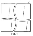
- the printed wiring sheet material 1 shown in Fig. 1 and numerous particulate semiconductor elements 2 (3600 elements in the present embodiment, hereafter referred to as "solar cells") that have a light-to-electricity transducing function, are prepared.
- the printed wiring sheet material 1 is a flat-plate material that is formed by cutting a thin transparent sheet material such as an epoxy type synthetic resin, acrylic type synthetic resin, polyester type synthetic resin, polycarbonate or the like (for example thickness 0.4 to 0.6 mm, 0.6 mm in the present embodiment) to a size of (for example) 200 mm ⁇ 200 mm.
- a thin transparent sheet material such as an epoxy type synthetic resin, acrylic type synthetic resin, polyester type synthetic resin, polycarbonate or the like (for example thickness 0.4 to 0.6 mm, 0.6 mm in the present embodiment) to a size of (for example) 200 mm ⁇ 200 mm.
- each solar cell 2 has a spherical element main body 3 consisting of p type single crystal silicon with a diameter of (e. g.) 1.5 mm, an n type diffusion layer 4 with a thickness of approximately 0.5 ⁇ m in which phosphorus (P) is diffused in the surface portion of this element main body 3, a substantially spherical pn junction 5 which is formed at the boundary between the element main body 3 and diffusion layer 4, a pair of electrodes 6, 7 (positive pole 6 and negative pole 7) which are formed facing each other on both end parts of the element main body 3 with the center of the element main body 3 interposed, and which are connected to both ends of the pn junction 5, and an SiO 2 coating film 8 (thickness of approximately, 0.4 ⁇ m) used for passivation which is formed on the surface of the diffusion layer 4 except in the areas where the pair of electrodes 6, 7 are formed.
- SiO 2 coating film 8 thinness of approximately, 0.4 ⁇ m
- Such solar cells 2 can be manufactured for example by the method proposed by the inventor of the present application in WO 98/15983.
- a small piece of p type silicon is melted, and a spherical single crystal silicon is manufactured by freely dropping this silicon from the upper end part of a dropping tube, and solidifying the silicon by radiant cooling while the silicon drops, with this silicon being maintained in a spherical shape by the action of surface tension.
- the diffusion layer 4, pair of electrodes 6, 7 and coating film 8 are formed on this spherical single crystal silicon by well known techniques such as etching, masking, a diffusion treatment and the like.
- the pair of electrodes 6, 7 are formed by respectively baking an aluminum paste or silver paste; the diameter of the electrodes 6, 7 is approximately 300 to 500 ⁇ m, and the thickness is approximately 200 to 300 ⁇ m.
- the electrodes 6, 7 may also be formed by a plating method, or may be formed by some other method.
- Each solar cell generates a photo-electromotive force with an open-circuit voltage of approximately 0.6 V when the cell receives sunlight with a light intensity of 100 mW/cm 2 .
- the solar cells 2 may also be cells in which a p type diffusion layer is formed in an n type silicon element main body, and a pair of electrodes and coating film used for passivation similar to those described above are formed.
- a flat surface 3a is formed on the side of the positive pole 6 as shown in Fig. 3 in order to allow easy discrimination of the positive pole 6 and negative pole 7 of the solar cell 2A.
- the particulate semiconductor elements need not necessarily be spherical; these semiconductor elements may also be short cylindrical solar cells 2B as shown in Fig. 4.
- Such solar cells 2B each comprise a short cylindrical element main body 10 (e.
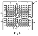
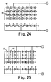
- printed wiring 20 of the type shown in the figures is formed on the printed wiring sheet material 1.
- the printed wiring 20 has a plurality of longitudinal lines 21 and a plurality of lateral lines 22 that are formed in the form of a lattice with a pitch of approximately 2.5 mm, as well as a positive pole terminal line 23 and a negative pole terminal line 24.
- the printed wiring 20 is formed by forming a solder coating film (thickness 100 ⁇ m) on the surface of a copper coating film (thickness 100 ⁇ m); the line width of the longitudinal lines 21 and lateral lines 22 is approximately 500 ⁇ m, and the line width of the positive pole terminal line 23 and negative pole terminal line 24 is approximately 5.0 mm.
- the positive pole terminal line 23 and negative pole terminal line 24 are respectively formed on the left end part and right end part of the printed wiring sheet material 1. Furthermore, as in the case of printed wiring on an ordinary printed board, this printed wiring can be formed by laminating a copper foil, and then removing unnecessary portions by etching.
- retaining holes 25 are formed by punching in the printed wiring sheet material 1, in the form of a matrix with (for example) 60 rows and 60 columns, thus producing a printed wiring sheet 26.
- a specified punching die is set in a pressing machine, and punching is performed in the printed wiring sheet material 1 on which the printed wiring 20 has been formed.
- the retaining holes 25 are holes with a regular hexagonal shape, in which the solar cells can be inserted and held.
- the retaining holes 25 of each column are disposed between one longitudinal line 21 of the printed wiring 20, an the longitudinal line 21 that is adjacent to this first longitudinal line 21, and the respective retaining holes 25 in each column are disposed so as to cut across the major portions of the lateral lines 22 between the longitudinal lines 21.
- the lateral lines 22 are connected to the portions of the outer edge parts that contact the pairs of electrodes 6, 7 of the solar cells 2 among the outer edge parts of the retaining holes 25.
- the retaining holes 25 need not necessarily have a regular hexagonal shape; these holes may have a circular shape, square shape or some other shape.
- a material that can be decomposed by the laser light of an excimer laser can be selected as the synthetic resin material that forms the printed wiring sheet material 1, and numerous retaining holes 25 can be simply formed with a high degree of precision by means of an excimer laser using a masking technique in combination.
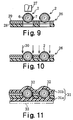
- a fourth step as is shown in Figs. 7 through 10, solar cells 2 are respectively inserted into the 3600 retaining holes 25 of the printed wiring sheet 26, so that intermediate portions in the direction of height of the solar cells 2 (intermediate portions corresponding to the electrodes 6, 7) are held, and the pairs of electrodes 6, 7 of the solar cells 2 are electrically connected to the printed wiring 20.
- the 3600 solar cells 2 are mounted with the direction of conduction arranged from right to left in Fig. 7, and the positive poles 6 and negative poles 7 of the respective solar cells 2 are connected to the corresponding lateral lines 22.
- the 3600 solar cells 22 are disposed in the form of a matrix with 60 rows and 60 columns.
- the solar cells 2 of the respective rows are connected in series by the lateral lines 22, and the solar cells 2 of the respective rows are connected in parallel by the longitudinal lines 21 on both sides.
- the positive poles 6 of the solar cells 2 of the leftmost column are connected to the positive pole terminal line 23 by a plurality of lateral lines 22, and the negative poles 7 of the solar cells 2 of the rightmost column are connected to the negative pole terminal line 24 by a plurality of lateral lines 22.
- the 3600 solar cells 2 are connected in a series-parallel connection; accordingly, even in cases where solar cells that do not operate normally are present as a result of shade or some type of trouble, the current generated by normal solar cells 2 bypasses the solar cells 2 that are not operating normally.
- the solar cells 2 are set in the retaining holes 25 so that the positive poles 6 of the solar cells 2 face the lateral lines 22 on the left side of the retaining holes 25, and so that the negative poles 7 face the lateral lines 22 on the right side of the retaining holes 25, and the solar cells 2 are inserted into the retaining holes 25 by being pressed from above by a pressing body 27, so that, as shown in Fig. 10, the positive poles 6 and negative poles 7 are caused to adhere tightly to the copper coating film 28 and solder coating film 29 of the corresponding lateral lines 22.
- the contact parts between the electrodes 6, 7 and the solder coating film 29 are irradiated with a beam 30 used for heating (i. e., a laser beam or infrared beam), so that the solder coating film 29 is fused to the electrodes 6, 7.
- a beam 30 used for heating i. e., a laser beam or infrared beam
- a coating film consisting of a soft transparent synthetic resin material e. g., an EVA resin, silicone resin or the like
- a covering material 31 that resin-seals the numerous solar cells 2 is formed.
- the covering material 31 may also be constructed from a hard transparent synthetic resin material (e. g., an acrylic type synthetic resin, epoxy type synthetic resin, polyethylene type synthetic resin, polycarbonate or the like). The covering material 31 also fills the gaps inside the respective retaining holes 25.
- the thickness of the undersurface film 31a of the covering material 31 is (for example) approximately 400 to 600 ⁇ m, and the thickness of the upper surface film 31b of the covering material 31 is (for example) approximately 200 to 400 ⁇ m.
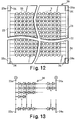
- partially cylindrical lens parts 32 that bulge outward in the direction of the upper surface are formed on the upper surfaces of the solar cells of the respective columns or respective rows.
- partially cylindrical lens parts 32 it would also be possible to form partially spherical lens parts that bulge outward in the direction of the upper surfaces of the respective solar cells 2. If the solar cells 2 of this solar cell panel 35 are indicated by diode symbols in the figures, then the equivalent circuit diagram of this solar cell panel 35 is as shown in Fig. 13.
- 3600 solar cells 2 (indicated by diode symbols in the figures) are connected in a series-parallel connection, and both end parts of the positive pole terminal line 23 constitute positive pole terminals 23a, while both end parts of the negative pole terminal line 24 constitute negative pole terminals 24a.
- recessed parts 34 in which the upper surface film 31b of the covering material 31 is not formed are respectively formed in the four corner parts of the solar cell panel 35, and the positive pole terminals 23a and negative pole terminals 24a are exposed in these recessed parts 34.
- Each solar cell 2 generates a photo-electromotive force of approximately 0.6 V when this solar cell receives sunlight with a light intensity of 100 mW/cm 2 . Since 60 solar cells 2 are connected in series in the solar cell panel 35, the maximum voltage of the electromotive force generated by sunlight in this solar cell panel 35 is approximately 36 V
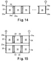
- a plurality of solar cell panels 35 can be connected in series, connected in parallel or connected in a series-parallel connection via the positive pole terminals 23a and negative pole terminals 24a.
- Fig. 14 shows an example in which a plurality of solar cell panels 35 are connected in series
- Fig. 15 shows an example in which a plurality of solar cell panels 35 are connected in a series-parallel connection.
- This solar cell panel 35 can be used in a household solar power generating system, various types of solar power generating systems used in mobile entities such as automobiles, electric trains, boats and the like, solar power generating systems used as compact power supplies in electronic equipment or electrical equipment, and other types of solar power generating systems such as chargers or the like.
- the solar cell panel 35 Since the solar cell panel 35 has a light-transmitting structure, both light from above and light from below can be received and subjected to a light-to-electricity transducing function. However, in cases where this solar cell panel 35 is used in a solar power generating system that is installed in a fixed manner, it is desirable that a reflective film 33 or reflective plate made of metal that reflects the sunlight that is incident from above toward the solar cells 2 be disposed on the undersurface side (surface on the opposite side from the light receiving surface) of the solar cell panel 35.
- the printed wiring sheet material 1 is constructed from a hard synthetic resin; however, since the covering material 31 comprises a soft synthetic resin, and since the thickness of the printed wiring sheet 26 is also small, and numerous retaining holes 25 are formed in the printed wiring sheet 26 so that this sheet is easily deformed, the solar cell panel 35 is deformable in the manner of a two dimensional or three dimensional curved surface. Accordingly, the panel can be used with the panel disposed in a state that conforms to the curved surfaces of various types of objects such as buildings or mobile entities. For example, the panel can also be used in a configuration in which the panel is bonded to the surface of an automobile body.
- the covering material 31 may also be constructed from a hard synthetic resin in such cases.
- this solar cell panel 35 a construction is used in which numerous solar cells 2 are incorporated on a single printed wiring sheet 26, intermediate parts in the direction of height of the respective solar cells 2 are held by the retaining holes 25, and the electrodes 6, 7 of the respective solar cells 2 are connected to the printed wiring 20; accordingly, the disposition, positioning and electrical connection of the numerous solar cells 2 can easily be accomplished.
- the thickness of the solar cell panel 35 can be reduced compared to a case in which a pair of printed wiring sheets are disposed above and below the numerous solar cells 2. Consequently, the amount of synthetic resin material that is required for the covering material 31 can be reduced, the solar cell panel 35 can be made thinner and lighter in weight, and the manufacturing cost can be reduced.
- the numerous solar cells 2 are connected in series and parallel by the printed wiring 20 of the printed wiring sheet 26, even solar cells 2 that show faulty operation due to shade or trouble are present, the current that is generated by the normal solar cells 2 bypasses the solar cells 2 that show faulty operation, so that the operating rate of the numerous solar cells 2 is increased.
- positive pole terminals 23a are formed on both end parts of the positive pole end part of the solar cell panel 35, and negative pole terminals 24a are formed on both end parts of the negative pole end part, and since these terminals are exposed, a plurality of solar cell panels 35 can be electrically connected, so that the structure is simplified. Furthermore, since a plurality of lens parts 32 are formed on the solar cell panel 35, sunlight easily enters even if the angle of incidence of the sunlight varies; accordingly, the sunlight utilization rate can be increased.
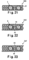
- This light emitting device 60 is constructed from an inner tube 61 that is formed from glass, a transparent or opaque synthetic resin, a metal or the like, a light emitting panel 62 that is bent into a cylindrical form and bonded to the surface of this inner tube 61, an outer tube 63 used as a surface protecting body made of glass or a transparent synthetic resin that is fit over this light emitting panel 62.
- a plurality of semiconductor elements 64 that have an electricity-to-light transducing function are mounted in this light emitting panel 62 in the form of a matrix that has a plurality of rows and a plurality of columns.
- the inner tube 61 instead of the inner tube 61, it would also be possible to use a semi-cylindrical body, partially cylindrical body, hollow spherical body, semi-hollow spherical body, partially hollow spherical body or curved-surface body with a curved surface consisting of the same material as that described above, and to use a construction in which a light emitting panel is bonded to the surface of one of these bodies, and a surface protecting body made of glass or a transparent synthetic resin is bonded to the surface of this light emitting panel.
Landscapes
- Photovoltaic Devices (AREA)
Applications Claiming Priority (1)
| Application Number | Priority Date | Filing Date | Title |
|---|---|---|---|
| PCT/JP2002/004415 WO2003094248A1 (fr) | 2002-05-02 | 2002-05-02 | Panneau recepteur de lumiere ou panneau emetteur de lumiere, et procede de fabrication de celui-ci |
Publications (2)
| Publication Number | Publication Date |
|---|---|
| EP1511086A1 true EP1511086A1 (de) | 2005-03-02 |
| EP1511086A4 EP1511086A4 (de) | 2007-02-28 |
Family
ID=29287951
Family Applications (1)
| Application Number | Title | Priority Date | Filing Date |
|---|---|---|---|
| EP02724691A Withdrawn EP1511086A4 (de) | 2002-05-02 | 2002-05-02 | Lichtempfangstafel oder lichtemissionstafel und herstellungsverfahren dafür |
Country Status (9)
| Country | Link |
|---|---|
| US (1) | US7238966B2 (de) |
| EP (1) | EP1511086A4 (de) |
| JP (1) | JP3902210B2 (de) |
| KR (1) | KR100652916B1 (de) |
| CN (1) | CN100426530C (de) |
| AU (1) | AU2002255303B2 (de) |
| CA (1) | CA2483363C (de) |
| TW (1) | TW550830B (de) |
| WO (1) | WO2003094248A1 (de) |
Cited By (5)
| Publication number | Priority date | Publication date | Assignee | Title |
|---|---|---|---|---|
| ITRM20110439A1 (it) * | 2011-08-11 | 2013-02-12 | Alfredo Chiacchieroni | Deposito brevetto d'invenzione dal titolo "modulo fotovoltaico a diodi a emissione luminosa" |
| EP2478290A4 (de) * | 2009-09-15 | 2014-01-15 | Nthdegree Tech Worldwide Inc | Lichtemittierende, photovoltaische oder andere elektronische vorrichtung sowie system und herstellungsverfahren dafür |
| EP2610919A4 (de) * | 2010-08-26 | 2014-05-14 | Kyosemi Corp | Maschengewebesubstrat mit halbleitern sowie verfahren und vorrichtung zu seiner herstellung |
| WO2015001579A1 (en) | 2013-07-04 | 2015-01-08 | IPEB Srl | Photovoltaic module using light emitting diodes |
| US9777914B2 (en) | 2007-05-31 | 2017-10-03 | Nthdegree Technologies Worldwide Inc. | Light emitting apparatus having at least one reverse-biased light emitting diode |
Families Citing this family (63)
| Publication number | Priority date | Publication date | Assignee | Title |
|---|---|---|---|---|
| WO2003017383A1 (fr) * | 2001-08-13 | 2003-02-27 | Josuke Nakata | Dispositif a semi-conducteur et procede de fabrication correspondant |
| WO2003017382A1 (en) * | 2001-08-13 | 2003-02-27 | Josuke Nakata | Light-emitting or light-receiving semiconductor module and method of its manufacture |
| EP1445804A4 (de) * | 2001-10-19 | 2008-03-05 | Josuke Nakata | Lichtemissions- oder lichtempfangshalbleitermodul und verfahren zu seiner herstellung |
| KR100652916B1 (ko) | 2002-05-02 | 2006-12-01 | 죠스케 나카다 | 수광 또는 발광용 패널 및 그 제조 방법 |
| ES2315367T3 (es) | 2002-06-21 | 2009-04-01 | Kyosemi Corporation | Dispositivo receptor de luz o emisor de luz y su metodo de produccion. |
| US7387400B2 (en) * | 2003-04-21 | 2008-06-17 | Kyosemi Corporation | Light-emitting device with spherical photoelectric converting element |
| EP1901419B1 (de) * | 2003-06-09 | 2009-03-11 | Kyosemi Corporation | Generatorsystem |
| WO2005041312A1 (ja) * | 2003-10-24 | 2005-05-06 | Kyosemi Corporation | 受光又は発光モジュールシート及びその製造方法 |
| JP4780951B2 (ja) * | 2003-11-27 | 2011-09-28 | 京セラ株式会社 | 光電変換装置 |
| MX2007007939A (es) | 2004-12-27 | 2007-11-07 | Quantum Paper Inc | Dispositivo de representacion visual emisivo direccionable e imprimible. |
| WO2007034537A1 (ja) | 2005-09-20 | 2007-03-29 | Renesas Technology Corp. | Led光源およびその製造方法 |
| EP2040313A4 (de) * | 2006-07-04 | 2010-08-25 | Kyosemi Corp | Panel-förmiges halbleitermodul |
| TWI466304B (zh) * | 2006-07-07 | 2014-12-21 | Energy Related Devices Inc | 與球形光伏特電池彈性耦合的微型集中器 |
| CN101479857B (zh) * | 2006-07-07 | 2011-03-16 | 京半导体股份有限公司 | 面板形半导体模块 |
| CN101507001B (zh) * | 2006-08-07 | 2012-09-19 | 京半导体股份有限公司 | 发电或发光用半导体模块 |
| US20090165838A1 (en) * | 2007-01-24 | 2009-07-02 | Beck Wiiliam Bill | Coated solar panel |
| JP5100180B2 (ja) * | 2007-03-30 | 2012-12-19 | パナソニック株式会社 | 発光素子および製造方法 |
| US9425357B2 (en) | 2007-05-31 | 2016-08-23 | Nthdegree Technologies Worldwide Inc. | Diode for a printable composition |
| US8384630B2 (en) | 2007-05-31 | 2013-02-26 | Nthdegree Technologies Worldwide Inc | Light emitting, photovoltaic or other electronic apparatus and system |
| US8809126B2 (en) | 2007-05-31 | 2014-08-19 | Nthdegree Technologies Worldwide Inc | Printable composition of a liquid or gel suspension of diodes |
| US8674593B2 (en) | 2007-05-31 | 2014-03-18 | Nthdegree Technologies Worldwide Inc | Diode for a printable composition |
| US9419179B2 (en) | 2007-05-31 | 2016-08-16 | Nthdegree Technologies Worldwide Inc | Diode for a printable composition |
| US8846457B2 (en) | 2007-05-31 | 2014-09-30 | Nthdegree Technologies Worldwide Inc | Printable composition of a liquid or gel suspension of diodes |
| US8415879B2 (en) | 2007-05-31 | 2013-04-09 | Nthdegree Technologies Worldwide Inc | Diode for a printable composition |
| US9534772B2 (en) | 2007-05-31 | 2017-01-03 | Nthdegree Technologies Worldwide Inc | Apparatus with light emitting diodes |
| US8877101B2 (en) | 2007-05-31 | 2014-11-04 | Nthdegree Technologies Worldwide Inc | Method of manufacturing a light emitting, power generating or other electronic apparatus |
| US8133768B2 (en) | 2007-05-31 | 2012-03-13 | Nthdegree Technologies Worldwide Inc | Method of manufacturing a light emitting, photovoltaic or other electronic apparatus and system |
| US9343593B2 (en) | 2007-05-31 | 2016-05-17 | Nthdegree Technologies Worldwide Inc | Printable composition of a liquid or gel suspension of diodes |
| US8889216B2 (en) | 2007-05-31 | 2014-11-18 | Nthdegree Technologies Worldwide Inc | Method of manufacturing addressable and static electronic displays |
| US8852467B2 (en) | 2007-05-31 | 2014-10-07 | Nthdegree Technologies Worldwide Inc | Method of manufacturing a printable composition of a liquid or gel suspension of diodes |
| US8013238B2 (en) * | 2007-07-09 | 2011-09-06 | Energy Related Devices, Inc. | Micro concentrators elastically coupled with spherical photovoltaic cells |
| TW200924232A (en) * | 2007-11-26 | 2009-06-01 | Lin Pin Ya | Light emitting diode capable of radiating light and dissipating heat in dual directions |
| US8127477B2 (en) | 2008-05-13 | 2012-03-06 | Nthdegree Technologies Worldwide Inc | Illuminating display systems |
| US7992332B2 (en) | 2008-05-13 | 2011-08-09 | Nthdegree Technologies Worldwide Inc. | Apparatuses for providing power for illumination of a display object |
| KR101439386B1 (ko) * | 2008-08-08 | 2014-09-16 | 스페라 파워 가부시키가이샤 | 채광형 태양전지 모듈 |
| DE102008038184A1 (de) * | 2008-08-19 | 2010-02-25 | Suss Microtec Test Systems Gmbh | Verfahren und Vorrichtung zur temporären elektrischen Kontaktierung einer Solarzelle |
| US20100101627A1 (en) * | 2008-10-26 | 2010-04-29 | Patel Pradyumna V | Flexible solar panel module |
| KR101267545B1 (ko) | 2009-02-27 | 2013-05-24 | 도시바 라이텍쿠 가부시키가이샤 | 발광모듈 및 조명장치 |
| US8723016B2 (en) * | 2009-07-14 | 2014-05-13 | Honeywell International Inc. | Low profile solar concentrator |
| WO2011023139A1 (en) * | 2009-08-31 | 2011-03-03 | Byd Company Limited | Solar battery assembly |
| JP5430767B2 (ja) * | 2010-08-26 | 2014-03-05 | 京セミ株式会社 | 半導体素子付き織網基材、その製造方法及びその製造装置 |
| FR2964176B1 (fr) * | 2010-09-01 | 2015-10-16 | Saint Gobain | Panneau decoratif et eclairant a diodes electroluminescentes |
| KR101316943B1 (ko) | 2010-09-30 | 2013-10-18 | 한국에너지기술연구원 | 실리콘 구립체 기반 태양전지 제조방법 및 이에 의하여 제조된 태양전지 |
| CN102194906B (zh) * | 2011-04-29 | 2012-10-10 | 浙江吉利汽车研究院有限公司 | 一种太阳能电池板的集成结构 |
| US9391226B2 (en) | 2011-11-10 | 2016-07-12 | Lei Guo | Semiconductor DC transformer |
| CN102569489B (zh) * | 2012-01-20 | 2016-01-27 | 郭磊 | 一种半导体直流变压器 |
| TWI506801B (zh) | 2011-12-09 | 2015-11-01 | 鴻海精密工業股份有限公司 | 太陽能電池組 |
| CN103165690B (zh) | 2011-12-16 | 2015-11-25 | 清华大学 | 太阳能电池 |
| CN103165719B (zh) | 2011-12-16 | 2016-04-13 | 清华大学 | 太阳能电池 |
| CN103178137B (zh) * | 2011-12-22 | 2016-04-13 | 清华大学 | 太阳能电池组 |
| CN103178123B (zh) * | 2011-12-22 | 2016-08-10 | 清华大学 | 太阳能电池基座 |
| CN103178136B (zh) * | 2011-12-22 | 2016-01-20 | 清华大学 | 太阳能电池组 |
| CN103187456B (zh) | 2011-12-29 | 2015-08-26 | 清华大学 | 太阳能电池 |
| CN103187453B (zh) | 2011-12-29 | 2016-04-13 | 清华大学 | 太阳能电池 |
| CN103187476B (zh) | 2011-12-29 | 2016-06-15 | 清华大学 | 太阳能电池的制备方法 |
| JP6024529B2 (ja) * | 2013-03-11 | 2016-11-16 | 株式会社豊田自動織機 | 太陽電池モジュール、および太陽電池モジュールの製造方法 |
| US9525097B2 (en) | 2013-03-15 | 2016-12-20 | Nthdegree Technologies Worldwide Inc. | Photovoltaic module having printed PV cells connected in series by printed conductors |
| US9957037B2 (en) | 2013-07-10 | 2018-05-01 | X Development Llc | High altitude aircraft with integrated solar cells, and associated systems and methods |
| JP2015050413A (ja) * | 2013-09-04 | 2015-03-16 | アン,ヒョン・ウー | Pcbを利用した太陽電池 |
| KR101464088B1 (ko) * | 2013-11-26 | 2015-01-21 | 희성전자 주식회사 | 태양전지의 전극 구조 및 그 형성 방법 |
| EP3255682B1 (de) | 2015-02-06 | 2020-11-04 | Dow-Mitsui Polychemicals Co., Ltd. | Verdrahtungsplatte, struktur und fotovoltaisches erzeugungsmodul |
| TWI590433B (zh) * | 2015-10-12 | 2017-07-01 | 財團法人工業技術研究院 | 發光元件以及顯示器的製作方法 |
| CN113707787B (zh) * | 2020-05-22 | 2023-07-18 | 重庆康佳光电技术研究院有限公司 | 球形倒装微型led及其制造方法、显示面板 |
Family Cites Families (58)
| Publication number | Priority date | Publication date | Assignee | Title |
|---|---|---|---|---|
| US3038952A (en) | 1959-05-20 | 1962-06-12 | Hoffman Electronics Corp | Method of making a solar cell panel |
| US3350775A (en) | 1963-10-03 | 1967-11-07 | Hoffman Electronics Corp | Process of making solar cells or the like |
| US3433676A (en) | 1964-10-21 | 1969-03-18 | Gen Motors Corp | Thermophotovoltaic energy convertor with photocell mount |
| DE1539564A1 (de) | 1966-11-09 | 1969-12-11 | Siemens Ag | Lumineszenzdiode mit hohem Wirkungsgrad |
| US3998659A (en) | 1974-01-28 | 1976-12-21 | Texas Instruments Incorporated | Solar cell with semiconductor particles and method of fabrication |
| JPS5328751B2 (de) | 1974-11-27 | 1978-08-16 | ||
| US4021323A (en) | 1975-07-28 | 1977-05-03 | Texas Instruments Incorporated | Solar energy conversion |
| US4126812A (en) | 1976-12-20 | 1978-11-21 | Texas Instruments Incorporated | Spherical light emitting diode element and character display with integral reflector |
| US4521640A (en) | 1981-09-08 | 1985-06-04 | Texas Instruments Incorporated | Large area, low temperature process, fault tolerant solar energy converter |
| FR2548563B1 (fr) | 1983-07-06 | 1985-11-22 | Stein Industrie | Ensemble forme par l'assemblage de tubes en acier inoxydable ferritique sur une plaque tubulaire en acier au carbone, et procede de fabrication dudit ensemble |
| US4582588A (en) | 1984-09-04 | 1986-04-15 | Texas Instruments Incorporated | Method of anodizing and sealing aluminum |
| US4691076A (en) | 1984-09-04 | 1987-09-01 | Texas Instruments Incorporated | Solar array with aluminum foil matrix |
| US4581103A (en) | 1984-09-04 | 1986-04-08 | Texas Instruments Incorporated | Method of etching semiconductor material |
| JPH0754855B2 (ja) | 1984-09-04 | 1995-06-07 | テキサス インスツルメンツ インコーポレイテッド | ソーラー・アレーの製造方法 |
| JPH01179374A (ja) | 1988-01-05 | 1989-07-17 | Res Dev Corp Of Japan | 接合型半導体発光素子 |
| US5028546A (en) | 1989-07-31 | 1991-07-02 | Texas Instruments Incorporated | Method for manufacture of solar cell with foil contact point |
| JPH0536997A (ja) | 1991-07-26 | 1993-02-12 | Sanyo Electric Co Ltd | 光起電力装置 |
| US5428249A (en) | 1992-07-15 | 1995-06-27 | Canon Kabushiki Kaisha | Photovoltaic device with improved collector electrode |
| US5419782A (en) | 1993-05-11 | 1995-05-30 | Texas Instruments Incorporated | Array of solar cells having an optically self-aligning, output-increasing, ambient-protecting coating |
| US5538902A (en) | 1993-06-29 | 1996-07-23 | Sanyo Electric Co., Ltd. | Method of fabricating a photovoltaic device having a three-dimensional shape |
| US5469020A (en) * | 1994-03-14 | 1995-11-21 | Massachusetts Institute Of Technology | Flexible large screen display having multiple light emitting elements sandwiched between crossed electrodes |
| US5466301A (en) * | 1994-06-29 | 1995-11-14 | Texas Instruments Incorporated | Solar cell having an output-increasing, protective cover |
| US5498576A (en) * | 1994-07-22 | 1996-03-12 | Texas Instruments Incorporated | Method and apparatus for affixing spheres to a foil matrix |
| US5431127A (en) | 1994-10-14 | 1995-07-11 | Texas Instruments Incorporated | Process for producing semiconductor spheres |
| JPH08199513A (ja) | 1995-01-27 | 1996-08-06 | Furetsudo:Kk | 発光標識装置 |
| JPH0949213A (ja) | 1995-08-08 | 1997-02-18 | S T Energ Kk | 路面設置型道路信号装置 |
| JPH09162434A (ja) * | 1995-12-05 | 1997-06-20 | Hitachi Ltd | 太陽電池およびその製造方法 |
| JP3231244B2 (ja) | 1996-07-22 | 2001-11-19 | 仗祐 中田 | 無機材料製の球状体の製造方法及びその製造装置 |
| WO1998015983A1 (fr) | 1996-10-09 | 1998-04-16 | Josuke Nakata | Dispositif a semi-conducteurs |
| US6204545B1 (en) | 1996-10-09 | 2001-03-20 | Josuke Nakata | Semiconductor device |
| US5925897A (en) | 1997-02-14 | 1999-07-20 | Oberman; David B. | Optoelectronic semiconductor diodes and devices comprising same |
| WO1999010935A1 (fr) | 1997-08-27 | 1999-03-04 | Josuke Nakata | Dispositif semi-conducteur spherique, procede de fabrication associe et materiau pour dispositif semi-conducteur spherique |
| WO1999038215A1 (en) | 1998-01-23 | 1999-07-29 | Josuke Nakata | Solar battery module for optical electrolysis device and optical electrolysis device |
| JPH11238897A (ja) | 1998-02-23 | 1999-08-31 | Canon Inc | 太陽電池モジュール製造方法および太陽電池モジュール |
| JP2000022184A (ja) * | 1998-07-03 | 2000-01-21 | Nippon Telegr & Teleph Corp <Ntt> | 球状または棒状結晶太陽電池およびその製造方法 |
| JP2000259992A (ja) | 1999-03-12 | 2000-09-22 | Sekisui Jushi Co Ltd | メンテナンス表示システム |
| JP2001102618A (ja) | 1999-09-30 | 2001-04-13 | Sony Corp | 受光装置 |
| JP4510961B2 (ja) * | 1999-10-19 | 2010-07-28 | Okiセミコンダクタ株式会社 | 光モジュール |
| JP2001210843A (ja) | 1999-11-17 | 2001-08-03 | Fuji Mach Mfg Co Ltd | 光発電パネルおよびその製造方法 |
| JP3091846B1 (ja) | 1999-11-26 | 2000-09-25 | 株式会社三井ハイテック | 太陽電池を含む球状半導体及びそれを用いた球状半導体装置 |
| KR100336779B1 (ko) | 1999-12-08 | 2002-05-16 | 박종섭 | 반도체 소자의 게이트 절연막 형성방법 |
| JP4276758B2 (ja) * | 1999-12-09 | 2009-06-10 | 仗祐 中田 | 球状半導体素子を用いた発電装置および球状半導体素子を用いた発光装置 |
| JP2001177132A (ja) | 1999-12-16 | 2001-06-29 | Mitsui High Tec Inc | 球体の切断方法、これを用いた太陽電池およびその製造方法 |
| JP3369525B2 (ja) | 2000-01-27 | 2003-01-20 | 株式会社三井ハイテック | 太陽電池及びその製造方法 |
| JP3436723B2 (ja) * | 2000-03-23 | 2003-08-18 | 株式会社三井ハイテック | 太陽電池の製造方法及び太陽電池 |
| US6355873B1 (en) * | 2000-06-21 | 2002-03-12 | Ball Semiconductor, Inc. | Spherical shaped solar cell fabrication and panel assembly |
| JP3939082B2 (ja) | 2000-08-03 | 2007-06-27 | 株式会社三井ハイテック | 太陽電池の製造方法 |
| AU773312B2 (en) | 2000-10-20 | 2004-05-20 | Sphelar Power Corporation | Light-emitting or light-receiving semiconductor device and method for fabricating the same |
| EP1255303B1 (de) | 2000-10-20 | 2016-06-29 | Sphelar Power Corporation | Lichtemittierendes oder lichtempfindliches halbleitermodul und seine herstellungsmethode |
| JP3490969B2 (ja) | 2000-11-24 | 2004-01-26 | 圭弘 浜川 | 光発電装置 |
| US6706959B2 (en) * | 2000-11-24 | 2004-03-16 | Clean Venture 21 Corporation | Photovoltaic apparatus and mass-producing apparatus for mass-producing spherical semiconductor particles |
| WO2003017382A1 (en) | 2001-08-13 | 2003-02-27 | Josuke Nakata | Light-emitting or light-receiving semiconductor module and method of its manufacture |
| EP1445804A4 (de) | 2001-10-19 | 2008-03-05 | Josuke Nakata | Lichtemissions- oder lichtempfangshalbleitermodul und verfahren zu seiner herstellung |
| CA2469002C (en) | 2001-12-25 | 2009-01-13 | Josuke Nakata | Light-receiving or light-emitting semiconductor apparatus |
| KR100652916B1 (ko) | 2002-05-02 | 2006-12-01 | 죠스케 나카다 | 수광 또는 발광용 패널 및 그 제조 방법 |
| ES2315367T3 (es) | 2002-06-21 | 2009-04-01 | Kyosemi Corporation | Dispositivo receptor de luz o emisor de luz y su metodo de produccion. |
| US7387400B2 (en) | 2003-04-21 | 2008-06-17 | Kyosemi Corporation | Light-emitting device with spherical photoelectric converting element |
| WO2005041312A1 (ja) | 2003-10-24 | 2005-05-06 | Kyosemi Corporation | 受光又は発光モジュールシート及びその製造方法 |
-
2002
- 2002-05-02 KR KR1020047017656A patent/KR100652916B1/ko not_active Expired - Fee Related
- 2002-05-02 CN CNB028288599A patent/CN100426530C/zh not_active Expired - Fee Related
- 2002-05-02 JP JP2004502368A patent/JP3902210B2/ja not_active Expired - Fee Related
- 2002-05-02 CA CA002483363A patent/CA2483363C/en not_active Expired - Fee Related
- 2002-05-02 US US10/511,958 patent/US7238966B2/en not_active Expired - Fee Related
- 2002-05-02 AU AU2002255303A patent/AU2002255303B2/en not_active Ceased
- 2002-05-02 EP EP02724691A patent/EP1511086A4/de not_active Withdrawn
- 2002-05-02 WO PCT/JP2002/004415 patent/WO2003094248A1/ja not_active Ceased
- 2002-06-18 TW TW091113279A patent/TW550830B/zh active
Cited By (5)
| Publication number | Priority date | Publication date | Assignee | Title |
|---|---|---|---|---|
| US9777914B2 (en) | 2007-05-31 | 2017-10-03 | Nthdegree Technologies Worldwide Inc. | Light emitting apparatus having at least one reverse-biased light emitting diode |
| EP2478290A4 (de) * | 2009-09-15 | 2014-01-15 | Nthdegree Tech Worldwide Inc | Lichtemittierende, photovoltaische oder andere elektronische vorrichtung sowie system und herstellungsverfahren dafür |
| EP2610919A4 (de) * | 2010-08-26 | 2014-05-14 | Kyosemi Corp | Maschengewebesubstrat mit halbleitern sowie verfahren und vorrichtung zu seiner herstellung |
| ITRM20110439A1 (it) * | 2011-08-11 | 2013-02-12 | Alfredo Chiacchieroni | Deposito brevetto d'invenzione dal titolo "modulo fotovoltaico a diodi a emissione luminosa" |
| WO2015001579A1 (en) | 2013-07-04 | 2015-01-08 | IPEB Srl | Photovoltaic module using light emitting diodes |
Also Published As
| Publication number | Publication date |
|---|---|
| JP3902210B2 (ja) | 2007-04-04 |
| KR20050007374A (ko) | 2005-01-17 |
| KR100652916B1 (ko) | 2006-12-01 |
| CN1625812A (zh) | 2005-06-08 |
| CA2483363A1 (en) | 2003-11-13 |
| AU2002255303A1 (en) | 2003-11-17 |
| CN100426530C (zh) | 2008-10-15 |
| AU2002255303B2 (en) | 2006-07-06 |
| CA2483363C (en) | 2009-07-07 |
| US7238966B2 (en) | 2007-07-03 |
| TW550830B (en) | 2003-09-01 |
| US20060043390A1 (en) | 2006-03-02 |
| WO2003094248A1 (fr) | 2003-11-13 |
| EP1511086A4 (de) | 2007-02-28 |
| JPWO2003094248A1 (ja) | 2005-09-08 |
Similar Documents
| Publication | Publication Date | Title |
|---|---|---|
| US7238966B2 (en) | Light-receiving panel or light-emitting panel, and manufacturing method thereof | |
| EP1553638B1 (de) | Lichtempfangs- oder lichtemissionseinrichtung und verfahren zu ihrer herstellung | |
| KR100619614B1 (ko) | 발광 또는 수광용 반도체 모듈 및 그 제조 방법 | |
| JP5017459B2 (ja) | 太陽電池モジュール及びその製造方法 | |
| WO2005041312A1 (ja) | 受光又は発光モジュールシート及びその製造方法 | |
| KR101135507B1 (ko) | 수광 또는 발광용 반도체 모듈 | |
| KR20080097392A (ko) | 수광 또는 발광용 반도체 모듈 | |
| JPH06275858A (ja) | 光起電力モジュールとその製造方法 | |
| HK1080991B (en) | Light receiving or light emitting device and its production method | |
| HK1101219B (en) | Light-receiving or light emitting device and method of manufacturing the same | |
| HK1101219A (en) | Light-receiving or light emitting device and method of manufacturing the same |
Legal Events
| Date | Code | Title | Description |
|---|---|---|---|
| PUAI | Public reference made under article 153(3) epc to a published international application that has entered the european phase |
Free format text: ORIGINAL CODE: 0009012 |
|
| 17P | Request for examination filed |
Effective date: 20041122 |
|
| AK | Designated contracting states |
Kind code of ref document: A1 Designated state(s): AT BE CH CY DE DK ES FI FR GB GR IE IT LI LU MC NL PT SE TR |
|
| AX | Request for extension of the european patent |
Extension state: AL LT LV MK RO SI |
|
| DAX | Request for extension of the european patent (deleted) | ||
| A4 | Supplementary search report drawn up and despatched |
Effective date: 20070126 |
|
| RTI1 | Title (correction) |
Free format text: LIGHT-RECEIVING PANEL OR LIGHT-EMITTING PANEL, AND MANUFACTURING METHOD THEREOF |
|
| 17Q | First examination report despatched |
Effective date: 20110928 |
|
| RAP1 | Party data changed (applicant data changed or rights of an application transferred) |
Owner name: KYOSEMI CORPORATION |
|
| RIN1 | Information on inventor provided before grant (corrected) |
Inventor name: NAKATA, JOSUKE |
|
| RAP1 | Party data changed (applicant data changed or rights of an application transferred) |
Owner name: SPHELAR POWER CORPORATION |
|
| STAA | Information on the status of an ep patent application or granted ep patent |
Free format text: STATUS: THE APPLICATION HAS BEEN WITHDRAWN |
|
| 18W | Application withdrawn |
Effective date: 20160413 |