EP1493848B1 - Seed crystal of silicon carbide single crystal and method for producing ingot using same - Google Patents
Seed crystal of silicon carbide single crystal and method for producing ingot using same Download PDFInfo
- Publication number
- EP1493848B1 EP1493848B1 EP03715636A EP03715636A EP1493848B1 EP 1493848 B1 EP1493848 B1 EP 1493848B1 EP 03715636 A EP03715636 A EP 03715636A EP 03715636 A EP03715636 A EP 03715636A EP 1493848 B1 EP1493848 B1 EP 1493848B1
- Authority
- EP
- European Patent Office
- Prior art keywords
- single crystal
- silicon carbide
- carbide single
- degrees
- face
- Prior art date
- Legal status (The legal status is an assumption and is not a legal conclusion. Google has not performed a legal analysis and makes no representation as to the accuracy of the status listed.)
- Expired - Lifetime
Links
Images


Classifications
-
- C—CHEMISTRY; METALLURGY
- C30—CRYSTAL GROWTH
- C30B—SINGLE-CRYSTAL GROWTH; UNIDIRECTIONAL SOLIDIFICATION OF EUTECTIC MATERIAL OR UNIDIRECTIONAL DEMIXING OF EUTECTOID MATERIAL; REFINING BY ZONE-MELTING OF MATERIAL; PRODUCTION OF A HOMOGENEOUS POLYCRYSTALLINE MATERIAL WITH DEFINED STRUCTURE; SINGLE CRYSTALS OR HOMOGENEOUS POLYCRYSTALLINE MATERIAL WITH DEFINED STRUCTURE; AFTER-TREATMENT OF SINGLE CRYSTALS OR A HOMOGENEOUS POLYCRYSTALLINE MATERIAL WITH DEFINED STRUCTURE; APPARATUS THEREFOR
- C30B25/00—Single-crystal growth by chemical reaction of reactive gases, e.g. chemical vapour-deposition growth
- C30B25/02—Epitaxial-layer growth
- C30B25/18—Epitaxial-layer growth characterised by the substrate
- C30B25/20—Epitaxial-layer growth characterised by the substrate the substrate being of the same materials as the epitaxial layer
-
- C—CHEMISTRY; METALLURGY
- C30—CRYSTAL GROWTH
- C30B—SINGLE-CRYSTAL GROWTH; UNIDIRECTIONAL SOLIDIFICATION OF EUTECTIC MATERIAL OR UNIDIRECTIONAL DEMIXING OF EUTECTOID MATERIAL; REFINING BY ZONE-MELTING OF MATERIAL; PRODUCTION OF A HOMOGENEOUS POLYCRYSTALLINE MATERIAL WITH DEFINED STRUCTURE; SINGLE CRYSTALS OR HOMOGENEOUS POLYCRYSTALLINE MATERIAL WITH DEFINED STRUCTURE; AFTER-TREATMENT OF SINGLE CRYSTALS OR A HOMOGENEOUS POLYCRYSTALLINE MATERIAL WITH DEFINED STRUCTURE; APPARATUS THEREFOR
- C30B23/00—Single-crystal growth by condensing evaporated or sublimed materials
- C30B23/002—Controlling or regulating
- C30B23/005—Controlling or regulating flux or flow of depositing species or vapour
-
- C—CHEMISTRY; METALLURGY
- C30—CRYSTAL GROWTH
- C30B—SINGLE-CRYSTAL GROWTH; UNIDIRECTIONAL SOLIDIFICATION OF EUTECTIC MATERIAL OR UNIDIRECTIONAL DEMIXING OF EUTECTOID MATERIAL; REFINING BY ZONE-MELTING OF MATERIAL; PRODUCTION OF A HOMOGENEOUS POLYCRYSTALLINE MATERIAL WITH DEFINED STRUCTURE; SINGLE CRYSTALS OR HOMOGENEOUS POLYCRYSTALLINE MATERIAL WITH DEFINED STRUCTURE; AFTER-TREATMENT OF SINGLE CRYSTALS OR A HOMOGENEOUS POLYCRYSTALLINE MATERIAL WITH DEFINED STRUCTURE; APPARATUS THEREFOR
- C30B25/00—Single-crystal growth by chemical reaction of reactive gases, e.g. chemical vapour-deposition growth
-
- C—CHEMISTRY; METALLURGY
- C30—CRYSTAL GROWTH
- C30B—SINGLE-CRYSTAL GROWTH; UNIDIRECTIONAL SOLIDIFICATION OF EUTECTIC MATERIAL OR UNIDIRECTIONAL DEMIXING OF EUTECTOID MATERIAL; REFINING BY ZONE-MELTING OF MATERIAL; PRODUCTION OF A HOMOGENEOUS POLYCRYSTALLINE MATERIAL WITH DEFINED STRUCTURE; SINGLE CRYSTALS OR HOMOGENEOUS POLYCRYSTALLINE MATERIAL WITH DEFINED STRUCTURE; AFTER-TREATMENT OF SINGLE CRYSTALS OR A HOMOGENEOUS POLYCRYSTALLINE MATERIAL WITH DEFINED STRUCTURE; APPARATUS THEREFOR
- C30B29/00—Single crystals or homogeneous polycrystalline material with defined structure characterised by the material or by their shape
- C30B29/10—Inorganic compounds or compositions
- C30B29/36—Carbides
Definitions
- the present invention relates to a seed crystal consisting of a silicon carbide single crystal suitable for producing a substrate (wafer) for an electric power device, a high-frequency device or the like, and a method for producing an ingot using the same.
- Silicon carbide has attracted a great deal of attention as material for an environmental resistance semiconductor because of its physical and chemical properties such as excellent in heat resistance and mechanical strength, durability against radiation, and the like. Further, in recent years, demand for a silicon carbide single crystal wafer as a substrate wafer for a short wavelength optical device from blue to ultra violet light, a high-frequency high blocking voltage electron device, and the like has been increased. However, a crystal-growing technology capable to supply a large size and high-quality silicon carbide single crystal in an industrial scale and stably has not been established yet. Therefore, though silicon carbide is material for a semiconductor having many merits and possibilities as described above, practical application of this material has been hindered.
- US-A-5958132 teaches a method for the growth of a SiC single crystal using a seed crystal of SiC having an exposed face deviating from the ⁇ 0001 ⁇ plane by an angle between 60° and 120° in the direction of the ⁇ 10-10 ⁇ plane.
- JP-A-10-017399 and JP-A-11-106297 both teach growing SiC on a (11-20) surface with a range of allowed inclinations for this surface. In both no inclination is preferred.
- FIG. 1 is a diagram showing face indices of a hexagonal silicon carbide single crystal.
- the nucleation process of the crystal can be controlled because this method uses a seed crystal. Further, by controlling the ambient pressure from 100 Pa to about 15 kPa using inert gas, the growth rate of the crystal can be controlled with good reproducibility.
- a silicon carbide single crystal being a seed crystal and a silicon carbide crystal powder 101 being raw material are put into, for instance, a graphite crucible 102.
- a seed crystal (silicon carbide wafer) 104 is fixed on the inner surface of a crucible lid 103.
- the inside of the crucible 102 is heated to 2000 to 2400°C under inert gas atmosphere (133Pa to 13.3kPa) such as argon gas or the like.
- inert gas atmosphere 133Pa to 13.3kPa
- concentration gradient of the raw material gas appears inside the crucible 102 by the temperature gradient so that raw material gas diffuses toward the seed crystal 104 side by the concentration gradient.
- Single crystal growth is realized by recrystallization of the raw material gas arriving at the seed crystal 104 on the seed crystal 104 to form a growing crystal 105. At this time, it is possible to control resistivity of the growing crystal 105 by adding impurity gas in inert gas atmosphere or mixing impurity elements or their compounds in the silicon carbide crystal powder 101.
- Typical substitutional type impurities in a silicon carbide single crystal are nitrogen (n-type), boron, and aluminum (p-type).
- n-type nitrogen
- boron boron
- p-type aluminum
- Crystal polymorphism (polytype) of a silicon carbide single crystal produced by the modified Lely method are usually 6H-type and 4H-type, and these two polytype silicon carbide single crystal wafers are on the market at present.
- the 4H-type silicon carbide single crystal wafer has high electron mobility, and said to be suitable for power device usage. Note that a large size silicon carbide single crystal of 15R-type which is unstable polytype has not yet obtained at present.
- Polytype of silicon carbide single crystal is almost determined by face polarity of a ⁇ 0001 ⁇ face crystal used for crystal growth.
- ⁇ 0001 ⁇ face there are two kinds of the (0001) Si face and the (000-1) C face which are different in polarity, and the outermost surfaces of respective faces are covered with a silicon atom layer and a carbon atom layer.
- a word ⁇ 0001 ⁇ is a generic term of these two faces.
- a ⁇ 0001 ⁇ face silicon carbide single crystal wafer having a diameter of 2 inches (50 mm) to 3 inches (75 mm) is cut from a silicon carbide single crystal prepared by the above-described modified Lely method and supplied to epitaxial thin film growth and device production.
- a silicon carbide thin film When an electric power device, a high-frequency device, or the like is produced using a silicon carbide single crystal wafer, it is usually required for a silicon carbide thin film to undergo epitaxial growth on the wafer. Regarding this method, it is typical to deposit the silicon carbide thin film on a silicon carbide wafer using the so-called thermal CVD method (thermal chemical vapor deposition method). As a face direction of a silicon carbide wafer, the (0001) Si face or the (000-1) C face are usually selected.
- pinhole defects of several ⁇ m in diameter, passing through in the growth direction are contained.
- the pinhole defect is a threading dislocation called a micropipe and is succeeded as it is even during the epitaxial growth.
- the silicon carbide single crystal grown on a face perpendicular to the ⁇ 0001 ⁇ face does not contain micropipe defects, and a face perpendicular to the ⁇ 0001 ⁇ face is said to be a useful face for producing devices.
- the (11-20) wafer obtained by cutting and polishing a silicon carbide single crystal ingot grown in the [11-20] direction is suitable for preparing a high-performance silicon carbide device. Consequently, there has been a growing attention to an epitaxial thin film which has grown on a wafer having the (11-20) face.
- An object of the present invention is to provide a seed crystal which is capable to produce materials having less defects and a diameter suitable for practical application, and made of a silicon carbide single crystal, and a method for producing a silicon carbide single crystal ingot, a silicon carbide single crystal ingot, a silicon carbide single crystal wafer, a silicon carbide single crystal epitaxial substrate, a substrate for growing a silicon carbide single crystal epitaxial thin film (single crystal substrate), and a method of producing a silicon carbide single crystal epitaxial substrate.
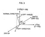
- a seed crystal consisting of a silicon carbide single crystal relating to a first invention of the present application includes a single crystal growing face inclined at an angle ranging from 3 degrees or more to 60 degrees or less with respect to the (11-20) face to a direction inclined at an angle ranging from -45 degrees or more to 45 degrees or less from a ⁇ 0001> direction to the [1-100] direction.
- a single crystal substrate consisting of a silicon carbide single crystal relating to a second invention of the present application includes an epitaxial growing face inclined at an angle ranging from 3 degrees or more to 60 degrees or less with respect to the (11-20) face to a direction inclined at an angle ranging from -45 degrees or more to 45 degrees or less from a ⁇ 0001> direction to the [1-100] direction.
- a method of producing a silicon carbide single crystal ingot relating to a third invention of the present application includes the steps of: obtaining a seed crystal consisting of a silicon carbide single crystal, and having a single crystal growing face inclined at an angle ranging from 3 degrees or more to 60 degrees or less with respect to the (11-20) face to a direction inclined at an angle ranging from -45 degrees or more to 45 degrees or less from a ⁇ 0001> direction to the [1-100] direction; and allowing to grow a silicon carbide single crystal by a sublimation recrystallization method on the single crystal growing face of said seed crystal.
- a silicon carbide single crystal ingot relating to a fourth invention of the present application is produced by the method described above, and the diameter of the ingot measures 20 mm or more.
- a silicon carbide single crystal wafer relating to a fifth invention of the present application is produced by processing and polishing the silicon carbide single crystal ingot described above, and the diameter of said wafer measures 20 mm or more.
- a silicon carbide single crystal epitaxial substrate relating to a sixth invention of the present application includes: the silicon carbide single crystal wafer described above; and a silicon carbide single crystal epitaxial film having grown on the silicon carbide single crystal wafer.
- a method of producing a silicon carbide single crystal epitaxial substrate relating to a seventh invention of the present application includes the steps of: obtaining a substrate consisting of a silicon carbide single crystal, and having a single crystal growing face inclined at an angle ranging from 3 degrees or more to 60 degrees or less with respect to the (11-20) face to a direction inclined at an angle ranging from -45 degrees or more to 45 degrees or less from a ⁇ 0001> direction to the [1-100] direction; and allowing to grow a silicon carbide single crystal epitaxial film on the single crystal growing face of the above-described substrate.
- the silicon carbide single crystal epitaxial substrate relating to an eighth invention of the present application is produced by the above-described method and the diameter of the substrate measures 20 mm or more.
- Stacking faults which have been considered as a problem are induced by capturing silicon carbide molecules not in normal arrangement but in false arrangement when the silicon carbide molecules adsorbed on the crystal are captured into the crystal.
- the silicon carbide molecules captured in false arrangement bring a local strain in the crystal, which causes generation of stacking faults.
- the mechanism to generate such a stacking fault when the silicon carbide single crystal is allowed to grow in a direction perpendicular to the ⁇ 0001 ⁇ face is described in a document " Phys. Stat. Sol. (b) from page 163 to page 175 in Vol. 202 (1997) by J. Takahashi and N. Ohtani ".
- the stacking fault in question in the present invention is a defect induced by crystal growth which is generated only during crystal growing, and is different from a crystal defect generated by applying a mechanical or an electrical stress to a crystal grown after the crystal growth.
- the present invention is achieved after the above-described mechanism has been analyzed, and as for Miller indices of silicon carbide single crystal, a face inclined by 3 degrees or more and 60 degrees or less with respect to the (11-20) face in a direction inclined by -45 degrees or more and 45 degrees or less from a ⁇ 0001> direction to the [1-100] direction is taken as a single crystal growing face (single crystal raising face).
- the angle inclined with respect to a (11-20) face of the single crystal growing face is called “off-angle” and a direction introducing the off-angle is called “off-direction” in the following explanation.
- the off-direction is in the plane including the directions ⁇ 0001> and [1-100]
- the normal line of the single crystal growing face is in the plane including the off-direction and the [11-20] direction.
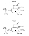
- FIG. 4A and FIG. 4B The principle of the present invention will be explained next using FIG. 4A and FIG. 4B .
- the silicon carbide molecule can take a plurality of arrangements on a crystal growing face as a bond arrangement. Namely, as shown in FIG. 4A , the silicon carbide molecule can take arrangement 21 (a bond arrangement which has completely the same bonding arrangement as that in the inside of the crystal, and is most stable in terms of energy) or arrangement 22 which is opposite in direction.
- arrangement 21 a bond arrangement which has completely the same bonding arrangement as that in the inside of the crystal, and is most stable in terms of energy
- arrangement 22 which is opposite in direction.
- the off-direction is in a direction inclined by -45 degrees or more and 45 degrees or less from a ⁇ 0001> direction to the [1-100] direction, that is, it is required to be in the range of being shifted by ⁇ 45 degrees from a ⁇ 0001> direction in the plane including the directions ⁇ 0001> and [1-100].
- the angle ⁇ in FIG. 3 is -45 degrees or more and 45 degrees or less, or 135 degrees or more and 225 degrees or less.
- the off-direction comes to be nearer to the [1-100] direction than the ⁇ 0001> direction.
- the structure of the steps and the like differ from each other.
- the off-direction comes near to the [1-100] direction, arbitrariness remains in an adsorption arrangement of silicon carbide molecules in the step so that a stacking fault can be generated. Therefore, the off-direction is required to be a direction inclined by -45 degrees or more and 45 degrees or less from a ⁇ 0001> direction to the [1-100] direction.
- a succeeding portion 23 having grown in a direction to succeed the polytype (4H-type) of the seed crystal 21 out of growing crystals 22 completely succeeds the polytype (4H-type) of the seed crystal, to exhibit a polytype of 4H-type.
- a growing direction of the succeeding portion 23 is a direction perpendicular to the ⁇ 0001> direction, for instance, the [11-20] direction.
- polytype of a non-succeeding portion 24 in which no polytype to be succeeded exists, and a polytype is not determined through succeeding from a seed crystal is determined based on a ⁇ 0001 ⁇ face which appears in a growing direction, in this case, based on the (0001) Si face. As described above, on the (0001) Si face, no polytype crystal of 4H-type grows. Accordingly, the polytype of the non-succeeding portion 24 comes to 6H-type or 6H-type with which polytype in 15R-type co-exists.
- the off-angle is 3 degrees or more and 60 degrees or less with reference to the [11-20] direction, that is, the angle ⁇ in FIG. 3 is required to be 3 degrees or more and 60 degrees or less.
- the off-angle is less than 3 degrees, since gaps between the steps on the surface of the seed crystal become too large and the density of the steps is lowered, the silicon carbide molecules are captured into the crystal even on a terrace existing between steps. At this time, since the terrace corresponds to a crystal growing face shown in FIG. 4A , the silicon carbide molecules can take a plurality of arrangements. Accordingly a stacking fault may be generated.
- an off-angle exceeds 60 degrees, growth similar to conventional growth of the silicon carbide single crystal in the ⁇ 0001> direction is performed. As a result, unfavorable micropipe defect is generated. Therefore, it is required for an off-angle to be 3 degrees or more and 60 degrees or less with reference to the [11-20] direction.
- the off-angle it is preferable for the off-angle to be an angle ranging from 3 degrees or more to 30 degrees or less, and more preferable from 6 degrees or more to 30 degrees or less.
- a method for producing a seed crystal consisting of silicon carbide single crystal according to an embodiment of the present invention will be explained next.
- a wafer is cut from a 4H-type silicon carbide single crystal which has grown in the [000-1] C direction.
- a silicon carbide single crystal ingot to be used may contain micropipe defects but should not contain stacking faults.
- a face inclined at an angle in the range from 3 degrees or more to 60 degrees or less with respect to the (11-20) face to an arbitrary direction inclined at an angle in the range from -45 degrees or more to 45 degrees or less from a ⁇ 0001> direction of the silicon carbide single crystal to the [1-100] direction is taken as the cut face.
- a seed crystal according to an embodiment of the present invention can be produced.
- the seed crystal can be used for raising silicon carbide single crystal.
- the deviation of the off-angle from the aforementioned arbitrary direction when cutting the wafer is preferably within ⁇ 1 degree.
- a 4H-type seed crystal is produced, it is recommendable to take a face inclined at an angle ranging from 3 degrees or more to 60 degrees or less with respect to the (11-20) face to an arbitrary direction inclined at an angle ranging from -45 degrees or more to 45 degrees or less from the [000-1] C direction to the [-1100] direction of the silicon carbide single crystal as the cut face.
- a silicon carbide single crystal for instance, a 4H-type silicon carbide single crystal on a seed crystal by a sublimation recrystallization method using the seed crystal consisting of silicon carbide single crystal such as a 4H-type seed crystal produced thus.
- a silicon carbide single crystal such as a 4H-type silicon carbide single crystal of good quality which has few crystal defects such as micropipe defects, stacking faults and so on with good reproducibility.
- a silicon carbide single crystal ingot such as a 4H-type silicon carbide single crystal ingot having a diameter of 20 mm or more according to this production method.
- Such a silicon carbide single crystal ingot has a merit of having no micropipe defect exerting a bad effect on a device and extremely few stacking faults while having a large diameter of, for instance, 20 mm or more.
- FIG. 6 is a diagram showing an example of the producing apparatus of a silicon carbide single crystal ingot.
- an apparatus to make silicon carbide single crystal grow by the modified Lely method using a seed crystal is explained.
- the crystal growth is performed by sublimation-recrystallizing silicon carbide powder 2 which is a raw material on silicon carbide single crystal 1 used as a seed crystal.
- the silicon carbide single crystal 1 being a seed crystal is fixed on the inside face of a lid 4 of a crucible 3 made of graphite.
- the raw material silicon carbide powder 2 is filled in the inside of the graphite crucible 3.
- the graphite crucible 3 is provided in the inside of a quartz-double tube 5 by a supporting bar 6 made of graphite.
- a felt 7 made of graphite for heat shielding is provided around the graphite crucible 3.
- the quartz-double tube 5 can be evacuated to a low pressure of 10 -3 Pa or less by a vacuum pump 11 and the inside atmosphere can be controlled in pressure by argon gas.
- the pressure control by argon gas is performed through an argon gas plumbing 9 and a mass flow controller 10 for argon gas.
- a work coil 8 is provided on the outer periphery of the quartz-double tube 5 which heats the graphite crucible 3 by flowing high-frequency electric current so as to heat the raw material and the seed crystal at a desired temperature.
- the measurement of the crucible temperature is performed by providing a light path of 2 to 4 mm in diameter at the center of the felt covering the upper portion and the lower portion of the crucible so as to let the light from the upper and lower portion of the crucible come out and by measuring with a two-color pyrometer.
- the temperature on the lower portion of the crucible 3 is taken as a raw material temperature and the temperature on the upper portion of the crucible 3 is taken as a seed temperature.
- the 4H-type silicon carbide seed crystal 1 relating to the present invention is fixed on the inside surface of the lid 4 of the graphite crucible 3 first.
- the raw material 2 is filled in the inside of the graphite crucible 3.
- the graphite crucible 3 filled with the raw material is closed with the lid 4, on which the seed crystal is fixed, and the graphite crucible 3 is placed on the graphite supporting bar 6 after covering the graphite crucible 3 with the graphite felt 7, and set in the inside of the quartz-double tube 5.
- an electric current is fed through the work coil 8 after the inside of the quart tube is evacuated and the temperature of the raw material is raised to the predetermined temperature, for instance, up to about 1600°C.
- argon gas is passed through as an atmospheric gas, and the temperature of the raw material is raised to a target temperature, for instance, up to about 2400°C, while the pressure inside the quartz tube is kept at a predetermined pressure, for instance, at about 80kPa.
- the pressure is slowly decreased to a predetermined growing pressure of, for instance, about 1.3kPa, and thereafter, by continuing growing of a single crystal for a predetermined period of time till the diameter becomes 20 mm or more, a 4H-type silicon carbide single crystal ingot can be obtained.
- a silicon carbide single crystal ingot such as a 4H-type silicon carbide single crystal ingot or the like
- a silicon carbide single crystal substrate wafer having, for instance, a diameter of 20 mm or more can be obtained.
- the silicon carbide single crystal substrate (wafer) produced thus is provided with a characteristic of having an epitaxial growing face inclined at an angle in the range from 3 degrees or more to 60 degrees or less with respect to the (11-20) face to an inclined direction at an angle ranging from -45 degrees or more to 45 degrees or less from a ⁇ 0001> direction (the [0001] Si direction or the [000-1] C direction) to the [1-100] direction, when the cut face is perpendicular to the growing direction.
- the inclined angle of the epitaxial growing face with respect to the (11-20) face becomes also from 3 degrees or more to 30 degrees or less, and when an off-angle of the used single crystal is from 6 degrees or more to 30 degrees or less, the inclined angle of the epitaxial growing face with respect to the (11-20) face becomes also from 6 degrees or more to 30 degrees or less.
- a substrate is cut from a 4H-type silicon carbide single crystal ingot which has grown in the [000-1] C direction.
- a silicon carbide single crystal ingot to be used may contain micropipe defects but no stacking fault.
- the cut face a face inclined by 3 degrees or more and 60 degrees or less with respect to the (11-20) face to an arbitrary direction inclined at an angle ranging from -45 degrees or more to 45 degrees or less from a ⁇ 0001> direction of the silicon carbide single crystal to the [1-100] direction is taken as the cut face.
- a silicon carbide single crystal substrate (wafer) can be produced.
- a deviation of the off-angle from the aforementioned arbitrary direction when cutting a wafer is preferably within ⁇ 1 degree.
- Such a silicon carbide single crystal epitaxial substrate has a merit of no micropipe defect, which exerts a bad effect on a device, and extremely few stacking faults while having a large diameter of, for instance, 20 mm or more.
- a silicon carbide single crystal substrate (wafer) according to an embodiment of the present invention is put on a susceptor made of graphite, and after putting it inside the crystal growing furnace of the thermal CVD apparatus, the inside of the crystal growing furnace is evacuated. Then, the evacuation is stopped, and after the pressure in the crystal growing furnace is returned to atmospheric pressure by introducing hydrogen gas, the susceptor is heated by induction heating while hydrogen gas is kept flowing. When the temperature of the susceptor reaches a predetermined temperature, for instance, about 1580°C, hydrogen chloride gas is allowed to flow in together with the hydrogen gas.
- the flow rates of the hydrogen gas and hydrogen chloride gas are preferably, for instance, 1.0 to 10.0 ⁇ 10 -5 m 3 /sec, 0.3 to 3.0 ⁇ 10 -7 m 3 /sec, respectively.
- the hydrogen chloride gas is stopped, the temperature is decreased to a predetermined temperature, for instance, about 800°C while the hydrogen gas is kept flowing so that the hydrogen chloride gas inside the crystal growing furnace is purged. Then, the temperature is increased to a predetermined temperature, for instance, about 1500°C to start epitaxial growth.
- the condition for growing the silicon carbide epitaxial thin film it is preferable not to be limited to a certain condition and a suitable condition is preferably selected case by case.
- the growth temperature is set to be 1500°C
- the flow rates of silane (SiH 4 ), propane (C 3 H 8 ) and hydrogen (H 2 ) are set to be 0.1 to 10.0 ⁇ 10 -9 m 3 /sec, 0.6 to 6.0 ⁇ 10 -9 m 3 /sec, 1.0 to 10.0 ⁇ 10 -5 m 3 /sec.
- the growth pressure is preferably selected suitably according to other conditions for growing, and usually atmospheric pressure is used.
- the time for growth is not limited especially and sufficient so far as a desired film thickness after growth is obtained.
- the film thickness of 1 to 20 ⁇ m can be obtained with 1 to 20 hours of the time of growth.
- the silicon carbide single crystal epitaxial substrate produced thus is extremely smooth over the entire wafer surface and has a favorable surface morphology with few surface defects caused by a micropipe defect and a stacking fault.
- a silicon carbide seed crystal 1 was obtained by mirror-like polishing the cut wafer.
- the diameter measured at this time was 20 mm at the smallest.
- the seed crystal 1 was fixed on the inside surface of a lid 4 of a graphite crucible 3.
- a raw material 2 was placed in the graphite crucible 3.
- the graphite crucible 3 filled with the raw material was covered with the lid 4, on which the seed crystal was fixed, and after covered with a graphite felt 7, it was put on the graphite supporting bar 6 to be placed inside the quartz-double tube 5.
- wafers of the (0001) face and the (1-100) face were cut and polished.
- the single crystal ingot was cut in parallel or substantially parallel to the direction of growth.
- the surfaces of the wafers were etched with molten KOH at about 530°C.
- the number of large hexagonal etch pits, which correspond to micropipe defects, in the wafer of the (0001) face, and the number of linear etch pits, which correspond to stacking faults, in the wafer of the (1-100) face were examined by microscopic observation. As a result, it was found that there was no micropipe defect at all and the stacking fault density was 4 /cm on average.
- a wafer of the (11-20) face was cut from a 6H-type silicon carbide single crystal ingot produced similarly.
- the single crystal ingot was cut substantially perpendicular to the direction of growth.
- the diameter was 22 mm.
- the wafer was polished to 300 ⁇ m in thickness to prepare a silicon carbide single crystal mirror finish wafer, the surface of which was the (11-20) face.
- the silicon carbide single crystal mirror finish wafer was used as a substrate, epitaxial growth of silicon carbide on the substrate was performed.
- the growth temperature was set to 1500°C, and the flow rates of silane (SiH 4 ), propane (C 3 H 8 ) and hydrogen (H 2 ) were set to be 5.0 ⁇ 10 -9 m 3 /sec, 3.3 ⁇ 10 -9 m 3 /sec, 5.0 ⁇ 10 -5 m 3 /sec, respectively.
- the pressure of growth atmospheric pressure was used. After 4 hours, the film thickness of the grown epitaxial thin film was about 5 ⁇ m.
- the surface morphology of the silicon carbide epitaxial thin film obtained thus was observed with Nomarski optical microscope. As a result, it was found that the wafer was very flat over its entire surface, and was good because it had very few surface defects caused by micropipe defects and stacking faults.
- this epitaxial wafer (epitaxial substrate) was cleaved at the (1-100) face, and the cleaved face was etched with molten KOH to examine the stacking fault density in the epitaxial thin film.
- the stacking fault density was 4 /cm on average, similarly to the substrate at the time of forming the epitaxial thin film.
- a silicon carbide seed crystal was obtained by mirror-like polishing the cut wafer.
- the diameter measured at this time was 20 mm at the smallest.
- the crystal was allowed to grow similarly to the first embodiment.
- the diameter of the obtained crystal was 22 mm and the height was about 16 mm.
- the wafer of the (11-20) face was cut from a single polytype silicon carbide single crystal ingot of 4H-type which was produced in a manner similar to that described above.
- the single crystal ingot was cut substantially perpendicular to the direction of growth.
- the diameter was 22 mm.
- the wafer was polished to 300 ⁇ m in thickness to prepare a silicon carbide single crystal mirror finish wafer of which surface is the (11-20) face.
- silicon carbide single crystal mirror finish wafer was used as a substrate
- silicon carbide epitaxial growth on the substrate was performed under the conditions similarly to the first embodiment.
- the grown epitaxial thin film was about 5 ⁇ m in thickness.
- the surface morphology of the silicon carbide epitaxial thin film obtained thus was observed with Nomarski optical microscope. As a result, it was found that the wafer was very flat over the entire surface thereof, and was favorable because it had very few surface defects caused by micropipe defects and stacking faults.
- this epitaxial wafer (epitaxial substrate) was cleaved at the (1-100) face, and the cleaved face was etched with molten KOH to examine the stacking fault density in the epitaxial thin film.
- the stacking fault density was 4 /cm on average, similarly to the substrate at the time of forming the epitaxial thin film.
- a silicon carbide seed crystal was obtained by mirror-like polishing the cut wafer.
- the diameter measured at this time was 20 mm at the smallest.
- the crystal was allowed to grow similarly to the first embodiment.
- the growth rate was set to 0.75 mm/sec.
- the diameter of the obtained crystal was 22 mm and the height was about 15 mm.
- the wafer of the (11-20) face was cut from a 4H-type silicon carbide single crystal ingot which was produced similarly.
- the diameter was set to 22 mm.
- the wafer was polished to 300 ⁇ m in thickness to prepare a silicon carbide single crystal mirror finish wafer having a surface of the (11-20) face.
- the silicon carbide single crystal mirror finish wafer was used as a substrate
- epitaxial growth of silicon carbide on the substrate was performed under the conditions similarly to the first embodiment.
- the thickness of the grown epitaxial thin film was about 5 ⁇ m.
- the polytype was analyzed by Raman scattering. The result showed that out of the silicon carbide single crystal mirror finish wafer, a 4H-type epitaxial thin film was formed on the 4H-type portion, and a 6H-type epitaxial thin film was formed on the 6H-type portion.
- this epitaxial wafer (epitaxial substrate) was cleaved at the (1-100) face, and the cleaved face was etched with molten KOH to examine the stacking fault density in the epitaxial thin film.
- the result showed an extremely low stacking fault density of 10 /cm or less on average except in the vicinity of the boundary between the 4H-type polytype and the 6H-type polytype.
- the stacking fault density was very high of 200 /cm.
- a silicon carbide seed crystal was obtained by mirror-like polishing the cut wafer.
- the diameter measured at this time was 20 mm at the smallest.
- the crystal was allowed to grow similarly to the first embodiment.
- the diameter of the obtained crystal was 22 mm and the height was about 16 mm.
- the wafer of the (11-20) face was cut from a 4H-type silicon carbide single crystal ingot which was produced in the same manner.
- the diameter was set to 22 mm.
- the wafer was polished to 300 ⁇ m in thickness to prepare a silicon carbide single crystal mirror finish wafer having a surface of the (11-20) face.
- the silicon carbide single crystal mirror finish wafer was used as a substrate, and epitaxial growth of silicon carbide on the substrate was performed under the conditions similarly to the first embodiment. Similarly to the first embodiment, the thickness of the grown epitaxial thin film was about 5 ⁇ m. Then, after the epitaxial thin film was allowed to grow, the surface morphology of the silicon carbide epitaxial thin film obtained thus was observed with Nomarski optical microscope. As a result, surface defects considered to be caused by stacking faults existed on the surface of the wafer.
- this epitaxial wafer (epitaxial substrate) was cleaved at the (1-100) face, and the cleaved face was etched with molten KOH to examine the stacking fault density in the epitaxial thin film.
- the result showed extremely high stacking fault density of 170 /cm on average, similarly to the substrate at the time of forming an epitaxial thin film.
- a wafer was cut from a 4H-type silicon carbide single crystal which had grown in the [000-1] C direction.
- a silicon carbide single crystal in which micropipe defects were contained but no stacking faults existed was used.
- the deviation of the off-direction from the [0001] Si direction was within ⁇ 1°.
- an epitaxial growing substrate was obtained by mirror-like polishing the cut wafer.
- the diameter measured at this time was 20 mm at the smallest.
- the epitaxial growing substrate was put on a graphite susceptor, and after putting it inside a crystal growing furnace of the thermal CVD apparatus, the inside of the crystal growing furnace was evacuated. Then, the evacuation was stopped, and after the pressure in the crystal growing furnace was returned to atmospheric pressure by introducing hydrogen gas, the susceptor was heated by induction heating while the hydrogen gas was kept flowing. When the temperature of the susceptor reached 1580°C, hydrogen chloride gas was allowed to flow in together with the hydrogen gas. The flow rates of the hydrogen gas and hydrogen chloride gas were 5.0 ⁇ 10 -5 m 3 /sec and 1.7 ⁇ 10 -7 m 3 /sec, respectively.
- the hydrogen chloride gas was stopped, the temperature was decreased to 800°C while hydrogen gas was kept flowing so that the hydrogen chloride gas inside the crystal growing furnace was purged. Then, the temperature was raised to 1500°C to start epitaxial growth.
- the growth temperature was set to be 1500°C, and the flow rates of silane (SiH 4 ), propane (C 3 H 8 ) and hydrogen (H 2 ) were set to be 5.0 ⁇ 10 -9 /sec, 3.3 ⁇ 10 -9 m 3 /sec, 5.0 ⁇ 10 -5 m 3 /sec.
- the growth pressure atmospheric pressure was used.
- the film thickness of the grown epitaxial thin film was about 5 ⁇ m.
- the surface morphology of the silicon carbide epitaxial thin film obtained thus was observed with Nomarski optical microscope. As a result, it was found that the wafer was very flat over the entire surface thereof, and was favorable because it had very few surface defects caused by micropipe defects and stacking faults.
- this epitaxial wafer (epitaxial substrate) was cleaved at the (1-100) face, and the cleaved face was etched with molten KOH to examine the stacking fault density in the epitaxial thin film. As a result, no etch pit corresponding to stacking faults was observed at all.
- a wafer was cut from the 4H-type silicon carbide single crystal which had grown in the [000-1] C direction.
- a silicon carbide single crystal in which micropipe defects were contained but no stacking faults existed was used.
- the deviation of this surface from the [11-20] direction was set to be within ⁇ 0.5°.
- an epitaxial growing substrate was obtained by mirror-like polishing the cut wafer.
- the diameter measured at this time was 20 mm at the smallest.
- the thickness of the epitaxial thin film obtained thus was about 5 ⁇ m.
- this epitaxial wafer (epitaxial substrate) was cleaved at the (1-100) face, and the cleaved face was etched with molten KOH to examine the stacking fault density in the epitaxial thin film. As a result, it was found that the stacking fault density was 10 /cm in the epitaxial thin film.
- the present invention it is possible to obtain material consisting of a silicon carbide single crystal of favorable quality, which has few crystal defects such as micropipe defects and stacking faults, and the diameter is suitable for practical application.
- a wafer made of such a silicon carbide single crystal it is possible to produce a blue light-emitting device excellent in optical characteristics, an electronic device excellent in electric characteristics and the like.
- an electric power device with an exceptionally low power loss compared with a conventional device can be produced.
Applications Claiming Priority (7)
| Application Number | Priority Date | Filing Date | Title |
|---|---|---|---|
| JP2002102683A JP4160770B2 (ja) | 2002-04-04 | 2002-04-04 | 4h型炭化珪素単結晶エピタキシャル基板 |
| JP2002102682A JP4160769B2 (ja) | 2002-04-04 | 2002-04-04 | 炭化珪素単結晶インゴット及びウエハ |
| JP2002102682 | 2002-04-04 | ||
| JP2002102683 | 2002-04-04 | ||
| JP2002152966 | 2002-05-27 | ||
| JP2002152966A JP4157326B2 (ja) | 2002-05-27 | 2002-05-27 | 4h型炭化珪素単結晶インゴット及びウエハ |
| PCT/JP2003/004058 WO2003085175A1 (fr) | 2002-04-04 | 2003-03-31 | Cristal germe de monocristal de carbure de silicium et procede de production de lingot au moyen de celui-ci |
Publications (3)
| Publication Number | Publication Date |
|---|---|
| EP1493848A1 EP1493848A1 (en) | 2005-01-05 |
| EP1493848A4 EP1493848A4 (en) | 2007-08-22 |
| EP1493848B1 true EP1493848B1 (en) | 2010-12-08 |
Family
ID=28794776
Family Applications (1)
| Application Number | Title | Priority Date | Filing Date |
|---|---|---|---|
| EP03715636A Expired - Lifetime EP1493848B1 (en) | 2002-04-04 | 2003-03-31 | Seed crystal of silicon carbide single crystal and method for producing ingot using same |
Country Status (6)
| Country | Link |
|---|---|
| US (4) | US20050160965A1 (ko) |
| EP (1) | EP1493848B1 (ko) |
| KR (1) | KR100773624B1 (ko) |
| AT (1) | ATE491055T1 (ko) |
| DE (1) | DE60335252D1 (ko) |
| WO (1) | WO2003085175A1 (ko) |
Families Citing this family (23)
| Publication number | Priority date | Publication date | Assignee | Title |
|---|---|---|---|---|
| DE10247017B4 (de) * | 2001-10-12 | 2009-06-10 | Denso Corp., Kariya-shi | SiC-Einkristall, Verfahren zur Herstellung eines SiC-Einkristalls, SiC-Wafer mit einem Epitaxiefilm und Verfahren zur Herstellung eines SiC-Wafers, der einen Epitaxiefilm aufweist |
| US20050160965A1 (en) * | 2002-04-04 | 2005-07-28 | Nippon Steel Corporation | Seed crystal of silicon carbide single crystal and method for producing ingot using same |
| US7601441B2 (en) * | 2002-06-24 | 2009-10-13 | Cree, Inc. | One hundred millimeter high purity semi-insulating single crystal silicon carbide wafer |
| DE102005017814B4 (de) * | 2004-04-19 | 2016-08-11 | Denso Corporation | Siliziumkarbid-Halbleiterbauelement und Verfahren zu dessen Herstellung |
| JP4694144B2 (ja) | 2004-05-14 | 2011-06-08 | 住友電気工業株式会社 | SiC単結晶の成長方法およびそれにより成長したSiC単結晶 |
| US7314520B2 (en) * | 2004-10-04 | 2008-01-01 | Cree, Inc. | Low 1c screw dislocation 3 inch silicon carbide wafer |
| JP4293165B2 (ja) | 2005-06-23 | 2009-07-08 | 住友電気工業株式会社 | 炭化ケイ素基板の表面再構成方法 |
| CN101536168A (zh) * | 2006-09-14 | 2009-09-16 | 科锐有限公司 | 无微管碳化硅及其相关制备方法 |
| JP4499698B2 (ja) * | 2006-10-04 | 2010-07-07 | 昭和電工株式会社 | 炭化珪素単結晶の製造方法 |
| KR100791048B1 (ko) * | 2007-01-02 | 2008-01-04 | 부산대학교 산학협력단 | 단결정 용기의 제조방법 및 그 단결정 용기 |
| CN102301043B (zh) * | 2009-01-30 | 2014-07-23 | 新日铁住金株式会社 | 外延碳化硅单晶基板及其制造方法 |
| JP2010184833A (ja) * | 2009-02-12 | 2010-08-26 | Denso Corp | 炭化珪素単結晶基板および炭化珪素単結晶エピタキシャルウェハ |
| JP5446622B2 (ja) * | 2009-06-29 | 2014-03-19 | 住友電気工業株式会社 | Iii族窒化物結晶およびその製造方法 |
| JP5472012B2 (ja) * | 2010-09-29 | 2014-04-16 | 株式会社デンソー | 炭化珪素単結晶の製造方法 |
| CN102797035B (zh) * | 2011-05-26 | 2016-02-10 | 浙江昱辉阳光能源有限公司 | 多晶硅锭及其制造方法、太阳能电池 |
| CN102797037B (zh) * | 2011-05-26 | 2015-08-12 | 浙江昱辉阳光能源有限公司 | 多晶硅锭及其制造方法、太阳能电池 |
| KR20120135739A (ko) * | 2011-06-07 | 2012-12-17 | 엘지이노텍 주식회사 | 잉곳 제조 장치 및 잉곳 제조 방법 |
| JP5668724B2 (ja) | 2012-06-05 | 2015-02-12 | トヨタ自動車株式会社 | SiC単結晶のインゴット、SiC単結晶、及び製造方法 |
| JP5219230B1 (ja) * | 2012-09-04 | 2013-06-26 | エルシード株式会社 | SiC蛍光材料及びその製造方法並びに発光素子 |
| JP6269854B2 (ja) * | 2014-10-31 | 2018-01-31 | 富士電機株式会社 | 炭化珪素エピタキシャル膜の成長方法 |
| CN105040103A (zh) * | 2015-06-25 | 2015-11-11 | 江苏艾科勒科技有限公司 | 一种优质碳化硅晶体生长装置 |
| CN105256371B (zh) * | 2015-11-30 | 2017-08-08 | 山东省科学院能源研究所 | 一种提高物理气相传输法晶体生长炉温场均匀性的装置 |
| CN105525350A (zh) * | 2015-12-22 | 2016-04-27 | 中国电子科技集团公司第二研究所 | 一种生长大尺寸低缺陷碳化硅单晶和晶片的方法 |
Family Cites Families (6)
| Publication number | Priority date | Publication date | Assignee | Title |
|---|---|---|---|---|
| JP2804860B2 (ja) | 1991-04-18 | 1998-09-30 | 新日本製鐵株式会社 | SiC単結晶およびその成長方法 |
| US5958132A (en) * | 1991-04-18 | 1999-09-28 | Nippon Steel Corporation | SiC single crystal and method for growth thereof |
| US5248385A (en) * | 1991-06-12 | 1993-09-28 | The United States Of America, As Represented By The Administrator, National Aeronautics And Space Administration | Process for the homoepitaxial growth of single-crystal silicon carbide films on silicon carbide wafers |
| JPH1017399A (ja) * | 1996-07-04 | 1998-01-20 | Nippon Steel Corp | 6H−SiC単結晶の成長方法 |
| JP3848446B2 (ja) * | 1997-09-30 | 2006-11-22 | 新日本製鐵株式会社 | 低抵抗SiC単結晶の育成方法 |
| US20050160965A1 (en) * | 2002-04-04 | 2005-07-28 | Nippon Steel Corporation | Seed crystal of silicon carbide single crystal and method for producing ingot using same |
-
2003
- 2003-03-31 US US10/509,923 patent/US20050160965A1/en not_active Abandoned
- 2003-03-31 DE DE60335252T patent/DE60335252D1/de not_active Expired - Lifetime
- 2003-03-31 WO PCT/JP2003/004058 patent/WO2003085175A1/ja active Application Filing
- 2003-03-31 EP EP03715636A patent/EP1493848B1/en not_active Expired - Lifetime
- 2003-03-31 AT AT03715636T patent/ATE491055T1/de not_active IP Right Cessation
- 2003-03-31 KR KR1020047015594A patent/KR100773624B1/ko active IP Right Grant
-
2007
- 2007-09-13 US US11/901,077 patent/US20080020212A1/en not_active Abandoned
-
2009
- 2009-12-02 US US12/592,808 patent/US20100083897A1/en not_active Abandoned
- 2009-12-10 US US12/653,229 patent/US20100089311A1/en not_active Abandoned
Non-Patent Citations (1)
| Title |
|---|
| TAKASHI ET AL: "Sublimation growth of 6H- and 4H- SiC single crystals in the [1-100] and [11-20] directions", J. CRYSTAL GROWTH, vol. 181, 1997, NL, pages 229 - 240 * |
Also Published As
| Publication number | Publication date |
|---|---|
| US20100083897A1 (en) | 2010-04-08 |
| US20100089311A1 (en) | 2010-04-15 |
| EP1493848A4 (en) | 2007-08-22 |
| US20080020212A1 (en) | 2008-01-24 |
| KR20040094447A (ko) | 2004-11-09 |
| KR100773624B1 (ko) | 2007-11-05 |
| EP1493848A1 (en) | 2005-01-05 |
| DE60335252D1 (de) | 2011-01-20 |
| WO2003085175A1 (fr) | 2003-10-16 |
| ATE491055T1 (de) | 2010-12-15 |
| US20050160965A1 (en) | 2005-07-28 |
Similar Documents
| Publication | Publication Date | Title |
|---|---|---|
| US20100083897A1 (en) | Seed crystal consisting of silicon carbide single crysatal and method for producing ingot using the same | |
| EP1786956B1 (en) | Method and system with seed holder for growing silicon carbide single crystals | |
| EP1807557B1 (en) | Monocrystalline silicon carbide ingot, monocrystalline silicon carbide wafer and method of manufacturing the same | |
| KR101379941B1 (ko) | 탄화규소 단결정 및 탄화규소 단결정 웨이퍼 | |
| US9893152B2 (en) | Semi-insulating silicon carbide monocrystal and method of growing the same | |
| EP2484815B1 (en) | METHOD FOR PRODUCING SiC SINGLE CRYSTAL | |
| JP4733485B2 (ja) | 炭化珪素単結晶成長用種結晶の製造方法、炭化珪素単結晶成長用種結晶、炭化珪素単結晶の製造方法、および炭化珪素単結晶 | |
| JP4603386B2 (ja) | 炭化珪素単結晶の製造方法 | |
| CN102337587A (zh) | SiC单晶的生长方法和由该方法生长的SiC单晶 | |
| WO2008033994A1 (en) | Micropipe-free silicon carbide and related method of manufacture | |
| JPH05262599A (ja) | SiC単結晶およびその成長方法 | |
| Chaussende et al. | Prospects for 3C-SiC bulk crystal growth | |
| JP2003104798A (ja) | 炭化珪素単結晶及びその製造方法並びに炭化珪素単結晶育成用炭化珪素結晶原料 | |
| JP4253974B2 (ja) | SiC単結晶およびその成長方法 | |
| JP4157326B2 (ja) | 4h型炭化珪素単結晶インゴット及びウエハ | |
| JP3590464B2 (ja) | 4h型単結晶炭化珪素の製造方法 | |
| JP3848446B2 (ja) | 低抵抗SiC単結晶の育成方法 | |
| JP4160770B2 (ja) | 4h型炭化珪素単結晶エピタキシャル基板 | |
| JP4160769B2 (ja) | 炭化珪素単結晶インゴット及びウエハ | |
| JP2002255692A (ja) | 炭化珪素エピタキシャル基板およびその製造方法 | |
| JP2002293694A (ja) | 炭化珪素単結晶インゴット及びその製造方法 | |
| JP2003137694A (ja) | 炭化珪素単結晶育成用種結晶と炭化珪素単結晶インゴット及びその製造方法 | |
| WO2023054263A1 (ja) | 炭化ケイ素単結晶ウエハ、炭化ケイ素単結晶インゴット及び炭化ケイ素単結晶の製造方法 | |
| WO2023054264A1 (ja) | 炭化ケイ素単結晶ウエハ及び炭化ケイ素単結晶インゴット | |
| Nishiguchi et al. | Thermal etching of 6H–SiC substrate surface |
Legal Events
| Date | Code | Title | Description |
|---|---|---|---|
| PUAI | Public reference made under article 153(3) epc to a published international application that has entered the european phase |
Free format text: ORIGINAL CODE: 0009012 |
|
| 17P | Request for examination filed |
Effective date: 20041101 |
|
| AK | Designated contracting states |
Kind code of ref document: A1 Designated state(s): AT BE BG CH CY CZ DE DK EE ES FI FR GB GR HU IE IT LI LU MC NL PT RO SE SI SK TR |
|
| A4 | Supplementary search report drawn up and despatched |
Effective date: 20070724 |
|
| 17Q | First examination report despatched |
Effective date: 20080205 |
|
| GRAP | Despatch of communication of intention to grant a patent |
Free format text: ORIGINAL CODE: EPIDOSNIGR1 |
|
| GRAS | Grant fee paid |
Free format text: ORIGINAL CODE: EPIDOSNIGR3 |
|
| GRAA | (expected) grant |
Free format text: ORIGINAL CODE: 0009210 |
|
| AK | Designated contracting states |
Kind code of ref document: B1 Designated state(s): AT BE BG CH CY CZ DE DK EE ES FI FR GB GR HU IE IT LI LU MC NL PT RO SE SI SK TR |
|
| REG | Reference to a national code |
Ref country code: GB Ref legal event code: FG4D |
|
| REG | Reference to a national code |
Ref country code: CH Ref legal event code: EP |
|
| REG | Reference to a national code |
Ref country code: IE Ref legal event code: FG4D |
|
| REF | Corresponds to: |
Ref document number: 60335252 Country of ref document: DE Date of ref document: 20110120 Kind code of ref document: P |
|
| REG | Reference to a national code |
Ref country code: SE Ref legal event code: TRGR |
|
| REG | Reference to a national code |
Ref country code: NL Ref legal event code: VDEP Effective date: 20101208 |
|
| PG25 | Lapsed in a contracting state [announced via postgrant information from national office to epo] |
Ref country code: SI Free format text: LAPSE BECAUSE OF FAILURE TO SUBMIT A TRANSLATION OF THE DESCRIPTION OR TO PAY THE FEE WITHIN THE PRESCRIBED TIME-LIMIT Effective date: 20101208 Ref country code: AT Free format text: LAPSE BECAUSE OF FAILURE TO SUBMIT A TRANSLATION OF THE DESCRIPTION OR TO PAY THE FEE WITHIN THE PRESCRIBED TIME-LIMIT Effective date: 20101208 Ref country code: BG Free format text: LAPSE BECAUSE OF FAILURE TO SUBMIT A TRANSLATION OF THE DESCRIPTION OR TO PAY THE FEE WITHIN THE PRESCRIBED TIME-LIMIT Effective date: 20110308 Ref country code: NL Free format text: LAPSE BECAUSE OF FAILURE TO SUBMIT A TRANSLATION OF THE DESCRIPTION OR TO PAY THE FEE WITHIN THE PRESCRIBED TIME-LIMIT Effective date: 20101208 Ref country code: FI Free format text: LAPSE BECAUSE OF FAILURE TO SUBMIT A TRANSLATION OF THE DESCRIPTION OR TO PAY THE FEE WITHIN THE PRESCRIBED TIME-LIMIT Effective date: 20101208 Ref country code: CY Free format text: LAPSE BECAUSE OF FAILURE TO SUBMIT A TRANSLATION OF THE DESCRIPTION OR TO PAY THE FEE WITHIN THE PRESCRIBED TIME-LIMIT Effective date: 20101208 |
|
| PG25 | Lapsed in a contracting state [announced via postgrant information from national office to epo] |
Ref country code: CZ Free format text: LAPSE BECAUSE OF FAILURE TO SUBMIT A TRANSLATION OF THE DESCRIPTION OR TO PAY THE FEE WITHIN THE PRESCRIBED TIME-LIMIT Effective date: 20101208 Ref country code: GR Free format text: LAPSE BECAUSE OF FAILURE TO SUBMIT A TRANSLATION OF THE DESCRIPTION OR TO PAY THE FEE WITHIN THE PRESCRIBED TIME-LIMIT Effective date: 20110309 Ref country code: ES Free format text: LAPSE BECAUSE OF FAILURE TO SUBMIT A TRANSLATION OF THE DESCRIPTION OR TO PAY THE FEE WITHIN THE PRESCRIBED TIME-LIMIT Effective date: 20110319 Ref country code: EE Free format text: LAPSE BECAUSE OF FAILURE TO SUBMIT A TRANSLATION OF THE DESCRIPTION OR TO PAY THE FEE WITHIN THE PRESCRIBED TIME-LIMIT Effective date: 20101208 Ref country code: BE Free format text: LAPSE BECAUSE OF FAILURE TO SUBMIT A TRANSLATION OF THE DESCRIPTION OR TO PAY THE FEE WITHIN THE PRESCRIBED TIME-LIMIT Effective date: 20101208 Ref country code: PT Free format text: LAPSE BECAUSE OF FAILURE TO SUBMIT A TRANSLATION OF THE DESCRIPTION OR TO PAY THE FEE WITHIN THE PRESCRIBED TIME-LIMIT Effective date: 20110408 |
|
| PG25 | Lapsed in a contracting state [announced via postgrant information from national office to epo] |
Ref country code: SK Free format text: LAPSE BECAUSE OF FAILURE TO SUBMIT A TRANSLATION OF THE DESCRIPTION OR TO PAY THE FEE WITHIN THE PRESCRIBED TIME-LIMIT Effective date: 20101208 Ref country code: RO Free format text: LAPSE BECAUSE OF FAILURE TO SUBMIT A TRANSLATION OF THE DESCRIPTION OR TO PAY THE FEE WITHIN THE PRESCRIBED TIME-LIMIT Effective date: 20101208 |
|
| PLBE | No opposition filed within time limit |
Free format text: ORIGINAL CODE: 0009261 |
|
| STAA | Information on the status of an ep patent application or granted ep patent |
Free format text: STATUS: NO OPPOSITION FILED WITHIN TIME LIMIT |
|
| PG25 | Lapsed in a contracting state [announced via postgrant information from national office to epo] |
Ref country code: MC Free format text: LAPSE BECAUSE OF NON-PAYMENT OF DUE FEES Effective date: 20110331 Ref country code: DK Free format text: LAPSE BECAUSE OF FAILURE TO SUBMIT A TRANSLATION OF THE DESCRIPTION OR TO PAY THE FEE WITHIN THE PRESCRIBED TIME-LIMIT Effective date: 20101208 |
|
| REG | Reference to a national code |
Ref country code: CH Ref legal event code: PL |
|
| 26N | No opposition filed |
Effective date: 20110909 |
|
| REG | Reference to a national code |
Ref country code: IE Ref legal event code: MM4A |
|
| REG | Reference to a national code |
Ref country code: DE Ref legal event code: R097 Ref document number: 60335252 Country of ref document: DE Effective date: 20110909 |
|
| PG25 | Lapsed in a contracting state [announced via postgrant information from national office to epo] |
Ref country code: CH Free format text: LAPSE BECAUSE OF NON-PAYMENT OF DUE FEES Effective date: 20110331 Ref country code: LI Free format text: LAPSE BECAUSE OF NON-PAYMENT OF DUE FEES Effective date: 20110331 Ref country code: IE Free format text: LAPSE BECAUSE OF NON-PAYMENT OF DUE FEES Effective date: 20110331 |
|
| REG | Reference to a national code |
Ref country code: DE Ref legal event code: R081 Ref document number: 60335252 Country of ref document: DE Owner name: NIPPON STEEL & SUMITOMO METAL CORPORATION, JP Free format text: FORMER OWNER: NIPPON STEEL CORP., TOKIO/TOKYO, JP Effective date: 20130227 Ref country code: DE Ref legal event code: R082 Ref document number: 60335252 Country of ref document: DE Representative=s name: VOSSIUS & PARTNER, DE Effective date: 20130227 Ref country code: DE Ref legal event code: R082 Ref document number: 60335252 Country of ref document: DE Representative=s name: VOSSIUS & PARTNER PATENTANWAELTE RECHTSANWAELT, DE Effective date: 20130227 Ref country code: DE Ref legal event code: R081 Ref document number: 60335252 Country of ref document: DE Owner name: SHOWA DENKO K.K., JP Free format text: FORMER OWNER: NIPPON STEEL CORP., TOKIO/TOKYO, JP Effective date: 20130227 |
|
| PG25 | Lapsed in a contracting state [announced via postgrant information from national office to epo] |
Ref country code: LU Free format text: LAPSE BECAUSE OF NON-PAYMENT OF DUE FEES Effective date: 20110331 |
|
| PG25 | Lapsed in a contracting state [announced via postgrant information from national office to epo] |
Ref country code: TR Free format text: LAPSE BECAUSE OF FAILURE TO SUBMIT A TRANSLATION OF THE DESCRIPTION OR TO PAY THE FEE WITHIN THE PRESCRIBED TIME-LIMIT Effective date: 20101208 |
|
| PG25 | Lapsed in a contracting state [announced via postgrant information from national office to epo] |
Ref country code: HU Free format text: LAPSE BECAUSE OF FAILURE TO SUBMIT A TRANSLATION OF THE DESCRIPTION OR TO PAY THE FEE WITHIN THE PRESCRIBED TIME-LIMIT Effective date: 20101208 |
|
| REG | Reference to a national code |
Ref country code: FR Ref legal event code: CD Owner name: NIPPON STEEL & SUMITOMO METAL CORPORATION, JP Effective date: 20130913 Ref country code: FR Ref legal event code: CA Effective date: 20130913 |
|
| REG | Reference to a national code |
Ref country code: FR Ref legal event code: PLFP Year of fee payment: 14 |
|
| REG | Reference to a national code |
Ref country code: FR Ref legal event code: PLFP Year of fee payment: 15 |
|
| REG | Reference to a national code |
Ref country code: FR Ref legal event code: PLFP Year of fee payment: 16 |
|
| REG | Reference to a national code |
Ref country code: DE Ref legal event code: R082 Ref document number: 60335252 Country of ref document: DE Representative=s name: VOSSIUS & PARTNER PATENTANWAELTE RECHTSANWAELT, DE Ref country code: DE Ref legal event code: R081 Ref document number: 60335252 Country of ref document: DE Owner name: SHOWA DENKO K.K., JP Free format text: FORMER OWNER: NIPPON STEEL & SUMITOMO METAL CORPORATION, TOKYO, JP |
|
| REG | Reference to a national code |
Ref country code: GB Ref legal event code: 732E Free format text: REGISTERED BETWEEN 20180503 AND 20180509 |
|
| REG | Reference to a national code |
Ref country code: FR Ref legal event code: TP Owner name: SHOWA DENKO K.K., JP Effective date: 20180822 |
|
| PGFP | Annual fee paid to national office [announced via postgrant information from national office to epo] |
Ref country code: GB Payment date: 20220210 Year of fee payment: 20 Ref country code: DE Payment date: 20220203 Year of fee payment: 20 |
|
| PGFP | Annual fee paid to national office [announced via postgrant information from national office to epo] |
Ref country code: SE Payment date: 20220210 Year of fee payment: 20 Ref country code: IT Payment date: 20220210 Year of fee payment: 20 Ref country code: FR Payment date: 20220209 Year of fee payment: 20 |
|
| REG | Reference to a national code |
Ref country code: DE Ref legal event code: R071 Ref document number: 60335252 Country of ref document: DE |
|
| REG | Reference to a national code |
Ref country code: GB Ref legal event code: PE20 Expiry date: 20230330 |
|
| REG | Reference to a national code |
Ref country code: SE Ref legal event code: EUG |
|
| PG25 | Lapsed in a contracting state [announced via postgrant information from national office to epo] |
Ref country code: GB Free format text: LAPSE BECAUSE OF EXPIRATION OF PROTECTION Effective date: 20230330 |