EP1434081A2 - In Einbaugehäuse eingeschlossene elektrooptische Vorrichtung, Projektionsanzeigegerät und Einbaugehäuse - Google Patents
In Einbaugehäuse eingeschlossene elektrooptische Vorrichtung, Projektionsanzeigegerät und Einbaugehäuse Download PDFInfo
- Publication number
- EP1434081A2 EP1434081A2 EP03257790A EP03257790A EP1434081A2 EP 1434081 A2 EP1434081 A2 EP 1434081A2 EP 03257790 A EP03257790 A EP 03257790A EP 03257790 A EP03257790 A EP 03257790A EP 1434081 A2 EP1434081 A2 EP 1434081A2
- Authority
- EP
- European Patent Office
- Prior art keywords
- electro
- optical device
- mounting case
- plate
- cover
- Prior art date
- Legal status (The legal status is an assumption and is not a legal conclusion. Google has not performed a legal analysis and makes no representation as to the accuracy of the status listed.)
- Withdrawn
Links
Images


Classifications
-
- G—PHYSICS
- G03—PHOTOGRAPHY; CINEMATOGRAPHY; ANALOGOUS TECHNIQUES USING WAVES OTHER THAN OPTICAL WAVES; ELECTROGRAPHY; HOLOGRAPHY
- G03B—APPARATUS OR ARRANGEMENTS FOR TAKING PHOTOGRAPHS OR FOR PROJECTING OR VIEWING THEM; APPARATUS OR ARRANGEMENTS EMPLOYING ANALOGOUS TECHNIQUES USING WAVES OTHER THAN OPTICAL WAVES; ACCESSORIES THEREFOR
- G03B21/00—Projectors or projection-type viewers; Accessories therefor
- G03B21/14—Details
- G03B21/16—Cooling; Preventing overheating
-
- G—PHYSICS
- G02—OPTICS
- G02F—OPTICAL DEVICES OR ARRANGEMENTS FOR THE CONTROL OF LIGHT BY MODIFICATION OF THE OPTICAL PROPERTIES OF THE MEDIA OF THE ELEMENTS INVOLVED THEREIN; NON-LINEAR OPTICS; FREQUENCY-CHANGING OF LIGHT; OPTICAL LOGIC ELEMENTS; OPTICAL ANALOGUE/DIGITAL CONVERTERS
- G02F1/00—Devices or arrangements for the control of the intensity, colour, phase, polarisation or direction of light arriving from an independent light source, e.g. switching, gating or modulating; Non-linear optics
- G02F1/01—Devices or arrangements for the control of the intensity, colour, phase, polarisation or direction of light arriving from an independent light source, e.g. switching, gating or modulating; Non-linear optics for the control of the intensity, phase, polarisation or colour
- G02F1/13—Devices or arrangements for the control of the intensity, colour, phase, polarisation or direction of light arriving from an independent light source, e.g. switching, gating or modulating; Non-linear optics for the control of the intensity, phase, polarisation or colour based on liquid crystals, e.g. single liquid crystal display cells
- G02F1/133—Constructional arrangements; Operation of liquid crystal cells; Circuit arrangements
- G02F1/1333—Constructional arrangements; Manufacturing methods
- G02F1/133308—Support structures for LCD panels, e.g. frames or bezels
-
- G—PHYSICS
- G02—OPTICS
- G02F—OPTICAL DEVICES OR ARRANGEMENTS FOR THE CONTROL OF LIGHT BY MODIFICATION OF THE OPTICAL PROPERTIES OF THE MEDIA OF THE ELEMENTS INVOLVED THEREIN; NON-LINEAR OPTICS; FREQUENCY-CHANGING OF LIGHT; OPTICAL LOGIC ELEMENTS; OPTICAL ANALOGUE/DIGITAL CONVERTERS
- G02F1/00—Devices or arrangements for the control of the intensity, colour, phase, polarisation or direction of light arriving from an independent light source, e.g. switching, gating or modulating; Non-linear optics
- G02F1/01—Devices or arrangements for the control of the intensity, colour, phase, polarisation or direction of light arriving from an independent light source, e.g. switching, gating or modulating; Non-linear optics for the control of the intensity, phase, polarisation or colour
- G02F1/13—Devices or arrangements for the control of the intensity, colour, phase, polarisation or direction of light arriving from an independent light source, e.g. switching, gating or modulating; Non-linear optics for the control of the intensity, phase, polarisation or colour based on liquid crystals, e.g. single liquid crystal display cells
- G02F1/133—Constructional arrangements; Operation of liquid crystal cells; Circuit arrangements
- G02F1/1333—Constructional arrangements; Manufacturing methods
- G02F1/133382—Heating or cooling of liquid crystal cells other than for activation, e.g. circuits or arrangements for temperature control, stabilisation or uniform distribution over the cell
- G02F1/133385—Heating or cooling of liquid crystal cells other than for activation, e.g. circuits or arrangements for temperature control, stabilisation or uniform distribution over the cell with cooling means, e.g. fans
-
- G—PHYSICS
- G03—PHOTOGRAPHY; CINEMATOGRAPHY; ANALOGOUS TECHNIQUES USING WAVES OTHER THAN OPTICAL WAVES; ELECTROGRAPHY; HOLOGRAPHY
- G03B—APPARATUS OR ARRANGEMENTS FOR TAKING PHOTOGRAPHS OR FOR PROJECTING OR VIEWING THEM; APPARATUS OR ARRANGEMENTS EMPLOYING ANALOGOUS TECHNIQUES USING WAVES OTHER THAN OPTICAL WAVES; ACCESSORIES THEREFOR
- G03B21/00—Projectors or projection-type viewers; Accessories therefor
- G03B21/14—Details
- G03B21/145—Housing details, e.g. position adjustments thereof
-
- H—ELECTRICITY
- H04—ELECTRIC COMMUNICATION TECHNIQUE
- H04N—PICTORIAL COMMUNICATION, e.g. TELEVISION
- H04N9/00—Details of colour television systems
- H04N9/12—Picture reproducers
- H04N9/31—Projection devices for colour picture display, e.g. using electronic spatial light modulators [ESLM]
- H04N9/3141—Constructional details thereof
- H04N9/3144—Cooling systems
-
- G—PHYSICS
- G02—OPTICS
- G02F—OPTICAL DEVICES OR ARRANGEMENTS FOR THE CONTROL OF LIGHT BY MODIFICATION OF THE OPTICAL PROPERTIES OF THE MEDIA OF THE ELEMENTS INVOLVED THEREIN; NON-LINEAR OPTICS; FREQUENCY-CHANGING OF LIGHT; OPTICAL LOGIC ELEMENTS; OPTICAL ANALOGUE/DIGITAL CONVERTERS
- G02F2201/00—Constructional arrangements not provided for in groups G02F1/00 - G02F7/00
- G02F2201/36—Airflow channels, e.g. constructional arrangements facilitating the flow of air
Definitions
- the present invention relates to a mounting case for accommodating an electro-optical device such as a liquid crystal panel, which is used as a light valve of a projection display apparatus such as a liquid crystal projector, an electro-optical device encased in a mounting case, in which the electro-optical device is accommodated or encased, and a projection display apparatus comprising the electro-optical device encased in the mounting case.
- an electro-optical device such as a liquid crystal panel
- a projection display apparatus such as a liquid crystal projector
- liquid crystal panel when a liquid crystal panel is used as a light valve of a liquid crystal projector, the liquid crystal panel is not provided in an exposed state on a console, etc., constituting the liquid crystal projector, but it is accommodated or encased in a suitable mounting case, and then the mounting case including the liquid crystal panel is provided on the console.
- the liquid crystal panel can be easily adhered or mounted to the console by suitable screw holes provided in the mounting case.
- source light emitted from a light source is projected on the liquid crystal panel in the mounting case as focused light.
- Light passing through the liquid crystal panel is enlarged and projected on the screen to display images.
- a light source such as a metal halide lamp is used as the source light emitted from a light source.
- Techniques for preventing the rise in temperature of the liquid crystal panel include an approach for preventing the rise in temperature of the liquid crystal panel by providing a radiating sheet between the liquid crystal panel and a radiating portion in a liquid crystal display module comprising the liquid crystal panel and a package for holding and accommodating the liquid crystal panel and having the radiating plate.
- the conventional approaches for preventing the rise in temperature of the liquid crystal panel have the following problems. As long as intensive light is emitted from the light source, the problem of the rise in temperature of the liquid crystal panel may occur at any time. Therefore, in order to obtain still higher image quality, more effective measures to prevent the rise in temperature are required instead of or in addition to the aforementioned approaches.
- the heat being accumulated in the liquid crystal panel can be surely radiated effectively.
- the radiating plate or the radiating sheet is provided to cover the entire surface of the substrate, the approach can be used for a reflective liquid crystal panel, but cannot be used for a transmissive liquid crystal panel.
- the aforementioned conventional approaches do not have a total solution for the above problems.
- the present invention is contrived to solve the above problems, and an object of the present invention is to provide an electro-optical device encased in a mounting case capable of effectively suppressing the rise in temperature of the electro-optical device, to which relatively intensive light is incident, and a projection display apparatus comprising the electro-optical device encased in the mounting case.
- another object of the present invention is to provide a mounting case suitable for mounting the electro-optical device.
- an electro-optical device encased in a mounting case of the present invention comprises an electro-optical device in which projection light from a light source is incident on an image display region; and a mounting case comprising a plate disposed to face one surface of the electro-optical device and a cover for covering the electro-optical device, the cover having a first abutting portion of abutting against the plate, the mounting case accommodating the electro-optical device by holding at least a portion of a peripheral region located in the circumference of the image display region of the electro-optical device with at least one of the plate and the cover.
- At least one of a heat transfer path reaching the cover from the electro-optical device through the plate and another heat transfer path reaching the cover from the electro-optical device not through the plate is formed, and the heat transfer path includes a portion in which the electro-optical device area contacts with the cover, directly or indirectly.
- the electro-optical device having the image display region, to which the light emitted from the light source is incident, is accommodated into the mounting case comprising the cover and the plate.
- the electro-optical device includes, for example, a liquid crystal device or a liquid crystal panel, which is mounted as a light valve of the projection display apparatus.
- the mounting case has preferably an additional function such as a light shielding function for preventing the leakage of light in the peripheral region of the electro-optical device and the influx of the stray light from the peripheral region to the image display region by partially covering at least a portion of the peripheral region of the electro-optical device.
- the heat transfer path includes a portion in which the electro-optical device area contacts with the plate, directly or indirectly.
- the heat transfer path' herein may or may not include the first abutting portion.
- the electro-optical device, the plate, the cover or the heat transfer path leading to the cover directly are provided. Therefore, when the electro-optical device cause to raise the temperature by irradiated light, the heat can be finally released or transferred to the cover. That is, in that case, the plate or the cover functions as a heat sink of the electro-optical device. As a result, it is possible to cool the electro-optical device effectively.
- the heat transfer path includes a portion in which the electro-optical device area contacts with the plate, directly or indirectly. That is, the heat is transferd from the electro-optical device to the plate very widely through the area-contacted portion. Therefore, cooling effect of the electro-optical device is realized effectively.
- the present invention it is possible to prevent from raising the temperature of the electro-optical device.
- 'area contact' is a concept contrasted with the 'point contact'.
- Which state means the area contact or point contact can be determined mainly based on concretely the size of the electro-optical device, more concretely, the substrate size that constructs the electro-optical device, the peripheral region size, the plate size, or roughness of the plate surface, or the surface precision of the plate.
- to be area-contacted 'directly' means to contact to each other without any interposing materials between the two things. However, it does not means that things such as minute dust or dirt, which enter unavoidably during the manufacturing process, does not exist.
- to be contacted 'indirectly' means to provide any interposing material such as the double coated adhesive tape , the molding material interposed between two things on purpose, as described hereinafter.
- fins may be provided on the plate.
- the fin' herein is a protruded member which is formed as the plate or as a member separated from the plate, or means a structure which increases the surface of the whole plate. According to providing the fin, since heat radiation on the plate can be promoted, the plate can exhibit its duty as the heat sink very well.
- the heat transfer path includes a portion in which the electro-optical device area contacts with the cover, directly or indirectly.
- the heat transfer path includes a portion in which the electro-optical device area contacts with the cover, directly or indirectly. So thus, heat transfers widely to the cover from the electro-optical device, and therefore a cooling effect of the electro-optical device is realized more effectively.
- the cover is made of a material having a higher heat conductivity than the plate, and the electro-optical device is fixed to the plate.
- the plate is 'disposed so as to face one surface of the electro-optical device', more preferably, the plate comprises proper fixing means such as bonding, fitting, screw coupling, or making the plate to be a three-dimensional shape like frame, which substantially matches with the whole or a part of appearance of the electro-optical device. So thus, the plate has mainly function of preventing dislocation of the position of the electro-optical device in the mounting case.
- the cover is made of a material having a higher heat conductivity than the plate, it is promoted to carry heat from the plate by the cover on the heat transfer path. As a result, as it is promoted to carry heat from the electro-optical device by the plate, mainly the cover has function of cooling the electro-optical device, effectively.
- the plate or the cover has both functions of preventing dislocation of the position of the electro-optical device and cooling the electro-optical device, that is, if ability of the cover according to the present aspect is given to the plate, or the contrary structure thereto is adopted, a material having a high heat conductivity has a high heat expansivity, so that the plate or the cover is much transformed due to the heat absorbed therein, and trouble that the fixing function of the electro-optical device cannot be exhibited efficiently has been increasing. As a result, due to thermal expansion or thermal contraction of the plate or the cover, trouble of dislocating the position of arrangement in the mounting case of the electro-optical device fixed thereto is increased.
- the cover does not mainly take charge of the function of fixing the electro-optical device, the cover may be freely thermally transformed relatively. Since the plate does not mainly take charge of the function of cooling the electro-optical device, it is possible to fix the electro-optical device more safely.
- the cover also has the function of fixing the electro-optical device a little. That is, if the above trouble is avoided, the cover may share the function of fixing the electro-optical device.
- the plate slightly have the function of cooling the electro-optical device at all. In fact, the plate has shared already the predetermined function with respect to the cooling of the electro-optical device.
- the cover since the cover is made of the material having high heat conductivity, the cover takes the lead in cooling the electro-optical device rather than the plate.
- the material having high heat conductivity' referred to the present invention specifically includes aluminum, magnesium, copper, or an alloy thereof.
- a molding material is interposed between the plate and the electro-optical device, and the heat transfer path includes the molding material.
- the molding material made of the proper adhesive is interposed between the plate and the electro-optical device. So thus, it can be intended to fix the electro-optical device by the plate.
- the plate and the electro-optical device are bonded to each other using a photo-curing resin.
- the plate and the electro-optical device are bonded to each other using a photo-curing resin. So thus, it can be intended to fix the electro-optical device by the plate.
- the adhesive according to the present aspect may be provided 'between the side of the electro-optical device and the surface of the plate facing one surface of the electro-optical device'.
- the photo-curing resin in order to constrain the electro-optical device on the plate uniformly by the photo-curing resin, or to save the amount of used photo-curing resin, it is preferable to provide the photo-curing resin so as to be corresponded to four angles of the electro-optical device.
- heat-transfer promoting means such as the heat radiation sheet are provided between one surface of the electro-optical device and a surface of the plate facing thereto. According to the last structure, it is possible to realize preferably both of constraint of the electro-optical device on the plate and heat-absorption from the electro-optical device. Furthermore, it is preferable to provide a double coated adhesive tape or a molding material to be described after, instead of the heat transfer promoting means.
- the area-contacted portions are bonded to each other by at least one of a double coated adhesive tape and a molding material in order to bond the plate with the electro optical device.
- the electro-optical device it is possible to fix firmly the plate with the electro-optical device by the adhesive property, which at least one of the double coated adhesive tape and the molding material has. So thus, it is possible to prevent previously dislocation of the electro-optical device encased in the mounting case effectively.
- the electro-optical device encased in the mounting case is assembled into the projection display device such as the liquid projector, it is thought that relatively great tension acts on a flexible connector extending from the electro-optical device.
- the area-contacted portion includes at least one of the double coated adhesive tape or the molding material according to the present aspect, if the double coated adhesive tape or the molding material has proper heat conductivity, heat can be transferred from the electro-optical device to the plate or the cover without delay. Therefore, when the temperature of the electro-optical device rises due to the light incident from the light source, it is possible to carry heat into the plate effectively through the double coated adhesive tape or the molding material.
- the at least one of double coated adhesive tape and molding material is made of a material whose heat conductivity is 0.6 W/m ⁇ K or more.
- the at least one of double coated adhesive tape and molding material is made of a material whose heat conductivity is 0.6 W/m ⁇ K or more, the heat transferred to the double coated adhesive tape or the molding material from the electro-optical device is transferred again to the plate quickly. As a result, according to the above aspect, the electro-optical device can be cooled more effectively.
- the double coated adhesive tape' satisfying the above condition, a double coated adhesive tape including the heat conductive silicon rubber, or a double coated adhesive tape including the heat conductive silicon rubber and adopting the multi-layered structure in which a bonding layer and the layer to be bonded change their materials is used. Otherwise, it is possible to adopt the acrylic-based heat-conductive double coated adhesive tape including metal oxides or metal nitrides, including the acrylic rubber as a main body.
- the plate is made of a plate-shaped member, and includes a rising portion rising toward the cover from the plate-shaped member, and having a second abutting portion abutting against at least a part of the electro-optical device, directly or indirectly, and the area-contacted portion includes the rising portion.
- the rising portion since the rising portion includes the second abutting portion abutting against at least a part of the electro-optical device, it is possible to constraint the arrangement position of the electro-optical device in the mounting case somewhat. Therefore, it is possible to avoid previously deviation of the electro-optical device from the focused point of the incident light, and thus high quality image can be displayed.
- the area-contacted portion includes the rising portion according to the present invention, and the rising portion includes the second abutting portion. And thus, when the temperature of the electro-optical device rises due to the light irradiation, it is possible to carry the heat to the plate through the rising portion or to transfer the heat.
- that at least a part of the electro-optical device abuts against the second abutting portion of the rising portion 'directly' means to abut each other without any interposing material therebetween. But, it does not mean that things such as minute dust or dirt, which enter unavoidably during the manufacturing process, does not exist.
- to abut 'indirectly' means a case of providing any interposing material such as a molding material interposed therebetween on purpose.
- a shape including a part of four corners provided so as to be corresponed to the four angels of the substrate constructing the electro-optical device or a shape including three or four plate-shaped portions provided so as to be corresponded to the three or four sides of the electro-optical device can be considered.
- the rising portion includes a bent portion having a part of the plate-shaped member, which is bent.
- the rising portion includes the bent portion as a part of the plate-shaped portion. Therefore, first, when the bent portion does not exist in the plate, it is possible to improve the strength of the plate as compared with a flat plate on which any process is not performed.
- the reasin is that due to existence of the bent portion, the plate is affected by the process hardness somewhat, or the transformed shape which the plate selects is limited (for example, in case of the plate, the transformation is simple, but in case that the bent portion exist, the transformation is not simple). In other word, the existence of the bent portion can increase the resisting force against external force pressing the plate.
- the separate material or member from the plate-shaped member constituting the plate is not needed. So thus, structure of the rising portion can be realized more simply.
- the plate-shaped member includes a quadrilateral portion in plan view
- the bent portion may be formed so that a part of two facing sides among the individual sides constituting the quadrilateral shape includes a portion bent into inside of the quadrilateral portion.
- the electro-optical device is provided on the plate-shaped member and between the two facing sides, the sides opposing to each other toward inside of the quadrilateral shape in the bent portion abut both sides of the electro-optical device, directly or indirectly. It shows the more concrete shape of ' the second abutting portion' in the present invention. According to such structure, it is possible to enlarge relatively the contacted area between the plate and the electro-optical device in accordance with length of each side. So thus, it is possible to increase the heat transferring efficiency from the latter to the former, and to exhibit much more the function as heat sink in the plate. As a result, it is possible to realize the cooling of the electro-optical device more effectively.
- the electro-optical device is arranged relatively stably on the plate, and the effect of the determination of the position of the electro-optical device by the plate increases compared with the above structure.
- the bent portion is formed in at least 'two facing sides among individual sides constructing the quadrilateral shape', in addition to this, the bent portion may be formed at one side of the remaining sides or the remaining sides.
- the 'To include a quadrilateral portion' in the structure means that the shape of the plate-shape member constituting the plate includes a quadrilateral shape not only in the strict sense, for example, the square, rectangle, but also in a shape caved therefrom or protruded. As an example of such a shape, a shape in which one side of the rectangle overlap with another rectangle having shorter side than the above side can be given. Further, the plate-shaped member having a proper three-dimensional shape by the press process is included therein. In such cases, even though the whole shape is not a quadrilateral shape in the strict sense, but it is corresponded perfectly to the plate-shaped member including a quadrilateral portion as mentioned in the present structure. The unlimited transformation structure can be considered, but all of the transformation structure is included in the present structure.
- the 'plate-shaped member' may include ideally 'the quadrilateral shape' including 'two facing sides'.
- the cover includes a wall portion facing a side of the electro-optical device, and the first abutting portion includes an abutting portion between the first facing surface of the rising portion and at least a part of the wall portion.
- the cover includes the wall portion facing the side of the electro-optical device, the wall portion abuts against the first facing surface of the rising portion as at least a part of the first abutting portion.
- the plate abuts against the cover by the rising portion of the former and the wall portion of the latter.
- the second abutting portion may include an abutting portion between the second facing surface as the rear surface of the first facing surface and at least a part of a side of the electro-optical device.
- the second facing portion of the rising portion in addition to contact of the above wall portion and the first facing surface of the rising portion, the second facing portion of the rising portion to be a rear surface of the first facing surface abut on at least a part of the side of the electro-optical device as at least a part of the second abutting portion, directly or indirectly.
- the side of the electro-optical device, the first facing surface of the rising portion, the second facing surface of the rising portion, and the wall portion of the cover are arranged in a section of the electro-optical device encased in the mounting case in this order from the inner side. Therefore, since the heat from the electro-optical device is transferred more directly to the side of the electro-optical device, the rising portion of a part of the plate, and the cover, the electro-optical device can be cooled more effectively.
- position of the electro-optical device is restricted by both of the rising portion and the wall portion of the cover, so thus, the electro-optical device can reduce the dislocation in the mounting case.
- the thickness of the rising portion it is preferable to make distance between the first facing surface and the second facing surface of the rising portion, in other word, the thickness of the rising portion to be small.
- the rising portion is made of the bent portion
- the side of the electro-optical device, the rising portion and the wall portion of the cover are arranged 'in arbitrary section' as mentioned above in this order from the inner side, it is not limited to such a feature.
- the side of the electro-optical device, the wall portion of the cover, and the rising portion are arranged in the section, in this order from the inner side. But even in this case, the first facing surface of the rising portion can abut against the wall portion, and thus it is possible to satisfy the requirement just aforementioned.
- the second facing surface of the rising portion is exposed to the outside, it does not satisfy the requirement of the aspect. But in such a structure, inside and rear sides of the wall portion play an important parts in the heat transfer.
- the present invention also includes such a structure.
- the rising portion rises at a right angle from the plant-shaped portion.
- dislocation of the electro-optical device comprising a rectangular parallelepiped substrate can be prevented more effectively.
- the reason is that the rising portion grasps the rectangular parallelepiped side more effectively.
- the plate has a coefficient of the linear expansion within the predetermined range when the coefficient of the linear expansion of the substrate is a standard.
- the plate has a coefficient of the linear expansion within the predetermined range with respect to the coefficient of the linear expansion of the substrate as a standard.
- the substrate is made of the silica glass or neoceramic.
- the respect coefficient of the linear expansion is about 0.3 to 0.6 ⁇ 10 -6 /°C (silica glass), about -0.85 to -0.65 ⁇ 10 -6 /°C (neoceramic). Therefore, in the present invention, the coefficient of the linear expansion of a material constituting the plate is within the predetermined range.
- the predetermined range' herein means the range of the coefficient of the linear expansion, which does not cause the dislocation of the electro-optical device in the mounting case. More concretely, it means that the substrate and the plate have almost same coefficient of the linear expansion.
- the plate and the electro-optical device which abuts against at least a part of the plate expand and contract equally.
- the first it is possible to avoid compressing the electro-optical device by the plate that contracts largely as assumed that the coefficient of the linear expansion of the plate is higher than that of the substrate and the temperature of the periphery thereof is low.
- the second it is possible to avoid dislocation of the arrangement position of the electro-optical device from the plate, as assumed that the periphery temperature is high.
- the plate according to the present invention is to constitute a part of the 'heat transfer path' as mentioned above, and to function as the heat sink with respect to the electro-optical device. So thus the rise in temperature of the plate is substantially inevitable. However, it must be avoided to cause dislocation of the electro-optical device in the mounting case, due to the large thermal expansion of the plate.
- the predetermined range is ⁇ 5 ⁇ 10 -6 /°C.
- relation between the coefficients of the linear expansion of the plate and the substrate is set properly, so thus the aforementioned effect can be given more effectively. That is, since it is easy for the plate to contract or expand with respect to the substrate beyond the above range, irregular color on the image or dislocation of the electro-optical device can easily occur.
- an aluminum alloy having about 20 to 25 ⁇ 10 -6 /°C of coefficient of the linear expansion is selected as a material forming the plate, and a silica glass alloy having the aforementioned coefficient of the linear expansion is selected as a material forming the substrate, it is confirmed that the aforementioned problem occurs remarkably. In that case, if the coefficient of the linear expansion of the former is a standard, the coefficient of the linear expansion of the latter is large by about 15 to 20 ⁇ 10 -6 /°C.
- a copper and tungsten alloy (Cu-W alloy) or ceramic material including alumina (Al 2 O 3 ) and silica (SiO 2 ) can be used in addition to 'an alloy including at least iron and nickel' to be described after.
- the predetermined range is ⁇ 2.5 ⁇ 10 -6 /°C based on the coefficients of linear expansion of the above various alloy.
- the plate is made of an alloy including at least iron and nickel.
- the plate is made of an alloy including at least iron and nickel, more concretely, invar alloy such as 36Ni-Fe alloy, 42Ni-Fe alloy, Covar alloy (trademark, for example, 32Ni-5Co-Fe alloy, 29Ni-17Co-Fe alloy).
- invar alloy such as 36Ni-Fe alloy, 42Ni-Fe alloy, Covar alloy (trademark, for example, 32Ni-5Co-Fe alloy, 29Ni-17Co-Fe alloy).
- the coefficient of the linear expansion of the 36Ni-Fe alloy is about 1.2 ⁇ 10 -6 /°C
- the coefficient of the linear expansion of the 32Ni-5Co-Fe alloy is about 0.1 ⁇ 10 -6 /°C
- the coefficient of the linear expansion of the 29Ni-17Co-Fe alloy is about 5.0 ⁇ 10 -6 /°C. Therefore, if the plate is made of a material having relatively low coefficient of linear expansion, the aforementioned effect can be given further effectively.
- the substrate has at least one of a pair of substrates interposing an electro-optical material and dustproof substrates provided on the pair of the substrates not facing to the electro-optical material.
- the electro-optical device may comprise a dustproof substrate in addition to a pair of substrates interposing an electro-optical material such as liquid crystal, for example, TFT array substrate, on which TFTs as a switching element are arranged in a matrix shape, and a counter substrate.
- the dustproof substrate prevents dirt or dust around the electro-optical device from being directly attached on the surface of the electro-optical device. Therefore, it is possible to effectively remove a defect that a figure of dirt or dust appears on the magnified projection image. Since the dustproof substrate has the predetermined thickness, the dustproof substrate has a defocusing function to deviate the focus of the source light or the vicinity thereof from a location where dirt or dust exists, that is, from the surface of the dustproof substrate.
- the substrate is at least one of the pair of substrates and the dustproof substrate. Therefore, when the dustproof substrate contact with the plate directly, the coefficient of the linear expansion of the dustproof substrate is an essential factor in generation of the aforementioned problems. The reason is that in case of formation such as the thermal contraction or expansion of the plate, direct influence on the above dustproof substrate is considered. Therefore, in the present aspect, the above dustproof substrate is used as the above substrate. As a result, in the above case, since the coefficient of the linear expansion of the dustproof substrate and the coefficient of the linear expansion of the plate are controlled previously to be within the predetermined range, it is possible to prevent generation of the above problems.
- the cover has surface-area increasing portion increasing the surface area.
- the surface area of the cover is increased by the surface area increasing portion, so thus, the radiation ability, or cooling ability of the cover is improved. Therefore, it is possible to almost maintain the condition of the cooled cover, and the electro-optical device is cooled very effectively.
- the electro-optical device encased in the mounting case according to the present invention comprises the heat transfer path, and the heat on the heat transfer path flows into the electro-optical device, the plate, and the cover. So thus the portion where the heat is finally accumulated is the cover.
- the surface area increasing portion is provided on the cover. According to the above construction, as mentioned above, the cover is maintained in a proper cooled state, so thus, the cover can exhibit sufficiently a function as last place of 'the heat transfer path', that is, a function as a heat sink of the electro-optical device.
- the surface area increasing portion includes at least one of a fin formed so as to protrude from the surface of the cover and a dimple formed so at to form a concave portion on the cover.
- the surface area of the cover can be relatively easily increased.
- the fins' described in the aspect may be formed by processes, such as a cutting process, a forging process, a pressing process, an injection molding process, or a casting process when the cover main body is formed or thereafter.
- the difference between the 'dimple' and 'the small fin' is determined whether they are protruded or concaved from 'the surface of the cover' as a reference plane.
- the dimple' referred in the aspect may have a property that 'it never interrupts the flow of the cooling air blown to the electro-optical device encased in the mounting case.' It can be understood from the aforementioned point of view that the small fins may slightly interrupt the flow of the cooling air a little. And then, the difference between the dimple and the small fin may be considered from the above point of view.
- 'to form a concave' does not only mean that a process of 'forming the concave' is actually performed when forming the dimple on the surface of the cover.
- the dimples are formed by processes, such as a cutting process, a forging process, a pressing process, an injection molding process, or a casting process when the cover main body is formed or thereafter.
- the fins are formed to follow the direction of the flow of cooling air, which is blown to the electro-optical device encased in the mounting case.
- the fins are provided to follow the direction of the flow of cooling air blown to the electro-optical device encased in the mounting case, the cooling effect on the cover by the fins can be more effectively improved.
- the fins are provided to interrupt the flow of cooling air, it is difficult for the cooling air to be blown beyond the fins, so that the cover cannot effectively cool.
- the fins are provided to follow the direction of the flow of cooling air, the fins do not interrupt the flow of cooling air, so that the cooling air can be blown over the entire cover uniformly.
- the cooling effect on the cover can be effectively improved.
- the construction that 'the fins are provided to follow the direction of the flow of cooling air' specifically includes the following cases.
- the first case is that, when the cooling air flows in a straight direction around the cover, the fins are provided to follow the direction of the flow of cooling air.
- the second case is that, when the cooling air flows in whirls around the cover, the fins are provided to change their directions according to the locations of the fins provided on the cover.
- the construction includes another case that, even if the cooling air flows in irregular directions around the electro-optical device in the mounting case, the fins are provided to change their directions so as to follow all or a portion of the directions of irregular flow according to the locations of the fins provided on the cover.
- the fins includes a first column of fins and a second column of fins extended in parallel to the first column of fins, and a gap between the first column of fins and the second column of fins is 1 mm or more.
- the fins comprise the first column of fins and the second column of fins.
- the fins extended in a long-straight shape are considered as 'the first column of fins' and 'the second column of fins'.
- the gap between the two columns of fins is 1 mm or more. In this manner, the cooling air supplied to the electro-optical device encased in the mounting case can be supplied between the two columns of fins uniformly and naturally.
- the electro-optical device encased in the mounting case of the present invention is mounted to a projection display apparatus
- it may be difficult that the electro-optical device encased in the mounting case and a cooling fan individually provided to the projection display apparatus are provided with a long distance therebetween, or are arranged to be opposite to each other since additional components are provided to the projection display apparatus.
- the gap between the two columns of fins is set to a relatively long distance of 1 mm or more, the cooling air having a low static pressure and a low air volume can be supplied between the two columns of fins. By doing so, since the surface area of the fins, which is exposed to the cooling air is increased, the characteristics of the heat dissipation of the fins can be more improved.
- the cover in another aspect of the electro-optical device encased in the mounting case, includes a cover main body accommodating the electro-optical device and a cooling air introducing portion extended from or added to the cover main body, and the cooling air introducing portion includes a cooling air scattering prevention portion causing the cooling air sent toward the electro-optical device encased in the mounting case to flow to the cover main body.
- the cover includes the cover main body and the cooling air introducing portion, the cooling air introducing portion includes the cooling air scattering prevention portion for causing the cooling air sent toward the electro-optical device encased in the mounting case to flow to the cover main body.
- the cooling air scattering prevention portion By the presence of the cooling air scattering prevention portion, the cooling air which is sent to the electro-optical device encased in the mounting case flows into the cover main body accommodating the electro-optical device. Further, it means that cooling of the cover is realized effectively, so thus it is concluded that the cover exhibits the function as the aforementioned heat sink more effectively.
- a heat transfer path is formed and a heat flow in the heat transfer path is realized typically toward an electro-optical device, a plate, and a cover, so that the heat is finally accumulated at the cover.
- a cooling air scattering prevention portion, etc. is provided at the cover.
- the cover is kept to a very properly cooled state, such that the cover can be functioned enough as a final place of the 'heat transfer path', i.e., a heat sink for the electro-optical device.
- the cooling air introducing portion is 'extendedly provided' from the cover main body, which corresponds to a case where the two is unitedly constructed and the cooling air introducing portion is formed as an extension of the cover main body.
- the cooling air introducing portion is 'additionally provided' to the cover main body, which corresponds to a case where the two is separately constructed and then the cooling air introducing portion is separately mounted to the cover main body.
- the cooling air scattering prevention portion includes a baffle plate.
- the cooling air scattering prevention portion includes a baffle plate.
- the baffle plate is capable of preventing a portion of the cooling air flow which is transferred to the electro-optical device encased in a mounting case, and then guiding the cooling air to the cover main body.
- the cooling air is much efficiently guided to the cover main body by means of the baffle plate, such that the electro-optical device itself or the cover can be much efficiently cooled down.
- the cooling air introducing portion includes a slope portion having a pointed shape, a tip thereof opposing to the flow direction of the cooling air, such that the cooling air scattering prevention portion includes the slope portion.
- the cooling air scattering prevention portion includes the slope portion.
- the slope portion is a part having a pointed shape, a tip thereof opposing to the flow direction of the cooling air. With such slope, typically, it may be presented that the cooling air arrives at the tip, and then, jumps up and runs down a surface constituting the slope, and thus flows through the slope.
- a function of the cooling air scattering prevention portion is greatly enhanced, such that the electro-optical device itself or the cover can be much efficiently cooled down.
- a notion of the 'pointed shape' in the present aspect includes a tapered shape, a wedge shape, a streamline shape, etc.
- the baffle plate is formed to surround the surface constituting the slope portion.
- the baffle plate is formed to surround the surface constituting the slope portion.
- the 'surface constituting the slope portion' corresponds to a surface for running up and down, as mentioned above, when the cooling air runs up and down.
- the baffle plate is formed to surround the surface.
- the 'surround' in the present aspect includes various specific shapes depending on a specific shape of the baffle plate or a combination with a specific shape of the slope portion.
- the slope portion has a triangular prism shape, i.e., a kind of a tapered shape
- a quadrilateral shape which can be attached to both bottom surfaces of the triangular prism shape, may correspond to the 'baffle plate'.
- the area of the quadrilateral shape is bigger than that of the bottom surface, it is possible to know whether surplus portion of the quadrilateral is erected to be perpendicular to side of the triangular prism or not.
- the 'surface constituting the slope portion' is surrounded by both surplus portions of the quadrilateral shape.
- another plate 'baffle plate'
- the plate and the plate of the quadrilateral shape have a shape to certainly surround the side of the triangular prism.
- the 'surround' of the present aspect includes such shapes.
- a mounting case of the present invention comprises a plate disposed to face one surface of an electro-optical device in which the light emitted from a light source is incident on an image display region; and a cover for covering the electro-optical device, the cover having a first portion of abutting against the plate, wherein the mounting case accommodates the electro-optical device by holding at least a portion of the peripheral region located at the circumference of the image display region of the electro-optical device with at least one of the plate and the cover, and wherein at least a heat transfer path from the electro-optical device to the cover through the plate is provided, and the heat transfer path includes a portion in which the electro-optical device area contacts with the plate, directly or indirectly.
- the mounting case of the present invention it is possible to provide a mounting case suitable for the electro-optical device encased in the mounting case of the present invention.
- the cover is made of a material having higher heat conductivity than the plate, the electro-optical device is fixed to the plate.
- the mounting case of the present invention it is possible to provide a mounting case suitable for the electro-optical device encased in the mounting case of the present invention.
- a projection display device of the present invention includes an electro-optical device encased in a mounting case, the light source, an optical system for introducing the projection light into the electro-optical device, and a projection optical system for projecting the projection light emitted from the electro-optical device.
- the projection display device of the present invention because a heat transfer path including an area-contacted portion of the plate and the electro-optical device is prepared with the electro-optical device encased in a mounting case according to the present invention, and the electro-optical device can be cooled effectively, it is possible to display rather high quality image.
- the projection display apparatus of the embodiment is constructed as a multi-plate color projector composed of three liquid crystal light valves, which is an example of an electro-optical device cased in a mounting case.
- a liquid crystal projector 1100 is a projector that utilizes three liquid crystal light valves having electro-optical devices in which driving circuits are mounted on TFT array substrates as RGB light valves 100R, 100G, and 100B.
- the light emitted from a lamp unit 1102 which is a white light source, such as a metal halide lamp is divided into R, G, and B light components corresponding to three primary colors R, G, and B by three mirrors 1106 and two dichroic mirrors 1108, and the light components are guided into the light valves 100R, 100G, and 100B corresponding to the colors.
- the B light component is guided through a relay lens system 1121 comprising an incident lens 1122, a relay lens 1123, and an emitting lens 1124 in order to prevent the loss of light due to its long optical path.
- An active matrix driving liquid crystal apparatus in which TFTs are used as switching devices, is used as the light valves 100R, 100G, and 100B of the embodiment.
- the light valves 100R, 100G, and 100B are composed as the electro-optical devices cased in the mounting cases as described later in detail.
- the liquid crystal projector 1100 is provided with a sirocco fan 1300 for sending cooling air to the light valves 100R, 100G, and 100B.
- the sirocco fan 1300 comprises a substantially cylindrical member having a plurality of blades 1301 at the side thereof, and the blades 1301 generates wind by rotating the cylindrical member about its axis.
- the wind generated by the sirocco fan 1300 in accordance with such a principle flows in whirls as shown in Fig. 1.
- the wind is supplied to the respective light valves 100R, 100G, and 100B through air passage not shown in Fig. 1, and is blown from respective outlets 100RW, 100GW, and 100BW provided near the light valves 100R, 100G, and 100B to the light valves 100R, 100G, and 100B.
- sirocco fan 1300 as described above it is possible to obtain an advantage that the wind is easily supplied to narrow spaces around the light valves 100R, 100G, and 100B because of the wind of high static pressure.
- the light emitted from the lamp unit 1102 which is an intensive light source, raises the temperatures of the light valves 100R, 100G, and 100B.
- the liquid crystal constituting the light valves 100R, 100G, and 100B may be deteriorated, or hot spots generated by the partial heating of a portion of the liquid crystal panel due to the unevenness of light emitted from the light source cause the deviation of its transmittance.
- mounting cases capable of cooling the electro-optical devices are provided to the respective light valves 100R, 100G, and 100B as described later. Therefore, it is possible to effectively suppress the temperature rise of the light valves 100R, 100G, and 100B as described later.
- cooling means comprising a circulating unit for flowing a coolant through the surrounding spaces of the light valves 100R, 100G, and 100B should be provided within a housing of the liquid crystal projector 1100. In this way, it is possible to further efficiently radiate heat from the electro-optical device encased in the mounting case having a heat radiating function as described later.
- a driving circuit built-in TFT active matrix driving liquid crystal device is illustrated as an example of an electro-optical device.
- the electro-optical device according to the embodiment is used as liquid light valves 100R, 100G, and 100B of the aforementioned liquid crystal projector 1100.
- Fig. 2 is a plan view of the electro-optical device and illustrates a TFT array substrate and constructional components provided thereon as seen from the counter substrate.
- Fig. 3 is a cross-sectional view taken along the line H-H' shown in Fig. 2.
- the TFT array substrate 10 is disposed to face the counter substrate 20.
- a liquid crystal layer 50 is interposed and sealed between the TFT array substrate 10 and the counter substrate 20.
- the TFT array substrate 10 and the counter substrate 20 are bonded to each other by a seal member 52 disposed at a seal region which is located around an image display region 10a.
- the seal member 52 for bonding both substrates is made of, for example, ultraviolet curable resin, thermosetting resin, and the like, which are applied on the TFT array substrate 10 and then cured by ultra-violet irradiation or heating in manufacturing processes.
- spacers made of a material such as glass fiber or glass bead are dispersed in the seal member 52 to keep the gap between the TFT array substrate 10 and the counter substrate 20 (the gap between the substrates) at a predetermined distance. That is, the electro-optical device of the embodiment is used for a light valve of the projector as a small-sized device and is suitable for displaying enlarged images.
- a frame light-shielding film 53 for defining a frame region of the image display region 10a is provided at the counter substrate 20 parallel to the inner side of the seal region where the seal member 52 is disposed. All or a portion of the frame light-shielding film 53 may be provided at the TFT array substrate 10 as a built-in light-shielding film.
- a data line driving circuit 101 and an external circuit connection terminal 102 are provided along one side of the TFT array substrate 10, and scanning line driving circuits 104 are provided along two sides adjacent to the one side. Furthermore, a plurality of wiring lines 105 for connecting the scanning line driving circuits 104 provided along two sides of the image display region 10a are provided at the remaining side of the TFT array substrate 10.
- upper and lower conducting members 106 for serving as upper and lower conduction terminals between the two substrates are disposed at four corners of the counter substrate 20. On the other hands, on the TFT array substrate 10, the upper and lower conduction terminals are provided at the regions opposite to the corners. Through these members, the electrical conduction is made between the TFT array substrate 10 and the counter substrate 20.
- TFTs for pixel switching and wiring lines such as scanning lines and data lines are formed on the TFT array substrate 10, and then, alignment layers are formed on pixel electrode 9a.
- a counter electrode 21 and a light shielding films 23 in a lattice or stripe shape are provided, and in addition, an alignment layer is formed on the uppermost portion thereof.
- a liquid crystal layer 50 which are made of, for example, one kind of nematic liquid crystal or a mixture of plural kinds of nematic liquid crystal, take a predetermined alignment state between a pair of alignment layers.
- a sampling circuit for sampling image signals on image signal lines and for supplying the sampled image signals to data lines a precharge circuit for supplying the precharge signals of a predetermined voltage level to a plurality of data lines prior to the image signals, a test circuit for testing the quality and defects of the electro-optical device during the manufacturing process or at the time of shipment, and the like may be formed on the TFT array substrate 10 shown in Figs. 2 and 3.
- the electro-optical device as constructed above When the electro-optical device as constructed above is operated, intensive light is irradiated from the upper side of Fig. 3. In this way, the temperature of the electro-optical device rises by the heating due to the light absorption in the counter substrate 20, the liquid crystal layer 50, and the TFT array substrate 10, etc. The temperature rising facilitates the deterioration of the liquid crystal layers 50 and cause the deterioration of the quality of the display image.
- the temperature rising can be efficiently suppressed by an electro-optical device encased in the mounting case of the embodiment described below.
- Fig. 4 is an exploded perspective view illustrating an electro-optical device together with a mounting case according to the embodiment
- Fig. 5 is a front view of the electro-optical device encased in the mounting case
- Fig. 6 is a cross-sectional view taken along the line X1-X1' shown in Fig. 5
- Fig. 7 is a cross-sectional view taken along the line Y1-Y1' shown in Fig. 5
- Fig. 8 is a back view shown from the direction of Z1 shown in Fig. 5.
- Figs. 4 to 8 illustrate the mounting case in which electro-optical devices are accommodated.
- Fig. 9 is a front view of a plate member constituting the mounting case
- Fig. 10 is a rear view shown from the direction of Z2 shown in Fig. 9
- the Fig. 11 is a side view shown from the direction of Z3 shown in Fig. 9.
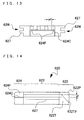
- Fig. 12 is a front view of a cover member constituting the mounting case
- Fig. 13 is a rear view shown from the direction of Z4 shown in Fig. 12
- Fig. 14 is a side view shown from the direction of Z5 shown in Fig. 12.
- the mounting case 601 comprises the plate member 610 and the cover member 620.
- the electro-optical device 500 which is accommodated in the mounting case 601, comprises another optical component such as a reflection preventing plate overlapped with the surface thereof, and an external circuit connecting terminal, to which a flexible connector 501 is connected, in addition to the electro-optical devices shown in Figs. 2 and 3.
- a polarizing plate or a phase difference plate may be provided to the optical system of the liquid crystal projector 1100, or it may be overlapped with the surface of the electro-optical device 500.
- a dustproof substrate 400 is provided to portions not facing the liquid crystal layers 50 in the TFT array substrate 10 and the counter substrate 20 (see Figs. 4 and 7).
- the dustproof substrate 400 is constructed to have a predetermined thickness.
- the dustproof substrate prevents dirt or dust around the electro-optical device 500 from directly attaching on the surface of the electro-optical device. Therefore, it is possible to effectively remove a defect that a figure of dirt or dust appears on the magnified projection image. Since the dustproof substrate 400 has the predetermined thickness, the dustproof substrate has a defocusing function to deviate the focus of the source light or the vicinity thereof from a location where dirt or dust exists, that is, from the surface of the dustproof substrate 400.
- the electro-optical device 500 comprising the TFT array substrate 10, the counter substrate 20, and the dustproof substrate 400 is accommodated in the mounting case 601 comprising the plate member 610 and the cover member 620.
- a molding member 630 is filled between the electro-optical device 500 and the mounting case 601. The molding member 630 ensures bonding between the electro-optical device 500 and the mounting case 601 and also surely prevents the occurrence of dislocation of the former within the latter.
- the light is incident on the cover member 620, passes through the electro-optical device 500, and emits from the plate member 610. That is, referring to Fig. 1, the component facing the dichroic prism 1112 is not the cover member 620 but the plate member 610.
- the plate member 610 is a member having a substantially quadrilateral shape in plan view and is disposed to face one surface of the electro-optical device 500.
- the plate member 610 and the electro-optical device 500 are directly abutted against each other, and the latter is mounted on the former.
- the plate member 610 comprises a window 615, a strength reinforcement portion 614, a bent portion 613, a cover member fixing hole 612, and attaching holes 611 a to 611d and 611e.
- the window 615 is formed in an opening shape in which a portion of the member having the substantially quadrilateral shape is opened.
- the window 615 is a member of enabling light to transmit from the upper side to the lower side in Fig. 6.
- the light transmitted through the electro-optical device 500 can be emitted by the window 615.
- a double coated adhesive tape 1 is provided on the edge of a window 615, i.e., a portion on which the electro-optical device 500 is put.
- Fig. 7 illustrates an arrangement of a double coated adhesive tape 1 as seen in cross-sectional view. See a portion within the circle in Fig. 7.
- a peripheral region located around an image display region 10a in the electro-optical device 500 abuts against the edge of the window 615 such that the electro-optical device 500 and the plate 610 are bonded to each other via the double coated adhesive tape 1.
- the abutting portion between the electro-optical device 500 and the plate member 610 via such a double coated adhesive tape 1 corresponds to an example of 'area contacted portion', as described in the present invention.
- the strength reinforcement portion 614 has a three-dimensional shape formed by a process of convexing a portion of the member having the substantially quadrilateral shape higher than other portions in plan view. In this way, the strength of the plate member 610 is reinforced.
- the strength reinforcement portion 614 may be disposed at a location to substantially abut against one side of the electro-optical device 500 (see Fig. 7). However, strictly speaking, both of them are not abutted against each other in Fig. 7.
- the bent portion 613 is formed such that a part of each of two opposed sides of a generally quadrilateral member forming the appearance of the plate member 610 is bent toward the inside of the quadrilateral shape. Particularly, in the embodiment, as shown in Figs. 9 and 11, the bent portion 613 is bent such that it rises at a right angle from the quadrilateral plate-shaped member.
- the bent portion 613 according to the embodiment is formed in the described manner so that one side thereof faces the outside of the plate member 610 and the other side thereof faces the inside of the plate member 610.
- the outer surface related to the former will be referred to as a first facing surface 613F1 and the inner surface related to the latter will be referred to a second facing surface 613F2 (see Fig. 6).
- a second facing surface 613F2 of the bent portion 613 contacts with the outer surface of the electro-optical device 500 via the molding material 630 at the time of assembling the plate member 610 and the cover member 620 together as shown in Fig. 6.
- the electro-optical device 500 as shown in Fig. 7, extends in left and right directions in Fig. 7 with a predetermined length
- the bent portion 613 extends in left and right directions in Fig. 11 with a predetermined length.
- these Figs. 7 and 11 just overlap each other. For this reason, as shown in Fig.
- Fig. 7 is a cross-sectional view taken along Y-Y' of Fig. 5, they are different from each other, strictly speaking.
- the abutting portion of the embodiment between the second facing surface 613F2 and the side of the electro-optical device 500 corresponds to an example of the 'second abutting portion' referred in the present invention, and corresponds to an example of the 'area contacted portion' referred in the present invention.
- the first facing surface 613F1 of the bent portion 613 is abutted against the inner surface of the cover member 620 when assembling the plate member 610 and the cover member 620 together (see Fig. 6).
- the cover member 620 in particular, the cover main body 623, as shown in Figs. 5 to 8 and Figs. 12 to 14, has a 'lid-free box shape'.
- the cover member 620 as shown in Fig, 6, is provided with a floor portion 62F called a 'floor' in the 'lid-free box shape', and a wall portion 62W called a 'wall' that is erected on the floor portion 62F.
- 'lid-free' means that a portion called a 'ceiling' does not exist.
- the cover member 620 having such a shape, as shown in Fig. 6, is arranged to cover the electro-optical device 500 such that the floor portion 62F faces the surface of a dustproof substrate 400 at the counter substrate 20, which constitutes the electro-optical device 500 (that is, the floor portion 62F is located on the upper side in Figure), and the wall portion 62W faces the side of the electro-optical device 500.
- the cover member 620 according to the embodiment is arranged in such a manner to substantially completely cover the electro-optical device 500, the plate member 610 can serve as a lid for the cover member 620 having the lid-free box shape(see Figs. 5 to 8).
- the first facing surface 613F1 is adapted to abut against the inner surface of the wall portion 62W, i.e., the surface of the wall portion 62W that faces a space surrounded by the wall portion 62W and the floor portion 62F, or a space receiving the electro-optical device 500.
- the plate member 610 and the cover member 620 contact with each other with a comparatively wide contact area therebetween. Further, in the embodiment where such a contact state is employed, the bent portion 613 is located inside the lid-free box shape, which constitutes the cover member 620.
- the abutting porting between the first facing surface 613F1 and the wall portion 62W in this embodiment corresponds to an example of the 'first contacting portion' referred in the present invention.
- the plate member 610 and the cover member 620 according to the embodiment is adapted to be fixed each other using a cover member fixing hole 612 and a convex portion 621. In this case, in a predetermined region where the cover member fixing hole 612 is formed (see Fig.
- a tapered portion 622T where the convex portion 621 is formed i.e., one side of the aforementioned triangular prism introduced for illustrating the tapered portion 622T, the plate member 610 and the cover member 620 abuts against each other. See reference numeral 622F in Fig. 7.
- the 'first abutting portion' referred in the present invention also implies the above-mentioned abutting portion.
- the cover member fixing hole 612 is a hole for engaging with a convex portion 621 provided at the corresponding location in the cover member 620.
- the plate member 610 and the cover member 620 are fixed to each other by engaging the cover member fixing hole portion 612 with the convex portion 621.
- the cover member fixing hole 612 comprises two holes as shown in each figure. In case of need of distinguishing the holes, the two holes are referred to as cover member fixing holes 612a and 612b, respectively.
- the convex portion 621 comprises two convex portions. In case of need of distinguishing the convex portions, the two convex portions are referred to as convex portions 621a and 621b, respectively.
- the attaching holes 611a to 611d are used for attaching the electro-optical device encased in the mounting case within the liquid crystal projector 1100 as shown in Fig. 1.
- the attaching holes 611a to 611d are provided to four corners of the member having the substantially quadrilateral shape.
- an attaching hole 611e is provided in the embodiment.
- the attaching hole 611e is disposed to form a triangle together with the attaching holes 611c and 611d of the attaching holes 611a to 611d.
- the attaching holes 611e, 611c, and 611d are disposed at the corresponding apexes of the triangle. In this manner, in the embodiment, it is possible to fix the four points at the four corners using the attaching holes 611a to 611d and to fix the three points at the three corners using the attaching holes 611e, 611c, and 611d.
- the plate member 610 has the following features. That is, the plate member 610 according to the embodiment is made of a material having a coefficient of linear expansion within a predetermined range, preferably, ⁇ 5 ⁇ 10 -6 /°C, and more preferably ⁇ 2.5 ⁇ 10 -6 /°C, using as a reference a coefficient of linear expansion of the counter substrate 20 and the TFT array substrate 10, which constitutes the electro-optical device.
- the counter substrate 20 and the TFT array substrate 10, or the aforementioned dustproof substrate 400 (hereinafter, referred to as 'TFT array substrate, etc.') is made of, for example, quarts glass, and the plate member 610 is made of, for example, so-called invar alloy (for example, 36NI-Fe alloy).
- invar alloy for example, 36NI-Fe alloy
- the cover member 620 is a member having substantially cube shape, and is arranged to face the surface opposite to the surface facing the plate member 610 in the electro-optical device.
- the cover member 620 is preferably made of light shielding resin, metallic material, and the like in order to prevent the leakage of the light in the peripheral region of the electro-optical device 500 and the introduction of the stray light from the peripheral region to the image display region 10a. Since it is preferable that the cover member 620 should function as a heat sink for the plate member 610 or the electro-optical device 500, the cover member 620 is preferably made of materials of relatively high heat conductivity, such as aluminum, magnesium, copper, or an alloy thereof.
- the convex portion 621 is formed in the cover member 620.
- the convex portion 621 is used for fixing the plate member 610, and comprises two convex portions 621a and 621b at the locations corresponding to the cover member fixing holes 612a and 612b.
- the convex portion 621 according to the embodiment is provided to form a portion of the cooling air introducing portion 622 or a tapered portion 622T as described later.
- the cover member 620 has a cooling air introducing portion 622, a cover main body 623, and the cooling air discharging portion 624 in more detail.
- all these three portions 622, 623, and 624 are integrally formed.
- the cooling air introducing portion 622 as shown well in Fig. 4, Fig. 5, Fig. 7, Fig. 12, or Fig. 14, comprises the tapered portion 622T and the baffle plate 622P, which constitute an example of the 'cooling air scattering prevention portion' or the 'cooling air introducing portion', respectively, referred in the present invention.
- the tapered portion 622T constituting an example of the 'slope portion' referred in the present invention generally has an appearance such as a triangular prism whose bottom face is a right-angled triangle.
- the tapered portion 622T has an appearance where one side of the triangular prism in the tapered portion is attached on the one side of the cover main body 623.
- the one side of the triangular prism comprises a side interposed between a rectangular portion of the bottom of the triangular prism and a corner portion adjacent thereto.
- the tapered portion 622T has a shape comprising a root portion 622T1 with a height largest at the side of the cover main body 623 and a tip 622T2 with a height gradually lowered therefrom.
- the term 'height' is a distance in the up-down direction in Fig. 7.
- a doted line extending in the up-down direction is represented as a reference.
- the tapered portion 622T having such a shape can be provided in a 'pointed shape'.
- the cover member 620 including the tapered portion 622T having such a pointed shape is arranged such that the tip 622T2 constituting a part of the pointed shape faces the flow of cooling air. See Fig. 15 and the description related thereto, which will be described later.
- the baffle plate 622P has a shape of a wall erected along one side between two apexes except for the right angle apexes on the bottom of the triangular prism.
- the height of the baffle plate 622P is constant at any place between the root portion 622T1 and the tip 622T2 although the height of the tapered portion 622T is gradually lowered from the root portion 622T1 to the tip 622T2.
- the baffle plate 622P arranged as descibed above can be formed to surround one side 622TF of the tapered portin 622T from both sides (see Fig. 4).
- the side 622TF is an example of the side, which is typically assumed as the 'surface constituting a slope portion' referred in the present invention.
- the cover main body 623 which is a member having a substantially rectangular parallelepiped shape, is interposed between the cooling air introducing portion 622 and the cooling air discharging portion 624 as shown in Figs. 4 to 8 and Figs. 12 to 14.
- the cover main body 623 is a member having a shape of a box without its cover.
- the 'cover' in this expression may be considered to correspond to the plate member 610 described above.
- the cover main body 623 includes the window 625 and the side fin portion 627.
- the side fin portion 627 corresponds to an example of the 'surface area increasing portion' or the 'fin' , referred in the present invention.
- the window 625 whose bottom plane having the box shape and a top surface in Fig. 4 or 6 are formed in an opening shape is a member of capable of penetrating the light from the upper part to the lower part in Fig. 6.
- the light emitted from the lamp unit 1102 within the liquid crystal projector 1100 shown in Fig. 1 can be incident to the electro-optical device 500 through the window 625.
- the edge of the window 625 has a tapered shape, as well shown in Fig. 7.
- the side 622TF in the tapered portion 622T and the surface 500F of the electro-optical device 500 on the upper side in Fig. 7 are adapted to be 'continuous'.
- the side 622TF intersects the surface 623F of the cover main body 623 on the upper side in Fig. 7 where the window 625 is formed, at an angle that is not a right angle.
- the surface 623F intersects the surface 625F constituting the tapered shape of the edge of the window 625, at an angle that is not right angle.
- the surface 625F also intersects the surfae 500F at an angle that is not right angle.
- the peripheral region near the image display region 10a in the electro-optical device 500 may be preferably formed to abut against the edge of the window 625 similarly to the description of the window 615 in the plate member 610 (see Fig. 7).
- the cover main body 623, more particularly, the edge of the window 625 can also hold the electro-optical device 500.
- a double coated adhesive tape 2 is also provided at the edge of the window 625 of the cover member 620 in the similar way. See a portion inside the circle in Fig. 7.
- the cover member 620 and the electro-optical device 500 are also bonded to each other via the double coated adhesive tape 2. Further, these cover member 620 and electro-optical device 500 have the 'area contacted portion', referred in the present invention, in a region where the double coated adhesive tape 2 exists.
- Both the double coated adhesive tape 2 and the double coated adhesive tape 1 provided at the edge of the window 615 of the plate member 610 has a rectangular shape to surround the whole edges of the windows 615 and 625, in other words, apertures of the windows 615 and 625.
- the double coated adhesive tapes 1 and 2 can be provided so as to correspond the whole region in the peripheral region of the electro-optical device 500.
- the double coated adhesive tapes 1 and 2 have particularly the following features. That is, firstly, the double coated adhesive tapes 1 and 2 are made of a material having a heat conductivity of 0.6 or more W/m ⁇ K, and more preferably, 1.0 or more W/m ⁇ K.
- double coated adhesive tapes satisfying these conditions may comprise a double coated adhesive tape including heat conductive silicon rubber, and a double coated adhesive tape employing a multiplayer structure in which different materials including heat-conductive silicon rubber are used for an adhesive layer and a layer to be bonded, and comprises an acryl-based heat-conductive double coated adhesive tape mainly including acryl rubber, and including metal oxide or metal nitride, etc., in addition thereto.
- 'Ehuco TM sheet' manufactured by Ehuco Co., Ltd. or 'TCATT heat-conductive adhesive transfer tape' (Product Nos. 9882, 9885, and 9890) manufactured by Sumitomo 3M Co. Ltd., etc. are marketed and these are available.
- the side fin portion 627 is formed at both sides of the cover main body 623.
- the term 'both sides' is the sides except for the sides where the aforementioned cooling air introducing portion 622 and the cooling air discharging portion 624 are provided.
- the both sides (hereinafter, sometimes referred to as a 'sidewall portion 62W'), for example, face one side of the electro-optical device 500 and the other side facing the one side, respectively, as shown in Fig. 6, etc.
- the inner surface of the sidewall portion 62W is abutted against the outer surface of the bent portion 613 in the plate member 610 at the process of assembling the cover member 620 and the plate member 610 together (see Fig. 6).
- the sidewall portion 62W according to the embodiment may face the one side and the other side of the electro-optical device 500, in particular, through the bent portion 613.
- the side fin portion 627 has a shape of a plurality of portions straightly protruding from the side in parallel from the cooling air introducing portion 622 to the cooling air discharging portion 624 as shown in Fig. 4 or Figs. 6 and 13.
- two columns of straight fins are disposed in parallel.
- the presence of the side fin portion 627 leads to the increase of the surface area of cover main body 623 or the cover member 620.
- the side fin portion 627 is formed with sidewall portion 62W having a relatively large ratio of occupation over the entire cover member 620, the increase of the surface area is effectively obtained.
- the gap g1 (see Fig. 14) between two columns of linear fins consitituting the side fin portion 627 may be set to 1 mm or more.
- the side fin portion 627 having the aforementioned shape may be formed by a process such as, for example, a cutting process, a forging process, a pressing process, an injection molding process, or a casting process, at the same time of or after the process of forming the cover member 620. According to these processes, it is possible to easily form the side fin portion 627.
- the cooling air discharging portion 624 comprises a flexible connector leading portion 624C and a rear fin portion 624F as shown in Figs. 4, 5, 8, 12, or 13.
- the flexible connector leading portion 624C is provided on one side of the cooling air discharging portion to face the side of the cover main body 623 on which the tapered portion 622T is provided. More specifically, a member having a cross-sectional shape of 'u' on the aforementioned side is attached by an aperture having a cross-sectional shape of 'u' in the downward direction of Fig. 8 or 13 as shown in Fig. 8 or 13.
- a flexible connector 501 connected to the electro-optical device 500 is drawn out from the space in a shape of 'u'.
- the rear fin portion 624F corresponding to an example of the 'surface area increasing portion' or the 'fin' referred in the present invention is provided on the ceiling plate having a U-shaped section in the flexible connector leading portion 624C. More specifically, the rear fin portion 624F has a shape of a plurality of portions straightly protruding from the sealing plate in parallel to correspond to the reference numerals in a direction of straightly protruding portions, that is, the side fin portions 627 to be described later, as shown in Fig. 4, 5, 8, 12, or 13. In the embodiment, particularly, the rear fin portion 624F, as shown in the above respective figures, includes four juxtaposed linear fins. Meanwhile, these four fins are formed to comply with the flow of cooling air.
- the gap g2 (see Fig. 8 and Fig. 13) between the four linear fins is set to be 1 mm or more.
- the rear fin portion 624F of this arrangement allows the surface area of the cooling air discharging portion 624 or the cover member 620 to be increased.
- the rear fin portion 624F having the aforementioned shape may be formed by a process such as, for example, a cutting process, a forging process, a pressing process, an injection molding process, or a casting process, at the same time of or after the process of forming the cover member 620. According to the above method, the side fin portion 624F can be comparatively easily formed.
- the gap g2 between four linear fins constituting the rear fin portion 624F is set to be 1 mm or more as described above. That is, for example, a linear fin located at the leftmost position in Fig. 15 and a fin located at the next right position thereof have a gap of 1 mm or more therebetween, and the next right fin and a fin located at the further next right position thereof have a gap of 1 mm or more, and so on.
- the ' first column of fins' and the ' second column of fins' referred in the present invention for example, means a fin located at the leftmost position and the next right fin thereof, or the next right fin and the further next right fin thereof.
- the 'first column of fins' and the 'second column of fins' referred in the present invention are generally adapted irrespective of the number of columns of fins actually provided. Meanwhile, the 'first column of fins' and the 'second column of fins' have a concept which can be also applied to two columns of linear fins constituting the side fin portion 627.
- dimples to give depressions to the surface of the cover member 620, thereby increasing the surface area thereof, instead of the fins or in addition to the fins.
- Fig. 15 is a perspective view of an electro-optical device encased in a mounting case and illustrates a typical 'heat transfer path' in the electro-optical device encased in a mounting case.
- Fig. 16 is a partially enlarged view of Fig. 6, and an explanatory view illustrating a heat transfer behavior through a bent portion.
- the illustration of elements as well as the window will be appropriately omitted in Fig. 15 in order to clearly show the 'heat transfer path'.
- the electro-optical device 500 is irradiated with intense light from a lamp unit 1102 within the liquid crystal projector 1100, and thereby the temperature thereof gradually rises.
- the 'heat transfer path' reaching the cover member 620 from the electro-optical device 500 via the plate member 610 is formed, thereby achieving the cooling of the electro-optical device 500.
- a heat transfer path HR1 reaching the cover member 620 from the electro-optical device 500 via the bent portion 613 of the plate member 610 secondly, a heat transfer path HR2 reaching the tapered portion 622T of the cooling air introducing portion 622 from the electro-optical device 500 via the double coated adhesive tape 1, and thirdly, a heat transfer path HR3 directly reaching the cover 620 from the electro-optical device 500 via the double coated adhesive tape 2 (herein, the tape 2 is not shown in Fig. 15. See Fig. 4, Fig. 7, etc.).
- a portion located on the way of the heat transfer paths HR1 and HR2 shown in Fig. 15 and indicated by thick line means that heat is conducted through the plate member 610 in the related portion.
- the heat transfer path HR1 will be described.
- this heat transfer path HR1 it is possible to effectively achieve the cooling of the electro-optical device 500 thanks to the presence of the bent portion 613.
- the outer surface of the electro-optical device 500 contacts the second facing surface 613F2 of the bent portion 613 via the molding material 630, the first facing surface 613F1 as the rear face of the second facing surface 613F2 contacts the inner face of the wall portion 62W of the cover member 620.
- Heat generated in the electro-optical device 500 is sequentially transferred to the bent portion 613 and cover member 620, in other words, the plate member 610 and cover member 620 function as a heat sink of the electro-optical device 500, thereby effectively cooling the electro-optical device 500.
- such heat transfer via the bent portion 613 or the heat transfer path HR1 has the following features.
- the 'first abutting portion' referred in the present invention includes a region where the cover member fixing hole 612 and the convex portion 621 other than the bent portion 613 and the wall portion 62F. That is, the heat transfer from the plate member 610 to the cover member 620 occurs even in the above region.
- the thickness of the bent portion i.e., the distance between the first facing surface 613F1 and the second facing surface 613F2 is comparatively small (see Fig. 13 and Fig. 6). Accordingly, since the flow of heat reaching the wall portion 62W from the electro-optical device 500 via the bent portion 613is performed without stagnation, the cooling of the electro-optical device 500 is greatly promoted. Meanwhile, the thickness of the plate member 610 and the bent portion 613 may be set to be, for example, 0.2 to 0.8 mm from the above-mentioned viewpoint or from the viewpoint of the strength which the plate member 610 should have.
- the heat transfer paths HR2 and HR3 will be described.
- the double coated adhesive tapes 1 and 2 are made of a material having a high heat conductivity as described above, thereby efficiently performing the heat transfer from the electro-optical device 500 to the plate member 610, or the heat transfer from the electro-optical device 500 to the cover member 620.
- the double coated adhesive tapes 1 and 2 have a rectangular shape and a comparatively broad area, i.e., the electro-optical device 500, the plate member 610, and the cover member 620 have an area-contacted portion, respectively, the working effects related to the above heat transfer is further promoted.
- the heat transfer from the electro-optical device 500 to the cover member 620 is performed without passing through the plate member 610.
- the 'heat transfer path' referred in the present invention includes such a heat transfer path HR3.
- the heat transfer paths HR1, HR2, and HR3 as shown in Fig. 15 simply show a typical implementation of flow of heat, respectively.
- the various heat transfer paths can be implemented using the electro-optical device 500 as a starting point other than the heat transfer paths shown in FIG. 15. For example, as also shown in Fig.
- a heat transfer path reaching the bent portion 613 from the electro-optical device 500 via the double coated adhesive tape 1 and further reaching the wall portion 62W from the bent portion can be considered.
- the molding material 630 does not exist in such a heat transfer path, it is possible to effectively achieve the heat transfer from the electro-optical device 500 to the cover member 620 via the plate member 610 even in an aspect (for example, see Fig. 22) which implements the fixation of the electro-optical device 500 by the plate member 610 without using the molding material 630.
- the electro-optical device encased in a mounting case according to the embodiment it is possible to absorb heat from the electro-optical device 500, i.e., to effectively achieve the cooling of the electro-optical device 500 by the heat transfer paths HR1, HR2, and HR3 as shown in Fig. 15. Accordingly, according to the present invention, it is possible to effectively prevent the temperature of the electro-optical device 500 from rising, to prevent, for example, the characteristics of the liquid crystal layer 50 from deteriorating, or to prevent a so-called hot spot from being created in the liquid crystal layer 50. As a result, it is possible to display high quality images.
- the electro-optical device 500 can be effectively cooled as described above.
- the temperature of the plate member 610 rises as time lapses. Accordingly, the plate member 610 thermally expands. Since the plate member 610 functions as a member to fix the electro-optical device 500 (see later description), this may cause the dislocation of the electro-optical device 500 in the mounting case 601.
- the thermal capacity of the plate member 610 and or the thermal capacity of the cover member 620 there is a limit to the thermal capacity of the plate member 610 and or the thermal capacity of the cover member 620, and when the absorption of heat the above-mentioned from electro-optical device 500 continues, the thermal capacity thereof may be logically saturated before long. As a result, the plate member 610 and the cover member 620 may not function as a heat sink sufficiently.
- the plate member 610 since the plate member 610 according to the embodiment is made of a material having a coefficent of linear expansion within predetermined range, using as a reference a coefficent of linear expansion of the TFT array substrate 10, etc., constituting the electro-optical device 500. According to the aforementioned example, the plate member 610 is made of, for example, invar alloy, and the TFT array substrate 10, etc., is made of quarts glass. As a result, the first problem is effectively solved.
- the cover member 620 comprises the cooling air introducing portion 622, the side fin portion 627, the cooling air discharging portion 624, the rear fin portion 624F, etc., thereby effectively solving the second problem.
- Fig. 17 is a perspective view of an electro-optical device encased in the mounting case and illustrates a typical flow of a wind into the electro-optical device encased in the mounting case.
- the cover member 620 Since the cover member 620 has the aforementioned construction, the wind blown from the sirocco fan 1300 provided in the liquid crystal projector 1100 as shown in Fig. 1 is flowing near the mounting case 601 or the cover member 620 as shown in Fig. 17.
- cooling air is blown to the cover main body 623 to which the surface 500F of the electro-optical device 500 is exposed, as if it runs up the tapered portion 622T of the cooling air introducing portion 622 (see reference numeral W1).
- the tapered portion 622T, or the tip 622T2 as a part constituting the tapered portion does not exist, and if it is supposed that, for example, a block-shaped member 622X having a predetermined thickness exists instead of the tapered portion 622T, as shown in Fig. 18 as a comparative figure of Fig.
- the cover member 620 has the tapered portion 622T. As a result, it is possible to efficiently blow cooling air toward the cover member 623.
- the baffle plate 622P is provided to the cooling air introducing portion 622, the cooling air blown in any direction can be almost guided on the tapered portion 622T, and moreover, into the cover main body 623 (see symbol W2 in Fig. 17).
- the embodiment it is possible to efficiently blow cooling air toward the cover main body 623 by allowing the baffle plate 622P to collect cooling air efficienly.
- the sirocco fan 1300 an example of the cooling air discharging portion provided to the liquid crystal projector 1100 provides a whirlpool wind as already described above (see Fig. 1). Accordingly, in the electro-optical device encased in a mouting case, there is a possibility that the cooling air W2 blown in an irregular way as shown in Fig. 17 may be comparatively much observed. However, in the embodiment, it is possible to efficiently blow even the cooling air W2 blown in such an irregular way toward the cover main body 623 by forming the baffle plate 622P. Moreover, in the embodiment, since the baffle plate 622P is formed to surround the side 622TF of the tapered portion 622T along which cooling air runs up, the blowing of cooling air toward the cover main body 623 is more effectively performed.
- the cooling air passing through the cooling air introducing portion 622 in the above manner reaches the cover main body 623. Since the cover main body 623 accommodates the electro-optical device 500, and the surface 500F of the electro-optical device 500 is exposed to the outside through the window 625, the cooling air blown into as described above cools the electro-optical device 500 itself efficiently. Moreover, in the embodiment, particularly, by forming the edge of the window 625 in a tapered shape, the surface 500F of the electro-optical device 500 and the side 622TF of the tapered portion 622T are formed successively, thereby allowing the cooling effect of the electro-optical device 500 to be more efficient. That is, as indicated in Fig.
- the cooling air which has ran up the side 622TF of the tapered portion 622T, is blown out of the surface 623F of the cover main body 623 formed in the window 625 and out of the surface 625F constituting the edge of the window 625 (see Fig. 7 for both of them) without its running being disturbed.
- the cooling air can flow into the surface 500F of the electro-optical device 500 (see reference numeral W1' in Fig. 17).
- the cooling air which has past through the cooling air introducing portion 622, cools the cover main body 623 or the cover member 620 as well as the above-mentioned electro-optical device 500 itself.
- the cover main body 623 is provided with the side fin portion 627, the cover main body 623 or the cover member 620, or the electro-optical device 500 can be more efficiently cooled thanks to the surface area increasing effect of the side fin portion.
- the cooling air which has past the cover main body 623, next, reaches the cooling air discharging portion 624.
- the rear fin portion 624F is formed in the cooling air discharging portion 624 as described above. Since the rear fin portion 624F has straight fins and the surface area of the cooling air discharging portion 624 is increased as described above, it is possible to effectively cool the cooling air discharging portion 624 and the cover member 620. Moreover, in the embodiment, since the linear fins are formed to comply with the flow of cooling air, and the gap g2 between these linear fins is set to be 1 mm or more, the following working effects can be achieved.
- the rear fin portion 624F since the rear fin portion 624F is formed to comply with the flow of cooling air, the rear fin portion 624F can naturally conduct the cooling air back to back without excessively obstructing the flow of the cooling air (see reference numeral W1' in Fig. 17). Accordingly, according to the embodiment, the cooling effect of the cover member 620 caused by the rear fin portion 624F can be effectively obtained.
- the cooling air flows in a direction, which is not necessarily complied with the extending direction of the straight fins.
- the sirocco fan 1300 provided to the liquid crystal projector 1100 supplies a whirlpool wind as already described above (see Fig. 1). Therefore, strictly speaking, the direction of the cooling air is not always the straight direction toward the electro-optical device encased in the mounting case, which is the light valve 100R, 100G, or 100B.
- the embodiment belongs to the case that it is provided 'to comply with the flow of the cooling air' referred in the present invention. This is because even in aforementioned situation, most of the cooling air shown in Fig. 17 flows into the cooling air introducing portion 622, the cover main body 623, and cooling air discharging portion 624 in this order.
- the construction that 'the fins are provided to comply with the flow of the cooling air' according to the present invention does not mean only the case that the fins are provided to strictly or completely comply with the flow of the cooling air. As described above, it also includes the case where the fins are provided to roughly comply with the direction of the flow of the cooling air based on the electro-optical device encased in the mounting case.
- the gap g2 between linear fins constituting the rear fin portion 624F is set to be 1 mm or more, the cooling air W1' as shown in Fig. 17 can easily flow between the linear fins, even though the static pressure of the cooling air W1' is low and the air quantity thereof is small.
- the electro-optical device encased in the mounting case is provided as the light valves 100R, 100G, and 100B of the liquid crystal projector 1100 as shown in Fig. 1.
- the other components such as the incident lens 1122 and the relay lens 1123 need to be provided, so that the electro-optical device encased in the mounting case, that is, the light valves 100R, 100G, and 100B, and the sirocco fan 1300 have to be disposed with a relatively long distance. And thus, in some cases, it is difficult to dispose both of them to completely be opposite to each other. In this case, it is considered that only the cooling air having a low static pressure and a low amount are blown to the electro-optical device encased in the mounting case.
- the gap g2 between the aforementioned linear fins is comparatively largely set to be 1 mm or more, it is possible to make the aforementioned cooling air having a low static pressure and a small quantity of air blown out even in the gap g2. By doing so, since the surface area of the fins that are exposed to the cooling air is increased, the characteristics on the heat dissipation of the fins can be more improved. Therefore, according to the embodiment, it is possible to further improve the capability of the heat dissipation of the overall cover member 620.
- the above working effects can be enjoyed in generally similar way, even in case that the gap g1 between two columns of linear fins constituting the side fin portion 627 is set to be 1 mm or more.
- the cover member 620 is generally adapted to achieve the effective cooling in the whole cover member 620. According to this, it is meant the flow of heat from the electro-optical device 500 via the bent portion 613 to the plate portion 610 or the cover member 620, which has been described with reference to Fig. 15, is always effectively maintained. In other words, since the cover member 620 is suitably cooled in a normal state, its function as a heat sink can be maintained at any time, and thus, the heat dissipation for the cover member 620, from the plate member 610 and moreover, from the electro-optical device 500 can be effectively performed. In addition to this, if the cover member 620 in the embodiment is made up of a material having relatively high heat conductivity such as aluminum, magnesium, copper, or alloys thereof as described above, the aforementioned function and effect will be more effectively improved.
- Fig. 19 and Fig. 20 have a purpose similar to that of the figure Fig. 12 and Fig. 14, respectively, and illustrate a different aspect of fins formed in the side wall portion 62W.
- the side wall portion 62W of the cover main body 623 is formed with a side fin portion 628 consisting of a plurality of small fins arranged in zigzags. More specifically, the side fin portion 628 comprises six small fins for every side of the cover main body 623, that is, twelve small fins for the overall cover member 620. Referring to the only one side, the side fin portion 628 comprises, for example, a first column of fins and a second column of fins, which are in the left and right directions in the figure, respectively, as shown in Fig. 20. In addition, the first column of fins comprises three small fins 1(1), 1(2), and 1(3), and the second column of fins comprises three small fins 2(1), 2(2), and 2(3).
- the presence of the heat transfer paths HR1, HR2, and HR3 connecting the electro-optical device 500 with the cover member 620, the effective cooling of the cover member 620, etc. allows the effective cooling of the electro-optical device 500 to be achieved.
- the cover member 620 may accumulate heat excessively.
- the cover member 620 employs an aspect made of a high heat conductivity of material such as aluminum as described above in order to further raise the heat conductivity in the cover member 620 itself, it shall be considered that the cover member 620 theremally expands comparatively largely because such material may often comprise a comparatively large coefficent of linear expansion of material.
- the cover member 620 mainly shares a function to cool the electro-optical device 500
- the plate member 610 mainly shares a function to prevent any dislocation of the electro-optical device 500 in the mounting case 601.
- the plate member 610 is provided with, as means for fixing the electro-optical device 500, the bent portion 613, the strength reinforcement portion 614, and the double coated adhesive tape 1. That is, firstly, according to the bent portion 613, the second facing surface 613F2 of the bent portion 613 abuts against the outer surface of the electro-optical device 500, thereby constraining the installation position of the electro-optical device 500 to some degree.
- the bent portion 613 is formed such that a part of each of two opposed sides of a generally quadrilateral shape forming a schematic feature of the plate member 610 is bent toward the inside of the quadrilateral shape.
- the contact area between the plate member 610 and the electro-optical device 500 is comparatively increased, and the electro-optical device 500 can be comparatively stably located on the plate member 610, it is possible to obtain the working effect of positioning the electro-optical device by the plate member.
- the strength reinforcement portion 64 is formed as if it substantially contacts with one side of the electro-optical device 500, according to the strength reinforcement portion 614, the installation position of the electro-optical device 500 is constrained to some degree.
- the adhesiveness with the double coated adhesive tape 1 constrains the installation position of the electro-optical device 500.
- the plate member 610 carries a function to prevent any dislocation of the electro-optical device 500 in the mounting case 601.
- the cover member 620 according to the embodiment is constructed to have a function to prevent any dislocation of the electro-optical device 500, large thermal expansion of the cover member 620 causes the electro-optical device 500 to be displaced. Thus, there is a high possibility of causing any dislocaiton of the electro-optical device 500 in the mounting case 601.
- the role sharing between the plate member 610 and the cover member 620 is achieved as described, the above-mentioned inconvenience does not occur. That is, since the cover member 620 mainly does not carry a function to fix the electro-optical device 500, comparatively free heat deformation is allowed. Further, since the plate member 610 mainly does not carry a function to cool an electro-optical device, it is possible to make the plate member carry a function to fix an electro-optical device more safely.
- a construction for fixing the electro-optical device 500 by the plate member 610 any construction other than the above-mentioned one can be employed.
- a fixing construction as shown, for example, in Fig. 21 and Fig. 22, can be employed.
- Fig. 21 is a plan view, for the purpose similar to that of Fig. 9, of the front of the plate member 610, illustrating a construction in which the plate member 610 and the electro-optical device 500 installed in the plate member 610 are fixed to each other using photo-curing resin therebetween.
- Fig. 22 is a sectional view, for the purpose similar to that of Fig.
- FIG. 22 is a cross-sectional view taken along the line X2-X2' (see Fig. 21) different from the line X1-X1' of Fig. 5.
- FIG. 21 it may considered that the contour of the molding material 1' corresponds to that of the electro-optical device 500).
- the double coated adhesive tape 1 and the molding material 1' can be substituted mutually. Meanwhile, this is applied to the double coated adhesive tape 2 (see Fig. 5 and Fig. 7), in other words, molding material (not shown) may be provided instead of the double coated adhesive tape 2.
- photo-curing resin 5 is provided between the side of electro-optical device 500, and a surface, which faces one surface of the electro-optical device 500 in the plate member 610. More specifically, the photo-curing resin 5 is provided to correspond to four corners of the electro-optical device 500. Further, in each of these four corners, the photo-curing resin 5 is located between the above mentioned surfaces of the electro-optical device 500 and the plate member 610, and the inner surface of the bent portion 613, i.e., the second facing surface 613F2 of the bent portion 613.
- the electro-optical device 500 is constrained with the bent portion 613, the strength reinforcement portion 614, etc., and is fixed with the molding material 1' or the photo-curing resin 5 which can exhibit a comparatively strong fixing effect. Accordingly, according to the embodiment, it is possible to obtain a fixing effect to the same degree as or greater degree than that of the aforementioned fixing construction. Moreover, in Fig. 21, particularly, although the photo-curing resin 5 is provided to correspond to the four corners of the electro-optical device 500, the amount of consumption of the photo-curing resin can be saved, and the electro-optical device 500 can be uniformly fixed.
- the photo-curing resin 5 exhibiting comparatively strong fixing effect is provided.
- the molding material 630 which has been provided hitherto, is not necessarily required. Accordingly, the provision of the molding material 630 can be omitted as shown in Fig. 22.
- the present invention is not limited to the aforementioned embodiments, but it can be modified without departing from the scope of the present invention obtained by the claims and the teachings of the specification and the accompanying drawings.
- the modified electro-optical device encased in the mounting cases, projection display apparatuses, and mounting cases also belong to the technical scope of the present invention.
- the electro-optical device includes an electrophoresis apparatus, an electroluminescent apparatus, a plasma display apparatus, and an apparatus such as a field emission display apparatus, and a surface-conduction electron-emitter display apparatus using an electron-emitting device as well as a liquid crystal panel.
Landscapes
- Physics & Mathematics (AREA)
- Nonlinear Science (AREA)
- General Physics & Mathematics (AREA)
- Chemical & Material Sciences (AREA)
- Mathematical Physics (AREA)
- Crystallography & Structural Chemistry (AREA)
- Optics & Photonics (AREA)
- Signal Processing (AREA)
- Engineering & Computer Science (AREA)
- Multimedia (AREA)
- Liquid Crystal (AREA)
- Devices For Indicating Variable Information By Combining Individual Elements (AREA)
- Projection Apparatus (AREA)
- Photovoltaic Devices (AREA)
Applications Claiming Priority (2)
| Application Number | Priority Date | Filing Date | Title |
|---|---|---|---|
| JP2002370068 | 2002-12-20 | ||
| JP2002370068A JP3736522B2 (ja) | 2002-12-20 | 2002-12-20 | 実装ケース入り電気光学装置及び投射型表示装置並びに実装ケース |
Publications (2)
| Publication Number | Publication Date |
|---|---|
| EP1434081A2 true EP1434081A2 (de) | 2004-06-30 |
| EP1434081A3 EP1434081A3 (de) | 2004-10-06 |
Family
ID=32463489
Family Applications (1)
| Application Number | Title | Priority Date | Filing Date |
|---|---|---|---|
| EP03257790A Withdrawn EP1434081A3 (de) | 2002-12-20 | 2003-12-11 | In Einbaugehäuse eingeschlossene elektrooptische Vorrichtung, Projektionsanzeigegerät und Einbaugehäuse |
Country Status (6)
| Country | Link |
|---|---|
| US (1) | US6950308B2 (de) |
| EP (1) | EP1434081A3 (de) |
| JP (1) | JP3736522B2 (de) |
| KR (2) | KR100625760B1 (de) |
| CN (2) | CN1287196C (de) |
| TW (1) | TWI257594B (de) |
Families Citing this family (24)
| Publication number | Priority date | Publication date | Assignee | Title |
|---|---|---|---|---|
| JP3707470B2 (ja) * | 2002-12-20 | 2005-10-19 | セイコーエプソン株式会社 | 実装ケース入り電気光学装置及び投射型表示装置 |
| JP3698139B2 (ja) * | 2002-12-20 | 2005-09-21 | セイコーエプソン株式会社 | 実装ケース入り電気光学装置及び投射型表示装置並びに実装ケース |
| JP3722141B2 (ja) * | 2002-12-20 | 2005-11-30 | セイコーエプソン株式会社 | 実装ケース入り電気光学装置及び投射型表示装置並びに実装ケース |
| JP3698147B2 (ja) * | 2003-04-22 | 2005-09-21 | セイコーエプソン株式会社 | 実装ケース入り電気光学装置及び投射型表示装置並びに実装ケース |
| JP3707480B2 (ja) * | 2003-04-22 | 2005-10-19 | セイコーエプソン株式会社 | 実装ケース入り電気光学装置及び投射型表示装置並びに実装ケース |
| US7397067B2 (en) | 2003-12-31 | 2008-07-08 | Intel Corporation | Microdisplay packaging system |
| JP2006171566A (ja) | 2004-12-17 | 2006-06-29 | Seiko Epson Corp | 電気光学装置用実装ケース及びその製造方法、電気光学装置、並びに電子機器 |
| JP2006258883A (ja) * | 2005-03-15 | 2006-09-28 | Seiko Epson Corp | 電気光学装置、電気光学装置の製造方法 |
| KR20060107150A (ko) * | 2005-04-07 | 2006-10-13 | 삼성에스디아이 주식회사 | 냉각수단을 구비한 영상표시장치 |
| KR20080033000A (ko) * | 2006-10-12 | 2008-04-16 | 삼성전자주식회사 | 액정표시장치용 렌즈 및 이를 구비한 백라이트 유닛과액정표시장치 |
| KR101303892B1 (ko) * | 2006-11-03 | 2013-09-05 | 삼성디스플레이 주식회사 | 백라이트 어셈블리 및 이를 구비한 액정표시장치 |
| CN101373962A (zh) * | 2007-08-21 | 2009-02-25 | 鸿富锦精密工业(深圳)有限公司 | 电子装置 |
| KR200450690Y1 (ko) | 2008-09-22 | 2010-10-22 | 광성전기산업(주) | 조명 방향 변경 가능한 ac led 내장형 매입등 |
| JP5487704B2 (ja) * | 2009-04-27 | 2014-05-07 | セイコーエプソン株式会社 | 電気光学装置及び電子機器 |
| JP5533001B2 (ja) * | 2010-02-16 | 2014-06-25 | セイコーエプソン株式会社 | 電気光学装置及び電子機器 |
| US20110199328A1 (en) * | 2010-02-18 | 2011-08-18 | Flextronics Ap, Llc | Touch screen system with acoustic and capacitive sensing |
| JP5651984B2 (ja) * | 2010-04-01 | 2015-01-14 | セイコーエプソン株式会社 | 光学装置および電子機器 |
| KR20120071751A (ko) * | 2010-12-23 | 2012-07-03 | 엘지디스플레이 주식회사 | 디스플레이 장치 |
| JP5664979B2 (ja) | 2011-11-04 | 2015-02-04 | 株式会社リコー | 画像投影装置 |
| JP5306511B1 (ja) * | 2012-04-27 | 2013-10-02 | 株式会社東芝 | 電子機器 |
| JP6263992B2 (ja) | 2013-11-29 | 2018-01-24 | セイコーエプソン株式会社 | 電気光学モジュールおよび投射型表示装置 |
| US9684197B2 (en) * | 2013-12-10 | 2017-06-20 | Seiko Epson Corporation | Electro-optic device and electronic apparatus |
| JP6604745B2 (ja) * | 2015-05-15 | 2019-11-13 | キヤノン株式会社 | 光変調素子ユニットおよび画像投射装置 |
| JP6361939B2 (ja) * | 2016-03-08 | 2018-07-25 | パナソニックIpマネジメント株式会社 | 表示装置 |
Citations (3)
| Publication number | Priority date | Publication date | Assignee | Title |
|---|---|---|---|---|
| US5835179A (en) * | 1996-08-30 | 1998-11-10 | Sony Corporation | Liquid crystal display |
| US6056407A (en) * | 1996-12-18 | 2000-05-02 | Seiko Epson Corporation | Projection display device |
| US6414781B1 (en) * | 1999-03-30 | 2002-07-02 | Seiko Epson Corporation | Electro-optical device and projection display device including the same |
Family Cites Families (28)
| Publication number | Priority date | Publication date | Assignee | Title |
|---|---|---|---|---|
| JP2834798B2 (ja) | 1989-11-07 | 1998-12-14 | 三洋電機株式会社 | 反射型投影装置 |
| JPH04125538A (ja) | 1990-09-17 | 1992-04-27 | Pioneer Electron Corp | 偏光板及び液晶パネル用冷却装置 |
| DE4207383A1 (de) | 1992-03-09 | 1993-09-16 | Herberts Gmbh | Verfahren zur rueckgewinnung des oversprays von waessrigen ueberzugsmitteln beim spritzauftrag in spritzkabinen |
| JPH0667143A (ja) | 1992-08-17 | 1994-03-11 | Sony Corp | 液晶式プロジェクタ |
| JPH06194650A (ja) * | 1992-12-25 | 1994-07-15 | Citizen Watch Co Ltd | 表示装置 |
| JPH06265855A (ja) | 1993-03-11 | 1994-09-22 | Nec Corp | 投射型表示装置及びそのための表示パネルユニット |
| JP2002258241A (ja) | 1993-10-27 | 2002-09-11 | Seiko Epson Corp | 液晶プロジェクタ |
| JPH07248480A (ja) | 1994-03-09 | 1995-09-26 | Furukawa Electric Co Ltd:The | 液晶プロジェクタの冷却装置 |
| JP3606649B2 (ja) * | 1995-10-13 | 2005-01-05 | ソニー株式会社 | プロジェクタ装置 |
| US5880795A (en) * | 1996-05-10 | 1999-03-09 | Hitachi, Ltd. | Liquid crystal display module and projection-type liquid crystal display device |
| WO1998036313A1 (fr) | 1997-02-12 | 1998-08-20 | Hitachi, Ltd. | Afficheur a cristaux liquides |
| JPH10232629A (ja) | 1997-02-20 | 1998-09-02 | Sony Corp | 液晶表示素子およびこれを用いた投射型液晶表示装置 |
| JPH10254336A (ja) | 1997-03-07 | 1998-09-25 | Asahi Glass Co Ltd | ホログラフィック表示装置 |
| JPH10319379A (ja) | 1997-05-22 | 1998-12-04 | Hitachi Ltd | 表示装置 |
| JPH1184350A (ja) | 1997-09-08 | 1999-03-26 | Sony Corp | 液晶表示装置 |
| JP3454152B2 (ja) * | 1998-06-22 | 2003-10-06 | セイコーエプソン株式会社 | 投写型表示装置 |
| JP3448492B2 (ja) | 1998-11-17 | 2003-09-22 | 三洋電機株式会社 | 液晶パネル及び該液晶パネルを用いた投写装置 |
| JP2000180958A (ja) | 1998-12-16 | 2000-06-30 | Sony Corp | プロジェクタ装置 |
| JP2001195006A (ja) | 2000-01-13 | 2001-07-19 | Hitachi Ltd | パネル、パネル組み込み構体、光学ユニット、表示装置及び固定方法 |
| US6307603B1 (en) * | 2000-01-18 | 2001-10-23 | Aurora Systems, Inc. | Low stress packaging for a display device |
| JP2001215614A (ja) * | 2000-02-04 | 2001-08-10 | Nec Corp | 投射型液晶表示装置 |
| JP2001264882A (ja) | 2000-03-21 | 2001-09-26 | Matsushita Electric Ind Co Ltd | 液晶プロジェクター |
| JP3490953B2 (ja) | 2000-03-22 | 2004-01-26 | 三洋電機株式会社 | 液晶プロジェクタ |
| JP2001318361A (ja) | 2000-05-11 | 2001-11-16 | Seiko Epson Corp | 光変調装置およびこれを用いたプロジェクタ |
| JP3583062B2 (ja) | 2000-09-29 | 2004-10-27 | シャープ株式会社 | 表示素子および投射型液晶表示装置 |
| JP2002244214A (ja) | 2001-02-20 | 2002-08-30 | Seiko Epson Corp | プロジェクタ |
| JP2002296568A (ja) | 2001-03-29 | 2002-10-09 | Victor Co Of Japan Ltd | 反射型液晶表示素子及びその製造方法 |
| JP2004045680A (ja) | 2002-07-11 | 2004-02-12 | Sony Corp | 液晶表示装置及びプロジェクタ |
-
2002
- 2002-12-20 JP JP2002370068A patent/JP3736522B2/ja not_active Expired - Lifetime
-
2003
- 2003-11-28 US US10/722,442 patent/US6950308B2/en not_active Expired - Lifetime
- 2003-12-11 EP EP03257790A patent/EP1434081A3/de not_active Withdrawn
- 2003-12-15 TW TW092135445A patent/TWI257594B/zh not_active IP Right Cessation
- 2003-12-18 CN CNB200310121552XA patent/CN1287196C/zh not_active Expired - Lifetime
- 2003-12-18 KR KR1020030093247A patent/KR100625760B1/ko active IP Right Grant
- 2003-12-19 KR KR20-2003-0039535U patent/KR200350806Y1/ko not_active IP Right Cessation
- 2003-12-19 CN CNU2003201295093U patent/CN2694312Y/zh not_active Expired - Lifetime
Patent Citations (3)
| Publication number | Priority date | Publication date | Assignee | Title |
|---|---|---|---|---|
| US5835179A (en) * | 1996-08-30 | 1998-11-10 | Sony Corporation | Liquid crystal display |
| US6056407A (en) * | 1996-12-18 | 2000-05-02 | Seiko Epson Corporation | Projection display device |
| US6414781B1 (en) * | 1999-03-30 | 2002-07-02 | Seiko Epson Corporation | Electro-optical device and projection display device including the same |
Non-Patent Citations (2)
| Title |
|---|
| PATENT ABSTRACTS OF JAPAN vol. 2000, no. 24, 11 May 2001 (2001-05-11) -& JP 2001 195006 A (HITACHI LTD; HITACHI DEVICE ENG CO LTD), 19 July 2001 (2001-07-19) * |
| PATENT ABSTRACTS OF JAPAN vol. 2002, no. 08, 5 August 2002 (2002-08-05) -& JP 2002 107698 A (SHARP CORP), 10 April 2002 (2002-04-10) * |
Also Published As
| Publication number | Publication date |
|---|---|
| CN1510470A (zh) | 2004-07-07 |
| EP1434081A3 (de) | 2004-10-06 |
| JP2004198933A (ja) | 2004-07-15 |
| US20040136146A1 (en) | 2004-07-15 |
| TW200414102A (en) | 2004-08-01 |
| US6950308B2 (en) | 2005-09-27 |
| JP3736522B2 (ja) | 2006-01-18 |
| KR20040055656A (ko) | 2004-06-26 |
| CN2694312Y (zh) | 2005-04-20 |
| KR200350806Y1 (ko) | 2004-05-17 |
| CN1287196C (zh) | 2006-11-29 |
| KR100625760B1 (ko) | 2006-09-20 |
| TWI257594B (en) | 2006-07-01 |
Similar Documents
| Publication | Publication Date | Title |
|---|---|---|
| US6950308B2 (en) | Electro-optical device encased in mounting case, projection display apparatus, and mounting case | |
| US7535543B2 (en) | Liquid crystal display apparatus and cooling device | |
| US7372517B2 (en) | Electro-optical device, projection display apparatus, and mounting case | |
| US7023504B2 (en) | Electro-optical device encased in mounting case, projection display apparatus, and mounting case | |
| US7093960B2 (en) | Electro-optical device encased in mounting case, projection display apparatus, and mounting case | |
| US7018054B2 (en) | Electro-optical device encased in mounting case, projection display apparatus, and mounting case | |
| US7245334B2 (en) | Electro-optical device encased in mounting case, projection display apparatus, and mounting case | |
| US7289172B2 (en) | Electro-optical device encased in mounting case and projection display apparatus | |
| US7218373B2 (en) | Electro-optical device encased in mounting case, projection display apparatus, and mounting case | |
| JP3731598B2 (ja) | 投射型表示装置 | |
| JP4325188B2 (ja) | 実装ケース入り電気光学装置及び投射型表示装置並びに実装ケース | |
| JP2007279626A (ja) | 電気光学装置、及びこれを備えた電子機器 | |
| JP4378945B2 (ja) | 実装ケース入り電気光学装置及び投射型表示装置並びに実装ケース | |
| JP4385598B2 (ja) | 実装ケース入り電気光学装置及び投射型表示装置並びに実装ケース | |
| JP4215029B2 (ja) | 実装ケース入り電気光学装置及び投射型表示装置並びに実装ケース | |
| JP2004294895A (ja) | 実装ケース入り電気光学装置及び投射型表示装置並びに実装ケース | |
| JP2004294893A (ja) | 実装ケース入り電気光学装置及び投射型表示装置並びに実装ケース | |
| JP2004198938A (ja) | 実装ケース入り電気光学装置及び投射型表示装置並びに実装ケース |
Legal Events
| Date | Code | Title | Description |
|---|---|---|---|
| PUAI | Public reference made under article 153(3) epc to a published international application that has entered the european phase |
Free format text: ORIGINAL CODE: 0009012 |
|
| AK | Designated contracting states |
Kind code of ref document: A2 Designated state(s): AT BE BG CH CY CZ DE DK EE ES FI FR GB GR HU IE IT LI LU MC NL PT RO SE SI SK TR |
|
| AX | Request for extension of the european patent |
Extension state: AL LT LV MK |
|
| PUAL | Search report despatched |
Free format text: ORIGINAL CODE: 0009013 |
|
| AK | Designated contracting states |
Kind code of ref document: A3 Designated state(s): AT BE BG CH CY CZ DE DK EE ES FI FR GB GR HU IE IT LI LU MC NL PT RO SE SI SK TR |
|
| AX | Request for extension of the european patent |
Extension state: AL LT LV MK |
|
| 17P | Request for examination filed |
Effective date: 20050314 |
|
| AKX | Designation fees paid |
Designated state(s): DE FR GB |
|
| 17Q | First examination report despatched |
Effective date: 20090618 |
|
| STAA | Information on the status of an ep patent application or granted ep patent |
Free format text: STATUS: THE APPLICATION IS DEEMED TO BE WITHDRAWN |
|
| 18D | Application deemed to be withdrawn |
Effective date: 20091029 |