JP5487704B2 - 電気光学装置及び電子機器 - Google Patents
電気光学装置及び電子機器 Download PDFInfo
- Publication number
- JP5487704B2 JP5487704B2 JP2009107368A JP2009107368A JP5487704B2 JP 5487704 B2 JP5487704 B2 JP 5487704B2 JP 2009107368 A JP2009107368 A JP 2009107368A JP 2009107368 A JP2009107368 A JP 2009107368A JP 5487704 B2 JP5487704 B2 JP 5487704B2
- Authority
- JP
- Japan
- Prior art keywords
- electro
- holding member
- optical panel
- optical
- optical device
- Prior art date
- Legal status (The legal status is an assumption and is not a legal conclusion. Google has not performed a legal analysis and makes no representation as to the accuracy of the status listed.)
- Active
Links
Images


Classifications
-
- H—ELECTRICITY
- H05—ELECTRIC TECHNIQUES NOT OTHERWISE PROVIDED FOR
- H05K—PRINTED CIRCUITS; CASINGS OR CONSTRUCTIONAL DETAILS OF ELECTRIC APPARATUS; MANUFACTURE OF ASSEMBLAGES OF ELECTRICAL COMPONENTS
- H05K7/00—Constructional details common to different types of electric apparatus
- H05K7/20—Modifications to facilitate cooling, ventilating, or heating
- H05K7/20954—Modifications to facilitate cooling, ventilating, or heating for display panels
- H05K7/20963—Heat transfer by conduction from internal heat source to heat radiating structure
-
- G—PHYSICS
- G02—OPTICS
- G02F—OPTICAL DEVICES OR ARRANGEMENTS FOR THE CONTROL OF LIGHT BY MODIFICATION OF THE OPTICAL PROPERTIES OF THE MEDIA OF THE ELEMENTS INVOLVED THEREIN; NON-LINEAR OPTICS; FREQUENCY-CHANGING OF LIGHT; OPTICAL LOGIC ELEMENTS; OPTICAL ANALOGUE/DIGITAL CONVERTERS
- G02F1/00—Devices or arrangements for the control of the intensity, colour, phase, polarisation or direction of light arriving from an independent light source, e.g. switching, gating or modulating; Non-linear optics
- G02F1/01—Devices or arrangements for the control of the intensity, colour, phase, polarisation or direction of light arriving from an independent light source, e.g. switching, gating or modulating; Non-linear optics for the control of the intensity, phase, polarisation or colour
- G02F1/13—Devices or arrangements for the control of the intensity, colour, phase, polarisation or direction of light arriving from an independent light source, e.g. switching, gating or modulating; Non-linear optics for the control of the intensity, phase, polarisation or colour based on liquid crystals, e.g. single liquid crystal display cells
- G02F1/133—Constructional arrangements; Operation of liquid crystal cells; Circuit arrangements
- G02F1/1333—Constructional arrangements; Manufacturing methods
- G02F1/133382—Heating or cooling of liquid crystal cells other than for activation, e.g. circuits or arrangements for temperature control, stabilisation or uniform distribution over the cell
-
- G—PHYSICS
- G03—PHOTOGRAPHY; CINEMATOGRAPHY; ANALOGOUS TECHNIQUES USING WAVES OTHER THAN OPTICAL WAVES; ELECTROGRAPHY; HOLOGRAPHY
- G03B—APPARATUS OR ARRANGEMENTS FOR TAKING PHOTOGRAPHS OR FOR PROJECTING OR VIEWING THEM; APPARATUS OR ARRANGEMENTS EMPLOYING ANALOGOUS TECHNIQUES USING WAVES OTHER THAN OPTICAL WAVES; ACCESSORIES THEREFOR
- G03B21/00—Projectors or projection-type viewers; Accessories therefor
- G03B21/14—Details
- G03B21/16—Cooling; Preventing overheating
-
- G—PHYSICS
- G06—COMPUTING; CALCULATING OR COUNTING
- G06F—ELECTRIC DIGITAL DATA PROCESSING
- G06F1/00—Details not covered by groups G06F3/00 - G06F13/00 and G06F21/00
- G06F1/16—Constructional details or arrangements
- G06F1/20—Cooling means
-
- G—PHYSICS
- G02—OPTICS
- G02F—OPTICAL DEVICES OR ARRANGEMENTS FOR THE CONTROL OF LIGHT BY MODIFICATION OF THE OPTICAL PROPERTIES OF THE MEDIA OF THE ELEMENTS INVOLVED THEREIN; NON-LINEAR OPTICS; FREQUENCY-CHANGING OF LIGHT; OPTICAL LOGIC ELEMENTS; OPTICAL ANALOGUE/DIGITAL CONVERTERS
- G02F1/00—Devices or arrangements for the control of the intensity, colour, phase, polarisation or direction of light arriving from an independent light source, e.g. switching, gating or modulating; Non-linear optics
- G02F1/01—Devices or arrangements for the control of the intensity, colour, phase, polarisation or direction of light arriving from an independent light source, e.g. switching, gating or modulating; Non-linear optics for the control of the intensity, phase, polarisation or colour
- G02F1/13—Devices or arrangements for the control of the intensity, colour, phase, polarisation or direction of light arriving from an independent light source, e.g. switching, gating or modulating; Non-linear optics for the control of the intensity, phase, polarisation or colour based on liquid crystals, e.g. single liquid crystal display cells
- G02F1/133—Constructional arrangements; Operation of liquid crystal cells; Circuit arrangements
- G02F1/1333—Constructional arrangements; Manufacturing methods
- G02F1/133308—Support structures for LCD panels, e.g. frames or bezels
- G02F1/133311—Environmental protection, e.g. against dust or humidity
-
- G—PHYSICS
- G02—OPTICS
- G02F—OPTICAL DEVICES OR ARRANGEMENTS FOR THE CONTROL OF LIGHT BY MODIFICATION OF THE OPTICAL PROPERTIES OF THE MEDIA OF THE ELEMENTS INVOLVED THEREIN; NON-LINEAR OPTICS; FREQUENCY-CHANGING OF LIGHT; OPTICAL LOGIC ELEMENTS; OPTICAL ANALOGUE/DIGITAL CONVERTERS
- G02F1/00—Devices or arrangements for the control of the intensity, colour, phase, polarisation or direction of light arriving from an independent light source, e.g. switching, gating or modulating; Non-linear optics
- G02F1/01—Devices or arrangements for the control of the intensity, colour, phase, polarisation or direction of light arriving from an independent light source, e.g. switching, gating or modulating; Non-linear optics for the control of the intensity, phase, polarisation or colour
- G02F1/13—Devices or arrangements for the control of the intensity, colour, phase, polarisation or direction of light arriving from an independent light source, e.g. switching, gating or modulating; Non-linear optics for the control of the intensity, phase, polarisation or colour based on liquid crystals, e.g. single liquid crystal display cells
- G02F1/133—Constructional arrangements; Operation of liquid crystal cells; Circuit arrangements
- G02F1/1333—Constructional arrangements; Manufacturing methods
- G02F1/133308—Support structures for LCD panels, e.g. frames or bezels
- G02F1/133331—Cover glasses
-
- G—PHYSICS
- G02—OPTICS
- G02F—OPTICAL DEVICES OR ARRANGEMENTS FOR THE CONTROL OF LIGHT BY MODIFICATION OF THE OPTICAL PROPERTIES OF THE MEDIA OF THE ELEMENTS INVOLVED THEREIN; NON-LINEAR OPTICS; FREQUENCY-CHANGING OF LIGHT; OPTICAL LOGIC ELEMENTS; OPTICAL ANALOGUE/DIGITAL CONVERTERS
- G02F1/00—Devices or arrangements for the control of the intensity, colour, phase, polarisation or direction of light arriving from an independent light source, e.g. switching, gating or modulating; Non-linear optics
- G02F1/01—Devices or arrangements for the control of the intensity, colour, phase, polarisation or direction of light arriving from an independent light source, e.g. switching, gating or modulating; Non-linear optics for the control of the intensity, phase, polarisation or colour
- G02F1/13—Devices or arrangements for the control of the intensity, colour, phase, polarisation or direction of light arriving from an independent light source, e.g. switching, gating or modulating; Non-linear optics for the control of the intensity, phase, polarisation or colour based on liquid crystals, e.g. single liquid crystal display cells
- G02F1/133—Constructional arrangements; Operation of liquid crystal cells; Circuit arrangements
- G02F1/1333—Constructional arrangements; Manufacturing methods
- G02F1/1335—Structural association of cells with optical devices, e.g. polarisers or reflectors
- G02F1/133553—Reflecting elements
Description
また、前記第1保持部材は、前記第2保持部材の側面に接合されている。
先ず、本実施形態に係る電気光学装置に備えられる反射型の電気光学パネルについて、図1から図3を参照して説明する。尚、以下の実施形態では、駆動回路内蔵型のTFT(Thin Film Transistor)アクティブマトリクス駆動方式の液晶装置を例にとる。
次に、上述した電気光学パネル100を備える電気光学装置について、図4から図7を参照して説明する。
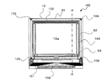
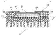
先ず、第1実施形態に係る電気光学装置について、図4及び図5を参照して説明する。ここに図4は、第1実施形態に係る電気光学装置の全体構成を示す斜視図であり、図5は、第1実施形態に係る電気光学装置の具体的な構成を示す断面図である。
次に、第2実施形態に係る電気光学装置について、図6を参照して説明する。ここに図6は、第2実施形態に係る電気光学装置の具体的な構成を示す断面図である。尚、第2実施形態は、上述の第1実施形態と比べて一部の構成が異なり、その他の構成については概ね同様である。このため第2実施形態では、第1実施形態と異なる部分について詳細に説明し、その他の重複する部分については適宜説明を省略する。
次に、第3実施形態に係る電気光学装置について、図7を参照して説明する。ここに図7は、第3実施形態に係る電気光学装置の具体的な構成を示す断面図である。尚、第3実施形態は、上述の第1実施形態と比べて一部の構成が異なり、その他の構成については概ね同様である。このため第3実施形態では、第1実施形態と異なる部分について詳細に説明し、その他の重複する部分については適宜説明を省略する。
次に、上述した電気光学装置である液晶装置を各種の電子機器に適用する場合について説明する。ここでは、本発明に係る電子機器として、投射型液晶プロジェクターを例にとる。図8は、本実施形態に係る投射型液晶プロジェクターの図式的断面図である。
Claims (4)
- 反射型の電気光学パネルと、
前記電気光学パネルの少なくとも側面に接着された第1保持部材と、
前記電気光学パネルの背面に接着され、放熱部を有する第2保持部材と
を備え、
前記第1保持部材は、前記第2保持部材より熱膨張係数の小さい材料を含み、前記第1保持部材と前記第2保持部材との間には、所定の間隙が設けられている
ことを特徴とする電気光学装置。 - 前記第1保持部材は、前記第2保持部材の側面に接合されていることを特徴とする請求項1に記載の電気光学装置。
- 前記所定の間隙には、熱伝導性を有する充填材が充填されていることを特徴とする請求項1または2に記載の電気光学装置。
- 請求項1から3のいずれか一項に記載の電気光学装置を具備してなることを特徴とする電子機器。
Priority Applications (4)
| Application Number | Priority Date | Filing Date | Title |
|---|---|---|---|
| JP2009107368A JP5487704B2 (ja) | 2009-04-27 | 2009-04-27 | 電気光学装置及び電子機器 |
| US12/753,980 US8988883B2 (en) | 2009-04-27 | 2010-04-05 | Electro-optic device and electronic device |
| KR1020100038376A KR20100118077A (ko) | 2009-04-27 | 2010-04-26 | 전기 광학 장치 및 전자 기기 |
| CN201010166754.6A CN101872079B (zh) | 2009-04-27 | 2010-04-27 | 电光装置及电子设备 |
Applications Claiming Priority (1)
| Application Number | Priority Date | Filing Date | Title |
|---|---|---|---|
| JP2009107368A JP5487704B2 (ja) | 2009-04-27 | 2009-04-27 | 電気光学装置及び電子機器 |
Publications (3)
| Publication Number | Publication Date |
|---|---|
| JP2010256653A JP2010256653A (ja) | 2010-11-11 |
| JP2010256653A5 JP2010256653A5 (ja) | 2012-05-31 |
| JP5487704B2 true JP5487704B2 (ja) | 2014-05-07 |
Family
ID=42991940
Family Applications (1)
| Application Number | Title | Priority Date | Filing Date |
|---|---|---|---|
| JP2009107368A Active JP5487704B2 (ja) | 2009-04-27 | 2009-04-27 | 電気光学装置及び電子機器 |
Country Status (4)
| Country | Link |
|---|---|
| US (1) | US8988883B2 (ja) |
| JP (1) | JP5487704B2 (ja) |
| KR (1) | KR20100118077A (ja) |
| CN (1) | CN101872079B (ja) |
Families Citing this family (15)
| Publication number | Priority date | Publication date | Assignee | Title |
|---|---|---|---|---|
| JP5598006B2 (ja) * | 2010-02-03 | 2014-10-01 | ソニー株式会社 | 液晶表示装置及び投射型表示装置 |
| JP5423547B2 (ja) * | 2010-04-05 | 2014-02-19 | セイコーエプソン株式会社 | 電気光学装置および電子機器 |
| JP2011221159A (ja) | 2010-04-07 | 2011-11-04 | Seiko Epson Corp | 放熱部材、電気光学装置および電子機器 |
| JP5445292B2 (ja) * | 2010-04-07 | 2014-03-19 | セイコーエプソン株式会社 | 放熱部材、電気光学装置および電子機器 |
| KR101209306B1 (ko) * | 2010-06-23 | 2012-12-06 | 엘지이노텍 주식회사 | 세라믹 기판 및 그의 제조 방법과 이미지 센서 패키지 및 그의 제조 방법 |
| KR101771559B1 (ko) * | 2011-01-05 | 2017-08-25 | 엘지전자 주식회사 | 디스플레이 장치 |
| JP5879707B2 (ja) * | 2011-03-16 | 2016-03-08 | ソニー株式会社 | 反射型液晶表示装置、及び投射型表示装置 |
| JP2013068873A (ja) * | 2011-09-26 | 2013-04-18 | Seiko Epson Corp | 電気光学モジュールおよび電子機器 |
| US20130113712A1 (en) * | 2011-11-04 | 2013-05-09 | Nokia Corporation | User Interface Panel Connection |
| TWI556040B (zh) * | 2012-07-11 | 2016-11-01 | 友達光電股份有限公司 | 背光模組以及顯示模組 |
| US20140284040A1 (en) * | 2013-03-22 | 2014-09-25 | International Business Machines Corporation | Heat spreading layer with high thermal conductivity |
| WO2014156434A1 (ja) * | 2013-03-29 | 2014-10-02 | シャープ株式会社 | アクティブマトリクス基板、及び表示装置 |
| TWI567457B (zh) * | 2014-04-07 | 2017-01-21 | 瑞儀光電股份有限公司 | 光學組件、背光模組及液晶顯示器 |
| KR101596348B1 (ko) * | 2014-12-29 | 2016-03-08 | 지에스알(주) | 텔레비젼의 방열장치 |
| JP6361939B2 (ja) * | 2016-03-08 | 2018-07-25 | パナソニックIpマネジメント株式会社 | 表示装置 |
Family Cites Families (74)
| Publication number | Priority date | Publication date | Assignee | Title |
|---|---|---|---|---|
| JPH03148199A (ja) * | 1989-11-02 | 1991-06-24 | Uchu Tsushin Kiso Gijutsu Kenkyusho:Kk | 実装ケースの伝熱構造 |
| JPH052164A (ja) * | 1991-01-28 | 1993-01-08 | Toshiba Corp | Lcdモジユール |
| US5146354A (en) * | 1991-05-07 | 1992-09-08 | Compaq Computer Corporation | LCD system with a backlight having a light source at a light pipe's edge and with the LCD enframed |
| JP3231820B2 (ja) * | 1991-12-17 | 2001-11-26 | ソニー株式会社 | 液晶表示装置 |
| JPH06194650A (ja) * | 1992-12-25 | 1994-07-15 | Citizen Watch Co Ltd | 表示装置 |
| EP0638832B1 (en) * | 1993-08-10 | 2000-03-22 | Canon Kabushiki Kaisha | Liquid crystal display apparatus |
| US5721602A (en) * | 1995-10-11 | 1998-02-24 | International Business Machines Corporation | Mechanical packaging and thermal management of flat mirror arrays |
| JPH09113906A (ja) * | 1995-10-13 | 1997-05-02 | Sony Corp | 透過型表示装置 |
| JPH10123964A (ja) * | 1996-08-30 | 1998-05-15 | Sony Corp | 液晶表示装置 |
| US5818564A (en) * | 1996-09-13 | 1998-10-06 | Raychem Corporation | Assembly including an active matrix liquid crystal display module |
| JPH10232629A (ja) * | 1997-02-20 | 1998-09-02 | Sony Corp | 液晶表示素子およびこれを用いた投射型液晶表示装置 |
| US6737790B2 (en) * | 1998-05-19 | 2004-05-18 | Canon Kabushiki Kaisha | Image forming apparatus having a heat insulating member |
| US6246459B1 (en) * | 1998-06-10 | 2001-06-12 | Tyco Electronics Corporation | Assembly including an active matrix liquid crystal display module and having plural environmental seals |
| JP2000089364A (ja) * | 1998-09-09 | 2000-03-31 | Seiko Epson Corp | 光変調装置およびこの光変調装置を利用した投写型表示装置 |
| US6731367B1 (en) * | 1998-12-04 | 2004-05-04 | Seiko Epson Corporation | Electro-optical panel, electro-optical panel module, and projection display device |
| JP3743190B2 (ja) * | 1999-02-02 | 2006-02-08 | セイコーエプソン株式会社 | 電気光学装置取り付けユニット及びそれを利用した投写型表示装置 |
| US6414781B1 (en) * | 1999-03-30 | 2002-07-02 | Seiko Epson Corporation | Electro-optical device and projection display device including the same |
| KR100603850B1 (ko) * | 2000-02-24 | 2006-07-24 | 엘지.필립스 엘시디 주식회사 | 액정표시장치용 배광장치의 도광판 및 시트 고정구조 |
| JP2002032031A (ja) * | 2000-05-12 | 2002-01-31 | Seiko Epson Corp | 電気光学装置の製造方法、端子の接続方法、電気光学装置および電子機器 |
| JP3888040B2 (ja) * | 2000-07-10 | 2007-02-28 | セイコーエプソン株式会社 | 光学部品およびこれを備えたプロジェクタ |
| JP4075303B2 (ja) * | 2000-11-01 | 2008-04-16 | セイコーエプソン株式会社 | プロジェクタ |
| EP1341028A4 (en) * | 2000-12-08 | 2006-05-10 | Sony Corp | Liquid crystal display and liquid crystal projector |
| JP2002189210A (ja) * | 2000-12-21 | 2002-07-05 | Sony Corp | 液晶表示装置 |
| TW567742B (en) * | 2001-03-22 | 2003-12-21 | Ind Tech Res Inst | Cooling apparatus of liquid crystal projector |
| JP2002296568A (ja) * | 2001-03-29 | 2002-10-09 | Victor Co Of Japan Ltd | 反射型液晶表示素子及びその製造方法 |
| JP3864862B2 (ja) * | 2002-04-04 | 2007-01-10 | セイコーエプソン株式会社 | 電気光学装置及び電子機器 |
| US6819464B2 (en) * | 2002-06-19 | 2004-11-16 | Seiko Epson Corporation | Optical modulator, optical device and projector |
| JP4181821B2 (ja) * | 2002-08-23 | 2008-11-19 | キヤノン株式会社 | 反射型液晶表示パネルの保持装置、反射型液晶表示パネルを用いた光学ユニット、投射型表示光学系および投射型画像表示装置 |
| JP2004133430A (ja) * | 2002-09-20 | 2004-04-30 | Sony Corp | 表示素子、表示装置、及びマイクロレンズアレイ |
| JP4137572B2 (ja) * | 2002-09-27 | 2008-08-20 | オリンパス株式会社 | 撮像装置 |
| JP2004118039A (ja) * | 2002-09-27 | 2004-04-15 | Seiko Epson Corp | 電気光学装置、及び電子機器 |
| US6815729B1 (en) * | 2002-10-09 | 2004-11-09 | Cypress Semiconductor Corp. | Electro-optical apparatus |
| JP3707470B2 (ja) * | 2002-12-20 | 2005-10-19 | セイコーエプソン株式会社 | 実装ケース入り電気光学装置及び投射型表示装置 |
| JP3722141B2 (ja) * | 2002-12-20 | 2005-11-30 | セイコーエプソン株式会社 | 実装ケース入り電気光学装置及び投射型表示装置並びに実装ケース |
| JP3736523B2 (ja) * | 2002-12-20 | 2006-01-18 | セイコーエプソン株式会社 | 実装ケース入り電気光学装置及び投射型表示装置並びに実装ケース |
| JP3736522B2 (ja) * | 2002-12-20 | 2006-01-18 | セイコーエプソン株式会社 | 実装ケース入り電気光学装置及び投射型表示装置並びに実装ケース |
| JP2004258621A (ja) * | 2003-02-06 | 2004-09-16 | Hitachi Displays Ltd | プロジェクタ用液晶表示装置 |
| TW566572U (en) * | 2003-03-07 | 2003-12-11 | Lite On Technology Corp | Flexible assembling device applied in an optical projection apparatus and its mechanism |
| JP3711987B2 (ja) * | 2003-03-27 | 2005-11-02 | セイコーエプソン株式会社 | 実装ケース入り電気光学装置及び投射型表示装置並びに実装ケース |
| JP3698147B2 (ja) * | 2003-04-22 | 2005-09-21 | セイコーエプソン株式会社 | 実装ケース入り電気光学装置及び投射型表示装置並びに実装ケース |
| JP3707480B2 (ja) * | 2003-04-22 | 2005-10-19 | セイコーエプソン株式会社 | 実装ケース入り電気光学装置及び投射型表示装置並びに実装ケース |
| GB2401250B (en) * | 2003-04-29 | 2006-05-17 | Agilent Technologies Inc | Heat sink |
| US7300182B2 (en) * | 2003-05-05 | 2007-11-27 | Lamina Lighting, Inc. | LED light sources for image projection systems |
| US6999318B2 (en) * | 2003-07-28 | 2006-02-14 | Honeywell International Inc. | Heatsinking electronic devices |
| JP4380295B2 (ja) * | 2003-10-29 | 2009-12-09 | ソニー株式会社 | 反射型液晶表示素子および画像投影装置 |
| JP4362410B2 (ja) * | 2004-04-22 | 2009-11-11 | Nec液晶テクノロジー株式会社 | バックライト装置及び液晶表示装置 |
| JP4296988B2 (ja) * | 2004-05-14 | 2009-07-15 | ソニー株式会社 | 液晶プロジェクター |
| TWM261006U (en) * | 2004-05-28 | 2005-04-01 | Au Optronics Corp | Heatsink sheet of optic-electric apparatus |
| US7365821B2 (en) * | 2004-07-02 | 2008-04-29 | Sony Corporation | Liquid crystal display having dummy bump connected to dummy lead for heat reduction |
| JP4421963B2 (ja) * | 2004-07-15 | 2010-02-24 | Necインフロンティア株式会社 | 電子機器 |
| JP5192811B2 (ja) * | 2004-09-10 | 2013-05-08 | ソウル セミコンダクター カンパニー リミテッド | 多重モールド樹脂を有する発光ダイオードパッケージ |
| TWI255377B (en) * | 2004-11-05 | 2006-05-21 | Au Optronics Corp | Backlight module |
| KR100580753B1 (ko) * | 2004-12-17 | 2006-05-15 | 엘지이노텍 주식회사 | 발광소자 패키지 |
| US7710531B2 (en) * | 2005-02-15 | 2010-05-04 | Denso Corporation | Liquid crystal display apparatus |
| JP4238867B2 (ja) * | 2005-03-01 | 2009-03-18 | セイコーエプソン株式会社 | 冷却ユニットの製造方法、冷却ユニット、光学装置、並びにプロジェクタ |
| JP2006258883A (ja) * | 2005-03-15 | 2006-09-28 | Seiko Epson Corp | 電気光学装置、電気光学装置の製造方法 |
| KR20060104081A (ko) * | 2005-03-29 | 2006-10-09 | 삼성전자주식회사 | 액정표시장치 |
| KR20060107150A (ko) * | 2005-04-07 | 2006-10-13 | 삼성에스디아이 주식회사 | 냉각수단을 구비한 영상표시장치 |
| JP2007121505A (ja) * | 2005-10-26 | 2007-05-17 | Victor Co Of Japan Ltd | 反射型液晶表示装置 |
| KR20070047668A (ko) * | 2005-11-02 | 2007-05-07 | 삼성에스디아이 주식회사 | 온도차 감소를 위한 평면표시장치 |
| JP2007199153A (ja) | 2006-01-24 | 2007-08-09 | Victor Co Of Japan Ltd | 反射型液晶表示装置 |
| JP4572342B2 (ja) * | 2006-02-21 | 2010-11-04 | セイコーエプソン株式会社 | 電子機器 |
| JP4432937B2 (ja) * | 2006-06-06 | 2010-03-17 | セイコーエプソン株式会社 | 電気光学装置、及びこれを備えた電子機器 |
| KR20080007961A (ko) * | 2006-07-19 | 2008-01-23 | 알티전자 주식회사 | 엘이디 모듈의 냉각 장치 및 그 제조 방법 |
| JP2008060204A (ja) * | 2006-08-30 | 2008-03-13 | Nec Lcd Technologies Ltd | Ledバックライトユニットおよびそれを用いた液晶表示装置 |
| JP4901396B2 (ja) * | 2006-09-28 | 2012-03-21 | シチズンファインテックミヨタ株式会社 | 液晶表示装置 |
| DE102006048230B4 (de) * | 2006-10-11 | 2012-11-08 | Osram Ag | Leuchtdiodensystem, Verfahren zur Herstellung eines solchen und Hinterleuchtungseinrichtung |
| TWI323384B (en) * | 2007-04-09 | 2010-04-11 | Coretronic Corp | Light valve device |
| KR100877413B1 (ko) * | 2007-06-04 | 2009-01-07 | 엘지전자 주식회사 | 백라이트 유닛 및 이를 구비하는 액정 표시장치 |
| US7934862B2 (en) * | 2007-09-24 | 2011-05-03 | Munisamy Anandan | UV based color pixel backlight for liquid crystal display |
| TWI345127B (en) * | 2007-11-27 | 2011-07-11 | Coretronic Corp | Dmd module |
| US20090213548A1 (en) * | 2008-02-21 | 2009-08-27 | Kempers Roger S | Thermally conductive periodically structured gap fillers and method for utilizing same |
| JP5386941B2 (ja) * | 2008-11-14 | 2014-01-15 | セイコーエプソン株式会社 | 電気光学装置及びその製造方法並びに電子機器 |
| CN101996535A (zh) * | 2009-08-25 | 2011-03-30 | 精工爱普生株式会社 | 电光学装置和电子设备 |
-
2009
- 2009-04-27 JP JP2009107368A patent/JP5487704B2/ja active Active
-
2010
- 2010-04-05 US US12/753,980 patent/US8988883B2/en active Active
- 2010-04-26 KR KR1020100038376A patent/KR20100118077A/ko not_active Application Discontinuation
- 2010-04-27 CN CN201010166754.6A patent/CN101872079B/zh active Active
Also Published As
| Publication number | Publication date |
|---|---|
| CN101872079B (zh) | 2015-10-14 |
| US20100271782A1 (en) | 2010-10-28 |
| CN101872079A (zh) | 2010-10-27 |
| KR20100118077A (ko) | 2010-11-04 |
| JP2010256653A (ja) | 2010-11-11 |
| US8988883B2 (en) | 2015-03-24 |
Similar Documents
| Publication | Publication Date | Title |
|---|---|---|
| JP5487704B2 (ja) | 電気光学装置及び電子機器 | |
| JP5504683B2 (ja) | 電気光学装置及び電子機器 | |
| JP5533001B2 (ja) | 電気光学装置及び電子機器 | |
| JP5515813B2 (ja) | 電気光学装置及び電子機器 | |
| JP5731122B2 (ja) | 電気光学装置及び電子機器 | |
| JP5672718B2 (ja) | 電気光学装置及び電子機器 | |
| JP2010256666A (ja) | 電気光学装置及び電子機器 | |
| JP5544749B2 (ja) | 電気光学装置及び電子機器 | |
| JP5381282B2 (ja) | 電気光学装置及び電子機器 | |
| JP2015197650A (ja) | 電気光学装置、及び電子機器 | |
| JP2010256662A (ja) | 電気光学装置及び電子機器 | |
| JP6108004B2 (ja) | 電気光学装置及び電子機器 | |
| JP5187268B2 (ja) | 電気光学装置及び電子機器 | |
| JP5928571B2 (ja) | 電気光学装置及び電子機器 | |
| JP2015200687A (ja) | 電気光学装置、及び電子機器 | |
| JP2010256667A (ja) | 電気光学装置及び電子機器 | |
| JP2010256663A (ja) | 電気光学装置及び電子機器 | |
| JP5181736B2 (ja) | 電気光学装置及び電子機器 | |
| JP2015200688A (ja) | 電気光学装置、及び電子機器 | |
| JP2010175818A (ja) | 電気光学装置及び電子機器 |
Legal Events
| Date | Code | Title | Description |
|---|---|---|---|
| RD01 | Notification of change of attorney |
Free format text: JAPANESE INTERMEDIATE CODE: A7421 Effective date: 20120327 |
|
| A521 | Written amendment |
Free format text: JAPANESE INTERMEDIATE CODE: A523 Effective date: 20120406 |
|
| A621 | Written request for application examination |
Free format text: JAPANESE INTERMEDIATE CODE: A621 Effective date: 20120406 |
|
| A977 | Report on retrieval |
Free format text: JAPANESE INTERMEDIATE CODE: A971007 Effective date: 20130307 |
|
| A131 | Notification of reasons for refusal |
Free format text: JAPANESE INTERMEDIATE CODE: A131 Effective date: 20130319 |
|
| A521 | Written amendment |
Free format text: JAPANESE INTERMEDIATE CODE: A523 Effective date: 20130517 |
|
| TRDD | Decision of grant or rejection written | ||
| A01 | Written decision to grant a patent or to grant a registration (utility model) |
Free format text: JAPANESE INTERMEDIATE CODE: A01 Effective date: 20140128 |
|
| A61 | First payment of annual fees (during grant procedure) |
Free format text: JAPANESE INTERMEDIATE CODE: A61 Effective date: 20140210 |
|
| R150 | Certificate of patent or registration of utility model |
Ref document number: 5487704 Country of ref document: JP Free format text: JAPANESE INTERMEDIATE CODE: R150 |
|
| S531 | Written request for registration of change of domicile |
Free format text: JAPANESE INTERMEDIATE CODE: R313531 |
|
| R350 | Written notification of registration of transfer |
Free format text: JAPANESE INTERMEDIATE CODE: R350 |