EP1398778A2 - Optischer Datenaufzeichnungsträger und Verfahren für optische Aufzeichnung - Google Patents
Optischer Datenaufzeichnungsträger und Verfahren für optische Aufzeichnung Download PDFInfo
- Publication number
- EP1398778A2 EP1398778A2 EP03025307A EP03025307A EP1398778A2 EP 1398778 A2 EP1398778 A2 EP 1398778A2 EP 03025307 A EP03025307 A EP 03025307A EP 03025307 A EP03025307 A EP 03025307A EP 1398778 A2 EP1398778 A2 EP 1398778A2
- Authority
- EP
- European Patent Office
- Prior art keywords
- layer
- recording
- thickness
- crystallization
- composition
- Prior art date
- Legal status (The legal status is an assumption and is not a legal conclusion. Google has not performed a legal analysis and makes no representation as to the accuracy of the status listed.)
- Granted
Links
- 230000003287 optical effect Effects 0.000 title claims abstract description 118
- 238000000034 method Methods 0.000 title claims description 31
- 239000010410 layer Substances 0.000 claims abstract description 348
- 239000000203 mixture Substances 0.000 claims abstract description 108
- 239000011241 protective layer Substances 0.000 claims abstract description 55
- 239000000758 substrate Substances 0.000 claims abstract description 36
- 238000002425 crystallisation Methods 0.000 claims description 118
- 230000008025 crystallization Effects 0.000 claims description 118
- 150000001875 compounds Chemical class 0.000 claims description 21
- 230000008018 melting Effects 0.000 claims description 19
- 238000002844 melting Methods 0.000 claims description 19
- 229910052709 silver Inorganic materials 0.000 claims description 16
- 229910052751 metal Inorganic materials 0.000 claims description 15
- 239000002184 metal Substances 0.000 claims description 15
- 229910052725 zinc Inorganic materials 0.000 claims description 15
- 229910052782 aluminium Inorganic materials 0.000 claims description 13
- 150000001786 chalcogen compounds Chemical class 0.000 claims description 11
- 230000001678 irradiating effect Effects 0.000 claims description 11
- 229910052737 gold Inorganic materials 0.000 claims description 10
- 238000000354 decomposition reaction Methods 0.000 claims description 5
- 238000012935 Averaging Methods 0.000 claims description 2
- 230000008021 deposition Effects 0.000 claims 1
- VYPSYNLAJGMNEJ-UHFFFAOYSA-N Silicium dioxide Chemical compound O=[Si]=O VYPSYNLAJGMNEJ-UHFFFAOYSA-N 0.000 description 94
- 239000000377 silicon dioxide Substances 0.000 description 47
- 229910052681 coesite Inorganic materials 0.000 description 46
- 229910052906 cristobalite Inorganic materials 0.000 description 46
- 229910052682 stishovite Inorganic materials 0.000 description 46
- 229910052905 tridymite Inorganic materials 0.000 description 46
- 239000000956 alloy Substances 0.000 description 42
- 229910045601 alloy Inorganic materials 0.000 description 41
- 230000000694 effects Effects 0.000 description 34
- 230000005496 eutectics Effects 0.000 description 33
- 238000011156 evaluation Methods 0.000 description 30
- 239000000463 material Substances 0.000 description 30
- 229920005989 resin Polymers 0.000 description 25
- 239000011347 resin Substances 0.000 description 25
- 238000001755 magnetron sputter deposition Methods 0.000 description 23
- 239000004417 polycarbonate Substances 0.000 description 23
- 229920000515 polycarbonate Polymers 0.000 description 23
- 230000003252 repetitive effect Effects 0.000 description 21
- 238000001953 recrystallisation Methods 0.000 description 20
- 230000006866 deterioration Effects 0.000 description 18
- 238000001816 cooling Methods 0.000 description 17
- 239000013078 crystal Substances 0.000 description 16
- 239000012071 phase Substances 0.000 description 16
- 238000002310 reflectometry Methods 0.000 description 16
- 229910018321 SbTe Inorganic materials 0.000 description 14
- 238000005191 phase separation Methods 0.000 description 12
- 229910017629 Sb2Te3 Inorganic materials 0.000 description 11
- 230000015572 biosynthetic process Effects 0.000 description 11
- 229910052710 silicon Inorganic materials 0.000 description 11
- 239000000654 additive Substances 0.000 description 10
- 229910052732 germanium Inorganic materials 0.000 description 10
- 230000001771 impaired effect Effects 0.000 description 10
- 239000012535 impurity Substances 0.000 description 10
- 229910002058 ternary alloy Inorganic materials 0.000 description 10
- 230000000996 additive effect Effects 0.000 description 9
- 229910002056 binary alloy Inorganic materials 0.000 description 9
- 238000004544 sputter deposition Methods 0.000 description 9
- 230000008859 change Effects 0.000 description 8
- 230000000052 comparative effect Effects 0.000 description 8
- 229910052738 indium Inorganic materials 0.000 description 8
- 238000005204 segregation Methods 0.000 description 8
- IJGRMHOSHXDMSA-UHFFFAOYSA-N Atomic nitrogen Chemical compound N#N IJGRMHOSHXDMSA-UHFFFAOYSA-N 0.000 description 6
- 238000005336 cracking Methods 0.000 description 6
- 230000017525 heat dissipation Effects 0.000 description 6
- 238000010438 heat treatment Methods 0.000 description 6
- 229910052749 magnesium Inorganic materials 0.000 description 6
- 150000004767 nitrides Chemical class 0.000 description 6
- 239000002245 particle Substances 0.000 description 6
- 229910052718 tin Inorganic materials 0.000 description 6
- 229910052719 titanium Inorganic materials 0.000 description 6
- 229910052726 zirconium Inorganic materials 0.000 description 6
- 230000007797 corrosion Effects 0.000 description 5
- 238000005260 corrosion Methods 0.000 description 5
- 229910001325 element alloy Inorganic materials 0.000 description 5
- 239000006023 eutectic alloy Substances 0.000 description 5
- 230000006872 improvement Effects 0.000 description 5
- 229910052745 lead Inorganic materials 0.000 description 5
- 239000011159 matrix material Substances 0.000 description 5
- 229910052758 niobium Inorganic materials 0.000 description 5
- 239000004033 plastic Substances 0.000 description 5
- 229910052715 tantalum Inorganic materials 0.000 description 5
- 229910052720 vanadium Inorganic materials 0.000 description 5
- 229910000838 Al alloy Inorganic materials 0.000 description 4
- 229910000618 GeSbTe Inorganic materials 0.000 description 4
- UCKMPCXJQFINFW-UHFFFAOYSA-N Sulphide Chemical compound [S-2] UCKMPCXJQFINFW-UHFFFAOYSA-N 0.000 description 4
- QVGXLLKOCUKJST-UHFFFAOYSA-N atomic oxygen Chemical compound [O] QVGXLLKOCUKJST-UHFFFAOYSA-N 0.000 description 4
- 229910052804 chromium Inorganic materials 0.000 description 4
- 239000007789 gas Substances 0.000 description 4
- 229910052760 oxygen Inorganic materials 0.000 description 4
- 239000001301 oxygen Substances 0.000 description 4
- KRHYYFGTRYWZRS-UHFFFAOYSA-M Fluoride anion Chemical compound [F-] KRHYYFGTRYWZRS-UHFFFAOYSA-M 0.000 description 3
- 229910005900 GeTe Inorganic materials 0.000 description 3
- 229910000979 O alloy Inorganic materials 0.000 description 3
- 229910007657 ZnSb Inorganic materials 0.000 description 3
- 229910052787 antimony Inorganic materials 0.000 description 3
- 230000005540 biological transmission Effects 0.000 description 3
- 229910052791 calcium Inorganic materials 0.000 description 3
- 229910052798 chalcogen Inorganic materials 0.000 description 3
- 150000001787 chalcogens Chemical class 0.000 description 3
- 239000010408 film Substances 0.000 description 3
- 230000006870 function Effects 0.000 description 3
- 229910000765 intermetallic Inorganic materials 0.000 description 3
- 229910052757 nitrogen Inorganic materials 0.000 description 3
- 239000002244 precipitate Substances 0.000 description 3
- 230000008569 process Effects 0.000 description 3
- 229940065287 selenium compound Drugs 0.000 description 3
- 150000003343 selenium compounds Chemical class 0.000 description 3
- 230000035945 sensitivity Effects 0.000 description 3
- 239000007790 solid phase Substances 0.000 description 3
- 239000010409 thin film Substances 0.000 description 3
- QVQLCTNNEUAWMS-UHFFFAOYSA-N barium oxide Chemical compound [Ba]=O QVQLCTNNEUAWMS-UHFFFAOYSA-N 0.000 description 2
- 229910052796 boron Inorganic materials 0.000 description 2
- 239000002131 composite material Substances 0.000 description 2
- 230000007423 decrease Effects 0.000 description 2
- 230000007812 deficiency Effects 0.000 description 2
- 239000011521 glass Substances 0.000 description 2
- 229910052735 hafnium Inorganic materials 0.000 description 2
- WPYVAWXEWQSOGY-UHFFFAOYSA-N indium antimonide Chemical compound [Sb]#[In] WPYVAWXEWQSOGY-UHFFFAOYSA-N 0.000 description 2
- 229910052746 lanthanum Inorganic materials 0.000 description 2
- 229910052748 manganese Inorganic materials 0.000 description 2
- 238000005259 measurement Methods 0.000 description 2
- 230000007246 mechanism Effects 0.000 description 2
- 239000000155 melt Substances 0.000 description 2
- 229910052750 molybdenum Inorganic materials 0.000 description 2
- 229910052763 palladium Inorganic materials 0.000 description 2
- 229910052697 platinum Inorganic materials 0.000 description 2
- 238000001556 precipitation Methods 0.000 description 2
- 238000002360 preparation method Methods 0.000 description 2
- 239000011253 protective coating Substances 0.000 description 2
- 229910052761 rare earth metal Inorganic materials 0.000 description 2
- -1 rare earth sulfide Chemical class 0.000 description 2
- 229910052711 selenium Inorganic materials 0.000 description 2
- 239000011669 selenium Substances 0.000 description 2
- 230000000087 stabilizing effect Effects 0.000 description 2
- 238000003860 storage Methods 0.000 description 2
- 239000000126 substance Substances 0.000 description 2
- 150000004763 sulfides Chemical class 0.000 description 2
- 229910052717 sulfur Inorganic materials 0.000 description 2
- 229910052721 tungsten Inorganic materials 0.000 description 2
- 229910001316 Ag alloy Inorganic materials 0.000 description 1
- 229910021365 Al-Mg-Si alloy Inorganic materials 0.000 description 1
- 229910017083 AlN Inorganic materials 0.000 description 1
- 229910052684 Cerium Inorganic materials 0.000 description 1
- 229910052691 Erbium Inorganic materials 0.000 description 1
- 229910052689 Holmium Inorganic materials 0.000 description 1
- 229910017586 La2S3 Inorganic materials 0.000 description 1
- 229910002319 LaF3 Inorganic materials 0.000 description 1
- 229910017557 NdF3 Inorganic materials 0.000 description 1
- 229910052779 Neodymium Inorganic materials 0.000 description 1
- 229910052581 Si3N4 Inorganic materials 0.000 description 1
- 229910004299 TbF3 Inorganic materials 0.000 description 1
- 229910052771 Terbium Inorganic materials 0.000 description 1
- 238000002441 X-ray diffraction Methods 0.000 description 1
- 229910052769 Ytterbium Inorganic materials 0.000 description 1
- 238000010521 absorption reaction Methods 0.000 description 1
- 229910000905 alloy phase Inorganic materials 0.000 description 1
- 238000005280 amorphization Methods 0.000 description 1
- 238000004458 analytical method Methods 0.000 description 1
- 238000000137 annealing Methods 0.000 description 1
- 229910052799 carbon Inorganic materials 0.000 description 1
- 238000006243 chemical reaction Methods 0.000 description 1
- 238000010276 construction Methods 0.000 description 1
- 238000011109 contamination Methods 0.000 description 1
- 229910052802 copper Inorganic materials 0.000 description 1
- 230000007547 defect Effects 0.000 description 1
- 230000002950 deficient Effects 0.000 description 1
- 238000013461 design Methods 0.000 description 1
- 230000002542 deteriorative effect Effects 0.000 description 1
- 238000009792 diffusion process Methods 0.000 description 1
- 238000001803 electron scattering Methods 0.000 description 1
- 150000002222 fluorine compounds Chemical class 0.000 description 1
- 238000011423 initialization method Methods 0.000 description 1
- 229910052747 lanthanoid Inorganic materials 0.000 description 1
- 150000002602 lanthanoids Chemical class 0.000 description 1
- 229910052744 lithium Inorganic materials 0.000 description 1
- 230000005415 magnetization Effects 0.000 description 1
- 238000004519 manufacturing process Methods 0.000 description 1
- 150000001247 metal acetylides Chemical class 0.000 description 1
- 229910003465 moissanite Inorganic materials 0.000 description 1
- 230000003647 oxidation Effects 0.000 description 1
- 238000007254 oxidation reaction Methods 0.000 description 1
- SIWVEOZUMHYXCS-UHFFFAOYSA-N oxo(oxoyttriooxy)yttrium Chemical compound O=[Y]O[Y]=O SIWVEOZUMHYXCS-UHFFFAOYSA-N 0.000 description 1
- BPUBBGLMJRNUCC-UHFFFAOYSA-N oxygen(2-);tantalum(5+) Chemical compound [O-2].[O-2].[O-2].[O-2].[O-2].[Ta+5].[Ta+5] BPUBBGLMJRNUCC-UHFFFAOYSA-N 0.000 description 1
- 229920005668 polycarbonate resin Polymers 0.000 description 1
- 239000004431 polycarbonate resin Substances 0.000 description 1
- 229920000642 polymer Polymers 0.000 description 1
- 239000000047 product Substances 0.000 description 1
- 238000010791 quenching Methods 0.000 description 1
- 230000000171 quenching effect Effects 0.000 description 1
- 150000002910 rare earth metals Chemical class 0.000 description 1
- 230000009467 reduction Effects 0.000 description 1
- 230000002441 reversible effect Effects 0.000 description 1
- 229910052703 rhodium Inorganic materials 0.000 description 1
- 239000000523 sample Substances 0.000 description 1
- 229910052706 scandium Inorganic materials 0.000 description 1
- 238000006748 scratching Methods 0.000 description 1
- 230000002393 scratching effect Effects 0.000 description 1
- 239000004065 semiconductor Substances 0.000 description 1
- 238000004904 shortening Methods 0.000 description 1
- 229910010271 silicon carbide Inorganic materials 0.000 description 1
- 235000012239 silicon dioxide Nutrition 0.000 description 1
- 239000007787 solid Substances 0.000 description 1
- 238000004528 spin coating Methods 0.000 description 1
- 229910052712 strontium Inorganic materials 0.000 description 1
- 229910001936 tantalum oxide Inorganic materials 0.000 description 1
- 229920001187 thermosetting polymer Polymers 0.000 description 1
- BYMUNNMMXKDFEZ-UHFFFAOYSA-K trifluorolanthanum Chemical compound F[La](F)F BYMUNNMMXKDFEZ-UHFFFAOYSA-K 0.000 description 1
- LKNRQYTYDPPUOX-UHFFFAOYSA-K trifluoroterbium Chemical compound F[Tb](F)F LKNRQYTYDPPUOX-UHFFFAOYSA-K 0.000 description 1
- 238000001771 vacuum deposition Methods 0.000 description 1
- 238000007740 vapor deposition Methods 0.000 description 1
- 238000004876 x-ray fluorescence Methods 0.000 description 1
- 229910052727 yttrium Inorganic materials 0.000 description 1
Images

Classifications
-
- G—PHYSICS
- G11—INFORMATION STORAGE
- G11B—INFORMATION STORAGE BASED ON RELATIVE MOVEMENT BETWEEN RECORD CARRIER AND TRANSDUCER
- G11B7/00—Recording or reproducing by optical means, e.g. recording using a thermal beam of optical radiation by modifying optical properties or the physical structure, reproducing using an optical beam at lower power by sensing optical properties; Record carriers therefor
- G11B7/24—Record carriers characterised by shape, structure or physical properties, or by the selection of the material
- G11B7/241—Record carriers characterised by shape, structure or physical properties, or by the selection of the material characterised by the selection of the material
- G11B7/242—Record carriers characterised by shape, structure or physical properties, or by the selection of the material characterised by the selection of the material of recording layers
- G11B7/243—Record carriers characterised by shape, structure or physical properties, or by the selection of the material characterised by the selection of the material of recording layers comprising inorganic materials only, e.g. ablative layers
-
- G—PHYSICS
- G11—INFORMATION STORAGE
- G11B—INFORMATION STORAGE BASED ON RELATIVE MOVEMENT BETWEEN RECORD CARRIER AND TRANSDUCER
- G11B7/00—Recording or reproducing by optical means, e.g. recording using a thermal beam of optical radiation by modifying optical properties or the physical structure, reproducing using an optical beam at lower power by sensing optical properties; Record carriers therefor
- G11B7/004—Recording, reproducing or erasing methods; Read, write or erase circuits therefor
- G11B7/0045—Recording
-
- G—PHYSICS
- G11—INFORMATION STORAGE
- G11B—INFORMATION STORAGE BASED ON RELATIVE MOVEMENT BETWEEN RECORD CARRIER AND TRANSDUCER
- G11B7/00—Recording or reproducing by optical means, e.g. recording using a thermal beam of optical radiation by modifying optical properties or the physical structure, reproducing using an optical beam at lower power by sensing optical properties; Record carriers therefor
- G11B7/004—Recording, reproducing or erasing methods; Read, write or erase circuits therefor
- G11B7/006—Overwriting
- G11B7/0062—Overwriting strategies, e.g. recording pulse sequences with erasing level used for phase-change media
-
- G—PHYSICS
- G11—INFORMATION STORAGE
- G11B—INFORMATION STORAGE BASED ON RELATIVE MOVEMENT BETWEEN RECORD CARRIER AND TRANSDUCER
- G11B7/00—Recording or reproducing by optical means, e.g. recording using a thermal beam of optical radiation by modifying optical properties or the physical structure, reproducing using an optical beam at lower power by sensing optical properties; Record carriers therefor
- G11B7/12—Heads, e.g. forming of the optical beam spot or modulation of the optical beam
- G11B7/125—Optical beam sources therefor, e.g. laser control circuitry specially adapted for optical storage devices; Modulators, e.g. means for controlling the size or intensity of optical spots or optical traces
- G11B7/126—Circuits, methods or arrangements for laser control or stabilisation
-
- G—PHYSICS
- G11—INFORMATION STORAGE
- G11B—INFORMATION STORAGE BASED ON RELATIVE MOVEMENT BETWEEN RECORD CARRIER AND TRANSDUCER
- G11B7/00—Recording or reproducing by optical means, e.g. recording using a thermal beam of optical radiation by modifying optical properties or the physical structure, reproducing using an optical beam at lower power by sensing optical properties; Record carriers therefor
- G11B7/24—Record carriers characterised by shape, structure or physical properties, or by the selection of the material
- G11B7/2403—Layers; Shape, structure or physical properties thereof
- G11B7/24067—Combinations of two or more layers with specific interrelation
-
- G—PHYSICS
- G11—INFORMATION STORAGE
- G11B—INFORMATION STORAGE BASED ON RELATIVE MOVEMENT BETWEEN RECORD CARRIER AND TRANSDUCER
- G11B7/00—Recording or reproducing by optical means, e.g. recording using a thermal beam of optical radiation by modifying optical properties or the physical structure, reproducing using an optical beam at lower power by sensing optical properties; Record carriers therefor
- G11B7/24—Record carriers characterised by shape, structure or physical properties, or by the selection of the material
- G11B7/241—Record carriers characterised by shape, structure or physical properties, or by the selection of the material characterised by the selection of the material
- G11B7/242—Record carriers characterised by shape, structure or physical properties, or by the selection of the material characterised by the selection of the material of recording layers
- G11B7/243—Record carriers characterised by shape, structure or physical properties, or by the selection of the material characterised by the selection of the material of recording layers comprising inorganic materials only, e.g. ablative layers
- G11B7/2433—Metals or elements of Groups 13, 14, 15 or 16 of the Periodic Table, e.g. B, Si, Ge, As, Sb, Bi, Se or Te
-
- G—PHYSICS
- G11—INFORMATION STORAGE
- G11B—INFORMATION STORAGE BASED ON RELATIVE MOVEMENT BETWEEN RECORD CARRIER AND TRANSDUCER
- G11B7/00—Recording or reproducing by optical means, e.g. recording using a thermal beam of optical radiation by modifying optical properties or the physical structure, reproducing using an optical beam at lower power by sensing optical properties; Record carriers therefor
- G11B7/24—Record carriers characterised by shape, structure or physical properties, or by the selection of the material
- G11B7/241—Record carriers characterised by shape, structure or physical properties, or by the selection of the material characterised by the selection of the material
- G11B7/252—Record carriers characterised by shape, structure or physical properties, or by the selection of the material characterised by the selection of the material of layers other than recording layers
- G11B7/254—Record carriers characterised by shape, structure or physical properties, or by the selection of the material characterised by the selection of the material of layers other than recording layers of protective topcoat layers
- G11B7/2542—Record carriers characterised by shape, structure or physical properties, or by the selection of the material characterised by the selection of the material of layers other than recording layers of protective topcoat layers consisting essentially of organic resins
-
- G—PHYSICS
- G11—INFORMATION STORAGE
- G11B—INFORMATION STORAGE BASED ON RELATIVE MOVEMENT BETWEEN RECORD CARRIER AND TRANSDUCER
- G11B7/00—Recording or reproducing by optical means, e.g. recording using a thermal beam of optical radiation by modifying optical properties or the physical structure, reproducing using an optical beam at lower power by sensing optical properties; Record carriers therefor
- G11B7/24—Record carriers characterised by shape, structure or physical properties, or by the selection of the material
- G11B7/241—Record carriers characterised by shape, structure or physical properties, or by the selection of the material characterised by the selection of the material
- G11B7/252—Record carriers characterised by shape, structure or physical properties, or by the selection of the material characterised by the selection of the material of layers other than recording layers
- G11B7/257—Record carriers characterised by shape, structure or physical properties, or by the selection of the material characterised by the selection of the material of layers other than recording layers of layers having properties involved in recording or reproduction, e.g. optical interference layers or sensitising layers or dielectric layers, which are protecting the recording layers
-
- G—PHYSICS
- G11—INFORMATION STORAGE
- G11B—INFORMATION STORAGE BASED ON RELATIVE MOVEMENT BETWEEN RECORD CARRIER AND TRANSDUCER
- G11B7/00—Recording or reproducing by optical means, e.g. recording using a thermal beam of optical radiation by modifying optical properties or the physical structure, reproducing using an optical beam at lower power by sensing optical properties; Record carriers therefor
- G11B7/24—Record carriers characterised by shape, structure or physical properties, or by the selection of the material
- G11B7/241—Record carriers characterised by shape, structure or physical properties, or by the selection of the material characterised by the selection of the material
- G11B7/252—Record carriers characterised by shape, structure or physical properties, or by the selection of the material characterised by the selection of the material of layers other than recording layers
- G11B7/258—Record carriers characterised by shape, structure or physical properties, or by the selection of the material characterised by the selection of the material of layers other than recording layers of reflective layers
-
- G—PHYSICS
- G11—INFORMATION STORAGE
- G11B—INFORMATION STORAGE BASED ON RELATIVE MOVEMENT BETWEEN RECORD CARRIER AND TRANSDUCER
- G11B7/00—Recording or reproducing by optical means, e.g. recording using a thermal beam of optical radiation by modifying optical properties or the physical structure, reproducing using an optical beam at lower power by sensing optical properties; Record carriers therefor
- G11B7/24—Record carriers characterised by shape, structure or physical properties, or by the selection of the material
- G11B7/26—Apparatus or processes specially adapted for the manufacture of record carriers
- G11B7/268—Post-production operations, e.g. initialising phase-change recording layers, checking for defects
-
- G—PHYSICS
- G11—INFORMATION STORAGE
- G11B—INFORMATION STORAGE BASED ON RELATIVE MOVEMENT BETWEEN RECORD CARRIER AND TRANSDUCER
- G11B7/00—Recording or reproducing by optical means, e.g. recording using a thermal beam of optical radiation by modifying optical properties or the physical structure, reproducing using an optical beam at lower power by sensing optical properties; Record carriers therefor
- G11B7/24—Record carriers characterised by shape, structure or physical properties, or by the selection of the material
- G11B7/241—Record carriers characterised by shape, structure or physical properties, or by the selection of the material characterised by the selection of the material
- G11B7/242—Record carriers characterised by shape, structure or physical properties, or by the selection of the material characterised by the selection of the material of recording layers
- G11B7/243—Record carriers characterised by shape, structure or physical properties, or by the selection of the material characterised by the selection of the material of recording layers comprising inorganic materials only, e.g. ablative layers
- G11B2007/24302—Metals or metalloids
- G11B2007/24304—Metals or metalloids group 2 or 12 elements (e.g. Be, Ca, Mg, Zn, Cd)
-
- G—PHYSICS
- G11—INFORMATION STORAGE
- G11B—INFORMATION STORAGE BASED ON RELATIVE MOVEMENT BETWEEN RECORD CARRIER AND TRANSDUCER
- G11B7/00—Recording or reproducing by optical means, e.g. recording using a thermal beam of optical radiation by modifying optical properties or the physical structure, reproducing using an optical beam at lower power by sensing optical properties; Record carriers therefor
- G11B7/24—Record carriers characterised by shape, structure or physical properties, or by the selection of the material
- G11B7/241—Record carriers characterised by shape, structure or physical properties, or by the selection of the material characterised by the selection of the material
- G11B7/242—Record carriers characterised by shape, structure or physical properties, or by the selection of the material characterised by the selection of the material of recording layers
- G11B7/243—Record carriers characterised by shape, structure or physical properties, or by the selection of the material characterised by the selection of the material of recording layers comprising inorganic materials only, e.g. ablative layers
- G11B2007/24302—Metals or metalloids
- G11B2007/2431—Metals or metalloids group 13 elements (B, Al, Ga, In)
-
- G—PHYSICS
- G11—INFORMATION STORAGE
- G11B—INFORMATION STORAGE BASED ON RELATIVE MOVEMENT BETWEEN RECORD CARRIER AND TRANSDUCER
- G11B7/00—Recording or reproducing by optical means, e.g. recording using a thermal beam of optical radiation by modifying optical properties or the physical structure, reproducing using an optical beam at lower power by sensing optical properties; Record carriers therefor
- G11B7/24—Record carriers characterised by shape, structure or physical properties, or by the selection of the material
- G11B7/241—Record carriers characterised by shape, structure or physical properties, or by the selection of the material characterised by the selection of the material
- G11B7/242—Record carriers characterised by shape, structure or physical properties, or by the selection of the material characterised by the selection of the material of recording layers
- G11B7/243—Record carriers characterised by shape, structure or physical properties, or by the selection of the material characterised by the selection of the material of recording layers comprising inorganic materials only, e.g. ablative layers
- G11B2007/24302—Metals or metalloids
- G11B2007/24312—Metals or metalloids group 14 elements (e.g. Si, Ge, Sn)
-
- G—PHYSICS
- G11—INFORMATION STORAGE
- G11B—INFORMATION STORAGE BASED ON RELATIVE MOVEMENT BETWEEN RECORD CARRIER AND TRANSDUCER
- G11B7/00—Recording or reproducing by optical means, e.g. recording using a thermal beam of optical radiation by modifying optical properties or the physical structure, reproducing using an optical beam at lower power by sensing optical properties; Record carriers therefor
- G11B7/24—Record carriers characterised by shape, structure or physical properties, or by the selection of the material
- G11B7/241—Record carriers characterised by shape, structure or physical properties, or by the selection of the material characterised by the selection of the material
- G11B7/242—Record carriers characterised by shape, structure or physical properties, or by the selection of the material characterised by the selection of the material of recording layers
- G11B7/243—Record carriers characterised by shape, structure or physical properties, or by the selection of the material characterised by the selection of the material of recording layers comprising inorganic materials only, e.g. ablative layers
- G11B2007/24302—Metals or metalloids
- G11B2007/24314—Metals or metalloids group 15 elements (e.g. Sb, Bi)
-
- G—PHYSICS
- G11—INFORMATION STORAGE
- G11B—INFORMATION STORAGE BASED ON RELATIVE MOVEMENT BETWEEN RECORD CARRIER AND TRANSDUCER
- G11B7/00—Recording or reproducing by optical means, e.g. recording using a thermal beam of optical radiation by modifying optical properties or the physical structure, reproducing using an optical beam at lower power by sensing optical properties; Record carriers therefor
- G11B7/24—Record carriers characterised by shape, structure or physical properties, or by the selection of the material
- G11B7/241—Record carriers characterised by shape, structure or physical properties, or by the selection of the material characterised by the selection of the material
- G11B7/242—Record carriers characterised by shape, structure or physical properties, or by the selection of the material characterised by the selection of the material of recording layers
- G11B7/243—Record carriers characterised by shape, structure or physical properties, or by the selection of the material characterised by the selection of the material of recording layers comprising inorganic materials only, e.g. ablative layers
- G11B2007/24302—Metals or metalloids
- G11B2007/24316—Metals or metalloids group 16 elements (i.e. chalcogenides, Se, Te)
-
- G—PHYSICS
- G11—INFORMATION STORAGE
- G11B—INFORMATION STORAGE BASED ON RELATIVE MOVEMENT BETWEEN RECORD CARRIER AND TRANSDUCER
- G11B7/00—Recording or reproducing by optical means, e.g. recording using a thermal beam of optical radiation by modifying optical properties or the physical structure, reproducing using an optical beam at lower power by sensing optical properties; Record carriers therefor
- G11B7/004—Recording, reproducing or erasing methods; Read, write or erase circuits therefor
- G11B7/0045—Recording
- G11B7/00454—Recording involving phase-change effects
-
- G—PHYSICS
- G11—INFORMATION STORAGE
- G11B—INFORMATION STORAGE BASED ON RELATIVE MOVEMENT BETWEEN RECORD CARRIER AND TRANSDUCER
- G11B7/00—Recording or reproducing by optical means, e.g. recording using a thermal beam of optical radiation by modifying optical properties or the physical structure, reproducing using an optical beam at lower power by sensing optical properties; Record carriers therefor
- G11B7/24—Record carriers characterised by shape, structure or physical properties, or by the selection of the material
- G11B7/241—Record carriers characterised by shape, structure or physical properties, or by the selection of the material characterised by the selection of the material
- G11B7/252—Record carriers characterised by shape, structure or physical properties, or by the selection of the material characterised by the selection of the material of layers other than recording layers
- G11B7/253—Record carriers characterised by shape, structure or physical properties, or by the selection of the material characterised by the selection of the material of layers other than recording layers of substrates
- G11B7/2533—Record carriers characterised by shape, structure or physical properties, or by the selection of the material characterised by the selection of the material of layers other than recording layers of substrates comprising resins
- G11B7/2534—Record carriers characterised by shape, structure or physical properties, or by the selection of the material characterised by the selection of the material of layers other than recording layers of substrates comprising resins polycarbonates [PC]
-
- G—PHYSICS
- G11—INFORMATION STORAGE
- G11B—INFORMATION STORAGE BASED ON RELATIVE MOVEMENT BETWEEN RECORD CARRIER AND TRANSDUCER
- G11B7/00—Recording or reproducing by optical means, e.g. recording using a thermal beam of optical radiation by modifying optical properties or the physical structure, reproducing using an optical beam at lower power by sensing optical properties; Record carriers therefor
- G11B7/24—Record carriers characterised by shape, structure or physical properties, or by the selection of the material
- G11B7/241—Record carriers characterised by shape, structure or physical properties, or by the selection of the material characterised by the selection of the material
- G11B7/252—Record carriers characterised by shape, structure or physical properties, or by the selection of the material characterised by the selection of the material of layers other than recording layers
- G11B7/258—Record carriers characterised by shape, structure or physical properties, or by the selection of the material characterised by the selection of the material of layers other than recording layers of reflective layers
- G11B7/2585—Record carriers characterised by shape, structure or physical properties, or by the selection of the material characterised by the selection of the material of layers other than recording layers of reflective layers based on aluminium
-
- G—PHYSICS
- G11—INFORMATION STORAGE
- G11B—INFORMATION STORAGE BASED ON RELATIVE MOVEMENT BETWEEN RECORD CARRIER AND TRANSDUCER
- G11B7/00—Recording or reproducing by optical means, e.g. recording using a thermal beam of optical radiation by modifying optical properties or the physical structure, reproducing using an optical beam at lower power by sensing optical properties; Record carriers therefor
- G11B7/24—Record carriers characterised by shape, structure or physical properties, or by the selection of the material
- G11B7/241—Record carriers characterised by shape, structure or physical properties, or by the selection of the material characterised by the selection of the material
- G11B7/252—Record carriers characterised by shape, structure or physical properties, or by the selection of the material characterised by the selection of the material of layers other than recording layers
- G11B7/258—Record carriers characterised by shape, structure or physical properties, or by the selection of the material characterised by the selection of the material of layers other than recording layers of reflective layers
- G11B7/259—Record carriers characterised by shape, structure or physical properties, or by the selection of the material characterised by the selection of the material of layers other than recording layers of reflective layers based on silver
-
- G—PHYSICS
- G11—INFORMATION STORAGE
- G11B—INFORMATION STORAGE BASED ON RELATIVE MOVEMENT BETWEEN RECORD CARRIER AND TRANSDUCER
- G11B7/00—Recording or reproducing by optical means, e.g. recording using a thermal beam of optical radiation by modifying optical properties or the physical structure, reproducing using an optical beam at lower power by sensing optical properties; Record carriers therefor
- G11B7/24—Record carriers characterised by shape, structure or physical properties, or by the selection of the material
- G11B7/241—Record carriers characterised by shape, structure or physical properties, or by the selection of the material characterised by the selection of the material
- G11B7/252—Record carriers characterised by shape, structure or physical properties, or by the selection of the material characterised by the selection of the material of layers other than recording layers
- G11B7/258—Record carriers characterised by shape, structure or physical properties, or by the selection of the material characterised by the selection of the material of layers other than recording layers of reflective layers
- G11B7/2595—Record carriers characterised by shape, structure or physical properties, or by the selection of the material characterised by the selection of the material of layers other than recording layers of reflective layers based on gold
-
- Y—GENERAL TAGGING OF NEW TECHNOLOGICAL DEVELOPMENTS; GENERAL TAGGING OF CROSS-SECTIONAL TECHNOLOGIES SPANNING OVER SEVERAL SECTIONS OF THE IPC; TECHNICAL SUBJECTS COVERED BY FORMER USPC CROSS-REFERENCE ART COLLECTIONS [XRACs] AND DIGESTS
- Y10—TECHNICAL SUBJECTS COVERED BY FORMER USPC
- Y10S—TECHNICAL SUBJECTS COVERED BY FORMER USPC CROSS-REFERENCE ART COLLECTIONS [XRACs] AND DIGESTS
- Y10S430/00—Radiation imagery chemistry: process, composition, or product thereof
- Y10S430/146—Laser beam
-
- Y—GENERAL TAGGING OF NEW TECHNOLOGICAL DEVELOPMENTS; GENERAL TAGGING OF CROSS-SECTIONAL TECHNOLOGIES SPANNING OVER SEVERAL SECTIONS OF THE IPC; TECHNICAL SUBJECTS COVERED BY FORMER USPC CROSS-REFERENCE ART COLLECTIONS [XRACs] AND DIGESTS
- Y10—TECHNICAL SUBJECTS COVERED BY FORMER USPC
- Y10T—TECHNICAL SUBJECTS COVERED BY FORMER US CLASSIFICATION
- Y10T428/00—Stock material or miscellaneous articles
- Y10T428/21—Circular sheet or circular blank
Definitions
- the present invention relates to an optical information recording medium of recordable/erasable type utilizing a difference in reflectivity or a phase difference of reflected light resulting from a phase-change of the recording layer by irradiation of a laser beam.
- Optical disks are classified into a read only memory (ROM) type and a recordable type (including a rewritable type).
- ROM read only memory
- recordable type including a rewritable type.
- the read only memory type has already practically been used as a video disk, an audio disk or a disk memory for a large capacity computer.
- Typical recordable type disks include disks of pit-forming/deformation type, organic dye type, magneto-optical type and phase-change type.
- a recording layer made of e.g. a dye or a low melting point metal such as Te, is employed, and the recording layer is locally heated by irradiation with a laser beam to form pits or irregularities.
- a recording layer made of a dye or a polymer containing a dye is employed, so that the reflectivity (or the refractive index) changes between before and after the recording.
- This type is practically employed as an optical recording medium for recording CD format signals.
- the magneto-optical type is designed to carry out recording or erasing by the direction of magnetization of the recording layer and to carry out retrieving by an magneto-optical effect.
- the phase-change type is the one which utilizes a phenomenon that the reflectivity or the phase of reflected light changes between before and after the phase change, whereby retrieving is carried out by detecting the difference in the quantity of reflected light without requiring an external magnetic field.
- the phase-change type requires no magnet, and the optical system is simple, whereby preparation of a driving system is easy, and such a phase-change type is advantageous also for downsizing and reduction of costs. Further, it has advantages such that recording and erasing can be carried out simply by modulating the power of a laser beam, and a one-beam overwriting operation is thereby possible wherein erasing and re-recording are carried out simultaneously by a single beam.
- a thin film of a chalcogen type alloy as the material for the recording layer for such a phase-change recording system.
- a thin film of an alloy of Ge-Te type, Ge-Sb-Te type, In-Sb-Te type, Ge-Sn-Te type or Ag-In-Sb-Te type has been attempted to use a thin film of an alloy of Ge-Te type, Ge-Sb-Te type, In-Sb-Te type, Ge-Sn-Te type or Ag-In-Sb-Te type.
- the one-beam overwriting phase-change recording it is common to form recording bits by changing a recording layer in a crystalline state to an amorphous state and to carry out erasing by crystallizing the amorphous phase.
- the recording layer is usually amorphous immediately after its formation. Accordingly, the entire recording layer is crystallized in a short period of time. This step is called initial crystallization or initialization. It is common to carry out the initialization by irradiating a rotating medium with a laser beam focused to have a diameter of from a few tens to a few hundreds ⁇ m.
- an alloy material close to the eutectic composition has been considered to be unsuitable as a recording layer for an overwritable optical recording medium, since it undergoes phase separation at the time of crystallization, and it has been impossible to crystallize it by heating for a short period of time of less than 100 nsec, although its amorphous-forming ability is high.
- the present inventors have re-examined the crystallization/amorphous conversion properties of the medium having a composition in the vicinity of the eutectic composition, and as a result, have found that such a medium exhibits characteristics superior to a medium having a composition in the vicinity of the composition of the above-mentioned intermetallic compound, when the composition, the layer construction, the recording method, etc. are properly combined.
- the present inventors have conducted a study from the viewpoint of the applicability to mark length recording using an optical disk evaluation machine suitable for high density recording.
- a recording layer comprising, as the main component, a SbTe alloy in the vicinity of the Sb 70 Te 30 eutectic composition has a difficulty only in the initial crystallization, and once it has been initially crystallized, subsequent recording and erasing can be carried out at an extremely high speed.
- the GeSbTe ternary alloy in the vicinity of the above SbTe eutectic composition had a problem that the recording pulse pattern dependency and the linear velocity dependency were large, and when an usual two level modulation pulse pattern was employed, normal overwriting was possible only within a narrow linear velocity range.
- the present invention provides:
- the present invention provides:
- An optical information recording medium having a multilayer structure comprising at least a lower protective layer, a phase-change type optical recording layer, an upper protective layer and a reflective layer, on a substrate, for overwrite recording by modulation of light intensity of at least two levels, so that a crystalline state is an unrecorded state, and an amorphous state is a recorded state
- the phase-change type optical recording layer has a composition of Mb z Ge y (Sb x Te 1-x ) 1-y-z , where Mb is at least one member selected from Ag and Zn, 0.60 ⁇ x ⁇ 0.85, 0.01 ⁇ y ⁇ 0.20, and 0.01 ⁇ z ⁇ 0.15;
- An optical recording method which comprises carrying out mark length modulation recording and erasing on such an optical information recording medium by modulating a laser power among at least 3 power levels, wherein to form inter-mark portions, erasing power Pe capable of recrystallizing amorphous mark portions is applied, and to form mark portions having a length nT where T is a clock period and n is an integer of at least 2, writing power Pw and bias power Pb are applied in such a manner that when the time for applying writing power Pw is represented by ⁇ 1 T, ⁇ 2 T, ..., ⁇ m T, and the time for applying bias power Pb is represented by ⁇ 1 T, ⁇ 2 T, ..., ⁇ m T, the laser application period is divided into m pulses in a sequence of ⁇ 1 T, ⁇ 1 T, ⁇ 2 T, ⁇ 2 T, ...
- the present invention provides:
- An optical information recording medium having a multilayer structure comprising at least a lower protective layer, a phase-change type optical recording layer, an upper protective layer and a reflective layer, on a substrate, wherein the phase-change type optical recording layer has a composition of Ge f (Sb d Te 1-d ) 1-f , where 0.60 ⁇ d ⁇ 0.85, and 0.01 ⁇ f ⁇ 0.20 and has a thickness of from 15 to 30 nm, the protective layer has a thickness of from 10 to 50 nm, and the reflective layer is made of a metal containing at least 90 atomic % of Au, Ag or Al and has a thickness of from 50 to 500 nm, whereby mark length modulation recording and erasing are carried out by modulating a laser power among at least 3 power levels at a linear velocity of from 1 to 7 m/s, wherein to form inter-mark portions, erasing power Pe capable of recrystallizing amorphous mark portions with irradiation for less than 100 nanoseconds is applied, and to form mark portions
- a laser beam is irradiated to a recording layer in a crystalline state to heat and melt it at a temperature of at least the melting point, followed by rapid resolidification to form amorphous marks.
- a laser beam is irradiated to the amorphous marks to heat them at a temperature of at least the crystallization temperature and lower than the melting point, followed by cooling for crystallization i.e. for erasing.
- the recrystallization speed will also be increased, so that the periphery of the molten region of the recording layer tends to undergo recrystallization, whereby formation of an amorphous mark tends to be prevented.
- the crystallization speed is governed by the diffusion speed of atoms for phase separation, whereby high speed crystallization (erasing) can not be accomplished unless heating is carried out to a level immediately below the melting point, where the diffusing speed becomes maximum.
- the temperature range within which a high crystallization speed is obtainable is narrow and shifted to a high temperature side.
- the present inventors have found it possible to accomplish the high crystallization speed by utilizing a phenomenon such that the recording layer material undergoes phase separation basically into a Sb phase and a Sb 2 Te 3 phase on the line where the Sb 70 Te 30 ratio is constant in the composition of a SbTe eutectic alloy.
- phase separation of Sb phase can be confirmed by X-ray diffraction.
- the present invention has been accomplished on the basis of such an observation relating to the SbTe eutectic alloy.
- the composition of the ZnInSbTe four element alloy recording layer or the ZnInMaSbTe five element alloy (wherein Ma is at least one member selected from Sn, Ge, Si and Pb) recording layer is such that predetermined amounts of Zn, In and optional Ma are added to a base in the vicinity of the Sb 70 Te 30 eutectic composition.
- the largest merit in using this material is that it has a high crystallization speed, and it is thereby possible to prevent a phenomenon of forming coarse grains having a reflectivity different from the initialized state along the periphery of an amorphous mark or in an erased mark.
- the recording characteristic of the recording layer i.e. the reversible process of amorphization and crystallization, is primarily determined by the Sb/Te ratio, that is, the excess Sb amount contained in the matrix Sb 70 Te 30 eutectic composition. If Sb increases, sites of Sb clusters which precipitate in the super-cooled state will increase, whereby formation of crystal nuclei will be promoted. This means that even when the same crystal growing rate from the respective crystal nuclei is assumed, the time required until the space is filled with grown crystal particles will be shortened, and consequently, the time required for complete crystallization of the amorphous mark can be shortened. Accordingly, this is advantageous when erasing is carried out at a high linear velocity by irradiation with a laser beam in a short period of time.
- the cooling rate of the recording layer depends also on the linear velocity during recording. Namely, even with the same multilayer structure, the cooling rate lowers as the linear velocity is low. Accordingly, as the linear velocity is low, it is preferred to employ a composition whereby the critical cooling rate for the formation of an amorphous state is small i.e. a composition in which the excess Sb amount is small.
- the recording layer of the present invention is the one having the characteristics of this binary alloy having the Sb 70 Te 30 eutectic composition improved by adding a specific combination of two or three elements in a suitable amount.
- Zn is used in an amount of at least 1 atomic % to facilitate initialization of an amorphous layer immediately after its formation. If it exceeds 10 atomic %, the archival stability tends to be impaired, such being undesirable. The mechanism whereby initialization is facilitated by the addition of Zn, is not clearly understood. However, it is considered that a fine ZnSb phase will precipitate together with Sb clusters and thus will serve as crystal nuclei.
- a satisfactory archival stability in order to provide a satisfactory archival stability, it is used in an amount of from 5 atomic % to 8 atomic %, and in order to provide a satisfactory repetitive overwriting property, it is used in an amount of from 3 atomic % to 5 atomic %. If its amount exceeds 5 atomic %, the segregation by repetitive overwriting is likely to occur although a satisfactory archival stability is secured. However, it does not cause any problem to a rewritable CD which requires about 1,000 repetitions.
- a desired composition is decided depending on an aimed property of a product design.
- the excess amount of Sb may be increased. However, if it is increased too much, the stability of recorded amorphous marks will be impaired. Accordingly, the amount of Sb is 0.5 ⁇ 1 ⁇ 0.7, and the amount of Te is 0.25 ⁇ 1 ⁇ 0.4. More preferably, the amount of Sb is 0.55 ⁇ 1 ⁇ 0.65.
- Zn is added for the purpose of facilitating initialization of an amorphous layer immediately after its formation, and it is used in an amount of at least 1 atomic %. If it exceeds 10 atomic %, the archival stability will be impaired, such being undesirable.
- Both In and Ma where Ma is at least one member selected from Sn, Ge, Si and Pb, have an effect of increasing the crystallization temperature thereby to improve the archival stability. By adding both of them simultaneously in small amounts, it is possible to obtain a large effect while complementing drawbacks which are likely when they are used alone respectively.
- the total amount of In and Ma is from 3 to 15 atomic %. If it is less than 3 atomic %, the effect for improving the archival stability tends to be inadequate, and if it exceeds 15 atomic %, segregation by repetitive overwriting, or difficulty in initialization, will be brought about, even when Ge or In is added in any proportion.
- the amount of each of them is at most 10 atomic %. More preferably, the content of In is at most 5 atomic %.
- Ge is preferred to use Ge as Ma, since segregation or deterioration in the crystallization speed is thereby less likely.
- the excess amount of Sb may be increased as described above. However, if it is increased too much, stability of recorded amorphous marks tends to be impaired. Accordingly, the amount of Sb is 0.5 ⁇ 2 ⁇ 0.7, and the amount of Te is 0.25 ⁇ 2 ⁇ 0.4. More preferably, the amount of Sb is 0.552 ⁇ 2 ⁇ 0.65.
- addition of Ma is effective to further improve the characteristics of the recording medium, but tends to slightly increase the cost for materials. Therefore, the decision for its addition or against its addition is made depending upon the cost performance.
- the recording layer undergoes phase separation from the amorphous state immediately after its formation (as deposited) to form a stable crystalline state.
- heating for at least 1 ⁇ sec. is required in the solid state (lower than the melting point).
- the recording layer in the as-deposited state is hardly crystallizable is believed to be such that the as-deposited amorphous state is hardly crystallizable as is different from the amorphous state of recorded marks. Further, the fact that there are no substantial crystal nuclei in the recording layer in the as-deposited state, may be a reason for the difficult crystallizability.
- melt initialization is effective for the recording layer of the present invention. This is effective to remarkably increase the crystal growth rate.
- melting may be limited to the center portion of a beam by local heating by means of a light beam (a gas laser beam or a semiconductor laser beam) focused in e.g. an oval shape with a long axis of from 50 to a few hundreds ⁇ m and a short axis of from 1 to 10 ⁇ m.
- a light beam a gas laser beam or a semiconductor laser beam
- the melted portion is heated by remaining heat along the periphery of the beam, whereby the cooling rate tends to be low, and crystallization will be adequately carried out.
- the melt initialization itself is a known method.
- the present inventors have found that this method is particularly effective for the recording medium of the present invention. Namely, by this method, the time for initialization can be shortened to one tenth as compared with conventional solid phase crystallization, whereby the productivity is increased to a large extent.
- melt initialization provides an effect of preventing a change in the crystallizability during erasing after overwriting.
- the layer structure of the disk in the present invention is such that at least a lower protective layer 2, a phase-change type recording layer 3, an upper protective layer 4 and a reflective layer 5 are formed on a substrate 1.
- the protective layers 2 and 4, the recording layer 3 and the reflective layer 5 are formed by e.g. a sputtering method.
- a protective coating layer made of an ultraviolet curable or thermosetting resin to prevent scratching, to prevent deformation by repetitive overwriting or to improve corrosion resistance.
- the protective coating layer is usually applied by a spin coating method and preferably has a thickness of from 1 to 10 ⁇ m.
- the substrate 1 of the recording medium may be made of any material such as glass, plastic or glass provided with a photocurable resin. From the viewpoint of the productivity including costs, plastic is preferred. Particularly preferred is a polycarbonate resin.
- the thickness of the phase-change type recording layer 3 of the present invention is preferably within a range of from 15 to 30 nm. If the thickness is less than 15 nm, no adequate contrast tends to be obtained, and the crystallization speed tends to be slow, whereby it tends to be difficult to carry out erasing of record in a short period of time. On the other hand, if the thickness exceeds 30 nm, the heat capacity tends to be large, whereby the recording sensitivity tends to be poor.
- the materials for the upper and lower protective layers 2 and 4 are determined taking into consideration the refractive indices, the thermal conductivities, the chemical stability, the mechanical strength, the adhesion, etc.
- an oxide, sulfide, nitride or carbide of e.g. Mg, Ca, Sr, Y, La, Ce, Ho, Er, Yb, Ti, Zr, Hf, V, Nb, Ta, Zn, Al, Si, Ge or Pb, or a fluoride of Ca, Mg or Li having high transparency and high melting point, can be used.
- These oxides, sulfides, nitrides, carbides and fluorides may not necessarily take stoichiometrical compositions.
- a dielectric mixture is preferred. More specifically, a mixture of ZnS or a rare earth sulfide with a heat resistant compound such as an oxide, nitride or carbide, may be mentioned.
- the lower protective layer 2 preferably has a thickness of at least 50 nm, since it is also required to have a function of suppressing a thermal deformation of the plastic substrate. On the other hand, if it exceeds 500 nm, cracking is likely to result due to an internal stress, such being undesirable.
- the thickness is usually selected within such a range so that the reflectivity, the difference in reflectivity between before and after recording and the phase difference become proper levels taking the light interference effect into consideration.
- the portion of the lower protective layer in a thickness of from 1 to 10 nm on the side which is in contact with the recording layer is made of a mixture comprising a chalcogen compound and a heat resistant compound having a decomposition temperature or melting point of at least 1,000°C, which is not a chalcogen compound, and the remaining portion is made of a heat resistant compound of the type which is the same or different from the above heat resistant compound.
- the chalcogen compound may, for example, be a sulfide of a Group IIa element such as MgS, CaS, SrS or BaS, a sulfide of a rare earth, such as La 2 S 3 or Ce 2 S 3 , or a selenium compound of a Group IIa element such as MgSe, CaSe, SrSe or BaSe.
- a sulfide of a Group IIa element such as MgS, CaS, SrS or BaS
- a sulfide of a rare earth such as La 2 S 3 or Ce 2 S 3
- a selenium compound of a Group IIa element such as MgSe, CaSe, SrSe or BaSe.
- the above sulfides or selenium compounds contain chalcogen elements and thus have good adhesion with chalcogen elements mainly contained in the phase-change type recording layer and with the surrounding elements. Thus, a substantial improvement is observed as compared with a case where a dielectric layer made merely of an oxide is employed.
- the heat resistant compound other than the chalcogen compound may, for example, be an oxide of Al, Si, Ge, Y, Zr, Ba, Ta, Nb, V, W, Hf, Sc or a lanthanoid, a nitride of Al, Si, Ge, Ta or B, a fluoride of Mg, Ca, Nd, Tb or La, or a carbide of Si or B.
- silicon dioxide yttrium oxide, barium oxide, tantalum oxide, LaF 3 , NdF 3 , TbF 3 , SiC, Si 3 N 4 or AlN.
- the total amount of the above two types of compounds in the protective layer is preferably at least 50 mol%, more preferably at least 80 mol%. If their content is less than 50 mol%, the effect for preventing deformation of the substrate or the recording layer tends to be inadequate, and the layer tends to be useless as a protective layer.
- the content of the chalcogen compound is preferably from 10 to 95 mol% of the entire protective layer. If the content is less than 10 mol%, the desired property tends to be hardly obtainable. On the other hand, if it exceeds 95 mol%, the optical absorption coefficient tends to be large, such being undesirable.
- the content is more preferably from 15 to 90 mol%.
- the content of the above heat resistant compound is preferably from 5 to 90 mol% in the entire dielectric layer, more preferably at least 10 mol%. If the content is outside this range, the desired property may not sometimes be obtained.
- the heat resistant compound is required to have a heat resistance of at least 1,000°C, and at the same time, required to be optically adequately transparent to the laser beam to be used for recording and retrieving. Namely, in a thickness of about 50 nm, the imaginary part of the complex refractive index in a wavelength region of at least about 600 nm is desired to be at most 0.05.
- S or Se in a sulfide or a selenium compound has a high vapor pressure, and a part thereof tends to evaporate or undergo decomposition during the sputtering. If such deficiency of S or Se in a protective layer becomes substantial, the optical absorptivity tends to be defective, and the protective layer tends to be chemically unstable. Addition of oxygen or nitrogen to the sputtering gas as mentioned above, is intended to replace such deficiency with oxygen or nitrogen.
- an oxide or nitride of the metal element of the above chalcogen compound will be formed partially in the film, but such an oxide or nitride serves as a part of the heat resistant compound, whereby the properties of the film will not be impaired.
- This dielectric layer is usually prepared by high frequency discharge sputtering, whereby the layer-forming speed tends to be slow, and from the viewpoint of the productivity, it is not desirable to form a thick layer of at least 200 nm.
- a protective layer should preferably have a structure such that the portion thereof in a thickness of from 1 to 10 nm on the side which is in contact with the recording layer, is made of a mixture comprising a chalcogen compound and a heat resistant compound having a decomposition temperature or melting point of at least 1,000°C, and the remaining portion is made of a heat resistant compound of the type which is the same or different from the above heat resistant compound.
- the dielectric layer of this composition is used at least on the interface side with the recording layer, the same effect is obtainable as in the case where the layer in its entire thickness is made of a dielectric layer of the composition of the present invention.
- the most problem-free combination may be such that the same material as the heat resistant compound contained in the composite dielectric layer on the interface side with the recording layer, is used for the protective layer of a heat resistant compound to be formed thereon.
- the thickness of the upper protective layer 4 is preferably from 10 to 50 nm. The most important reason is that heat dissipation to the reflective layer 5 is most efficiently be carried out.
- a multilayer structure to accelerate the heat dissipation and to increase the cooling rate for resolidification of the recording layer, a high erasing ratio can be accomplished by high speed crystallization while avoiding problems involved in recrystallization.
- Such a multilayer structure is called "a rapid cooling structure".
- the thermal conductivity of a thin layer of less than 100 nm is usually smaller by at least 2 or 3 figures than the thermal conductivity of bulk and is not so different, and therefore, the thickness will be an important factor.
- the thickness of the upper protective layer is thicker than 50 nm, the time until the heat of the recording layer reaches the reflective layer, tends to be long, whereby the heat dissipating effect by the reflective layer may not effectively be obtained.
- the upper protective layer is thinner than 10 nm, it is likely to break due to e.g. deformation during melting of the recording layer, such being undesirable. This is undesirable also from such a viewpoint that the heat dissipating effect tends to be too large, and the power required for recording tends to be unnecessarily large.
- the reflective layer 5 preferably has a thickness of from 50 to 500 nm and is made of a metal containing at least 90 atomic % of Au, Ag or Al and having a volume resistivity of from 20 to 300 n ⁇ m.
- the reflective layer is preferably made of a material having a high reflectivity, and in order to secure rapid cooling of the recording layer of the present invention, it is advisable to use a material having a high thermal conductivity so that the heat dissipating effect can be expected even via the upper dielectric layer.
- the thermal conductivity of a thin layer is usually substantially smaller than the thermal conductivity of bulk. Especially when the thickness is less than 40 nm, it may happen that the thermal conductivity decreases by at least 1 figure due to an influence of the island structure at the initial stage of growth of the layer, such being undesirable. However, it is rather difficult to measure the thermal conductivity of a thin film, and the reproducibility of measurement is questionable. For example, the crystallizability or the amount of impurities is likely to be different depending upon the layer-forming condition, whereby the thermal conductivity may be different even with the same composition.
- the present inventors have decided to measure the electrical resistance of the reflective layer instead of the thermal conductivity.
- the thermal conductivity and the electrical conductivity are in a good proportional relationship, so that the degree of the thermal conductivity can be estimated by means of the electrical resistance.
- the electrical resistance of a thin layer can be represented by a resistivity stipulated by its thickness or area of the measured region.
- the volume resistivity and the sheet resistivity can be measured by a common four probe method, and they are prescribed in JIS K7194.
- a preferred reflective layer has a volume resistivity of from 20 to 300 n ⁇ m.
- substantially pure Al, Au or Ag metal or alloy having an impurity content of not more than 10 atomic % may, for example, be mentioned.
- An example of a preferred Al alloy is an Al-Mg-Si alloy containing from 0.3 to 0.8 wt% of Si and from 0.3 to 1.2 wt% of Mg as additives.
- This alloy is preferred, as it has already been used as a sputtered film for a reflective layer for CD or a circuit material for IC.
- an Al alloy containing at least 0.2 and less than 2 atomic % of Ta, Ti, Co, Cr, Si, 5 Sc, Hf, Pd, Pt, Mg, Zr, Mo or Mn as an additive, the volume resistivity increases, and the hillock resistance is improved (Journal of Japanese Metal Association, vol. 59 (1995) p.674-678, J. Vac, Sci, Tech, A14 (1996) p.2728-2735, etc.), and such an alloy may be used in consideration of the durability, the volume resistivity and the layer-forming speed.
- the hillock resistance tends to be inadequate in many cases, although such may depend upon the layer-forming conditions.
- the additive component is preferably Ta.
- the one containing at least 0.2 atomic % of Ti, V, Ta, Nb, W, Co, Cr, Si, Ge, Sn, Sc, Hf, Pd, Rh, Au, Pt, Mg, Zr, Mo or Mn as an additive is preferred.
- the additive component is preferably Ti or Mg.
- the present inventors have confirmed that with the additive element to Al or the additive element to Ag, the volume resistivity increases in proportion to the concentration of the additive element.
- addition of an impurity tends to reduce the crystal particle size and to increase electron scattering at grain boundary to lower the thermal conductivity. It is necessary to adjust the amount of the added impurity in order to obtain the high thermal conductivity of the material itself by increasing the crystal particle size.
- the reflective layer is usually formed by a sputtering method or a vacuum deposition method, whereby the total amount of impurities is required to be less than 2 atomic % including the amounts of impurities in the target or the vapor deposition material itself and the moisture and the oxygen amount entered during the layer-forming operation.
- the background pressure of the process chamber is preferably at most 1 ⁇ 10 -3 Pa.
- the layer-forming rate is preferably adjusted to be at least 1 nm/sec, preferably at least 10 nm/sec, thereby to prevent inclusion of impurities.
- the additional element is intentionally contained in an amount of more than 1 atomic %, it is advisable to adjust the layer-forming rate at a level of at least 10 nm/sec thereby to minimize inclusion of additional impurities.
- a layer-forming condition such as pressure may affect the crystal particle size.
- an amorphous phase may be present between crystal particles, and the proportions of the crystalline phase and the amorphous phase depend upon the layer-forming condition. Namely, the lower the pressure for sputtering, the larger the proportion of the crystalline phase, the lower the volume resistivity (the higher the thermal conductivity).
- a method for preparation of the alloy target used for sputtering and the sputtering gas will also affect the crystallizability or the impurity composition in the layer.
- the above Al alloy composition is disclosed as a material for the reflective layer (such as JP-A-3-1338, JP-A-1-169571 or JP-A-1-208744), such a composition does not necessarily show the multilayer structure with the volume resistivity as defined by the present invention.
- the thickness of the reflective layer is preferably at least 50 nm to completely reflect the incident light without transmission of light. If the thickness exceeds 500 nm, the productivity tends to be poor with no further improvement in the heat dissipating effect, and cracking tends to occur. Therefore, the thickness is preferably at most 500 nm.
- the thickness of the upper protective layer is from 30 to 50 nm, in order to impart high thermal conductivity to the reflective layer, the amount of impurities is adjusted to be at most 2 atomic %.
- this rapid cooling structure is used in combination with the following recording method to accurately control the cooling rate during resolidification of the recording layer, whereby it is possible to fully attain the feature of the recording layer material of the present invention suitable for mark length recording.
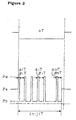
- Figure 2 is a view illustrating one embodiment of the irradiation pattern of a laser power during optical recording in the mark length modulation recording.
- the Figure illustrates an embodiment wherein an amorphous mark having a length nT, where T is a clock period, and n is a natural number of at least 2, is formed so that nT represents a mark length obtainable in the mark length modulation recording.
- bias power Pb of 0 ⁇ Pb ⁇ 0.5Pe is applied, (provided that when 2 ⁇ i ⁇ m-1, ⁇ i ⁇ i ).
- j is a parameter for shortening the application period of recording power to prevent an effect of heating by the final pulse.
- the medium of the present invention it is preferred to carry out recording/erasing by a three power level modulation wherein the above-mentioned off-pulse period is provided for bias power Pb, rather than by a two power level modulation with writing power Pw and erasing power Pe as heretofore employed in a conventional GeTe-Sb 2 Te 3 pseudo binary alloy system.
- Overwriting by the two power level modulation may be used, but by employing the three power level modulation system, the power margin and the linear velocity margin for recording can be broadened.
- bias power Pb for the off-pulse period it is particularly preferred to adjust bias power Pb for the off-pulse period to a sufficiently low level so that 0 ⁇ Pb ⁇ 0.5Pe.
- 0 ⁇ Pb ⁇ Pe is acceptable.
- erasing power Pe is a power which is capable of accomplishing recrystallization of amorphous mark portions
- writing power Pw is a power which is sufficient for melting the recording layer in a time of ⁇ i T and Pw>Pe.
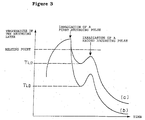
- Figure 3 is a schematic graph illustrating the temperature change of the recording layer when optical recording is carried out on the medium of the present invention.
- Pb during the off-pulse period is substantially 0, whereby the lowest temperature T Lb will be sufficiently lower than the melting point, and the cooling rate is high.
- the amorphous mark area is melted during irradiation with the first recording pulse and then is formed by quenching during the subsequent off-pulse period.
- the recording layer shows a high crystallization speed only in the vicinity of the melting point.
- the off-pulse is suitable, but such off-pulse is not necessarily suitable when applied to conventional GeTe-Sb 2 Te 3 type recording layer or when the recording layer of the present invention is applied to the mark position recording as shown in Examples of JP-A-1-303643.
- composition and the multilayer structure of the medium of the present invention represent indispensable improvements to make the alloy close to the Sb 70 Te 30 eutectic composition useful for a practical phase-change medium.
- the present invention is very important also from the viewpoint that the composition which used to be considered difficult to initialize and impractical as a recording layer, has been found to be suitable for high density recording once it has been initialized.
- composition of the recording layer of the second aspect of the present invention is the one having a predetermined amount of Ge and a predetermined amount of Ag or Zn added to the same base close to the Sb 70 Te 30 eutectic composition as in the first aspect of the present invention.
- the most important merit of employing the material for the recording layer of the present invention is that it provides a high crystallization speed, and it is thereby possible to suppress a phenomenon such that coarse grains having a reflectivity different from the 'initialized state will form in the periphery of an amorphous mark or in the erased mark.
- composition of the recording layer of this invention is represented by the following formula. Namely, it is represented by Mb z Ge y (Sb x Te 1-x ) 1-y-z , where Mb is at least one member selected from Ag and Zn, 0.60 ⁇ x ⁇ 0.85, 0.01 ⁇ y ⁇ 0.20, and 0.01 ⁇ z ⁇ 0.15.
- Addition of Ge is effective particularly for improving the thermal stability of the amorphous state and for increasing the archival stability of recorded amorphous marks.
- an intermetallic compound composition such as Ge 1 Sb 4 Te 7 , Ge 1 Sb 2 Te 4 , Ge 2 Sb 2 Te 5 or GeTe, tends to undergo phase separation, and the composition is likely to change by repetitive overwriting, such being undesirable. More preferably, it is at most 15 atomic %. On the other hand, if it is less than 1 atomic %, no substantial effect of addition will be obtained.
- Ag and Zn may be employed alone or in combination in an amount of at least 1 atomic %, to facilitate initialization of the amorphous layer immediately after its formation. If it exceeds 15 atomic %, the effect for stabilizing amorphous bits obtainable by the addition of Ge tends to be lost. Further, the jitter of the recorded mark edge deteriorates probably due to precipitation of a new alloy phase, such being undesirable.
- the amount is at most 10 atomic %.
- the SbTe eutectic composition By adding Ge, Ag and Zn to the SbTe eutectic composition, it is possible to shorten the crystallization time in the after-mentioned initialization operation, while maintaining the archival stability of an amorphous mark.
- Ge, Ag and Zn the composition of matrix SbTe to form eutectic will shift from Sb 70 Te 30 to a level of Sb 60 Te 40 to Sb 65 Te 35 . Accordingly, the linear velocity dependency will be determined by the excess amount of Sb based on this composition.
- the excess amount of Sb may be increased as described above. However, if it is increased too much, the stability of the recorded amorphous marks tends to be impaired. Therefore, with respect to Sb x Te 1-x , 0.60 ⁇ x ⁇ 0.85, preferably 0.65 ⁇ x ⁇ 0.80.
- melt initialization is effective as in the case of the first aspect of the present invention.
- a crystallization accelerating layer may be formed.
- the medium of this second aspect of the present invention has a multilayer structure as shown in Figure 1, like the first aspect of the invention.
- the thickness of the phase-change type recording layer 3 is preferably from 15 to 30 nm. If the thickness is thinner than 15 nm, no adequate contrast tends to be obtainable, and the crystallization speed tends to be slow, whereby it will be difficult to carry out erasing of record in a short period of time. On the other hand, if it is thicker than 30 nm, the heat capacity tends to be large, and the recording sensitivity tends to be poor.
- the materials for the upper and lower protective layers 2 and 3 may be the same as in the first aspect of the present invention.
- the lower protective layer 2 is required to have a function of suppressing a heat deformation of a plastic substrate. Accordingly, the thickness is preferably at least 50 nm. On the other hand, if it exceeds 500 nm, cracking is likely to result due to an internal stress. Accordingly, the thickness is usually selected within this range, so that the reflectivity, the difference in reflectivity between before and after recording, and the phase difference will be proper levels taking into the light interference effect into consideration.
- the thickness of the upper protective layer 4 is preferably from 10 to 50 nm. The most important reason is that heat dissipation to the reflective layer 5 is most efficiently be carried out. By adopting a multilayer structure to accelerate the heat dissipation and to increase the cooling rate for resolidification of the recording layer, a high erasing ratio can be accomplished by high speed crystallization, while avoiding problems involved in recrystallization.
- the thickness of the upper protective layer is thicker than 50 nm, the time until the heat of the recording layer reaches the reflective layer, tends to be long, whereby the heat dissipating effect by the reflective layer may not effectively be obtained.
- the thermal conductivity of a thin layer of less than 100 nm is usually smaller by 2 to 3 orders of magnitude from the thermal conductivity of bulk and has no substantial difference. Accordingly, the thickness of the protective layer becomes an important factor.
- the upper protective layer is thinner than 10 nm, it is likely to break due to e.g. deformation during melting of the recording layer, such being undesirable. This is undesirable also from such a viewpoint that the heat dissipating effect tends to be too large, and the power required for recording tends to be unnecessarily large.
- the reflective layer is preferably made of a material having a large reflectivity, and for the recording layer of the present invention, it is preferred to employ a material which has a particularly high thermal conductivity, so that the heat dissipating effect can be expected even via the upper dielectric layer.
- a metal containing at least 90 atomic % of Au, Ag or Al is preferably employed.
- a small amount of e.g. Ta, Ti, Cr, Mo, Mg, V, Nb or Zr may be added.
- the thickness of the reflective layer is preferably at least 50 nm to completely reflect the incident light without transmission of light. If the thickness exceeds 500 nm, the productivity tends to be poor with no further improvement in the heat dissipating effect, and cracking is likely to result. Therefore, thickness is preferably at most 500 nm.
- the recording method as described in the first aspect of the present invention may preferably be used in combination. It is particularly preferred to employ it in a linear velocity range of 1 to 7 m/s. If the linear velocity is less than 1 m/s, recrystallization is likely, and if it is more than 7 m/s, no adequate erasing ratio tends to be obtained. More preferably, the linear velocity is from 2 to 7 m/s.
- a certain specific recording method is combined to a medium having the same multilayer structure as the recording medium according to the first aspect of the present invention, wherein the recording layer is Ge f (Sb d Te 1-d ) 1-f , where 0.60 ⁇ d ⁇ 0.85, and 0.01 ⁇ f ⁇ 0.20, and has a thickness of from 15 to 30 nm, the upper protective layer has a thickness of from 10 to 50 nm, and the reflective layer is made of a metal containing at least 90 atomic % of Au, Ag or Al and has a thickness of from 50 to 500 nm.
- composition of the recording layer according to the third aspect of the present invention is the one having a predetermined amount of Ge added to the same base close to the Sb 70 Te 30 eutectic composition as used in the first aspect of the invention.
- the most important merit of employing the recording material of this invention is that it has a high crystallization speed, and it is thereby possible to suppress a phenomenon such that coarse grains which are different in the reflectivity from the initialized state will form along the periphery of an amorphous mark or in an erased mark.
- composition of the recording layer of this invention is represented by the following formula. Namely, it is represented by Ge f (Sb d Te 1-d ) 1-f , where 0.60 ⁇ d ⁇ 0.85, and 0.01 ⁇ f ⁇ 0.20.
- Adding Ge is effective particularly for improving the thermal stability of the amorphous state and for increasing the archival stability of recorded amorphous marks.
- an intermetallic compound composition such as Ge 1 Sb 4 Te 7 , Ge 1 Sb 2 Te 4 , Ge 2 Sb 2 Te 5 or GeTe, tends to undergo phase separation, and the composition is likely to change by repetitive overwriting. More preferably, it is at most 15 atomic %. On the other hand, if it is less than 1 atomic %, no substantial effect of addition is obtainable.
- the amount of Ge added is less than 1 atomic %, no adequate effect is obtainable, and in some cases, the crystallization temperature tends to decrease. If the amount of Ge added, exceeds 20 atomic %, other stabilized phase such as GeTe tends to precipitate, whereby the high speed crystallization tends to be impaired, and the crystal particles tend to be coarse, whereby the outline of the amorphous mark tends to be vague, and the jitter tends to increase, such being undesirable. Further, the composition is likely to change due to repetitive overwriting.
- the amount is particularly preferably from 2 to 15 atomic %, in order to maintain good properties even after 10,000 times of repetitive overwriting.
- the composition for matrix SbTe to form eutectic will shift from Sb 70 Te 30 to a level of Sb 60 Te 40 to Sb 65 Te 35 . Accordingly, the linear velocity dependency will be determined by the excess amount of Sb based on this composition.
- the excess amount of Sb may be increased as described above. However, if it is increased too much, stability of recorded amorphous marks tends to be impaired. Accordingly, in the case of Sb d Te 1-d , 0.60 ⁇ d ⁇ 0.85, preferably 0.65 ⁇ d ⁇ 0.75.
- melt initialization is effective like in the first aspect of the invention.
- a crystallization accelerating layer may be formed.
- the medium of this invention has a multilayer structure as shown in Figure 1, like the first aspect of the invention.
- the thickness of the phase-change type recording layer 3 of this invention is preferably within a range of from 15 to 30 nm. If the thickness is thinner than 15 nm, no adequate contrast tends to be obtained, and the crystallization speed tends to be slow, whereby it will be difficult to erase the record in a short period of time. On the other hand, if it is thicker than 30 nm, the heat capacity tends to be large, and the recording sensitivity tends to be poor.
- the materials for the upper and lower protective layers 2 and 4 may be the same as used in the first aspect of the invention.
- the lower protective layer 2 is required a have a function of suppressing heat deformation of the plastic substrate. Accordingly, the thickness is preferably at least 50 nm. On the other hand, if it exceeds 500 nm, cracking is likely to result due to an inner stress, such being undesirable. Usually, the thickness will be selected within this range, so that the reflectivity, the difference in reflectivity between before and after recording, and the phase difference will be proper levels taking the light interference effect into consideration.
- the thickness of the upper protective layer is limited from 10 to 50 nm. The most important reason is such that heat dissipation to the reflective layer 5 is effectively conducted.
- By adopting a multilayer structure for accelerating heat dissipation and for improving the cooling rate for recrystallization of the recording layer it is possible to realize a high erasing ratio by high crystallization, while avoiding a problem of recrystallization.
- the thickness of the upper protective layer exceeds 50 nm, the time until the heat of the recording layer reaches the reflective layer tends to be long, whereby the heat dissipating effect by the reflective layer may not effectively be obtained.
- it is at most 30 nm.
- the thermal conductivity of a thin layer of less than 100 nm is usually smaller by 2 to 3 figures than the thermal conductivity of bulk and has no substantial difference. Accordingly, the thickness of the protective layer becomes an important factor.
- the upper protective layer is thinner than 10 nm, it is likely to break due to e.g. deformation during melting of the recording layer, such being undesirable. This is undesirable also from such a viewpoint that the heat dissipating effect tends to be too large, and the power required for recording tends to be unnecessarily large.
- the reflective layer is preferably made of a material having a high reflectivity.
- the recording layer of the present invention it is preferred to employ the one having a particularly high thermal conductivity, so that the heat dissipating effect can be expected even via the upper dielectric layer.
- a metal containing at least 90 atomic % of Au, Ag or Al is preferably employed.
- a small amount of Ta, Ti, Cr, Mo, Mg, V, Nb or Zr may be added.
- the thickness of the reflective layer is preferably at least 50 nm to completely reflect the incident light without transmission of light. If the thickness exceeds 50 nm, the productivity tends to be poor with no further improvement in the heat dissipating effect, and cracking is likely to result. Accordingly, thickness is preferably at most 500 nm.
- the present inventors have found it effective to provide a crystallization accelerating layer, whereby the initial crystallization can be completed in a short period of time.
- the crystallization accelerating layer serves as crystal nuclei to promote the crystallization, or that the structure in the as-deposited state of the recording layer formed on the crystallization accelerating layer is different from the case where no crystallization accelerating layer is present, whereby crystallization readily proceeds.
- the initial crystallization can be facilitated when the crystallization accelerating layer is formed below the recording layer, but the effect tends to be small when the crystallization accelerating layer is formed on the recording layer. This indicates that the effect of the latter reason is predominant.
- the crystallization accelerating layer may be made of a readily crystallizable metal such as Au, Ag, Cu or Al, but is preferably the one having a refractive index which is close to the recording layer. Therefore, for the recording layer of the composition of the present invention, the crystallization accelerating layer is preferably of a composition close to Sb 2 Te 3 .
- composition close to Sb 2 Te 3 is, in many cases, crystalline even in the as-deposited state and likely to form crystal nuclei during the initial crystallization, and it also has a merit that it makes the as-deposited state of the recording layer formed thereon a readily crystallizable state.
- compositional range of the crystallization accelerating layer of Sb a Te 1-a is preferably 0.3 ⁇ a ⁇ 0.5, more preferably 0.35 ⁇ a ⁇ 0.45. Further, an additional element may be incorporated in an amount of at most 10 atomic%. For example, Ge 1 Sb 4 Te 7 or the like is useful for the crystallization accelerating layer.
- the crystallization accelerating layer provided at the time of forming the recording layer is considered to be mixed with other portions of the recording layer.
- the thickness of the crystallization accelerating layer is preferably at least 0.2 nm, more preferably at least 1 nm, and preferably at most 10 nm, more preferably at most 5 nm.
- composition-adjusting layer in contact with the crystallization accelerating layer so that the composition obtained by averaging the compositions of the crystallization accelerating layer and the composition-adjusting layer would be close to the composition of the recording layer.
- cosputtering was carried out by means of at least two types of targets i.e. a Zn 5 In 5 Sb 60 Te 30 , Zn 5 In 3 Sb 62 Te 30 or Zn 7 In 5 Sb 58 Te 30 alloy target, and a metal or alloy target such as Sb, Zn, InSb or ZnSb.
- targets i.e. a Zn 5 In 5 Sb 60 Te 30 , Zn 5 In 3 Sb 62 Te 30 or Zn 7 In 5 Sb 58 Te 30 alloy target, and a metal or alloy target such as Sb, Zn, InSb or ZnSb.
- cosputtering was carried out by means of at least two types of targets i.e. a Zn 5 In 3 Ge 3 Sb 59 Te 30 , Zn 5 In 7 Ge 5 Sb 53 Te 30 or Zn 7 In 5 Sb 58 Te 30 alloy target, and a metal or alloy target, such as Sb, Ge, Zn, InSb or ZnSb.
- targets i.e. a Zn 5 In 3 Ge 3 Sb 59 Te 30 , Zn 5 In 7 Ge 5 Sb 53 Te 30 or Zn 7 In 5 Sb 58 Te 30 alloy target, and a metal or alloy target, such as Sb, Ge, Zn, InSb or ZnSb.
- cosputtering was carried out by means of at least three types of targets i.e. a Ge 1 Sb 2 Te 4 or Ge 2 Sb 2 Te 5 ternary alloy target, Sb, and Ag or Zn.
- the composition was adjusted.
- the composition of the obtained thin alloy layer was measured by X-ray fluorescence intensity corrected by chemical analysis.
- a (ZnS) 80 (SiO 2 ) 20 layer 85 nm of a (ZnS) 80 (SiO 2 ) 20 layer, 20 nm of a Zn 5 In 5 Sb 60 Te 30 as a recording layer, 20 nm of a (ZnS) 80 (SiO 2 ) 20 layer and 170 nm of a Al 98.5 Ta 1.5 alloy layer, were sequentially laminated by magnetron sputtering, and an ultraviolet ray-curable resin was further coated in a thickness of 4 ⁇ m to obtain a disk.
- This optical disk was subjected to melt initialization at a linear velocity of 3.5 m/s at a beam-transferring speed (in the radial direction of the disk) of 50 ⁇ m/rotation with a laser power of 550 mW by means of an optical disk initialization apparatus with an elliptic irradiation beam having a long axis of 80 ⁇ m and a short axis of about 1.4 ⁇ m, whereby initial crystallization was carried out by one scanning operation.
- EFM random signals (clock period: 115 nsec) were recorded at a linear velocity of 2.4 m/s by means of an optical disk evaluation apparatus (laser wavelength: 780 mm, NA: 0.55).
- the jitter value showing the actual signal characteristic was less than 10% of the clock period with the shortest mark length and thus showed a good result. Further, this characteristic was maintained even after 1,000 times of overwriting. Further, the recorded signals showed no deterioration even after being left for 1,000 hours in an environment wherein the temperature was 80°C and the relative humidity was 80%.
- a (ZnS) 80 (SiO 2 ) 20 layer On a polycarbonate substrate, 80 nm of a (ZnS) 80 (SiO 2 ) 20 layer, 20 nm of a Zn 7 In 5 Sb 58 Te 30 as a recording layer, 20 nm of a (ZnS) 80 (SiO 2 ) 20 layer and 170 nm of a Al 98.5 Ta 1.5 alloy layer, were sequentially laminated by magnetron sputtering, and an ultraviolet ray-curable resin was further coated in a thickness of 4 ⁇ m to obtain a disk.
- a (ZnS) 80 (SiO 2 ) 20 layer On a polycarbonate substrate, 80 nm of a (ZnS) 80 (SiO 2 ) 20 layer, 20 nm of a Zn 7 In 5 Sb 58 Te 30 as a recording layer, 20 nm of a (ZnS) 80 (SiO 2 ) 20 layer and 170 n
- This optical disk was subjected to melt initialization at a linear speed of 3.5 m/s at a beam-transferring speed (in the radial direction of the disk) of 50 ⁇ m/rotation with a laser power of 550 mW by means of the same optical disk initialization apparatus as used in Example 1 by irradiating an elliptic light beam with a long axis of 80 ⁇ m and a short axis of about 1.4 ⁇ m, whereby the initial crystallization was carried out by one scanning operation.
- the jitter value showing the actual signal characteristic was less than 10% of the clock period with the shortest mark length and thus showed a good result. Further, this characteristic was maintained even after 1,000 times of overwriting. Further, the recorded signals showed no deterioration even after being left for 1,000 hours in an environment in which the temperature was 80°C and the relative humidity was 80%.
- a (ZnS) 80 (SiO 2 ) 20 layer On a polycarbonate substrate, 80 nm of a (ZnS) 80 (SiO 2 ) 20 layer, 20 nm of a Zn 5 In 3 Ge 3 Sb 59 Te 30 layer as a recording layer, 20 nm of a (ZnS) 80 (SiO 2 ) 20 layer and 170 nm of a Al 98.5 Ta 1.5 alloy layer, were sequentially laminated by magnetron sputtering, and an ultraviolet ray-curable resin was further coated in a thickness of 4 ⁇ m to obtain a disk.
- a (ZnS) 80 (SiO 2 ) 20 layer On a polycarbonate substrate, 80 nm of a (ZnS) 80 (SiO 2 ) 20 layer, 20 nm of a Zn 5 In 3 Ge 3 Sb 59 Te 30 layer as a recording layer, 20 nm of a (ZnS) 80 (SiO 2 ) 20
- This optical disk was subjected to melt initialization at a linear velocity of 3 m/s at a beam-transferring speed (in the radial direction of the disk) of 50 ⁇ m/rotation with a laser power of 600 mW by means of the same optical disk initialization apparatus as used in Example 1, whereby initial crystallization was carried out by one scanning operation.
- the jitter value showing the actual signal characteristic was less than 10% of the clock period with the shortest mark length and thus showed a good result. Further, this characteristic was maintained even after 2,000 times of overwriting. Further, the recorded signals showed no deterioration even after being left for 1,000 hours in an environment wherein temperature was 80°C and the relative humidity was 80%.
- a (ZnS) 80 (SiO 2 ) 20 layer On a polycarbonate substrate, 80 nm of a (ZnS) 80 (SiO 2 ) 20 layer, 20 nm of a Zn 7 In 3 Ge 3 Sb 58 Te 29 layer as a recording layer, 20 nm of a (ZnS) 80 (SiO 2 ) 20 layer and 200 nm of a Al 98.0 Ta 2.0 alloy layer, were sequentially laminated by magnetron sputtering, and an ultraviolet ray-curable resin was further coated in a thickness of 4 ⁇ m to obtain a disk.
- a (ZnS) 80 (SiO 2 ) 20 layer On a polycarbonate substrate, 80 nm of a (ZnS) 80 (SiO 2 ) 20 layer, 20 nm of a Zn 7 In 3 Ge 3 Sb 58 Te 29 layer as a recording layer, 20 nm of a (ZnS) 80 (SiO 2 ) 20 layer
- This optical disk was subjected to melt initialization at a linear velocity of 3 m/s at a beam-transferring speed (in the radial direction of the disk) of 50 ⁇ m/rotation with a laser power of 600 mW by means of the same optical disk initialization apparatus as used in Example 1, whereby initial crystallization was carried out by one scanning operation.
- the jitter value showing the actual signal characteristic was less than 10% of the clock period with the shortest mark length and thus showed a good result. Further, this characteristic was maintained even after 2,000 times of overwriting. Further, the recorded signals showed no deterioration after being left for 1,000 hours in an environment in which the temperature was 80°C and the relative humidity was 80%.
- a (ZnS) 80 (SiO 2 ) 20 layer On a polycarbonate substrate, 80 nm of a (ZnS) 80 (SiO 2 ) 20 layer, 20 nm of a Zn 5 In 10 Sb 60 Te 25 layer as a recording layer, 20 nm of a (ZnS) 80 (SiO 2 ) 20 layer and 200 nm of a Al 98.0 Ta 2.0 alloy layer, were sequentially laminated by magnetron sputtering, and an ultraviolet ray-curable resin was further coated in a thickness of 4 ⁇ m to obtain a disk.
- a (ZnS) 80 (SiO 2 ) 20 layer On a polycarbonate substrate, 80 nm of a (ZnS) 80 (SiO 2 ) 20 layer, 20 nm of a Zn 5 In 10 Sb 60 Te 25 layer as a recording layer, 20 nm of a (ZnS) 80 (SiO 2 ) 20 layer and 200 nm of
- This optical disk was subjected to melt initialization at a linear velocity of 3 m/s at a beam-transferring speed (in the radial direction of the disk) of 50 ⁇ m/rotation with a laser power of 600 mW by means of the same optical disk initialization apparatus as used in Example 1, whereby initial crystallization was carried out by one scanning operation.
- the jitter value showing the actual signal characteristic was less than 10% of the clock period with the shortest mark length, and the initial characteristic was good. However, after 1,000 times of overwriting, the jitter increased abruptly. Especially, a long mark such as 11T was observed to remain without being completely erased. It is considered that since In was contained in a large amount, segregation resulted, whereby recrystallization (erasing) was hindered.
- a (ZnS) 80 (SiO 2 ) 20 layer On a polycarbonate substrate, 80 nm of a (ZnS) 80 (SiO 2 ) 20 layer, 20 nm of a Zn 5 In 2 Sb 62 Te 31 layer as a recording layer, 20 nm of a (ZnS) 80 (SiO 2 ) 20 layer and 200 nm of a Al 98.0 Ta 2.0 alloy layer, were sequentially laminated by magnetron sputtering, and an ultraviolet ray-curable resin was further coated in a thickness of 4 ⁇ m to obtain a disk.
- a (ZnS) 80 (SiO 2 ) 20 layer On a polycarbonate substrate, 80 nm of a (ZnS) 80 (SiO 2 ) 20 layer, 20 nm of a Zn 5 In 2 Sb 62 Te 31 layer as a recording layer, 20 nm of a (ZnS) 80 (SiO 2 ) 20 layer and 200 n
- This optical disk was subjected to melt initialization at a linear velocity of 3 m/s at a beam-transferring speed (in the radial direction of the disk) of 50 ⁇ m/rotation with a laser power of 500 mW by means of the same optical disk initialization apparatus as used in Example 1, whereby initial crystallization was carried out by one scanning operation.
- the jitter value showing the actual signal characteristic was less than 10% of the clock period with the shortest mark length, and the initial characteristic was good. Further, even after 1,000 times of overwriting, the jitter was still less than 10% of the clock period and thus showed a good result. However, recorded signals deteriorated when it was left for 500 hours in an environment wherein the temperature was 80°C and the relative humidity was 80%, and the jitter reached 20% of the clock period.
- a (ZnS) 80 (SiO 2 ) 20 layer On a polycarbonate substrate, 80 nm of a (ZnS) 80 (SiO 2 ) 20 layer, 20 nm of a Zn 15 In 5 Sb 51 Te 29 layer as a recording layer, 20 nm of a (ZnS) 80 (SiO 2 ) 20 layer and 170 nm of a Al 98.5 Ta 1.5 alloy layer, were sequentially laminated by magnetron sputtering, and an ultraviolet ray-curable resin was further coated in a thickness of 4 ⁇ m to obtain a disk.
- a (ZnS) 80 (SiO 2 ) 20 layer On a polycarbonate substrate, 80 nm of a (ZnS) 80 (SiO 2 ) 20 layer, 20 nm of a Zn 15 In 5 Sb 51 Te 29 layer as a recording layer, 20 nm of a (ZnS) 80 (SiO 2 ) 20 layer and 170 n
- This optical disk was subjected to melt initialization at a linear velocity of 3 m/s at a beam-transferring speed (in the radial direction of the disk) of 50 ⁇ m/rotation with a laser power of 600 mW by means of the same optical disk initialization apparatus as used in Example 1, whereby initial crystallization was carried out by one scanning operation.
- the jitter value was slightly high at a level of 15% of the clock period with the shortest mark length. Besides, after 1,000 times of overwriting, the jitter remarkably increased to a level of at least 20% of the clock period.
- a (ZnS) 80 (SiO 2 ) 20 layer On a polycarbonate substrate, 80 nm of a (ZnS) 80 (SiO 2 ) 20 layer, 20 nm of a Zn 13 In 5 Ge 3 S 52 Te 27 layer as a recording layer, 20 nm of a (ZnS) 80 (SiO 2 ) 20 layer and 170 nm of a Al 98.5 Ta 1.5 alloy layer, were sequentially laminated by magnetron sputtering, and an ultraviolet ray-curable resin was further coated in a thickness of 4 ⁇ m to obtain a disk.
- a (ZnS) 80 (SiO 2 ) 20 layer On a polycarbonate substrate, 80 nm of a (ZnS) 80 (SiO 2 ) 20 layer, 20 nm of a Zn 13 In 5 Ge 3 S 52 Te 27 layer as a recording layer, 20 nm of a (ZnS) 80 (SiO 2 ) 20 layer and 170
- This optical disk was subjected to melt initialization at a linear velocity of 3.5 m/s at a beam-transferring speed (in the radial direction of the disk) of 50 ⁇ m/rotation with a laser power of 550 mW by means of the same optical disk initialization apparatus as used in Example 1, whereby initial crystallization was carried out by one scanning operation.
- the jitter value was slightly high at a level of 15% of the clock period with the shortest mark length. Besides, after 1,000 times of overwriting, the jitter remarkably increased to a level of at least 20% of the clock period.
- a (ZnS) 80 (SiO 2 ) 20 layer On a polycarbonate substrate, 80 nm of a (ZnS) 80 (SiO 2 ) 20 layer, 20 nm of a Ag 5 In 3 Sb 62 Te 30 layer as a recording layer, 20 nm of a (ZnS) 80 (SiO 2 ) 20 layer and 170 nm of a Al 98.5 Ta 1.5 alloy layer, were sequentially laminated by magnetron sputtering, and an ultraviolet ray-curable resin was further coated in a thickness of 4 ⁇ m to obtain a disk.
- a (ZnS) 80 (SiO 2 ) 20 layer On a polycarbonate substrate, 80 nm of a (ZnS) 80 (SiO 2 ) 20 layer, 20 nm of a Ag 5 In 3 Sb 62 Te 30 layer as a recording layer, 20 nm of a (ZnS) 80 (SiO 2 ) 20 layer and 170 n
- This optical disk was subjected to melt initialization at a linear velocity of 3.5 m/s at a beam-transferring speed (in the radial direction of the disk) of 10 ⁇ m/rotation with a laser power of 550 mW by means of the same optical disk initialization apparatus as used in Example 1, whereby initial crystallization was carried out by one scanning operation.
- the jitter value showing the actual signal characteristic was less than 10% of the clock period with the shortest mark length, and the initial characteristic was good. Further, even after 1,000 times of overwriting, this characteristic was maintained. However, the recorded signals deteriorated when they were left for 1,000 hours in an environment in which the temperature was 80°C and the relative humidity was 80%, and the jitter reached to 20% of the clock period. It was found that amorphous bits partially underwent recrystallization and thus were partly erased.
- a (ZnS) 80 (SiO 2 ) 20 layer On a polycarbonate substrate, 230 nm of a (ZnS) 80 (SiO 2 ) 20 layer, 20 nm of a Ag 6 Ge 5 Sb 70 Te 19 layer as a recording layer, 20 nm of a (ZnS) 80 (SiO 2 ) 20 layer and 200 nm of a Al 97.5 Ta 2.5 alloy layer, were sequentially laminated by magnetron sputtering, and an ultraviolet ray-curable resin layer was further formed in a thickness of 4 ⁇ m to obtain an optical disk.
- a (ZnS) 80 (SiO 2 ) 20 layer On a polycarbonate substrate, 230 nm of a (ZnS) 80 (SiO 2 ) 20 layer, 20 nm of a Ag 6 Ge 5 Sb 70 Te 19 layer as a recording layer, 20 nm of a (ZnS) 80 (SiO 2 ) 20 layer and 200 nm
- This optical disk was subjected to melt initialization at a linear velocity of 4.5 m/s at a beam-transferring speed of 5 ⁇ m/rotation with a laser power of 250 mW by means of an optical disk initialization apparatus with an elliptic irradiation beam with a long axis of 50 ⁇ m, whereby the initial crystallization was carried out.
- EFM random signals (clock period: 115 nsec) were recorded at a linear velocity of 2.8 m/s by means of an optical disk evaluation apparatus (laser wavelength: 780 nm, NA: 0.55).
- laser wavelength: 780 nm, NA: 0.55 laser wavelength: 780 nm, NA: 0.55
- the jitter value showing the actual signal characteristic was less than 10% of the clock period with the shortest mark length and thus showed a good result. Further, this characteristic was maintained even after 1,000 times of overwriting.
- the recorded signals showed no deterioration even after being left for 1,000 hours in an environment in which the temperature was 80°C and the relative humidity was 80%.
- a (ZnS) 80 (SiO 2 ) 20 layer On a polycarbonate substrate, 230 nm of a (ZnS) 80 (SiO 2 ) 20 layer, 20 nm of a Ag 10 Ge 7 Sb 66 Te 17 layer as a recording layer, 20 nm of a (ZnS) 80 (SiO 2 ) 20 layer and 200 nm of a Al 97.5 Ta 2.5 alloy layer, were sequentially laminated by magnetron sputtering, and an ultraviolet ray-curable resin layer was further formed in a thickness of 4 ⁇ m to obtain an optical disk.
- a (ZnS) 80 (SiO 2 ) 20 layer On a polycarbonate substrate, 230 nm of a (ZnS) 80 (SiO 2 ) 20 layer, 20 nm of a Ag 10 Ge 7 Sb 66 Te 17 layer as a recording layer, 20 nm of a (ZnS) 80 (SiO 2 ) 20 layer and 200
- This optical disk was subjected to melt initialization under the same conditions as in Example 5, whereby initial crystallization was carried out.
- the jitter value showing the actual signal characteristic was less than 10% of the clock period with the shortest mark length and thus showed a good result. Further, this characteristic was maintained even after 1,000 times of overwriting.
- the recorded signals showed no deterioration even after being left for 1,000 hours in an environment in which the temperature was 80°C and the relative humidity was 80%.
- a (ZnS) 80 (SiO 2 ) 20 layer On a polycarbonate substrate, 230 nm of a (ZnS) 80 (SiO 2 ) 20 layer, 20 nm of a Zn 6 Ge 7 Sb 60 Te 27 layer as a recording layer, 20 nm of a (ZnS) 80 (SiO 2 ) 20 layer and 200 nm of a Al 97.5 Ta 2.5 alloy layer, were sequentially laminated by magnetron sputtering, and an ultraviolet ray-curable resin layer was further formed in a thickness of 4 ⁇ m to obtain an optical disk.
- a (ZnS) 80 (SiO 2 ) 20 layer On a polycarbonate substrate, 230 nm of a (ZnS) 80 (SiO 2 ) 20 layer, 20 nm of a Zn 6 Ge 7 Sb 60 Te 27 layer as a recording layer, 20 nm of a (ZnS) 80 (SiO 2 ) 20 layer and 200
- This optical disk was subjected to melt initialization under the same conditions as in Example 5, whereby initial crystallization was carried out.
- the jitter value showing the actual signal characteristic was less than 10% of the clock period with the shortest mark length and thus showed a good result. Further, this characteristic was maintained even after 1,000 times of overwriting.
- the recorded signals showed no deterioration even after being left for 1,000 hours in an environment in which the temperature was 80°C and the relative humidity was 80%.
- a (ZnS) 80 (SiO 2 ) 20 layer On a polycarbonate substrate, 230 nm of a (ZnS) 80 (SiO 2 ) 20 layer, 20 nm of a Zn 3 Ge 3 Sb 61 Te 28 layer as a recording layer, 20 nm of a (ZnS) 80 (SiO 2 ) 20 layer and 200 nm of a Al 97.5 Ta 2.5 alloy layer, were sequentially laminated by magnetron sputtering, and an ultraviolet ray-curable resin layer was further formed in a thickness of 4 ⁇ m to obtain an optical disk.
- a (ZnS) 80 (SiO 2 ) 20 layer On a polycarbonate substrate, 230 nm of a (ZnS) 80 (SiO 2 ) 20 layer, 20 nm of a Zn 3 Ge 3 Sb 61 Te 28 layer as a recording layer, 20 nm of a (ZnS) 80 (SiO 2 ) 20 layer and
- This optical disk was subjected to a first step of initialization crystallization at a linear velocity of 4.5 m/s at a beam-transferring speed of 5 ⁇ m/rotation with a laser power of 300 mW by means of the same optical disk initialization apparatus as used in Example 5 to increase the reflectivity to a level of 80% of the final crystalline state, and further subjected to irradiation once with 11 mW by the following tester, whereby melt initial crystallization was carried out. It is regarded that so long as initialization can be completed by irradiation of twice of this level, there will be no problem from the industrial point of view.
- the jitter value showing the actual signal characteristic was less than 10% of the clock period with the shortest mark length and thus showed a good result. Further, this characteristic was maintained even after 1,000 times of overwriting.
- the recorded signals showed no deterioration even after being left for 1,000 hours in an environment in which the temperature was 80°C and the relative humidity was 80%.
- a (ZnS) 80 (SiO 2 ) 20 layer On a polycarbonate substrate, 230 nm of a (ZnS) 80 (SiO 2 ) 20 layer, 20 nm of a Zn 6 Ge 7 Sb 62 Te 25 layer as a recording layer, 20 nm of a (ZnS) 80 (SiO 2 ) 20 layer and 200 nm of a Al 97.5 Ta 2.5 alloy layer, were sequentially laminated by magnetron sputtering, and an ultraviolet ray-curable resin layer was further formed in a thickness of 4 ⁇ m to obtain an optical disk.
- a (ZnS) 80 (SiO 2 ) 20 layer On a polycarbonate substrate, 230 nm of a (ZnS) 80 (SiO 2 ) 20 layer, 20 nm of a Zn 6 Ge 7 Sb 62 Te 25 layer as a recording layer, 20 nm of a (ZnS) 80 (SiO 2 ) 20 layer and
- This optical disk was subjected to melt initialization under the same conditions as in Example 5, whereby initial crystallization was carried out.
- EFM random signals (clock period: 115 nsec) were recorded at a linear velocity of 2.8 m/s by means of an optical disk evaluation apparatus (laser wavelength: 780 nm, NA: 0.55).
- laser wavelength: 780 nm, NA: 0.55 laser wavelength: 780 nm, NA: 0.55
- the jitter value showing the actual signal characteristic was less than 10% of the clock period with the shortest mark length and thus showed a good result. Further, this characteristic was maintained even after 1,000 times of overwriting.
- the recorded signals showed no deterioration even after being left for 500 hours in an environment in which the temperature was 80°C and the relative humidity was 80%.
- a (ZnS) 80 (SiO 2 ) 20 layer On a polycarbonate substrate, 230 nm of a (ZnS) 80 (SiO 2 ) 20 layer, 20 nm of a Ag 5 Sb 66 Te 29 layer as a recording layer, 20 nm of a (ZnS) 80 (SiO 2 ) 20 layer and 200 nm of a Al 97.5 Ta 2.5 alloy layer, were sequentially laminated by magnetron sputtering, and an ultraviolet ray-curable resin layer was further formed in a thickness of 4 ⁇ m to obtain an optical disk.
- a (ZnS) 80 (SiO 2 ) 20 layer On a polycarbonate substrate, 230 nm of a (ZnS) 80 (SiO 2 ) 20 layer, 20 nm of a Ag 5 Sb 66 Te 29 layer as a recording layer, 20 nm of a (ZnS) 80 (SiO 2 ) 20 layer and 200 nm of
- This optical disk was subjected to melt initialization under the same conditions as in Example 5, whereby initial crystallization was carried out.
- the jitter value showing the actual signal characteristic was less than 10% of the clock period with the shortest mark length, and thus the initial characteristic was good. Further, this characteristic was maintained even after 1,000 times of overwriting.
- the recorded signals deteriorated after being left for 500 hours in an environment in which the temperature was 80°C and a relative humidity was 80%, and the jitter reached 20% of the clock period. It was found that amorphous bits were partially recrystallized and partially erased.
- a (ZnS) 80 (SiO 2 ) 20 layer On a polycarbonate substrate, 230 nm of a (ZnS) 80 (SiO 2 ) 20 layer, 1 nm of a Sb 2 Te 3 layer as a crystallization accelerating layer, 1 nm of Sb layer as a composition-adjusting layer, 18 nm of a Ge 10 Sb 67 Te 23 layer as a recording layer, 20 nm of a (ZnS) 80 (SiO 2 ) 20 layer and 100 nm of a Al 97.5 Ta 2.5 alloy layer, were sequentially laminated by magnetron sputtering, and an ultraviolet ray-curable resin layer was further formed in a thickness of 4 ⁇ m to obtain an optical disk.
- a (ZnS) 80 (SiO 2 ) 20 layer On a polycarbonate substrate, 230 nm of a (ZnS) 80 (SiO 2 ) 20 layer, 1 nm of a Sb 2 Te 3
- This optical disk was subjected to melt initial crystallization at a disk rotational speed of 2,700 rpm at a beam-transferring speed of 5 ⁇ m/rotation with a laser power of 400 mW with a radius of 64 mm and a laser power of 170 mW with a radius of 27 mm by means of an optical disk initialization apparatus with an elliptic irradiation beam having a long axis of about 50 ⁇ m, whereby initial crystallization was carried out.
- EFM random signals (clock period: 115 nsec) were recorded at a linear velocity of 2.8 m/s by means of an optical disk evaluation apparatus (laser wavelength: 780 nm, NA: 0.55).
- laser wavelength: 780 nm, NA: 0.55 laser wavelength: 780 nm, NA: 0.55
- the jitter value showing the actual signal characteristic was less than 10% of the clock period with the shortest mark length and thus showed a good result, and this characteristic was maintained even after 1,000 times of overwriting.
- the recorded signals showed no deterioration even after being left for 2,000 hours in an environment in which the temperature was 80°C and a relative humidity was 80%.
- a (ZnS) 80 (SiO 2 ) 20 layer On a polycarbonate substrate, 230 nm of a (ZnS) 80 (SiO 2 ) 20 layer, 1 nm of a Sb 2 Te 3 layer as a crystallization accelerating layer, 19 nm of a Ge 10 Sb 67 Te 23 layer as a recording layer, 20 nm of a (ZnS) 80 (SiO 2 ) 20 layer and 100 nm of a Al 97.5 Ta 2.5 alloy layer, were sequentially laminated by magnetron sputtering, and an ultraviolet ray-curable resin layer was further formed in a thickness of 4 ⁇ m to obtain an optical disk.
- a (ZnS) 80 (SiO 2 ) 20 layer On a polycarbonate substrate, 230 nm of a (ZnS) 80 (SiO 2 ) 20 layer, 1 nm of a Sb 2 Te 3 layer as a crystallization accelerating layer, 19 nm of
- This disk was subjected to initialization under the same conditions as in Example 10, whereby initialization was carried out.
- the jitter value showing the actual signal characteristic was less than 10% of the clock period with the shortest mark length and thus showed a good result. This characteristic was maintained even after 1,000 times of overwriting.
- the recorded signals showed no deterioration even after being left for 2,000 hours in an environment in which the temperature was 80°C, and the relative humidity was 80%.
- a (ZnS) 80 (SiO 2 ) 20 layer On a polycarbonate substrate, 230 nm of a (ZnS) 80 (SiO 2 ) 20 layer, 20 nm of a Ge 10 Sb 67 Te 23 layer as a recording layer, 20 nm of a (ZnS) 80 (SiO 2 ) 20 layer and 100 nm of a Al 97.5 Ta 2.5 alloy layer, were sequentially laminated by magnetron sputtering, and an ultraviolet ray-curable resin layer was further formed in a thickness of 4 ⁇ m to obtain an optical disk.
- a (ZnS) 80 (SiO 2 ) 20 layer On a polycarbonate substrate, 230 nm of a (ZnS) 80 (SiO 2 ) 20 layer, 20 nm of a Ge 10 Sb 67 Te 23 layer as a recording layer, 20 nm of a (ZnS) 80 (SiO 2 ) 20 layer and 100 nm of
- melt initial crystallization was carried out by irradiating a DC laser beam many times to every track by means of an optical disk evaluation apparatus.
- the jitter value showing the actual signal-characteristic was less than 10% of the clock period with the shortest mark length and thus showed a good result. This characteristic was maintained even after 1,000 times of overwriting.
- the recorded signals showed no deterioration even after being left for 2,000 hours in an environment in which the temperature was 80°C, and the relative humidity was 80%.
- a (ZnS) 80 (SiO 2 ) 20 layer On a polycarbonate substrate, 80 nm of a (ZnS) 80 (SiO 2 ) 20 layer, 20 nm of a Ge 12 Sb 66 Te 22 layer as a recording layer, 20 nm of a (ZnS) 80 (SiO 2 ) 20 layer and 200 nm of a Al 98.5 Ta 1.5 alloy layer, were sequentially laminated by magnetron sputtering, and an ultraviolet ray-curable resin was further coated in a thickness of 4 ⁇ m to obtain a disk.
- a (ZnS) 80 (SiO 2 ) 20 layer On a polycarbonate substrate, 80 nm of a (ZnS) 80 (SiO 2 ) 20 layer, 20 nm of a Ge 12 Sb 66 Te 22 layer as a recording layer, 20 nm of a (ZnS) 80 (SiO 2 ) 20 layer and 200 nm of a Al 9
- This optical disk was subjected to initial crystallization at a linear speed of from 2.0 to 5.0 m/s at a beam-transferring rate (in the radial direction of the disk) of from 10 to 50 ⁇ m/rotation with a laser power of from 500 to 900 mW by means of the same optical disk initialization apparatus as used in Example 1, whereby initial crystallization was incomplete and non-uniform. With a power of at least 800 mW, defects resulted due to deterioration by heat. Therefore, melt initial crystallization was carried out by irradiating a DC laser beam many times to every track by means of an optical disk evaluation apparatus.
- the jitter value showing the actual signal characteristic was less than 10% of the clock period with the shortest mark length and thus showed a good result. This characteristic was maintained even after 1,000 times of overwriting.
- the recorded signals showed no deterioration even after being left for 2,000 hours in an environment. in which the temperature was 80°C, and the relative humidity was 80%.
- a (ZnS) 80 (SiO 2 ) 20 layer On a polycarbonate substrate, 230 nm of a (ZnS) 80 (SiO 2 ) 20 layer, 20 nm of a Ge 10 Sb 67 Te 23 layer as a recording layer, 20 nm of a (ZnS) 80 (SiO 2 ) 20 layer and 200 nm of a Al 97.5 Ta 2.5 alloy layer, were sequentially laminated by magnetron sputtering, and an ultraviolet ray-curable resin layer was further formed in a thickness of 4 ⁇ m to obtain an optical disk.
- a (ZnS) 80 (SiO 2 ) 20 layer On a polycarbonate substrate, 230 nm of a (ZnS) 80 (SiO 2 ) 20 layer, 20 nm of a Ge 10 Sb 67 Te 23 layer as a recording layer, 20 nm of a (ZnS) 80 (SiO 2 ) 20 layer and 200 nm of
- melt initial crystallization was carried out by irradiating a DC laser beam many times to every track by means of an optical disk evaluation apparatus.
- the jitter value showing the actual signal characteristic was less than 10% of the clock period with the shortest mark length and thus showed a good result. This characteristic was maintained even after 1,000 times of overwriting.
- the recorded signals showed no deterioration even after being left for 2,000 hours in an environment in which the temperature was 80°C, and the relative humidity was 80%.
- a (ZnS) 80 (SiO 2 ) 20 layer On a polycarbonate substrate, 230 nm of a (ZnS) 80 (SiO 2 ) 20 layer, 20 nm of a Ge 7 Sb 65 Te 28 layer as a recording layer, 20 nm of a (ZnS) 80 (SiO 2 ) 20 layer and 100 nm of a Al 97.5 Ta 2.5 alloy layer, were sequentially laminated by magnetron sputtering, and an ultraviolet ray-curable resin layer was further formed in a thickness of 4 ⁇ m to obtain an optical disk.
- a (ZnS) 80 (SiO 2 ) 20 layer On a polycarbonate substrate, 230 nm of a (ZnS) 80 (SiO 2 ) 20 layer, 20 nm of a Ge 7 Sb 65 Te 28 layer as a recording layer, 20 nm of a (ZnS) 80 (SiO 2 ) 20 layer and 100 nm of a Al
- melt initial crystallization was carried out by irradiating a DC laser beam many times to every track by an optical disk evaluation apparatus.
- the jitter value showing the actual signal characteristic was less than 10% of the clock period with the shortest mark length and thus showed a good result, and this characteristic was maintained even after 1,000 times of overwriting.
- the recorded signals showed no deterioration even after being left for 1,000 hours in an environment in which the temperature was 80°C, and the relative humidity was 80%.
- a (ZnS) 80 (SiO 2 ) 20 layer On a polycarbonate substrate, 230 nm of a (ZnS) 80 (SiO 2 ) 20 layer, 20 nm of a Sb 72 Te 28 layer as a recording layer, 20 nm of a (ZnS) 80 (SiO 2 ) 20 layer and 100 nm of a Al 97.5 Ta 2.5 alloy layer, were sequentially laminated by magnetron sputtering, and an ultraviolet ray-curable resin layer was further formed in a thickness of 4 ⁇ m to obtain an optical disk.
- a (ZnS) 80 (SiO 2 ) 20 layer On a polycarbonate substrate, 230 nm of a (ZnS) 80 (SiO 2 ) 20 layer, 20 nm of a Sb 72 Te 28 layer as a recording layer, 20 nm of a (ZnS) 80 (SiO 2 ) 20 layer and 100 nm of a Al 97.5 Ta 2.5
- melt initial crystallization was carried out by irradiating a DC laser beam many times to every track by an optical disk evaluation apparatus.
- the jitter value showing the actual signal characteristic was less than 10% of the clock period with the shortest mark length and thus showed a good result, and this characteristic was maintained even after 1,000 times of overwriting.
- the recorded signals deteriorated after being left for 500 hours in an environment in which the temperature was 80°C, and the relative humidity was 80%, and it was impossible to readout the signals.
- a (ZnS) 80 (SiO 2 ) 20 layer On a polycarbonate substrate, 230 nm of a (ZnS) 80 (SiO 2 ) 20 layer, 20 nm of a Ge 21 Sb 61 Te 18 layer as a recording layer, 20 nm of a (ZnS) 80 (SiO 2 ) 20 layer and 100 nm of a Al 97.5 Ta 2.5 alloy layer, were sequentially laminated by magnetron sputtering, and an ultraviolet ray-curable resin layer was further formed in a thickness of 4 ⁇ m to obtain an optical disk.
- a (ZnS) 80 (SiO 2 ) 20 layer On a polycarbonate substrate, 230 nm of a (ZnS) 80 (SiO 2 ) 20 layer, 20 nm of a Ge 21 Sb 61 Te 18 layer as a recording layer, 20 nm of a (ZnS) 80 (SiO 2 ) 20 layer and 100 nm of
- melt initial crystallization was carried out by irradiating a DC laser beam many times to every track by an optical disk evaluation apparatus.
- the jitter value showing the actual signal characteristic was at least 10% of the clock period with the shortest mark length, and thus no good characteristic was obtained.
- the present invention it is possible to provide an optical recording medium which has excellent archival stability and high durability in repetitive overwriting and has a low jitter in high density mark length recording. Further, by using such a recording medium in combination with the optical recording method of the present invention, mark length recording of higher precision can be realized.
Landscapes
- Physics & Mathematics (AREA)
- Optics & Photonics (AREA)
- Chemical & Material Sciences (AREA)
- Inorganic Chemistry (AREA)
- Engineering & Computer Science (AREA)
- Manufacturing & Machinery (AREA)
- Thermal Transfer Or Thermal Recording In General (AREA)
- Optical Record Carriers And Manufacture Thereof (AREA)
Priority Applications (1)
| Application Number | Priority Date | Filing Date | Title |
|---|---|---|---|
| EP05025175A EP1630803B1 (de) | 1996-10-04 | 1997-10-02 | Medium für optische Datenaufzeichnung und optisches Aufzeichnungsverfahren |
Applications Claiming Priority (9)
| Application Number | Priority Date | Filing Date | Title |
|---|---|---|---|
| JP26435796 | 1996-10-04 | ||
| JP26435896 | 1996-10-04 | ||
| JP26435796A JP3584634B2 (ja) | 1996-10-04 | 1996-10-04 | 光学的情報記録用媒体 |
| JP26435896A JP3493913B2 (ja) | 1996-10-04 | 1996-10-04 | 光学的情報記録用媒体 |
| JP05749697A JP3433641B2 (ja) | 1997-03-12 | 1997-03-12 | 光学的情報記録用媒体及び光記録方法 |
| JP5749697 | 1997-03-12 | ||
| JP06619697A JP3235503B2 (ja) | 1997-03-19 | 1997-03-19 | 光学的情報記録用媒体及び光記録方法 |
| JP6619697 | 1997-03-19 | ||
| EP97117162A EP0834874B1 (de) | 1996-10-04 | 1997-10-02 | Medium für optische Datenaufzeichnung und optisches Aufzeichnungsverfahren |
Related Parent Applications (2)
| Application Number | Title | Priority Date | Filing Date |
|---|---|---|---|
| EP97117162.4 Division | 1997-10-02 | ||
| EP97117162A Division EP0834874B1 (de) | 1996-10-04 | 1997-10-02 | Medium für optische Datenaufzeichnung und optisches Aufzeichnungsverfahren |
Related Child Applications (1)
| Application Number | Title | Priority Date | Filing Date |
|---|---|---|---|
| EP05025175A Division EP1630803B1 (de) | 1996-10-04 | 1997-10-02 | Medium für optische Datenaufzeichnung und optisches Aufzeichnungsverfahren |
Publications (3)
| Publication Number | Publication Date |
|---|---|
| EP1398778A2 true EP1398778A2 (de) | 2004-03-17 |
| EP1398778A3 EP1398778A3 (de) | 2004-05-19 |
| EP1398778B1 EP1398778B1 (de) | 2006-11-29 |
Family
ID=27463523
Family Applications (3)
| Application Number | Title | Priority Date | Filing Date |
|---|---|---|---|
| EP97117162A Expired - Lifetime EP0834874B1 (de) | 1996-10-04 | 1997-10-02 | Medium für optische Datenaufzeichnung und optisches Aufzeichnungsverfahren |
| EP05025175A Expired - Lifetime EP1630803B1 (de) | 1996-10-04 | 1997-10-02 | Medium für optische Datenaufzeichnung und optisches Aufzeichnungsverfahren |
| EP03025307A Expired - Lifetime EP1398778B1 (de) | 1996-10-04 | 1997-10-02 | Optischer Datenaufzeichnungsträger und Verfahren für optische Aufzeichnung |
Family Applications Before (2)
| Application Number | Title | Priority Date | Filing Date |
|---|---|---|---|
| EP97117162A Expired - Lifetime EP0834874B1 (de) | 1996-10-04 | 1997-10-02 | Medium für optische Datenaufzeichnung und optisches Aufzeichnungsverfahren |
| EP05025175A Expired - Lifetime EP1630803B1 (de) | 1996-10-04 | 1997-10-02 | Medium für optische Datenaufzeichnung und optisches Aufzeichnungsverfahren |
Country Status (3)
| Country | Link |
|---|---|
| US (3) | US6143468A (de) |
| EP (3) | EP0834874B1 (de) |
| DE (3) | DE69732330T2 (de) |
Cited By (2)
| Publication number | Priority date | Publication date | Assignee | Title |
|---|---|---|---|---|
| CN1305055C (zh) * | 2004-06-02 | 2007-03-14 | 清华大学 | 有机光子高密度只读型光盘及其制作工艺 |
| US7384678B2 (en) | 2003-11-10 | 2008-06-10 | Ricoh Company, Ltd. | Optical recording medium and process for producing the same, sputtering target, using process of optical recording medium, and optical recording apparatus |
Families Citing this family (49)
| Publication number | Priority date | Publication date | Assignee | Title |
|---|---|---|---|---|
| US6143468A (en) | 1996-10-04 | 2000-11-07 | Mitsubishi Chemical Corporation | Optical information recording medium and optical recording method |
| DE69834674T2 (de) * | 1997-03-27 | 2007-05-03 | Mitsubishi Kagaku Media Co. Ltd. | Optisches Informationsaufzeichnungsmedium |
| US6426936B1 (en) | 1998-01-27 | 2002-07-30 | Ricoh Company, Ltd. | Phase-change medium usable in phase-difference tracking |
| US6477135B1 (en) | 1998-03-26 | 2002-11-05 | Matsushita Electric Industrial Co., Ltd. | Optical information recording medium and method for recording and reproduction information thereon |
| EP1047056B1 (de) * | 1998-09-09 | 2011-02-23 | Mitsubishi Kagaku Media Co., Ltd. | Optisches aufzeichnungsmedium und optisches aufzeichnungsverfahren |
| KR100486324B1 (ko) | 1998-10-26 | 2005-04-29 | 미쓰비시 가가꾸 가부시키가이샤 | 다가 기록재생 방법 및 상 변화 다가 기록 매체 |
| US6545971B1 (en) * | 1999-01-27 | 2003-04-08 | Kabushiki Kaisha Toshiba | Information recording/reproducing system for recording/reproducing information in three-dimensional recording medium of a light passing-through type |
| US6511788B1 (en) * | 1999-02-12 | 2003-01-28 | Sony Corporation | Multi-layered optical disc |
| TW484126B (en) * | 1999-03-26 | 2002-04-21 | Matsushita Electric Ind Co Ltd | Manufacturing and recording regeneration method for information record medium |
| JP2000322740A (ja) * | 1999-05-12 | 2000-11-24 | Ricoh Co Ltd | 光記録媒体及びその記録方法 |
| ATE268046T1 (de) * | 1999-05-14 | 2004-06-15 | Unaxis Balzers Ag | Verfahren zum herstellen von hybrid-disks und hybrid-disk |
| DE60031111T2 (de) | 1999-05-19 | 2007-04-12 | Mitsubishi Kagaku Media Co. Ltd. | Optisches aufzeichnungsverfahren und optisches aufzeichnungsmedium |
| EP1662493B1 (de) | 1999-05-19 | 2010-07-14 | Mitsubishi Kagaku Media Co., Ltd. | Aufzeichnen bei konstanter Winkelgeschwindigkeit |
| EP1117094B1 (de) * | 2000-01-17 | 2012-11-21 | Mitsubishi Kagaku Media Co., Ltd. | Aufzeichnungsverfahren für ein Phasenänderungsaufzeichnungsmedium |
| JP3790673B2 (ja) * | 2000-03-30 | 2006-06-28 | Tdk株式会社 | 光記録方法、光記録装置および光記録媒体 |
| DE60133895D1 (de) * | 2000-06-16 | 2008-06-19 | Mitsubishi Kagaku Media Co Ltd | Optisches informationsaufzeichnungsmedium |
| US6683275B2 (en) * | 2000-06-23 | 2004-01-27 | Memex Optical Media Solutions Ag | Method and apparatus for fabricating phase-change recording medium |
| EP1178476B1 (de) | 2000-08-02 | 2006-05-24 | Mitsubishi Kagaku Media Co., Ltd. | Optisches Aufzeichungsmedium und Verfahren zu seiner Herstellung |
| TWI233098B (en) * | 2000-08-31 | 2005-05-21 | Matsushita Electric Ind Co Ltd | Data recoding medium, the manufacturing method thereof, and the record reproducing method thereof |
| JP2002117577A (ja) * | 2000-10-03 | 2002-04-19 | Tdk Corp | 光記録媒体および光学的情報記録方法 |
| TW565835B (en) * | 2001-01-10 | 2003-12-11 | Ricoh Kk | Phase change optical recording medium |
| DE60235972D1 (de) | 2001-03-06 | 2010-05-27 | Mitsubishi Kagaku Media Co Ltd | Optisches informationsaufzeichnungsmaterial und aufzeichnungs-/erlöschungsverfahren |
| US20020160305A1 (en) * | 2001-03-08 | 2002-10-31 | Mitsubishi Chemical Corporation | Optical recording medium, method of writing and erasing information using the same, and process of producing the same |
| JP2003305955A (ja) * | 2001-05-21 | 2003-10-28 | Ricoh Co Ltd | 光記録媒体及び記録方法 |
| KR100910127B1 (ko) * | 2002-02-06 | 2009-08-03 | 코닌클리케 필립스 일렉트로닉스 엔.브이. | 재기록가능한 광 저장매체와 이 매체의 용도 |
| TWI245285B (en) * | 2002-02-13 | 2005-12-11 | Mitsubishi Chem Corp | Rewritable optical recording medium and optical recording method |
| US6899938B2 (en) * | 2002-02-22 | 2005-05-31 | Energy Conversion Devices, Inc. | Phase change data storage device for multi-level recording |
| JP3867589B2 (ja) * | 2002-02-22 | 2007-01-10 | ソニー株式会社 | 光学記録媒体の初期化方法 |
| EP1343154B1 (de) * | 2002-03-05 | 2006-10-25 | Mitsubishi Kagaku Media Co., Ltd. | Phasenwechselaufzeichnungsmaterial für ein Informationsaufzeichnungsmedium und ein Informationsaufzeichnungsmedium dieses verwendend |
| AU2003244974A1 (en) * | 2002-07-15 | 2004-02-02 | Koninklijke Philips Electronics N.V. | Multi-stack optical data storage medium and use of such medium |
| TWI233116B (en) | 2002-09-06 | 2005-05-21 | Mitsubishi Chem Corp | Optical information recording medium |
| EP1607232A4 (de) * | 2003-03-24 | 2009-04-15 | Mitsubishi Kagaku Media Co Ltd | Aufzeichnungsmaterial mit phasenänderung und informationsaufzeichnungsmedium |
| EP1619037B1 (de) * | 2003-04-30 | 2011-07-06 | Mitsubishi Kagaku Media Co., Ltd. | Phasenwechselaufzeichnungsmaterial und datenaufzeichnungsmedium |
| JP2005044491A (ja) * | 2003-07-10 | 2005-02-17 | Ricoh Co Ltd | 光記録媒体およびその製造方法 |
| CN101261845B (zh) * | 2003-07-18 | 2010-07-21 | 三菱化学媒体股份有限公司 | 光记录方法 |
| TW201506922A (zh) * | 2003-07-24 | 2015-02-16 | Panasonic Corp | 資訊記錄媒體及其製造方法 |
| WO2005104102A1 (ja) * | 2004-04-23 | 2005-11-03 | Mitsubishi Kagaku Media Co., Ltd. | 光学的情報記録用媒体の製造方法及び初期化装置 |
| US7151294B2 (en) * | 2004-08-03 | 2006-12-19 | Micron Technology, Inc. | High density stepped, non-planar flash memory |
| JP4782189B2 (ja) * | 2006-03-03 | 2011-09-28 | シャープ株式会社 | 光情報記録媒体及び再生装置 |
| US7613869B2 (en) | 2006-11-27 | 2009-11-03 | Brigham Young University | Long-term digital data storage |
| CN101785055B (zh) | 2007-08-30 | 2012-05-30 | 夏普株式会社 | 超分辨光学记录介质、光学记录介质再生装置及其控制方法 |
| JP5398741B2 (ja) * | 2008-12-16 | 2014-01-29 | パナソニック株式会社 | 光学的情報記録媒体及びその記録再生方式 |
| CN102241168A (zh) * | 2011-04-22 | 2011-11-16 | 中国科学院上海光学精密机械研究所 | 纳米颗粒复合相变材料及其制备方法 |
| KR102304301B1 (ko) | 2014-12-23 | 2021-09-23 | 삼성전자주식회사 | 저항변화 물질막, 이를 포함하는 저항변화 메모리 장치 |
| CA3147927C (en) | 2019-08-14 | 2023-01-24 | Ceramic Data Solutions GmbH | Method for long-term storage of information and storage medium therefor |
| AU2020456046B2 (en) | 2020-07-03 | 2024-01-25 | Ceramic Data Solutions GmbH | Increased storage capacity for a method for long-term storage of information and storage medium therefor |
| KR20230034237A (ko) | 2020-07-03 | 2023-03-09 | 세라믹 데이터 솔루션즈 게엠베하 | 멀티-비트 코딩에 의해 저장 밀도가 증가된 정보 저장 방법 및 정보 저장 매체 |
| EP3955248A1 (de) | 2020-08-11 | 2022-02-16 | Christian Pflaum | Datenaufzeichnung auf keramischem material |
| WO2022194354A1 (en) | 2021-03-16 | 2022-09-22 | Ceramic Data Solutions GmbH | Data carrier, reading method and system utilizing super resolution techniques |
Citations (2)
| Publication number | Priority date | Publication date | Assignee | Title |
|---|---|---|---|---|
| US4670345A (en) * | 1985-02-22 | 1987-06-02 | Asahi Kasei Kogyo Kabushiki Kaisha | Information recording medium |
| US5289453A (en) * | 1990-03-14 | 1994-02-22 | Matsushita Electric Industrial Co., Ltd. | Optical information recording method |
Family Cites Families (44)
| Publication number | Priority date | Publication date | Assignee | Title |
|---|---|---|---|---|
| US5001723A (en) | 1985-11-05 | 1991-03-19 | Allied-Signal Inc. | Sinusoidal M-ary orthogonal keyed decoding |
| JPS63261552A (ja) * | 1987-04-18 | 1988-10-28 | Fujitsu Ltd | 光学的情報記録媒体の製造法 |
| JP2615627B2 (ja) * | 1987-07-01 | 1997-06-04 | 松下電器産業株式会社 | 光学式情報記録媒体 |
| JP2696858B2 (ja) * | 1987-10-28 | 1998-01-14 | 松下電器産業株式会社 | 光学情報記録再生消去部材 |
| JP2746896B2 (ja) * | 1988-02-17 | 1998-05-06 | 旭化成工業株式会社 | 光学記録媒体 |
| JPH01277338A (ja) | 1988-04-28 | 1989-11-07 | Nippon Telegr & Teleph Corp <Ntt> | 光記録媒体 |
| JPH01303643A (ja) * | 1988-06-01 | 1989-12-07 | Nippon Telegr & Teleph Corp <Ntt> | レーザ記録媒体 |
| JP2941848B2 (ja) * | 1988-07-20 | 1999-08-30 | 株式会社リコー | 光記録媒体 |
| JPH0297408A (ja) * | 1988-09-30 | 1990-04-10 | Matsushita Electric Ind Co Ltd | Ag−Ge−Sb−Te化学量論化合物 |
| US4904577A (en) * | 1988-11-21 | 1990-02-27 | Tyan Yuan Sheng | Optical recording element and alloy for use therein |
| US5063097A (en) * | 1988-12-16 | 1991-11-05 | Toray Industries, Inc. | Optical recording medium |
| JP2892022B2 (ja) * | 1989-01-13 | 1999-05-17 | シャープ株式会社 | 記録素子 |
| CA2020243C (en) * | 1989-06-30 | 1994-12-13 | Eiji Ohno | Optical information recording method and recording apparatus |
| WO1991005342A1 (en) * | 1989-09-28 | 1991-04-18 | Matsushita Electric Industrial Co., Ltd. | Optical data recording medium and method of producing the same |
| JPH03142731A (ja) * | 1989-10-27 | 1991-06-18 | Dowa Mining Co Ltd | 光ディスクの作製方法 |
| JP3032585B2 (ja) | 1990-12-28 | 2000-04-17 | 株式会社リコー | 情報記録媒体 |
| US5270149A (en) * | 1990-06-16 | 1993-12-14 | Basf Aktiengesellschaft | Reversible optical recording medium of the phase charge type |
| US5254382A (en) * | 1990-11-29 | 1993-10-19 | Fuji Xerox Co., Ltd. | Optical recording medium |
| JPH04286683A (ja) * | 1991-03-15 | 1992-10-12 | Dowa Mining Co Ltd | 光記録媒体およびその製造方法 |
| JP3049864B2 (ja) * | 1991-09-05 | 2000-06-05 | 松下電器産業株式会社 | 光学情報記録媒体 |
| JPH08127170A (ja) | 1991-10-23 | 1996-05-21 | Satoshi Yokoo | 複写物加工方法 |
| US5367514A (en) * | 1991-11-26 | 1994-11-22 | Fuji Xerox Co., Ltd. | Phase change optical recording device and method employing a laser beam with differently energized pulse portions |
| JP3207230B2 (ja) | 1992-01-08 | 2001-09-10 | 株式会社リコー | 相変化型情報記録媒体 |
| JP3266971B2 (ja) | 1992-03-23 | 2002-03-18 | 松下電器産業株式会社 | 光学情報の記録方法 |
| JPH05342629A (ja) | 1992-06-04 | 1993-12-24 | Hitachi Ltd | 情報記録媒体 |
| US5362538A (en) * | 1992-10-21 | 1994-11-08 | Toray Industries, Inc. | Optical recording medium |
| JPH06195747A (ja) | 1992-11-11 | 1994-07-15 | Nec Corp | 光ディスク |
| US5709978A (en) * | 1993-06-18 | 1998-01-20 | Hitachi, Ltd. | Supperresolution readout thin film and information recording medium |
| JPH087343A (ja) | 1994-04-22 | 1996-01-12 | Toray Ind Inc | 光記録媒体の製造方法、フォーマット方法および光記録媒体 |
| JPH08127176A (ja) * | 1994-10-31 | 1996-05-21 | Hitachi Ltd | 情報記録用薄膜およびその製造方法、ならびに情報記録媒体およびその使用方法 |
| JPH08180414A (ja) | 1994-12-21 | 1996-07-12 | Mitsubishi Chem Corp | 光学的情報記録方法 |
| JPH08216522A (ja) | 1995-02-09 | 1996-08-27 | Ricoh Co Ltd | 光情報記録媒体及びその製造方法 |
| JP2990036B2 (ja) * | 1995-02-13 | 1999-12-13 | ティーディーケイ株式会社 | 光記録媒体およびその製造方法 |
| US5688574A (en) * | 1995-03-14 | 1997-11-18 | Hitachi Maxell, Ltd. | Optical recording medium |
| JPH08249721A (ja) | 1995-03-14 | 1996-09-27 | Hitachi Maxell Ltd | 光記録媒体 |
| DE19612823C2 (de) * | 1995-03-31 | 2001-03-01 | Mitsubishi Chem Corp | Optisches Aufzeichnungsverfahren |
| JP3150267B2 (ja) | 1995-03-31 | 2001-03-26 | ティーディーケイ株式会社 | 光記録媒体 |
| JP3810462B2 (ja) * | 1995-12-13 | 2006-08-16 | 三菱化学メディア株式会社 | 光学的情報記録用媒体 |
| US5591501A (en) * | 1995-12-20 | 1997-01-07 | Energy Conversion Devices, Inc. | Optical recording medium having a plurality of discrete phase change data recording points |
| DE69735978T2 (de) | 1996-06-14 | 2007-02-01 | Mitsubishi Kagaku Media Co., Ltd. | Optische Phasenänderungsscheibe |
| US6143468A (en) | 1996-10-04 | 2000-11-07 | Mitsubishi Chemical Corporation | Optical information recording medium and optical recording method |
| JP3255051B2 (ja) | 1996-12-05 | 2002-02-12 | 三菱化学株式会社 | 光学的情報記録用媒体 |
| DE69834674T2 (de) | 1997-03-27 | 2007-05-03 | Mitsubishi Kagaku Media Co. Ltd. | Optisches Informationsaufzeichnungsmedium |
| EP1628296B1 (de) | 1997-11-17 | 2013-03-06 | Mitsubishi Kagaku Media Co., Ltd. | Optisches Informationsaufzeichnungsmedium |
-
1997
- 1997-10-01 US US08/941,720 patent/US6143468A/en not_active Expired - Lifetime
- 1997-10-02 DE DE69732330T patent/DE69732330T2/de not_active Expired - Lifetime
- 1997-10-02 DE DE69737045T patent/DE69737045T2/de not_active Expired - Lifetime
- 1997-10-02 EP EP97117162A patent/EP0834874B1/de not_active Expired - Lifetime
- 1997-10-02 EP EP05025175A patent/EP1630803B1/de not_active Expired - Lifetime
- 1997-10-02 EP EP03025307A patent/EP1398778B1/de not_active Expired - Lifetime
- 1997-10-02 DE DE69740104T patent/DE69740104D1/de not_active Expired - Lifetime
-
2000
- 2000-04-18 US US09/551,566 patent/US6294310B1/en not_active Expired - Lifetime
-
2001
- 2001-08-02 US US09/919,846 patent/US6811949B2/en not_active Expired - Lifetime
Patent Citations (2)
| Publication number | Priority date | Publication date | Assignee | Title |
|---|---|---|---|---|
| US4670345A (en) * | 1985-02-22 | 1987-06-02 | Asahi Kasei Kogyo Kabushiki Kaisha | Information recording medium |
| US5289453A (en) * | 1990-03-14 | 1994-02-22 | Matsushita Electric Industrial Co., Ltd. | Optical information recording method |
Non-Patent Citations (3)
| Title |
|---|
| DATABASE WPI Section Ch, Week 199020 Derwent Publications Ltd., London, GB; Class E31, AN 1990-152279 XP002273596 & JP 02 097408 A (MATSUSHITA) 10 April 1990 (1990-04-10) * |
| DATABASE WPI Section Ch, Week 199130 Derwent Publications Ltd., London, GB; Class G06, AN 1991-219813 XP002273595 & JP 03 142731 A (DOWA MINING) 18 June 1991 (1991-06-18) * |
| DATABASE WPI Section Ch, Week 199247 Derwent Publications Ltd., London, GB; Class G06, AN 1992-387059 XP002273597 & JP 04 286683 A (DOWA MINING) 12 October 1992 (1992-10-12) * |
Cited By (2)
| Publication number | Priority date | Publication date | Assignee | Title |
|---|---|---|---|---|
| US7384678B2 (en) | 2003-11-10 | 2008-06-10 | Ricoh Company, Ltd. | Optical recording medium and process for producing the same, sputtering target, using process of optical recording medium, and optical recording apparatus |
| CN1305055C (zh) * | 2004-06-02 | 2007-03-14 | 清华大学 | 有机光子高密度只读型光盘及其制作工艺 |
Also Published As
| Publication number | Publication date |
|---|---|
| DE69737045D1 (de) | 2007-01-11 |
| EP1630803A2 (de) | 2006-03-01 |
| EP0834874B1 (de) | 2005-01-26 |
| US6294310B1 (en) | 2001-09-25 |
| US6811949B2 (en) | 2004-11-02 |
| DE69740104D1 (de) | 2011-03-03 |
| DE69732330D1 (de) | 2005-03-03 |
| DE69732330T2 (de) | 2005-12-22 |
| DE69737045T2 (de) | 2007-07-26 |
| EP1398778A3 (de) | 2004-05-19 |
| EP0834874A3 (de) | 2000-04-12 |
| EP0834874A2 (de) | 1998-04-08 |
| US6143468A (en) | 2000-11-07 |
| EP1630803A3 (de) | 2009-04-29 |
| US20010049074A1 (en) | 2001-12-06 |
| EP1398778B1 (de) | 2006-11-29 |
| EP1630803B1 (de) | 2011-01-19 |
Similar Documents
| Publication | Publication Date | Title |
|---|---|---|
| US6143468A (en) | Optical information recording medium and optical recording method | |
| US6115352A (en) | Optical information recording medium capable of rewriting data at low reflectance and deterioration condition | |
| US6723410B2 (en) | Optical recording medium | |
| EP0917137B1 (de) | Optisches Aufzeichnungsmedium | |
| EP1146509B1 (de) | Optisches Aufzeichnungsmedium | |
| US7393574B2 (en) | Information recording medium | |
| JP3899770B2 (ja) | 光学的情報記録用媒体並びにその再生方法及び記録方法 | |
| US6707783B2 (en) | Optical recording medium and recording/erasing method | |
| JP3584634B2 (ja) | 光学的情報記録用媒体 | |
| JP4073581B2 (ja) | 光学的情報記録用媒体及び光記録方法 | |
| JP3651231B2 (ja) | 光学的情報記録用媒体 | |
| JP2002074741A (ja) | 光学的情報記録用媒体 | |
| JP3731372B2 (ja) | 光学的情報記録用媒体並びにその再生方法及び記録方法 | |
| JP3493913B2 (ja) | 光学的情報記録用媒体 | |
| JP3927410B2 (ja) | 光学記録媒体 | |
| JP3235503B2 (ja) | 光学的情報記録用媒体及び光記録方法 | |
| JP4357169B2 (ja) | 情報記録媒体 | |
| JP3433641B2 (ja) | 光学的情報記録用媒体及び光記録方法 | |
| JP2007038685A (ja) | 光学的情報記録用媒体並びにその再生方法及び記録方法 |
Legal Events
| Date | Code | Title | Description |
|---|---|---|---|
| PUAI | Public reference made under article 153(3) epc to a published international application that has entered the european phase |
Free format text: ORIGINAL CODE: 0009012 |
|
| AC | Divisional application: reference to earlier application |
Ref document number: 0834874 Country of ref document: EP Kind code of ref document: P |
|
| AK | Designated contracting states |
Kind code of ref document: A2 Designated state(s): DE |
|
| PUAL | Search report despatched |
Free format text: ORIGINAL CODE: 0009013 |
|
| AK | Designated contracting states |
Kind code of ref document: A3 Designated state(s): DE |
|
| 17P | Request for examination filed |
Effective date: 20040707 |
|
| RAP1 | Party data changed (applicant data changed or rights of an application transferred) |
Owner name: MITSUBISHI CHEMICAL CORPORATION |
|
| 17Q | First examination report despatched |
Effective date: 20041103 |
|
| AKX | Designation fees paid |
Designated state(s): DE |
|
| GRAP | Despatch of communication of intention to grant a patent |
Free format text: ORIGINAL CODE: EPIDOSNIGR1 |
|
| RAP1 | Party data changed (applicant data changed or rights of an application transferred) |
Owner name: MITSUBISHI KAGAKU MEDIA CO., LTD. |
|
| GRAS | Grant fee paid |
Free format text: ORIGINAL CODE: EPIDOSNIGR3 |
|
| GRAA | (expected) grant |
Free format text: ORIGINAL CODE: 0009210 |
|
| AC | Divisional application: reference to earlier application |
Ref document number: 0834874 Country of ref document: EP Kind code of ref document: P |
|
| AK | Designated contracting states |
Kind code of ref document: B1 Designated state(s): DE |
|
| REF | Corresponds to: |
Ref document number: 69737045 Country of ref document: DE Date of ref document: 20070111 Kind code of ref document: P |
|
| PLBE | No opposition filed within time limit |
Free format text: ORIGINAL CODE: 0009261 |
|
| STAA | Information on the status of an ep patent application or granted ep patent |
Free format text: STATUS: NO OPPOSITION FILED WITHIN TIME LIMIT |
|
| 26N | No opposition filed |
Effective date: 20070830 |
|
| PGFP | Annual fee paid to national office [announced via postgrant information from national office to epo] |
Ref country code: DE Payment date: 20160927 Year of fee payment: 20 |
|
| REG | Reference to a national code |
Ref country code: DE Ref legal event code: R071 Ref document number: 69737045 Country of ref document: DE |