EP1372146A2 - Optisches Aufzeichnungsverfahren und Medium - Google Patents
Optisches Aufzeichnungsverfahren und Medium Download PDFInfo
- Publication number
- EP1372146A2 EP1372146A2 EP03020494A EP03020494A EP1372146A2 EP 1372146 A2 EP1372146 A2 EP 1372146A2 EP 03020494 A EP03020494 A EP 03020494A EP 03020494 A EP03020494 A EP 03020494A EP 1372146 A2 EP1372146 A2 EP 1372146A2
- Authority
- EP
- European Patent Office
- Prior art keywords
- recording
- mark
- pulse
- length
- linear velocity
- Prior art date
- Legal status (The legal status is an assumption and is not a legal conclusion. Google has not performed a legal analysis and makes no representation as to the accuracy of the status listed.)
- Granted
Links
Images


Classifications
-
- G—PHYSICS
- G11—INFORMATION STORAGE
- G11B—INFORMATION STORAGE BASED ON RELATIVE MOVEMENT BETWEEN RECORD CARRIER AND TRANSDUCER
- G11B7/00—Recording or reproducing by optical means, e.g. recording using a thermal beam of optical radiation by modifying optical properties or the physical structure, reproducing using an optical beam at lower power by sensing optical properties; Record carriers therefor
- G11B7/004—Recording, reproducing or erasing methods; Read, write or erase circuits therefor
- G11B7/006—Overwriting
- G11B7/0062—Overwriting strategies, e.g. recording pulse sequences with erasing level used for phase-change media
-
- G—PHYSICS
- G11—INFORMATION STORAGE
- G11B—INFORMATION STORAGE BASED ON RELATIVE MOVEMENT BETWEEN RECORD CARRIER AND TRANSDUCER
- G11B11/00—Recording on or reproducing from the same record carrier wherein for these two operations the methods are covered by different main groups of groups G11B3/00 - G11B7/00 or by different subgroups of group G11B9/00; Record carriers therefor
- G11B11/10—Recording on or reproducing from the same record carrier wherein for these two operations the methods are covered by different main groups of groups G11B3/00 - G11B7/00 or by different subgroups of group G11B9/00; Record carriers therefor using recording by magnetic means or other means for magnetisation or demagnetisation of a record carrier, e.g. light induced spin magnetisation; Demagnetisation by thermal or stress means in the presence or not of an orienting magnetic field
- G11B11/105—Recording on or reproducing from the same record carrier wherein for these two operations the methods are covered by different main groups of groups G11B3/00 - G11B7/00 or by different subgroups of group G11B9/00; Record carriers therefor using recording by magnetic means or other means for magnetisation or demagnetisation of a record carrier, e.g. light induced spin magnetisation; Demagnetisation by thermal or stress means in the presence or not of an orienting magnetic field using a beam of light or a magnetic field for recording by change of magnetisation and a beam of light for reproducing, i.e. magneto-optical, e.g. light-induced thermomagnetic recording, spin magnetisation recording, Kerr or Faraday effect reproducing
- G11B11/10502—Recording on or reproducing from the same record carrier wherein for these two operations the methods are covered by different main groups of groups G11B3/00 - G11B7/00 or by different subgroups of group G11B9/00; Record carriers therefor using recording by magnetic means or other means for magnetisation or demagnetisation of a record carrier, e.g. light induced spin magnetisation; Demagnetisation by thermal or stress means in the presence or not of an orienting magnetic field using a beam of light or a magnetic field for recording by change of magnetisation and a beam of light for reproducing, i.e. magneto-optical, e.g. light-induced thermomagnetic recording, spin magnetisation recording, Kerr or Faraday effect reproducing characterised by the transducing operation to be executed
- G11B11/10528—Shaping of magnetic domains, e.g. form, dimensions
-
- G—PHYSICS
- G11—INFORMATION STORAGE
- G11B—INFORMATION STORAGE BASED ON RELATIVE MOVEMENT BETWEEN RECORD CARRIER AND TRANSDUCER
- G11B11/00—Recording on or reproducing from the same record carrier wherein for these two operations the methods are covered by different main groups of groups G11B3/00 - G11B7/00 or by different subgroups of group G11B9/00; Record carriers therefor
- G11B11/10—Recording on or reproducing from the same record carrier wherein for these two operations the methods are covered by different main groups of groups G11B3/00 - G11B7/00 or by different subgroups of group G11B9/00; Record carriers therefor using recording by magnetic means or other means for magnetisation or demagnetisation of a record carrier, e.g. light induced spin magnetisation; Demagnetisation by thermal or stress means in the presence or not of an orienting magnetic field
- G11B11/105—Recording on or reproducing from the same record carrier wherein for these two operations the methods are covered by different main groups of groups G11B3/00 - G11B7/00 or by different subgroups of group G11B9/00; Record carriers therefor using recording by magnetic means or other means for magnetisation or demagnetisation of a record carrier, e.g. light induced spin magnetisation; Demagnetisation by thermal or stress means in the presence or not of an orienting magnetic field using a beam of light or a magnetic field for recording by change of magnetisation and a beam of light for reproducing, i.e. magneto-optical, e.g. light-induced thermomagnetic recording, spin magnetisation recording, Kerr or Faraday effect reproducing
- G11B11/10502—Recording on or reproducing from the same record carrier wherein for these two operations the methods are covered by different main groups of groups G11B3/00 - G11B7/00 or by different subgroups of group G11B9/00; Record carriers therefor using recording by magnetic means or other means for magnetisation or demagnetisation of a record carrier, e.g. light induced spin magnetisation; Demagnetisation by thermal or stress means in the presence or not of an orienting magnetic field using a beam of light or a magnetic field for recording by change of magnetisation and a beam of light for reproducing, i.e. magneto-optical, e.g. light-induced thermomagnetic recording, spin magnetisation recording, Kerr or Faraday effect reproducing characterised by the transducing operation to be executed
- G11B11/1053—Recording on or reproducing from the same record carrier wherein for these two operations the methods are covered by different main groups of groups G11B3/00 - G11B7/00 or by different subgroups of group G11B9/00; Record carriers therefor using recording by magnetic means or other means for magnetisation or demagnetisation of a record carrier, e.g. light induced spin magnetisation; Demagnetisation by thermal or stress means in the presence or not of an orienting magnetic field using a beam of light or a magnetic field for recording by change of magnetisation and a beam of light for reproducing, i.e. magneto-optical, e.g. light-induced thermomagnetic recording, spin magnetisation recording, Kerr or Faraday effect reproducing characterised by the transducing operation to be executed to compensate for the magnetic domain drift or time shift
-
- G—PHYSICS
- G11—INFORMATION STORAGE
- G11B—INFORMATION STORAGE BASED ON RELATIVE MOVEMENT BETWEEN RECORD CARRIER AND TRANSDUCER
- G11B20/00—Signal processing not specific to the method of recording or reproducing; Circuits therefor
- G11B20/10—Digital recording or reproducing
- G11B20/14—Digital recording or reproducing using self-clocking codes
- G11B20/1403—Digital recording or reproducing using self-clocking codes characterised by the use of two levels
- G11B20/1423—Code representation depending on subsequent bits, e.g. delay modulation, double density code, Miller code
- G11B20/1426—Code representation depending on subsequent bits, e.g. delay modulation, double density code, Miller code conversion to or from block codes or representations thereof
-
- G—PHYSICS
- G11—INFORMATION STORAGE
- G11B—INFORMATION STORAGE BASED ON RELATIVE MOVEMENT BETWEEN RECORD CARRIER AND TRANSDUCER
- G11B7/00—Recording or reproducing by optical means, e.g. recording using a thermal beam of optical radiation by modifying optical properties or the physical structure, reproducing using an optical beam at lower power by sensing optical properties; Record carriers therefor
- G11B7/004—Recording, reproducing or erasing methods; Read, write or erase circuits therefor
- G11B7/0045—Recording
- G11B7/00454—Recording involving phase-change effects
-
- G—PHYSICS
- G11—INFORMATION STORAGE
- G11B—INFORMATION STORAGE BASED ON RELATIVE MOVEMENT BETWEEN RECORD CARRIER AND TRANSDUCER
- G11B7/00—Recording or reproducing by optical means, e.g. recording using a thermal beam of optical radiation by modifying optical properties or the physical structure, reproducing using an optical beam at lower power by sensing optical properties; Record carriers therefor
- G11B7/004—Recording, reproducing or erasing methods; Read, write or erase circuits therefor
- G11B7/0045—Recording
- G11B7/00456—Recording strategies, e.g. pulse sequences
-
- G—PHYSICS
- G11—INFORMATION STORAGE
- G11B—INFORMATION STORAGE BASED ON RELATIVE MOVEMENT BETWEEN RECORD CARRIER AND TRANSDUCER
- G11B7/00—Recording or reproducing by optical means, e.g. recording using a thermal beam of optical radiation by modifying optical properties or the physical structure, reproducing using an optical beam at lower power by sensing optical properties; Record carriers therefor
- G11B7/12—Heads, e.g. forming of the optical beam spot or modulation of the optical beam
- G11B7/125—Optical beam sources therefor, e.g. laser control circuitry specially adapted for optical storage devices; Modulators, e.g. means for controlling the size or intensity of optical spots or optical traces
- G11B7/126—Circuits, methods or arrangements for laser control or stabilisation
-
- G—PHYSICS
- G11—INFORMATION STORAGE
- G11B—INFORMATION STORAGE BASED ON RELATIVE MOVEMENT BETWEEN RECORD CARRIER AND TRANSDUCER
- G11B7/00—Recording or reproducing by optical means, e.g. recording using a thermal beam of optical radiation by modifying optical properties or the physical structure, reproducing using an optical beam at lower power by sensing optical properties; Record carriers therefor
- G11B7/24—Record carriers characterised by shape, structure or physical properties, or by the selection of the material
- G11B7/241—Record carriers characterised by shape, structure or physical properties, or by the selection of the material characterised by the selection of the material
- G11B7/242—Record carriers characterised by shape, structure or physical properties, or by the selection of the material characterised by the selection of the material of recording layers
- G11B7/243—Record carriers characterised by shape, structure or physical properties, or by the selection of the material characterised by the selection of the material of recording layers comprising inorganic materials only, e.g. ablative layers
- G11B7/2433—Metals or elements of groups 13, 14, 15 or 16 of the Periodic System, e.g. B, Si, Ge, As, Sb, Bi, Se or Te
-
- G—PHYSICS
- G11—INFORMATION STORAGE
- G11B—INFORMATION STORAGE BASED ON RELATIVE MOVEMENT BETWEEN RECORD CARRIER AND TRANSDUCER
- G11B11/00—Recording on or reproducing from the same record carrier wherein for these two operations the methods are covered by different main groups of groups G11B3/00 - G11B7/00 or by different subgroups of group G11B9/00; Record carriers therefor
- G11B11/10—Recording on or reproducing from the same record carrier wherein for these two operations the methods are covered by different main groups of groups G11B3/00 - G11B7/00 or by different subgroups of group G11B9/00; Record carriers therefor using recording by magnetic means or other means for magnetisation or demagnetisation of a record carrier, e.g. light induced spin magnetisation; Demagnetisation by thermal or stress means in the presence or not of an orienting magnetic field
- G11B11/105—Recording on or reproducing from the same record carrier wherein for these two operations the methods are covered by different main groups of groups G11B3/00 - G11B7/00 or by different subgroups of group G11B9/00; Record carriers therefor using recording by magnetic means or other means for magnetisation or demagnetisation of a record carrier, e.g. light induced spin magnetisation; Demagnetisation by thermal or stress means in the presence or not of an orienting magnetic field using a beam of light or a magnetic field for recording by change of magnetisation and a beam of light for reproducing, i.e. magneto-optical, e.g. light-induced thermomagnetic recording, spin magnetisation recording, Kerr or Faraday effect reproducing
- G11B11/10502—Recording on or reproducing from the same record carrier wherein for these two operations the methods are covered by different main groups of groups G11B3/00 - G11B7/00 or by different subgroups of group G11B9/00; Record carriers therefor using recording by magnetic means or other means for magnetisation or demagnetisation of a record carrier, e.g. light induced spin magnetisation; Demagnetisation by thermal or stress means in the presence or not of an orienting magnetic field using a beam of light or a magnetic field for recording by change of magnetisation and a beam of light for reproducing, i.e. magneto-optical, e.g. light-induced thermomagnetic recording, spin magnetisation recording, Kerr or Faraday effect reproducing characterised by the transducing operation to be executed
- G11B11/10504—Recording
- G11B11/10506—Recording by modulating only the light beam of the transducer
-
- G—PHYSICS
- G11—INFORMATION STORAGE
- G11B—INFORMATION STORAGE BASED ON RELATIVE MOVEMENT BETWEEN RECORD CARRIER AND TRANSDUCER
- G11B11/00—Recording on or reproducing from the same record carrier wherein for these two operations the methods are covered by different main groups of groups G11B3/00 - G11B7/00 or by different subgroups of group G11B9/00; Record carriers therefor
- G11B11/10—Recording on or reproducing from the same record carrier wherein for these two operations the methods are covered by different main groups of groups G11B3/00 - G11B7/00 or by different subgroups of group G11B9/00; Record carriers therefor using recording by magnetic means or other means for magnetisation or demagnetisation of a record carrier, e.g. light induced spin magnetisation; Demagnetisation by thermal or stress means in the presence or not of an orienting magnetic field
- G11B11/105—Recording on or reproducing from the same record carrier wherein for these two operations the methods are covered by different main groups of groups G11B3/00 - G11B7/00 or by different subgroups of group G11B9/00; Record carriers therefor using recording by magnetic means or other means for magnetisation or demagnetisation of a record carrier, e.g. light induced spin magnetisation; Demagnetisation by thermal or stress means in the presence or not of an orienting magnetic field using a beam of light or a magnetic field for recording by change of magnetisation and a beam of light for reproducing, i.e. magneto-optical, e.g. light-induced thermomagnetic recording, spin magnetisation recording, Kerr or Faraday effect reproducing
- G11B11/10595—Control of operating function
-
- G—PHYSICS
- G11—INFORMATION STORAGE
- G11B—INFORMATION STORAGE BASED ON RELATIVE MOVEMENT BETWEEN RECORD CARRIER AND TRANSDUCER
- G11B7/00—Recording or reproducing by optical means, e.g. recording using a thermal beam of optical radiation by modifying optical properties or the physical structure, reproducing using an optical beam at lower power by sensing optical properties; Record carriers therefor
- G11B7/24—Record carriers characterised by shape, structure or physical properties, or by the selection of the material
- G11B7/241—Record carriers characterised by shape, structure or physical properties, or by the selection of the material characterised by the selection of the material
- G11B7/242—Record carriers characterised by shape, structure or physical properties, or by the selection of the material characterised by the selection of the material of recording layers
- G11B7/243—Record carriers characterised by shape, structure or physical properties, or by the selection of the material characterised by the selection of the material of recording layers comprising inorganic materials only, e.g. ablative layers
- G11B2007/24302—Metals or metalloids
- G11B2007/24304—Metals or metalloids group 2 or 12 elements (e.g. Be, Ca, Mg, Zn, Cd)
-
- G—PHYSICS
- G11—INFORMATION STORAGE
- G11B—INFORMATION STORAGE BASED ON RELATIVE MOVEMENT BETWEEN RECORD CARRIER AND TRANSDUCER
- G11B7/00—Recording or reproducing by optical means, e.g. recording using a thermal beam of optical radiation by modifying optical properties or the physical structure, reproducing using an optical beam at lower power by sensing optical properties; Record carriers therefor
- G11B7/24—Record carriers characterised by shape, structure or physical properties, or by the selection of the material
- G11B7/241—Record carriers characterised by shape, structure or physical properties, or by the selection of the material characterised by the selection of the material
- G11B7/242—Record carriers characterised by shape, structure or physical properties, or by the selection of the material characterised by the selection of the material of recording layers
- G11B7/243—Record carriers characterised by shape, structure or physical properties, or by the selection of the material characterised by the selection of the material of recording layers comprising inorganic materials only, e.g. ablative layers
- G11B2007/24302—Metals or metalloids
- G11B2007/24306—Metals or metalloids transition metal elements of groups 3-10
-
- G—PHYSICS
- G11—INFORMATION STORAGE
- G11B—INFORMATION STORAGE BASED ON RELATIVE MOVEMENT BETWEEN RECORD CARRIER AND TRANSDUCER
- G11B7/00—Recording or reproducing by optical means, e.g. recording using a thermal beam of optical radiation by modifying optical properties or the physical structure, reproducing using an optical beam at lower power by sensing optical properties; Record carriers therefor
- G11B7/24—Record carriers characterised by shape, structure or physical properties, or by the selection of the material
- G11B7/241—Record carriers characterised by shape, structure or physical properties, or by the selection of the material characterised by the selection of the material
- G11B7/242—Record carriers characterised by shape, structure or physical properties, or by the selection of the material characterised by the selection of the material of recording layers
- G11B7/243—Record carriers characterised by shape, structure or physical properties, or by the selection of the material characterised by the selection of the material of recording layers comprising inorganic materials only, e.g. ablative layers
- G11B2007/24302—Metals or metalloids
- G11B2007/24308—Metals or metalloids transition metal elements of group 11 (Cu, Ag, Au)
-
- G—PHYSICS
- G11—INFORMATION STORAGE
- G11B—INFORMATION STORAGE BASED ON RELATIVE MOVEMENT BETWEEN RECORD CARRIER AND TRANSDUCER
- G11B7/00—Recording or reproducing by optical means, e.g. recording using a thermal beam of optical radiation by modifying optical properties or the physical structure, reproducing using an optical beam at lower power by sensing optical properties; Record carriers therefor
- G11B7/24—Record carriers characterised by shape, structure or physical properties, or by the selection of the material
- G11B7/241—Record carriers characterised by shape, structure or physical properties, or by the selection of the material characterised by the selection of the material
- G11B7/242—Record carriers characterised by shape, structure or physical properties, or by the selection of the material characterised by the selection of the material of recording layers
- G11B7/243—Record carriers characterised by shape, structure or physical properties, or by the selection of the material characterised by the selection of the material of recording layers comprising inorganic materials only, e.g. ablative layers
- G11B2007/24302—Metals or metalloids
- G11B2007/2431—Metals or metalloids group 13 elements (B, Al, Ga, In)
-
- G—PHYSICS
- G11—INFORMATION STORAGE
- G11B—INFORMATION STORAGE BASED ON RELATIVE MOVEMENT BETWEEN RECORD CARRIER AND TRANSDUCER
- G11B7/00—Recording or reproducing by optical means, e.g. recording using a thermal beam of optical radiation by modifying optical properties or the physical structure, reproducing using an optical beam at lower power by sensing optical properties; Record carriers therefor
- G11B7/24—Record carriers characterised by shape, structure or physical properties, or by the selection of the material
- G11B7/241—Record carriers characterised by shape, structure or physical properties, or by the selection of the material characterised by the selection of the material
- G11B7/242—Record carriers characterised by shape, structure or physical properties, or by the selection of the material characterised by the selection of the material of recording layers
- G11B7/243—Record carriers characterised by shape, structure or physical properties, or by the selection of the material characterised by the selection of the material of recording layers comprising inorganic materials only, e.g. ablative layers
- G11B2007/24302—Metals or metalloids
- G11B2007/24312—Metals or metalloids group 14 elements (e.g. Si, Ge, Sn)
-
- G—PHYSICS
- G11—INFORMATION STORAGE
- G11B—INFORMATION STORAGE BASED ON RELATIVE MOVEMENT BETWEEN RECORD CARRIER AND TRANSDUCER
- G11B7/00—Recording or reproducing by optical means, e.g. recording using a thermal beam of optical radiation by modifying optical properties or the physical structure, reproducing using an optical beam at lower power by sensing optical properties; Record carriers therefor
- G11B7/24—Record carriers characterised by shape, structure or physical properties, or by the selection of the material
- G11B7/241—Record carriers characterised by shape, structure or physical properties, or by the selection of the material characterised by the selection of the material
- G11B7/242—Record carriers characterised by shape, structure or physical properties, or by the selection of the material characterised by the selection of the material of recording layers
- G11B7/243—Record carriers characterised by shape, structure or physical properties, or by the selection of the material characterised by the selection of the material of recording layers comprising inorganic materials only, e.g. ablative layers
- G11B2007/24302—Metals or metalloids
- G11B2007/24314—Metals or metalloids group 15 elements (e.g. Sb, Bi)
-
- G—PHYSICS
- G11—INFORMATION STORAGE
- G11B—INFORMATION STORAGE BASED ON RELATIVE MOVEMENT BETWEEN RECORD CARRIER AND TRANSDUCER
- G11B7/00—Recording or reproducing by optical means, e.g. recording using a thermal beam of optical radiation by modifying optical properties or the physical structure, reproducing using an optical beam at lower power by sensing optical properties; Record carriers therefor
- G11B7/24—Record carriers characterised by shape, structure or physical properties, or by the selection of the material
- G11B7/241—Record carriers characterised by shape, structure or physical properties, or by the selection of the material characterised by the selection of the material
- G11B7/242—Record carriers characterised by shape, structure or physical properties, or by the selection of the material characterised by the selection of the material of recording layers
- G11B7/243—Record carriers characterised by shape, structure or physical properties, or by the selection of the material characterised by the selection of the material of recording layers comprising inorganic materials only, e.g. ablative layers
- G11B2007/24302—Metals or metalloids
- G11B2007/24316—Metals or metalloids group 16 elements (i.e. chalcogenides, Se, Te)
-
- G—PHYSICS
- G11—INFORMATION STORAGE
- G11B—INFORMATION STORAGE BASED ON RELATIVE MOVEMENT BETWEEN RECORD CARRIER AND TRANSDUCER
- G11B7/00—Recording or reproducing by optical means, e.g. recording using a thermal beam of optical radiation by modifying optical properties or the physical structure, reproducing using an optical beam at lower power by sensing optical properties; Record carriers therefor
- G11B7/24—Record carriers characterised by shape, structure or physical properties, or by the selection of the material
- G11B7/241—Record carriers characterised by shape, structure or physical properties, or by the selection of the material characterised by the selection of the material
- G11B7/242—Record carriers characterised by shape, structure or physical properties, or by the selection of the material characterised by the selection of the material of recording layers
- G11B7/243—Record carriers characterised by shape, structure or physical properties, or by the selection of the material characterised by the selection of the material of recording layers comprising inorganic materials only, e.g. ablative layers
- G11B2007/24318—Non-metallic elements
- G11B2007/2432—Oxygen
-
- G—PHYSICS
- G11—INFORMATION STORAGE
- G11B—INFORMATION STORAGE BASED ON RELATIVE MOVEMENT BETWEEN RECORD CARRIER AND TRANSDUCER
- G11B20/00—Signal processing not specific to the method of recording or reproducing; Circuits therefor
- G11B20/10—Digital recording or reproducing
- G11B20/14—Digital recording or reproducing using self-clocking codes
- G11B20/1403—Digital recording or reproducing using self-clocking codes characterised by the use of two levels
- G11B20/1423—Code representation depending on subsequent bits, e.g. delay modulation, double density code, Miller code
- G11B20/1426—Code representation depending on subsequent bits, e.g. delay modulation, double density code, Miller code conversion to or from block codes or representations thereof
- G11B2020/1453—17PP modulation, i.e. the parity preserving RLL(1,7) code with rate 2/3 used on Blu-Ray discs
-
- G—PHYSICS
- G11—INFORMATION STORAGE
- G11B—INFORMATION STORAGE BASED ON RELATIVE MOVEMENT BETWEEN RECORD CARRIER AND TRANSDUCER
- G11B20/00—Signal processing not specific to the method of recording or reproducing; Circuits therefor
- G11B20/10—Digital recording or reproducing
- G11B20/14—Digital recording or reproducing using self-clocking codes
- G11B20/1403—Digital recording or reproducing using self-clocking codes characterised by the use of two levels
- G11B20/1423—Code representation depending on subsequent bits, e.g. delay modulation, double density code, Miller code
- G11B20/1426—Code representation depending on subsequent bits, e.g. delay modulation, double density code, Miller code conversion to or from block codes or representations thereof
- G11B2020/1465—8 to 16 modulation, e.g. the EFM+ code used on DVDs
-
- G—PHYSICS
- G11—INFORMATION STORAGE
- G11B—INFORMATION STORAGE BASED ON RELATIVE MOVEMENT BETWEEN RECORD CARRIER AND TRANSDUCER
- G11B2220/00—Record carriers by type
- G11B2220/20—Disc-shaped record carriers
- G11B2220/25—Disc-shaped record carriers characterised in that the disc is based on a specific recording technology
- G11B2220/2537—Optical discs
-
- G—PHYSICS
- G11—INFORMATION STORAGE
- G11B—INFORMATION STORAGE BASED ON RELATIVE MOVEMENT BETWEEN RECORD CARRIER AND TRANSDUCER
- G11B7/00—Recording or reproducing by optical means, e.g. recording using a thermal beam of optical radiation by modifying optical properties or the physical structure, reproducing using an optical beam at lower power by sensing optical properties; Record carriers therefor
- G11B7/24—Record carriers characterised by shape, structure or physical properties, or by the selection of the material
- G11B7/241—Record carriers characterised by shape, structure or physical properties, or by the selection of the material characterised by the selection of the material
- G11B7/252—Record carriers characterised by shape, structure or physical properties, or by the selection of the material characterised by the selection of the material of layers other than recording layers
- G11B7/253—Record carriers characterised by shape, structure or physical properties, or by the selection of the material characterised by the selection of the material of layers other than recording layers of substrates
- G11B7/2533—Record carriers characterised by shape, structure or physical properties, or by the selection of the material characterised by the selection of the material of layers other than recording layers of substrates comprising resins
- G11B7/2534—Record carriers characterised by shape, structure or physical properties, or by the selection of the material characterised by the selection of the material of layers other than recording layers of substrates comprising resins polycarbonates [PC]
-
- G—PHYSICS
- G11—INFORMATION STORAGE
- G11B—INFORMATION STORAGE BASED ON RELATIVE MOVEMENT BETWEEN RECORD CARRIER AND TRANSDUCER
- G11B7/00—Recording or reproducing by optical means, e.g. recording using a thermal beam of optical radiation by modifying optical properties or the physical structure, reproducing using an optical beam at lower power by sensing optical properties; Record carriers therefor
- G11B7/24—Record carriers characterised by shape, structure or physical properties, or by the selection of the material
- G11B7/241—Record carriers characterised by shape, structure or physical properties, or by the selection of the material characterised by the selection of the material
- G11B7/252—Record carriers characterised by shape, structure or physical properties, or by the selection of the material characterised by the selection of the material of layers other than recording layers
- G11B7/258—Record carriers characterised by shape, structure or physical properties, or by the selection of the material characterised by the selection of the material of layers other than recording layers of reflective layers
- G11B7/2585—Record carriers characterised by shape, structure or physical properties, or by the selection of the material characterised by the selection of the material of layers other than recording layers of reflective layers based on aluminium
Definitions
- the present invention relates to an optical recording method and an optical recording medium.
- optical disks There are two types of optical disks: a write-once type that allows the user to record data only once, and a rewritable type that allows the user to record and erase data as many times as they wish.
- Examples of the rewritable optical disk include a magnetooptical recording medium that utilizes a magneto-optical effect and a phase-change type recording medium that utilizes a change in reflectance accompanying a reversible crystal state change.
- the principle of recording an optical disk involves applying a recording power to a recording layer to raise the temperature of that layer to or above a predetermined critical temperature to cause a physical or chemical change for data recording.
- This principle applies to all of the following media: a write-once medium utilizing pitting or deformation, an magnetooptical medium utilizing a magnetic reversal at the vicinity of the Curie point, and a phase change medium utilizing a phase transition between amorphous and crystal states of the recording layer.
- the mark length recording is a method that records data by changing both the lengths of marks and the lengths of spaces. Compared with a mark position recording method which changes only the lengths of the spaces, this method is more suited to increasing the recording density and can increase the recording density by as much as 1.5 times. However, to retrieve data accurately makes the detection of the time length of the mark stringent, thus requiring precise control of the shape of mark edges. Further, there is another difficulty that a plurality of kinds of marks with different lengths, from short marks to long marks, need to be formed.
- the spatial length of a mark is referred to as a mark length and a time length of the mark as a mark time length.
- the mark length and the mark time length have a one-to-one correspondence.
- nT mark a mark having a mark time length of nT where T is a reference clock period of data and n is a natural number
- T is a reference clock period of data
- n is a natural number
- simply radiating a recording power of square wave with the time length of nT or with the length finely adjusted will result in the front and rear ends of each mark differing in temperature distribution, which in turn causes the rear end portion in particular to accumulate heat and widen, forming an mark with an asymmetric geometry. This raises difficulties in precisely controlling the mark length and suppressing variations of the mark edge.
- the marks from short marks to long marks, various means have been employed, such as division of recording pulses and use of off pulses.
- division of recording pulses and use of off pulses.
- off pulses For example, the following techniques have been adopted in the phase change media.
- a recording pulse is divided to adjust the geometry of an amorphous mark (JP-A 62-259229, JP-A 63-266632). This approach is also utilized in the write-once medium that is not overwritten. Further, an off pulse is widely employed as a mark shape compensation means (JP-A 63-22439, etc.)
- JP-A 7-37252 One which deliberately dull a trailing edge of the recording pulse to adjust the mark length and the mark time length
- JP-A 8-287465 one which shifts a recording pulse radiation time
- JP-A 7-37251 one which, in a multipulse recording method, differentiates a value of bias power during the mark writing operation from that during the space writing operation or erasing operation
- JP-A 9-7176 one which controls a cooling time according to a linear velocity
- the recording method based on the above pulse division approach is also used in the magnetooptical recording medium and the write-once type optical recording medium.
- this approach aims to prevent heat from becoming localized.
- this approach has additional objective of preventing recrystallization.
- mark length modulation recording include a CD compatible medium using an EFM (Eight-Fourteen Modulation), a DVD compatible medium using an EFM+ modulation, a variation of 8-16 modulation, and a magnetooptical recording medium using a (1, 7)-RLL-NRZI (Ruu-Length Limited Non-Return to Zero Inverted) modulation.
- the EFM modulation provides 3T to 11T marks; the EFM+ modulation provides 3T to 14T marks; and the (1, 7)-RLL-NRZI modulation provides 2T to 8T marks.
- the EFM+ modulation and the (1, 7)-RLL-NRZI modulation are known as modulation methods for high-density mark length modulation recording.
- the following method is widely used.
- nT time length of nT
- n a natural number equal to or greater than 2
- ⁇ i T (1 ⁇ i ⁇ m) as the recording pulse section recording light with a recording power Pw is radiated.
- ⁇ i T (1 ⁇ i ⁇ m) as the off pulse section recording light with a bias power Pb, less than Pw, is radiated.
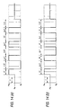
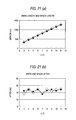
- Fig. 2 is a schematic diagram showing a power pattern of the recording light used in this recording method.
- a pattern shown in Fig. 2(b) is used.
- T is a reference clock period; and n is a mark length, an integer value, that can be taken in the mark length modulation recording
- the individual recording pulse widths are set to ⁇ i T (1 ⁇ i ⁇ m), each followed by the off pulse section of ⁇ i T (1 ⁇ i ⁇ m).
- the recording light with the recording power Pw is radiated and, in the ⁇ i T (1 ⁇ i ⁇ m) section, the bias power Pb (Pb ⁇ Pw) is radiated.
- the reference clock period T decreases as the density or speed increases. For example, T decreases in the following cases.
- a clock frequency needs to be increased to reduce the reference clock period T.
- the clock frequency is increased to reduce the reference clock period T.
- the reference clock period T during a x1-speed operation (linear velocity is 1.2-1.4 m/s) is 231 nanoseconds; but during a x10-speed operation the reference clock period T becomes very short, 23.1 nanoseconds.
- the reference clock frequency T during a x1-speed operation (3.5 m/s) is 38.2 nanoseconds, it is 19.1 ns during a x2-speed operation.
- the reference clock period T is very short.
- the recording pulse section ⁇ i T and the off pulse section ⁇ i T also tend to become short. Under these circumstances the following problems arise.
- the recording pulse section ⁇ i T may be too short for the rising/falling edge speed of radiated light, particularly a laser, to follow.
- a rise time is a time taken by the projected power of radiated light such as laser to reach a set value
- a fall time is a time taken by the projected power of the radiated light such as laser to fall from the set value to a complete off level.
- the rise and fall times take at least 2-3 nanoseconds respectively.
- the pulse width is less than 15 ns, for example, the time it takes for the light to actually project a required power is a few nanoseconds.
- the pulse width is less than five nanoseconds
- the projected power begins to fall before it reaches the set value, so that the temperature of the recording layer does not rise sufficiently, failing to produce a predetermined mark size.
- the recording medium cannot take a sufficient time to cool down and the off pulse function (cooling speed control function) does not work although the off pulse section is provided, leaving heat to be accumulated in the rear end part of the mark, making it impossible to form the correct shape of the mark. This problem becomes more serious as the length of the mark increases.
- phase change medium As an example.
- the currently available phase change medium typically takes crystal portions as an unrecorded state or erased state and amorphous portions as a recorded state.
- To form an amorphous mark involves radiating a laser onto a tiny area of the recording layer to melt that tiny portion and quickly cooling it to form an amorphous mark.
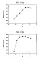
- a long mark (a mark more than about 5T in length based on the EFM modulation recording for CD format) is formed using a rectangular waveform of recording power with no off pulse section at all, as shown in Fig. 3(a)
- an amorphous mark with a narrow rear end is formed as shown in Fig. 3(b) and a distorted retrieve waveform is observed as shown in Fig. 3(c).
- Inserting the off pulse sections makes sharp the temperature change over time of the recording layer ranging from the front end to the rear end of the long mark, preventing degradation of the mark due to recrystallization during recording.
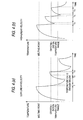
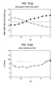
- Fig. 4 is a schematic temperature history of the mark starting end, with Fig. 4(a) representing a case in which the linear velocity is low and Fig. 4(b) a case in which the linear velocity is high. In either case, three temperature rising processes due to ⁇ 1 T, ⁇ 2 T, ⁇ 3 T and three cooling processes due to ⁇ 1 T, ⁇ 2 T, ⁇ 3 T are observed.
- the time during which the recording layer stays in the crystallization temperature range is much longer for T 4 +T 5 +T 6 of the high linear velocity than for T 1 +T 2 +T 3 of the low linear velocity, so it is understood that the recrystallization is more likely to take place at the fast linear velocity.
- a crystal is likely to grow at the amorphous/crystal boundary and therefore recrystallization easily occurs outer area of the mark.
- the phase change medium in which an amorphous mark is recorded over a crystal area, although it is generally easy at high linear velocity to secure an enough cooling speed to form an amorphous solid, the crystallization time is difficult to secure.
- the phase change medium often employs a recording layer of a composition which tends to be easily crystallized, i.e., a recording layer of an easily recrystallizable composition. Therefore, it is important to increase the off pulse section to enhance the cooling effect, but during the high linear velocity the off pulse section becomes short to the contrary.
- the similar problem is also encountered when the wavelength of a laser source is reduced or a numerical aperture is increased to reduce a beam diameter for enhancing the density of the phase change medium.
- the beam diameter is throttled to almost one-half.
- the energy distribution in the beam becomes steep so that the heated portion is easily cooled, allowing an amorphous mark to be formed easily. This however makes the recording layer more difficult to crystallize. In this case, too, it is necessary to increase the cooling effect.
- the present invention has been accomplished to solve the aforementioned problems. It is an object of the invention to provide an optical recording method and an optical recording medium suited for the method, which can perform recording in a satisfactory manner even during a mark length recording using a short clock period suited for high density recording and high speed recording.
- the inventors of this invention have found that the above objective can be realized by reducing the number of divisions m in the pulse division scheme from the conventional division number.
- the present invention provides an optical recording method for recording mark length-modulated information with a plurality of recording mark lengths by radiating light against a recording medium, the optical recording method comprising the steps of:
- the present invention provides a phase change type optical recording medium recorded by the optical recording method, the phase change type optical recording medium having a recording layer made of M z Ge y (Sb x Te 1-x ) 1-y-z alloy (where 0 ⁇ z ⁇ 0.1, 0 ⁇ y ⁇ 0.3, 0.8 ⁇ x; and M is at least one of In, Ga, Si, Sn, Pb, Pd, Pt, Zn, Au, Ag, Zr, Hf, V, Nb, Ta, Cr, Co, Mo, Mn, Bi, O, N and S).
- M is at least one of In, Ga, Si, Sn, Pb, Pd, Pt, Zn, Au, Ag, Zr, Hf, V, Nb, Ta, Cr, Co, Mo, Mn, Bi, O, N and S).
- the optical recording method of this invention reduces the number of divisions in the pulse division scheme, i.e., elongates each pulse of recording light to make the time during which to heat a light-irradiated portion of the optical recording medium sufficiently long with respect to the response speed of the laser pulse and also sets the time during which to cool the light-irradiated portion sufficiently long. This enables satisfactory mark length recording even with a clock period as low as 25 nm or less.
- time length of a recording mark is nT (T is a reference clock period equal to or less than 25 ns; and n is a natural number equal to or more than 2).
- ⁇ i T (1 ⁇ i ⁇ m) In the time length of ⁇ i T (1 ⁇ i ⁇ m), recording light with a recording power Pw i is radiated; and in the time length of ⁇ i T (1 ⁇ i ⁇ m), recording light with a bias power Pb i , which has the relation of Pb i ⁇ Pw i and Pb i ⁇ Pw i+1 , is radiated.
- the above pulse division number m is set to 2 or more; and as for the time length of all recording marks, n/m ⁇ 1.25.
- n-k division scheme sets the pulse division number m equal to n-k (k is 1 or 2)
- this invention defines the pulse division number m from a different perspective.
- the above pulse division number m is set to 2 or more. It should be noted, however, that there is no need to perform the pulse division for all nT marks (marks with a time length of nT; T is a reference clock period; and n is a natural number equal to or larger than 2).
- the problem of heat accumulation is relatively small but the response speed of the pulse being unable to follow the pulse division poses a more serious problem. It is therefore preferred that only one pulse of recording light with a recording power of Pw be radiated or that one pulse of recording light with the recording power of Pw and one pulse of recording light with a bias power of Pb be radiated.
- ⁇ 1 and ⁇ 2 are both 0.
- ⁇ i ( ⁇ i + ⁇ i )/m n/m
- the value of n/m corresponds to an average length of ( ⁇ i + ⁇ i )
- the value of (n/m)T corresponds to an average period of the divided pulse.
- n max T n max T
- n/m becomes minimum for n max . That is, because the average period of the divided pulses is longest for the shortest mark and shortest for the longest mark, ⁇ i T and ⁇ i T are shortest for the longest mark.
- n/m are approximately 1.22, 1.16 and 1.14.
- the average period of the divided pulses in the longest mark is generally less than 25 nanoseconds and the average value of the recording pulse section ⁇ i T or the average value of the off pulse section ⁇ i T is less than 12.5 nanoseconds. This means that for at least one i, either ⁇ i T or ⁇ i T is less than 12.5 nanoseconds. Further, when the clock period T goes below approximately 20 seconds, either ⁇ i T or ⁇ i T becomes further smaller.
- the average value of ⁇ i and ⁇ i becomes further smaller, making the problem more serious.
- m is set to satisfy the condition of n/m ⁇ 1.25 as to the time length of all recording marks ranging from short to long marks.
- the lengths of ⁇ i T and ⁇ i T are made sufficiently long.
- the recording pulse section ⁇ i T and the off pulse section ⁇ i T can generally be set slightly longer than 0.5T to sufficiently heat the recording layer and at the same time limit the heat being supplied from the subsequent pulses and thereby produce a sufficient cooling effect.
- n/m should preferably be set to 1.5 or more. It is of course preferred that, also for short marks 6T or shorter, n/m be set to 1.5 or more, more preferably to 1.8 or more.
- n/m is preferably set to 4 or less, more preferably 3 or less.
- the optical recording method of this invention produces a greater effect as the reference clock period T decreases, and it is preferred that the reference clock period be set to 20 nm or less or more preferably 15 ns or less.
- a very short clock period is difficult to achieve in practice and it is normally preferred that the clock period have 0.1 ns or more, or preferably 1 ns or more, or more preferably 3 ns or more.
- the clock period T decreases, it is desired that the minimum value of n/m be increased.
- the recording mark in this invention is recognized as a physical mark formed continuously in a recording medium and optically distinguishable from other portions. That is, the invention does not join, through processing by a reproducing system, 2T, 3T and 4T marks of the conventional n-k division scheme that meet the condition of n/m ⁇ 1.25 and recognize them as a single long mark.
- the recording mark may be formed of a plurality of physical marks that are below the optical resolution power of the retrieveing light. If we let the numerical aperture of an objective for focusing the retrieveing light be NA and the wavelength of the retrieveing light be ⁇ , when the physical marks are spaced from each other by 0.2 ( ⁇ /NA) or more, these physical marks can be optically distinguishable as separate marks.
- NA numerical aperture of an objective for focusing the retrieveing light
- ⁇ /NA the wavelength of the retrieveing light
- the parameters associated with the divided pulses such as ⁇ i , ⁇ i , ⁇ 1 , ⁇ 2 , Pw and Pb can be changed as required according to the mark length and i.
- the average value of the recording pulse section ⁇ i T (1 ⁇ i ⁇ m) and the average value of the off pulse section ⁇ i T (1 ⁇ i ⁇ m-1) both be set to 3 nanoseconds or more, preferably 5 nanoseconds or more, or more preferably 10 nanoseconds or more in terms of securing the response capability of the radiated light. More preferably, individual ⁇ i T (1 ⁇ i ⁇ m) and ⁇ i T (1 ⁇ i ⁇ m-1) are set to 3 nanoseconds or more, or 5 nanoseconds or more, or more specifically 10 nanoseconds or more.
- the rise time and fall time of the power of the laser beam normally used during the process of recording should preferably be set 50% or less of the minimum ⁇ i T (1 ⁇ i ⁇ m) and ⁇ i T (1 ⁇ i ⁇ m).
- ⁇ m T should preferably be provided. In that case, it is preferred that ⁇ m T be set normally to 3 nanoseconds or more, or specifically to 5 nanoseconds or more, or more preferably to 10 nanoseconds or more.
- the radiation energy required for recording can be secured by increasing the recording power Pw i although there is a problem of the rising/falling edge of the recording light.
- the cooling effect can be secured by reducing the bias power Pb down to nearly the retrieveing light power Pr or to 0 as long as this is not detrimental to a tracking servo or others.
- the values of ⁇ i (1 ⁇ i ⁇ m) and ⁇ i (1 ⁇ i ⁇ m-1) are set appropriately according to the values of the recording pulse section ⁇ i T (1 ⁇ i ⁇ m) and the off pulse section ⁇ i T (1 ⁇ i ⁇ m-1) and are normally set to 0.01 or more, preferably 0.05 or more, and normally 5 or less, preferably 3 or less. Too small a value of ⁇ i (1 ⁇ i ⁇ m-1) may result in an insufficient cooling effect and hence it is preferably set to 0.5 or more, specifically 1 or more. On the other hand, too large a value of ⁇ i may cause an excessive cooling and result in the recording mark being optically separated. Hence it is preferably set to 2.5 or less, specifically 2 or less. The effect of this setting is particularly large in the first off pulse section ⁇ i T that has a great effect on the shape of the front end of the mark.
- ⁇ m is normally set to 0.1 or more, preferably 0.5 or more, more preferably 1 or more, and 2.5 or less, preferably 2 or less.
- the switching period of intermediate pulse sections (group) ⁇ i T (2 ⁇ i ⁇ m-1) between the start pulse section ⁇ 1 T and the last pulse section ⁇ m T should preferably be set constant in terms of simplifying the circuit.
- ( ⁇ i + ⁇ i )T (2 ⁇ i ⁇ m-1) or ( ⁇ i + ⁇ i-1 )T (2 ⁇ i ⁇ m-1) is preferably set to 1.5T, 2T or 2.5T.
- the recording light power Pb i radiated during the off pulse section ⁇ i T (1 ⁇ i ⁇ m-1) is set smaller than the powers Pw i and Pw i+1 of the recording light radiated during the recording pulse sections ⁇ i T and ⁇ i+1 T.
- Pb i ⁇ Pw i be set for the time lengths of all recording marks. More preferably Pb i /Pw. ⁇ 0.5 and still more preferably Pb i /Pw i ⁇ 0.2.
- the bias power Pb can be set equal to the power Pr of the light radiated during retrieving. This simplifies the setting of the divided pulse circuit required for the pulse division.
- two or more different values of Pb i and/or Pw i may be used according to i.
- setting the recording powers Pw i and Pw m used in the start recording pulse section ⁇ 1 T and the last recording pulse section ⁇ m T to values different from the recording power Pw i used in the intermediate recording pulse sections ⁇ i T (2 ⁇ i ⁇ m-1) can control the shape of the front and rear ends of the mark accurately.
- the recording powers Pw i in the intermediate recording pulse sections ⁇ i T (2 ⁇ i ⁇ m-1) be set equal as practically as possible as this simplifies the setting of the divided pulse circuit.
- the bias powers Pb i in the off pulse sections ⁇ i T (1 ⁇ i ⁇ m-1) be all set to the same value as practically as possible unless there is any justifiable reason. At least two recording marks with different n's may have different values of Pw i and/or Pb i for the same i.
- the light to be radiated should preferably have a power Pe, which is Pb i ⁇ Pe ⁇ Pw i .
- the power Pe is an erase power used to erase the recorded marks.
- the recording power Pw and bias power Pb or erase power Pe have different physical functions depending on the type of the optical recording medium used.
- Pw or Pe is a power necessary to raise the temperature of the recording layer at least above the vicinity of the Curie temperature to make the occurrence of the magnetization inversion easy.
- Pw is greater than Pe and is a power to raise the temperatures of a plurality of magnetic layers with different Curie points above one of the Curie point temperatures.
- Pw is a power to raise the recording layer to a temperature higher than the crystallization temperature.
- Pw is a power to raise the recording layer at least to a temperature higher than its melting point.
- Pe is a power to raise the recording layer at least above the crystallization temperature.
- Pw is a power necessary to raise the recording layer to a temperature that induces softening, melting, evaporation, decomposition or chemical reaction.
- the recording power Pw and bias power Pb differ from one kind of recording medium used to another, in the rewritable phase change medium for example the recording power Pw is normally about 1-100 mW and the bias power Pb about 0.01-10 mW.
- the recording power Pw is a laser beam power necessary to raise the recording layer to a temperature that induces some optical changes in the recording layer, or to hold that temperature.
- the bias power Pb on the other hand is a power at least lower than the recording power Pw. Normally, the bias power Pb is lower than the recording power Pw and the erase power Pe and does not induce any physical changes in the recording layer.
- the heat accumulation problem described above is common to a wide range of optical disks that perform the mark length modulation recording, such as phase change type, magnetooptical type and write-once type optical recording media.
- the mark recording and mark erasing are performed at the same time by precisely controlling two temperature parameters, the heating speed and cooling speed of the recording layer, the function of cooling the recording layer by the off pulses bears more importance than in other write-once medium and magnetooptical medium.
- this invention is particularly effective for the phase change type recording medium.
- the same pulse division number m may be used on at least two recording marks which have different n's of time lengths nT of the pulse recording marks.
- the same m values are used for the nT marks having adjoining time lengths, such as 3T mark and 4T mark.
- m values set equal at least one of ⁇ i (1 ⁇ i ⁇ m), ⁇ i (1 ⁇ i ⁇ m), ⁇ 1 , ⁇ 2 , Pw i (1 ⁇ i ⁇ m) and Pb i (1 ⁇ i ⁇ m) is made to differ from others. This makes it possible to differentiate the time lengths of the marks from one another that have the same division numbers.
- the division numbers m may be arranged irrelevant to the magnitudes of the n values but it is preferred that the division numbers m be set to monotonously increase as the mark becomes longer, i.e., the value of m increases (including the case of staying the same).
- the pulse period ⁇ i is preferably synchronized to the reference clock period T or to the reference clock period T divided by an integer (preferably 1/2T, 1/4T, 1/5T, 1/10T) as this allows the rising/falling edge of the pulse to be controlled with one base clock taken as a reference.
- ⁇ i ( ⁇ i ) ⁇ i ( ⁇ i + ⁇ i ) does not necessarily agree with n and an excess time is produced, so that the pulse length must be corrected. It is preferred that the sum of the pulse irradiation times be set smaller than n because setting the sum greater than n makes the mark length too long.
- ⁇ 1 T, ⁇ 2 T light with the bias power Pb may be radiated. At this time, it is preferred that 0 ⁇ ( ⁇ 1 + ⁇ 2 ) ⁇ 1.
- ⁇ 1 and ⁇ 2 can also be used to correct the effect of heat transferred from other preceding and/or subsequent marks.
- the time lengths of ⁇ 1 T and ⁇ 2 T are made variable according to the mark lengths and/or space lengths of the preceding and/or subsequent marks.
- the divided pulse period ⁇ i and the duty ratio ( ⁇ i /( ⁇ i + ⁇ i )) are made variable according to i.
- the first recording pulse period ⁇ 1 and/or the last recording pulse period ⁇ m are made to differ from a recording pulse period ⁇ i (2 ⁇ i ⁇ m-1) of intermediate pulses.
- the first recording pulse section ⁇ 1 T be set larger than any of the subsequent recording pulse sections ⁇ 2 T, ..., ⁇ m T. It is also preferred that the recording power Pw 1 be set higher than the recording power Pw i in the succeeding recording pulse sections ⁇ 2 T, ..., ⁇ m T. These methods are effective in improving an asymmetry value of the retrieve signal described later.
- the heat accumulation effect is small in short marks such as those with time lengths of 3T and 4T, so that the mark tends to be formed slightly shorter than required.
- the mark time length may be strictly controlled by elongating the recording pulse section ⁇ 1 T to some extent or setting the recording power Pw 1 in the recording pulse section ⁇ 1 T slightly higher than required.
- the method of changing the first pulse or last pulse is particularly effective when overwriting an amorphous mark in the crystal area of the phase change medium.
- Changing the first recording pulse section ⁇ 1 T can control the width of an area of the recording layer in the phase change medium that first melts.
- the last off pulse section ⁇ m T is important in preventing the recording layer of the phase change medium from getting recrystallized and is also an important pulse that determines the area in which the recording layer is made amorphous.
- the degree of modulation can be controlled without affecting the mark edges.
- the above pulse division can basically be realized by making the division scheme for each mark time length nT programmable and incorporating it into a ROM chip.
- adding a very wide range of flexibility to the same pulse generating circuit will render the circuit complex. So, the following two pulse generating methods may preferably be used. They can provide pulses capable of dealing with almost all media with ease.
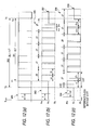
- the circuits Gate1, Gate 2, Gate3, Gate4 that generate clocks at timings shown in Fig. 1(c) are combined to realize the division scheme of Fig. 1(b).
- the Gate1 denoted 102 generates the first recording pulse ⁇ 1 T with a delay time of T d1 .
- the Gate2 denoted 103 generates a group of second and subsequent intermediate recording pulses ⁇ i T with a delay time of T d2 .
- the Gate3 denoted 104 generates pulses with a bias power Pb and pulses with power Pe. That is, when recording pulses are not generated by the Gate1, Gate2 and Gate4, off pulses ⁇ i T with a bias power Pb aretrieved when the level is low and pulses with a power Pe aretrieved when the level is high.
- the Gate3 and T d1 determine (n - ( ⁇ 1 + ⁇ 2 ))T.
- the Gate4 denoted 105 generates a last recording pulse ⁇ m T with a delay time of T d3 after the intermediate recording pulse group ⁇ i T has been generated.
- the Gate3 is at low level, when the recording pulses are at high level, they have priority over the off pulses.
- ⁇ 1 T can be controlled independently by the delay time T d2 and ⁇ 1 T, and ⁇ m T can be controlled independently by Gate3 and ⁇ m T.
- a recording power Pw 1 is used; in the sections where the intermediate pulse group ⁇ i T is generated by the Gate2, a recording power Pw 2 is used; and in the section where the ⁇ m T pulse is generated by the Gate4, a recording power Pw 3 is used.
- This arrangement allows the recording power to be controlled independently in each of the first pulse section, the intermediate pulse section group and the last pulse section.
- the Gate timing is synchronized with the reference clock period T or with a base clock, which is the reference clock period divided by an integer, and that ⁇ i and ⁇ i are defined by the duty ratio with respect to the base clock.
- the intermediate pulses are generated, according to n, in numbers equal to the division number stored in the ROM memory.
- the last pulse ⁇ m T generated by the Gate4 is generated only when n ⁇ n c + 1. This is indicated by a 9T mark in Fig. 1.
- n n c
- the pulse is divided into two pulses, the first pulse and one intermediate pulse. In Fig. 1 this is represented by a 5T mark.
- the following description concerns a divided recording pulse generating method based on a clock signal with a period of 2T which is obtained by dividing the reference clock period T.
- This method has more limitations than the divided recording pulse generating method 1 but has an advantage of allowing for the design of logic circuits based on more regular rules.
- the pulse generating method 2 is characterized in that the procedure depends on whether the value that n of an nT mark can take is odd or even.
- ⁇ 1 , ⁇ 1 , ⁇ 1 ', ⁇ 1 ', ⁇ 1 , ⁇ 2 , ⁇ 1 ', and ⁇ 2 ' may change according to the value of L.
- the ⁇ is normally 1 but can be changed in a range of about 0.8 to 1.2, considering the influence of heat interference from the preceding and subsequent recording marks.
- ⁇ 1 and ⁇ 2 , and ⁇ 1 ,' and ⁇ 2 ' are adjusted to ensure that each mark length will be precisely nT and to reduce jitters at the ends of the mark. They are normally -0.5 ⁇ 1 ⁇ 0.5, -0.5 ⁇ 1 ' ⁇ 0.5, -1 ⁇ 2 ⁇ 1 and -1 ⁇ 2 ' ⁇ 1.
- the correction amounts at the front end and rear end are preferably set equal, i.e.,
- are each preferably in the range of 0.8 to 1.2.
- the position of the front end of the mark is determined almost by the rising edge of the recording power laser beam at ⁇ 1 T and its jitter is determined by the duty ratio of ⁇ 1 and ⁇ 1 , and by the duty ratio of ⁇ 1 ' and ⁇ 1 '.
- the mark rear end position depends on ⁇ 2 (and ⁇ 2 '), i.e., the value of the divided pulse period ( ⁇ m + ⁇ m )T (and ( ⁇ m ' + ⁇ m ')T) at the rear end of the mark and also on the value of the duty ratio of ⁇ m and ⁇ m (and the duty ratio of ⁇ m ' and ⁇ m ') Further, the mark rear end position also depends on the position of the falling edge of the recording pulse ⁇ m T (and ⁇ m 'T) at the rear end and on the cooling process of the recording layer before and after that falling edge position.
- the mark rear end position depends on the value of the off pulse section ⁇ m T (and ⁇ m 'T) at the rear end that has a great effect on the cooling speed of the recording layer.
- the divided pulse period ( ⁇ m + ⁇ m )T at the rear end does not need to be 0.5T or 1T, and fine adjustment can be made with a resolution power of about 0.1T, preferably 0.05T, or more preferably 0.025T.
- ⁇ 1 and ⁇ 1 assume fixed values for all L equal to 3 or more.
- ⁇ 1 + ⁇ 1 be set to 2 as this causes the period ( ⁇ i + ⁇ i )T to become 2T for all i ranging from 1 to (m - 1).
- ⁇ 1 ' and ⁇ 1 ' assume fixed values for all L equal to 3 or more.
- ⁇ 1 + ⁇ 1 be set to 2.5 as this makes it easy to synchronize with the subsequent divided pulse period 2T.
- ⁇ m , ⁇ m , ⁇ m ' and ⁇ m ' each preferably assume the same values for all L equal to 3 or more, specifically 2 or more.
- the circuit can be further simplified.
- the division number m is 1.
- the ⁇ 1 - ⁇ 1 duty ratio and ⁇ 1 (or the ⁇ 1 '- ⁇ 1 'duty ratio and ⁇ 1 ') can be adjusted to achieve a desired mark length and jitter.
- it is desired that ⁇ 1 '- ⁇ 1 1.
- the pulse generating circuit should preferably be controlled to ensure that ⁇ i (1 ⁇ i ⁇ m) is generated in synchronism with a frequency-divided first reference clock 3 with a period 2T which is produced by frequency-dividing a first reference clock 1 with a period T; that ⁇ i ' (2 ⁇ i ⁇ m) is generated in synchronism with a frequency-divided second reference clock 4 with a period 2T which is obtained by frequency-dividing a second reference clock 2 that has the same period T as that of the first reference clock 1 and is shifted 0.5T from the first reference clock 1; and that ⁇ 1 ' rises 2.5T before ⁇ 2 ' rises.
- the use of a plurality of reference clocks can simplify the pulse generating circuit.
- T d1 is a real number between -2 and 2. When the value of Td 1 is negative, it indicates a advance time.
- Fig. 12 shows an example relation between recording pulses when the pulse division scheme in the recording method of this invention is implemented by using a plurality of reference clocks described above.
- the delay times T d1 of ⁇ 1 T and ⁇ 1 'T with respect to the front end of the nT mark are 0;
- the recording power in the recording pulse section ⁇ i 'T (1 ⁇ i ⁇ m) is Pw which is constant;
- the bias power in the off pulse section ⁇ i T (1 ⁇ i ⁇ m) is Pb which is constant;
- the power of light radiated in the spaces and in other than ⁇ i T (1 ⁇ i ⁇ m) and ⁇ i T (1 ⁇ i ⁇ m) is an erase power Pe which is constant.
- reference number 200 denotes a reference clock with a period T.
- Fig. 12(a) shows a pulse waveform corresponding to a recording mark with a length of nT, with reference number 201 representing the length of a 2LT recording mark and 202 representing the length of a (2L + 1)T recording mark.
- a frequency-divided second reference clock 206 with a period 2T is obtained by frequency-dividing a second reference clock 204 with a period T which has a phase shift of 0.5T from the reference clock 200.
- the duty ratio of ⁇ i - ⁇ i is adjusted to produce a recording pulse waveform 208.
- Fig. 13 is a timing chart explaining the above gate generating method.
- the reference number 300 represents the reference clock with a period T (reference clock for data).
- the recording system normally makes a phase comparison between the synchronization signal T sync generated at clock marks arranged on the medium for each minimum unit of address (e.g., synchronization signal such as VFO formed as a pit train on the medium and arranged for each sector, and a synchronization pattern arranged for each ATIP frame (every 1/75 second) formed as a groove meander on the medium) and the T-period reference clock generated in advance in order to establish synchronization.
- T sync generated at clock marks arranged on the medium for each minimum unit of address
- synchronization signal such as VFO formed as a pit train on the medium and arranged for each sector
- a synchronization pattern arranged for each ATIP frame (every 1/75 second) formed as a groove meander on the medium)
- the T-period reference clock generated in advance in order to establish synchronization.
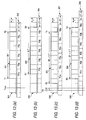
- Fig. 13 shows an example case in which the front end of the mark appears an even number of periods T after the T sync .
- An even-numbered length mark 301 with n being even is shown in Fig. 13(a) and an odd-numbered length mark 304 with n being odd is shown in Fig. 13(d).
- an even-numbered length mark 302 with n being even is shown in Fig. 13(b)
- an odd-numbered length mark 303 with n being odd Fig. 13(c)
- Fig. 13(a) to 13(d) when reference clocks are generated by shifting them 0.5T from one another in a manner similar to that of Fig. 12, four different clock trains are produced, as indicated by 305, 306, 307 and 308. That is, with the reference clock 305 taken as a reference, the clock 307 is shifted by 0.5T, the clock 306 is shifted by 1T, and the clock 308 is shifted by 1.5T. These clocks are all formed by frequency-dividing the T-period reference clock having its origin at T sync and then shifting their phases by 0.5T from one another.
- the recording pulse generating gate groups G1a, G1b, G2a and G2b are identical to the Gate1, Gate2 and Gate4 combined in Fig. 1. That is, in Fig. 1, the Gate1 for generating the first pulse ⁇ 1 T, the Gate2 for generating the intermediate pulse group ⁇ i T (2 ⁇ i ⁇ m-1), and the Gate4 for generating the last pulse ⁇ m T are produced separately and then combined to generate the gate groups G1a and G1b. In Fig. 1, the first pulse ⁇ 1 'T, the intermediate pulse group ⁇ i 'T (2 ⁇ i ⁇ m-1), and the last pulse ⁇ m 'T are produced separately and then combined to generate the gate groups G2a and G2b.
- Generating the first pulse independently as with the Gate1 of Fig. 1 can deal with the situation where ( ⁇ 1 ' + ⁇ 1 ') is 2.5 when n is odd, by generating the gate for ⁇ 1 'T in synchronism with the front end of nT and generating the 2T-period intermediate pulse group ⁇ i 'T with a delay of 2.5T. This is equivalent to setting the T d2 for Gate2 in Fig. 1 to 2.5T (when there is a delay T d1 , another delay T d1 is made).
- the gate groups G1a, G1b, G2a and G2b are selected as follows. First, with T sync taken a reference, the starting point of the T-period reference clock 300 is determined, and it is checked whether the mark length nT rises an even number of clock periods T or an odd number of clock periods T after the starting point. More specifically, a 1-bit adder is used which is reset at T sync and adds 1 every period. If the result is 0, it is decided that the elapsed time is determined to be an even number of periods; and if the result is 1, the elapsed time is determined to be an odd number of periods.
- the gate signal group G1a or G2b is selected depending on whether n is even or odd. If the elapsed time from the reference time Tsync to the front end of the nT mark is an odd number times the period T, then the gate signal group G1b or G2a is selected depending on whether n is even or odd. It is therefore possible to generate all the recording pulses in a series of nT marks which are generated, with T 0 as a starting point, by using combinations of the four 2T-period reference clocks shifted 0.5T from one another.
- the gate signals are generated depending on whether n is even or odd, that is, a gate G3 of ⁇ ( ⁇ i + ⁇ i ) is generated with a delay time of T d1 when n is even; and a gate G4 of ⁇ ( ⁇ i ' + ⁇ i ') is generated with a delay time of T d1 when n is odd, to radiate light with different powers according to the following conditions.
- the gate priority relationship described above is determined by matching the gate on/off to logical 0 and 1 levels and performing an OR operation on each gate controlling logical signal.
- Fig. 12 and Fig. 13 represent a case where, for simplicity, the rising edge of the first recording pulse ⁇ 1 T, ⁇ 1 'T is at the front end of the nT mark, i.e., concurrent with the front end of the nT mark being recorded. If the mark has a delay, it is preferred in terms of keeping the space length at a desired value that the rising edges of ⁇ 1 T and ⁇ 1 'T be provided with the same delay T d1 .
- the following description concerns another example of the divided recording pulse generating method based on a 2T-period clock signal which is obtained by dividing the reference clock period T.
- This method allows for the design of logic circuits based on more regular rules than those employed in the divided recording pulse generating method 1.
- the procedure depends on whether the value the n of an nT mark can take is odd or even.
- the correction of the mark length difference 1T between an even-numbered length mark and an odd-numbered length mark, both having the same number of divisions, is distributed and allocated to the first and last recording pulse periods.
- the correction of the mark length difference 1T is done by adjusting the off pulse length ⁇ i T (2 ⁇ i ⁇ m-1) in the intermediate divided recording pulse group.
- ⁇ 1 , ⁇ 2 , ⁇ m-1 , ⁇ m , ⁇ 1 ', ⁇ 2 ', ⁇ m-1 and ⁇ m ' satisfy the following equation.
- ⁇ i , ⁇ i , ⁇ i ', ⁇ i ', T d1 , T d1 ', ⁇ 1 , ⁇ 1 ', ⁇ 2 ' and ⁇ 3 ' can vary according to L.
- T d1 and T d1 ' are delay or advance times from the starting end of the nT mark in the mark length-modulated original signal until the first recording pulse ⁇ 1 T rises. They are real numbers normally between -2 and 2.
- the positive values of T d1 and T d1 ' signify delays.
- Td 1 and T d1 ' are preferably set almost constant regardless of the value of L.
- ⁇ i , ⁇ i , ⁇ i ' and ⁇ i ' are real numbers normally between 0 and 2, preferably between 0.5 and 1.5.
- ⁇ 1 , ⁇ 1 ', ⁇ 2 ' and ⁇ 3 ' are real numbers normally between -1 and 1, preferably between -0.5 and 0.5. These are used, as required, as correction values for realizing precise mark lengths or space lengths in the divided pulse periods ( ⁇ i-1 + ⁇ i )T that form the period 2T.
- the period ( ⁇ 1 + ⁇ 2 )T and the period ( ⁇ m-1 + ⁇ m )T are each increased or decreased by 0.5T to adjust their lengths.
- What is important in the mark length recording is the mark end position and the jitter that are determined by the waveform of the front and rear ends of the mark.
- the intermediate portion of the mark does not have a great effect on the jitter at the ends of the mark as long as the correct amplitude of the intermediate portion is obtained.
- the above adjusting method takes advantage of the fact that as long as the mark does not appear optically divided, if the recording pulse period in the intermediate portion of the mark is extended or reduced by 0.5T, the mark length only increases or decreases by the corresponding amount and does not greatly affect the jitter at the ends of the mark.
- 2T is taken as the base recording pulse period for any mark length.
- the duty ratio of ⁇ i - ⁇ i can be optimized for each mark length or for each i, but it is preferred that the following restrictions be provided for the simplification of the recording pulse generating circuit.
- the rear end position of the mark depends not only on the trailing edge position of the last recording pulse ⁇ m T (or ⁇ m 'T) but also on the cooling process of the recording layer temperature before and after the mark rear end position.
- the values of T d1 , ⁇ 1 , ⁇ 1 ', ⁇ 1 , ⁇ 1 ', ⁇ m , ⁇ m ', ⁇ m and ⁇ m ' can be finely adjusted in the range of about ⁇ 20% to correct the heat interference according to marks or spaces immediately before or after the mark being recorded.
- the expression "about 0.5" or "about 1" means that the fine adjustment of that degree is allowed.
- L 3 or more
- the expression "L is 3 or more" is the condition to establish that the division number is 3 or more and there is one or more intermediate divided recording pulses excluding first and last divided pulses.
- ⁇ m and ⁇ m ' be set to the same values of ⁇ i and ⁇ i ' for 2 ⁇ i ⁇ m-1.
- an original mark length modulation signal is generated in synchronism with the first reference clock with a period T.
- the first recording pulse ⁇ 1 T (or ⁇ 1 'T) is generated with a delay time of T d1 (or T d1 ').
- the last recording pulse ⁇ m T ( ⁇ m 'T) is generated so that its falling edge aligns, after a time difference of ⁇ 3 (or ⁇ 3 '), with the rear end of the nT mark.
- the falling edge of at least ⁇ 2 T or ⁇ 2 'T in the intermediate divided recording pulse group is produced precisely the delay time of 4T or 4.5T after the starting end of the nT mark. Therefore, at least the intermediate divided recording pulse group can be generated in synchronism with the 2T-period reference clock, which was generated by frequency-dividing the T-period reference data clock in advance.
- Fig. 24 shows the relation between the recording pulses when the recording pulse dividing method of this invention is implemented by combining a plurality of 2T-period reference clocks.
- the recording power Pw of light radiated during the recording pulse sections, the bias power Pb of light radiated during the off pulse sections, and the erase power Pe of light radiated during other than these sections are each shown to be constant for any i.
- these powers are shown to have the relationship of Pb ⁇ Pe ⁇ Pw, these powers may be set to different values depending on the values of n and i.
- reference number 220 represents a T-period reference clock.
- Fig. 24(a) shows square waves associated with the nT mark of the original mark length modulation signal, with 221 representing a mark 2LT in length and 222 representing a mark (2L + 1)T in length.
- L 5
- the 2T-period reference clock 225 is obtained by frequency-dividing a T-period reference clock 223 which has no phase delay with respect to the T-period reference clock 220.
- T d1 + ⁇ 1 2
- the falling edge of each recording pulse ⁇ i T (1 ⁇ i ⁇ m) is synchronized with the 2T-period reference clock 225.
- the duty ratio of ⁇ i - ⁇ i is adjusted to produce a recording pulse waveform 227.
- a 2T-period reference clock 226 is obtained by frequency-dividing a T-period reference clock 224 which is 0.5T out of phase with the T-period reference clock 220.
- the falling edge of each recording pulse ⁇ i 'T (2 ⁇ i ⁇ m) is synchronized with the 2T-period reference clock 226.
- the duty ratio of ⁇ i-1 - ⁇ i is adjusted to produce a recording pulse waveform 228.
- the mark lengths 2LT and (2L + 1)T are depicted to have their rear ends align with each other at T2 and T4. So, there are only two possible relations (b) and (c) between the 2T-period reference clocks 225 and 226. In reality, however, when the 2T period reference clocks are used, the front end positions of these mark lengths can be 1T out of phase with each other although they are in phase with the 2T period.
- the divided recording pulse generating method 3 needs also to consider, as in the divided recording pulse generating method 2, the fact that there are four possible relations considering the cases of n being even and n being odd as shown in Fig. 13(a), (b), (c) and (d).
- a gate group G1a corresponding to the recording pulse sections ⁇ 1 T, ⁇ 2 T, ⁇ 3 T, ⁇ 4 T, ⁇ 5 T is generated in synchronism with each of the periods P1a, P2a, P3a, P4a, P5a;
- a gate group G1b corresponding to the recording pulses ⁇ 1 T, ⁇ 2 T, ⁇ 3 T, ⁇ 4 T, ⁇ 5 T is generated in synchronism with each of the periods P1b, P2b, P3b, P4b, P5b;
- a gate group G2a corresponding to the recording pulses ⁇ 1 'T, ⁇ 2 'T, ⁇ 3 'T, ⁇ 4 'T, ⁇ 5 'T is generated in synchronism with each of the periods R1a, R2a, R3a, R4
- These recording pulse generating gate groups G1a, G1b, G2a, G2b are identical to the combinations of Gate 1,2, and 4 in Fig. 1, as in the case of the divided recording pulse generating method 2.
- the Gate1 for generating the first pulse ⁇ 1 T, the Gate2 for generating the intermediate pulse group ⁇ i T (2 ⁇ i ⁇ m-1), and the Gate4 for generating the last pulse ⁇ m T are separately generated and then combined.
- the first pulse ⁇ 1 'T, the intermediate pulse group ⁇ i 'T (2 ⁇ i ⁇ m-1), and the last pulse ⁇ m 'T are separately produced and then combined.
- the first recording pulses ⁇ 1 T, ⁇ 1 'T may be given a predetermined time difference of period P1a, Q1a, P1b or Q1b, and the last recording pulses ⁇ m T, ⁇ m 'T are given a predetermined time difference of either period P5a, P5b, Q5a or Q5b.
- the last off pulse section ⁇ m T of the mark is irregular. That is, the period of the rear end of the mark is not necessarily 2T and must be given a margin of about 2T ⁇ 1T. This can be dealt with by defining the last off pulse ⁇ m or ⁇ m ' exceptionally. For that purpose, the gate signal corresponding to the Gate3 of Fig. 1 is generated.
- a gate G3 of ⁇ ( ⁇ i + ⁇ i )T is generated with a delay time T d1 from the front end of the nt mark; and when n is odd, a gate G4 of ⁇ ( ⁇ i ' + ⁇ i ')T is generated with a delay time T d1 ' from the front end of the nT mark.
- the light with the erase power Pe is radiated; when either G3 or G4 is on, the light with the bias power Pb is radiated; when both G3 and G1a are on simultaneously, the light with the recording power Pw is radiated in response to the G1a-on section; when both G3 and G1b are on simultaneously, the light with the recording power Pw is radiated in response to the G1b-on section; when both G4 and G2a are on simultaneously, the light with the recording power Pw is radiated in response to the G2a-on section; and when both G4 and G2b are on simultaneously, the light with the recording power Pw is radiated in response to the G2b-on section.
- the gate priority relationship described above is determined by matching the gate on/off to logical 0 and 1 levels and performing an OR operation on each gate controlling logical signal.
- all the gates for generating the recording pulse sections ⁇ i T can be produced by the following procedure.
- a reference time T sync corresponding to the clock mark formed at a predetermined position on the recording track is generated;
- four reference clocks are generated: a 2T-period reference clock 1a produced at the reference time T sync as a starting point, a 2T-period reference clock 2a produced 0.5T in advance of the reference clock 1a, 2T-period reference clock 1b produced 1T in advance of the reference clock 1a, and a 2T-period reference clock 2b produced 1.5T in advance of the reference clock 1a;
- (4) in recording a mark of nT (2L + 1)T, the
- the gate groups G1a, G1b, G2a, G2b can be selected as follows. First, it is checked whether the mark length nT rises an even number of clock periods T or an odd number of clock periods T after the reference time T Sync as a start point. More specifically, a 1-bit adder is used which is reset at T sync and adds 1 every period. If the result is 0, it is decided that the elapsed time is determined to be an even number of periods; and if the result is 1, the elapsed time is determined to be an odd number of periods.
- the gate signal group G1a or G2b is selected depending on whether n is even or odd. If the elapsed time from the reference time T sync to the front end of the nT mark is an odd number times the period T, then the gate signal group G1b or G2a is selected depending on whether n is even or odd. It is therefore possible to generate all the recording pulses in a series of nT marks which are generated, with T 0 as a starting point, by using combinations of the four 2T-period reference clocks shifted 0.5T from one another.
- the optical recording method of this invention is particularly effective for a phase change medium in which information is overwritten by forming an amorphous mark on a crystal-state medium, the crystal state being taken as an unrecorded or erased state.
- the optical recording method of this invention is also effective in cases where the recording is made on the same medium at different linear velocities.
- a constant density recording is commonly practiced, which does not depend on the linear velocity but keeps a product of vT at a plurality of linear velocities constant, where v is a linear velocity and T is a clock period.
- the pulse generation method 2 keeps the periods of ( ⁇ i + ⁇ i )T and ( ⁇ i ' + ⁇ i ')T for 2 ⁇ i ⁇ m-1 constant irrespective of the linear velocity, also keeps Pw i , Pb i and Pe for each i almost constant irrespective of the linear velocity, and reduces ⁇ i and ⁇ i ' (1 ⁇ i ⁇ m) as the linear velocity becomes slower (JP-A 9-7176). As a result, a satisfactory overwrite is made possible in a wide range of linear velocity.
- the pulse generation method 3 keeps the periods of ( ⁇ i-1 + ⁇ i )T and ( ⁇ i-1 ' + ⁇ i ')T for 2 ⁇ i ⁇ m constant irrespective of the linear velocity, also keeps Pw i , Pb i and Pe for each i almost constant irrespective of the linear velocity, and monotonously reduces ⁇ i and ⁇ i ' as the linear velocity becomes slower (JP-A 9-7176). In this case, too, a satisfactory overwrite is made possible in a wide range of linear velocity.
- the method of reducing ⁇ i and increasing ⁇ i in ( ⁇ i + ⁇ i )T and reducing ⁇ i and increasing ⁇ i-1 in ( ⁇ i + ⁇ i )T as the linear velocity decreases is particularly effective in the phase change medium. This is because in the phase change medium, the cooling speed of the recording layer becomes slower as the linear velocity decreases and it is necessary to accelerate the cooling effect by increasing the ratio of the off pulse section ⁇ i .
- ⁇ i and ⁇ i ' be set to 0.5 ⁇ ⁇ i ⁇ 2.5 and 0.5 ⁇ ⁇ i' ⁇ 2.5, more preferably 1 ⁇ ⁇ i ⁇ 2 and 1 ⁇ ⁇ i ' ⁇ 2, to secure the cooling time to change the medium into the amorphous state.
- ⁇ i T and ⁇ i 'T (2 ⁇ i ⁇ m-1) be held constant, i.e., the intermediate recording pulses have almost constant absolute lengths of time.
- the expression "almost constant” means that they have a variation range of about ⁇ 0.1T at each linear velocity. In that case, the reference clock T becomes large as the linear velocity decreases, so ⁇ i and ⁇ i ' in the intermediate pulse group necessarily decrease monotonously.
- the first recording pulse sections ⁇ 1 T, ⁇ 1 'T can be made constant, they should preferably be finely adjusted at each linear velocity.
- the ⁇ m and ⁇ m ' are preferably fine-adjusted at each linear velocity. In that case, it is preferred that ⁇ m and ⁇ m ' be set constant or made to increase as the linear velocity decreases.
- n - ( ⁇ 1 + ⁇ 2 ) and the first and last pulses should preferably be controlled according to the preceding and/or subsequent mark lengths or space lengths.
- a first case is where the linear velocity during the recording is set as high as 10 m/s or more and the shortest mark length as small as 0.8 ⁇ m or less in order to perform high density recording. Because the shortest mark length is expressed as nT x V where V is the linear velocity, the reduced shortest mark length results in the reference clock period T being shortened.
- the wavelength of the recording light is also effective to set the wavelength of the recording light to as short as 500 nm or less, the numerical aperture of the lens for focusing the recording light to as high as 0.6 or more, the beam diameter of the recording light to a small value, and the shortest mark length to as small as 0.3 ⁇ m or less to perform high density recording.
- high density recording modulation scheme such as a 8-16 modulation scheme and a (1, 7)-RLL-NRZI modulation scheme, as the mark length modulation scheme.
- mark length modulation scheme is an EFM modulation scheme and the linear velocity during recording is set to a very high speed of 10 times the CD reference linear velocity of 1.2 m/s to 1.4 m/s while keeping the recording line density constant during the recording.
- the mark length modulation scheme is an EFM+ modulation scheme
- the high density recording scheme and the linear velocity during recording is set to as high as two or more times the DVD reference linear velocity of 3.49 m/s while keeping the recording line density constant during the recording.
- Fig. 5 is a schematic diagram showing retrieved waveforms (eye-pattern) of the EFM modulation signal used in the CD family including Cd-RW.
- the recording mark and space lengths can take a time length of between 3T and 11T and the eye-pattern virtually randomly includes retrieved waveforms of all amorphous marks from 3T to 11T.
- the EFM+ modulation further includes a mark length of 14T and a space length of 14T.
- the upper end I top of the eye-pattern converted into the reflectance is an upper end value R top
- m 11 is preferably set between 40% and 80% and it is particularly important to set m 11 to 40% or more. It is preferred that the signal amplitude be set large, but too large a signal amplitude will result in the gain of the amplifier of the signal reproducing system becoming excessively saturated. So, the upper limit of m 11 is set at around 80%. Too small a signal amplitude on the other hand will reduce the signal-noise ratio (SN ratio) and thus the lower limit is set at around 40%.
- SN ratio signal-noise ratio
- asymmetry value Asym ( I slice I 11 - 1 2 )(%)
- the jitter of each mark and space of the retrieved signal be almost 10% or less of the reference clock period T and that the mark length and space length have nearly nT x V (T is a reference clock period of data, n is an integer from 3 to 11, and v is a linear velocity during reproduction).
- T is a reference clock period of data
- n is an integer from 3 to 11
- v is a linear velocity during reproduction.
- equations (1) and (2) are defined by replacing I 11 with an amplitude I 14 of a 14T mark.
- the jitter is measured as a so-called edge-to-clock jitter, which is obtained by passing an analog retrieved signal through an equalizer to digitize it.
- the value of jitter is preferably 13% or less of the clock period, particularly 9% or less.
- Optical recording mediums recorded according to this invention include a pigment-based organic recording medium, a magnetooptical recording medium, a phase change recording medium and various other types of recording mediums. They also include a write-once and rewritable mediums. Of these mediums, the one that can produce a particularly significant effect is the phase change recording medium, particularly a rewritable phase change recording medium in which an amorphous mark is overwritten on a crystal-state medium, the crystal state being taken as an unrecorded state.
- a particularly preferred material of the recording layer is of a type in which crystallization initiates at an interface between a crystal area and a melted area.
- phase change mediums are those having a recording layer containing still more excessive Sb in the SbTe eutectic composition.
- a particularly preferred composition is the one which contains excessive Sb and also Ge in the base Sb 70 Te 30 eutectic composition.
- the Sb/Te ratio is particularly preferably set to 4 or more.
- the content of Ge is preferably 10 atomic % or less.
- Such a recording layer is a M z Ge y (Sb x Te 1-x ) 1-y-z alloy (where 0 ⁇ z ⁇ 0.1, 0 ⁇ y ⁇ 0.3, 0.8 ⁇ x; and M is at least one of In, Ga, Si, Sn, Pb, Pd, Pt, Zn, Au, Ag, Zr, Hf, V, Nb, Ta, Cr, Co, Mo, Mn, Bi, O, N and S).
- the alloy with the above composition is a binary alloy containing excessive Sb at the Sb 70 Te 30 eutectic point and which contains Ge for for improving the time-dependent stability and jitter, and also contains at least one of the series of elements represented by M for further reduction of jitter and improvement of linear velocity dependency and optical characteristics.
- a composition with the Te amount close to zero can be regarded as an alloy that has Te or M element added in the composition near the Ge 15 Sb 85 eutectic point.
- Ge acts to enhance the time-dependent stability of the amorphous mark without degrading the high speed crystallization function offered by excess Sb. It is considered to have a capability to raise the crystallization temperature and enhance the activation energy for crystallization. That is, the above-mentioned alloy recording layer consisting mainly of GeSbTe in the base SbTe eutectic composition can increase the Sb/Te ratio while suppressing the formation of crystal nucleus by the presence of Ge and thereby increase the speed of crystal growth. Generally, the forming of crystal nucleus initiates at a lower temperature than that of the crystal growth and this is not desirable to the storage stability of the mark at around the room temperature when amorphous marks are formed.
- the alloy recording layer with the above GeSbTe as a main component because the crystal growth at near the melting point is selectively promoted, this alloy is capable of quick erasure and has an excellent stability of the amorphous mark at room temperature. In this sense, the alloy recording layer described above is particularly suited for high linear velocity recording.
- a more preferred composition of the recording layer of the phase change medium is A 1 a A 2 b Ge c (Sb d Te 1-d ) 1-a-b-c alloy (where 0 ⁇ a ⁇ 0.1 0 ⁇ b ⁇ 0.1, 0.02 ⁇ c ⁇ 0.3, 0.8 ⁇ d; A 1 is at least one of Zn, Pd, Pt, V, Nb, Ta, Cr, Co, Si, Sn, Pb, Bi, N, O and S; and A 2 is In and/or Ga).
- compositions are preferable because, compared with the composition near the conventional GeTe-Sb 2 Te 3 pseudo-binary alloy, the reflectance of individual fine crystal grains has a smaller dependency on the direction of crystal plane, providing these compositions with the ability to reduce noise.
- the SbTe-based composition with the above Sb/Te ratio higher than 80/20 is excellent in that it is capable of quick erasure at high linear velocities equal to or more than 12 times the CD linear velocity (about 14 m/s) or 4 times the DVD linear velocity (about 14 m/s).
- the erasure of the amorphous mark in the above composition is virtually governed only by the crystal growth from the boundary with the crystal area surrounding the amorphous mark, and the formation of a crystal nucleus inside the amorphous mark and the process of crystal growth from the crystal nucleus hardly contribute to the recrystallization process.
- the linear velocity increases (e.g., to more than 10 m/s)
- the time that the erase power Pe is irradiated becomes short, extremely reducing the time that the layer is kept at a high temperature around the melting point necessary for the crystal growth.
- the increased content of Sb also increases the crystal growth speed during the re-solidifying of the melted area. That is, increasing the Sb content to ensure the quick erasure of the amorphous mark during the high linear velocity recording makes the formation of good amorphous marks difficult.
- the speed of recrystallization from around the amorphous mark is increased above a certain level, the recrystallization from around the melted area during the re-solidifying of the melted area formed to record the amorphous mark is also accelerated.
- the composition problem described above is considered relatively not so large with the commonly used conventional GeTe-Sb 2 Te 3 pseudo-binary alloy-based composition.
- the erasure of the amorphous mark is effected mostly by the formation of crystal nuclei within the amorphous mark and not very much by the crystal growth. Further, the formation of crystal nuclei is more active than the crystal growth at low temperatures.
- the recrystallization can be achieved by generating a large number of crystal nuclei even when the crystal growth is relatively slow. Further, during the process of re-solidification at temperatures below the melting point, the crystal nuclei are not generated and the speed of crystal growth is relatively small, so that the recording layer is easily transformed into the amorphous state at a relatively small critical cooling speed.
- the recording layer having a composition containing excess Sb in the SbTe eutectic composition, particularly a composition further including Ge, should preferably have a crystal state consisting of a virtually single phase, not accompanied by phase separation.
- the crystal state can be obtained by performing an initialization operation, which involves heating and crystallizing the recording layer of amorphous state produced at an initial phase of the film deposition process using sputtering.
- the expression "virtually single phase” means that the recording layer may be formed of a single crystal phase or a plurality of crystal phases and that when it is formed of a plurality of crystal phases, it preferably has no lattice mismatch. When it is formed of a single crystal phase, the recording layer may be multiple crystal layers of the same crystal phase but with different orientations.
- the recording layer of such a virtually single phase can improve characteristics, such as reduced noise, an improved storage stability and a greater ease with which crystallization can be effected at high speed.
- characteristics such as reduced noise, an improved storage stability and a greater ease with which crystallization can be effected at high speed.
- This may be explained as follows.
- various crystal phases including a crystal phase of a hexagonal structure, a cubic crystal such as Sb but with a largely differing lattice constant, a face-centered cubic crystal such as found in AgSbTe2, and other crystal phases belonging to other space groups, exist in a mixed state, a grain boundary with a large lattice mismatch is formed. This is considered to cause disturbances to the peripheral geometry of the mark and also produce optical noise.
- a grain boundary is not formed.
- the type of crystal phase formed in the recording layer depends largely on the initialization method performed on the recording layer. That is, to produce a preferred crystal phase in this invention, the recording layer initializing method should preferably incorporate the following provisions.
- the recording layer is normally formed by a physical vacuum deposition such as sputtering.
- the as-deposited state immediately after the film is formed normally is an amorphous state and thus should be crystallized to assume an unrecorded/erased state.
- This operation is called an initialization.
- the initialization operation includes, for example, an oven annealing in a solid phase in a temperature range from the crystallization temperature (normally 150-300°C) up to the melting point, an annealing using light energy irradiation by a laser beam and light of a flash lamp, and an initialization by melting.
- the melting initialization is preferred. In the case of annealing in the solid phase there is a time margin for establishing a thermal equilibrium and thus other crystal phases are likely to be formed.
- the melting crystallization it is possible to melt the recording layer and then directly recrystallize it during the re-solidification process. Or, it is possible to change the recording layer to the amorphous state during the re-solidification process and then recrystallize it in solid phase at near the melting point. In that case, when the crystallization speed is too slow, it may bring about a time margin for the thermal equilibrium to be established thereby forming other crystal phases. Therefore it is preferred that the cooling speed be increased to some extent.
- the time during which to hold the recording layer above the melting point is preferably set normally to 2 ⁇ s or less, more preferably 1 ⁇ s or less.
- a laser beam is preferably used for the melting initialization. It is particularly desirable for the initialization to use a laser beam which is elliptical with its minor axis oriented almost parallel in the direction of scan (this initialization method may hereinafter be referred to as a "bulk erase").
- the length of major axis is normally 10-1,000 ⁇ m and the minor axis normally 0.1-10 ⁇ m.
- the lengths of major axis and minor axis of the beam are defined as a half width of the light energy intensity distribution measured within the beam.
- the scan speed is normally about 3-10 m/s.
- the area that was melted during the initialization scan may be transformed into the amorphous state. Further, scanning at speeds 30% or more lower than the maximum usable linear velocity generally causes a phase separation, making it difficult to produce a single phase. A scan speed 50-80% of the maximum usable linear velocity is particularly preferred.
- the maximum usable linear velocity itself is determined as the upper limit of a linear velocity that can assure a complete erasure when the medium is irradiated with the Pe power at that linear velocity.
- a laser beam source may use a semiconductor laser, a gas laser and others.
- the power of the leaser beam is normally between approximately 100 mW and 2 W.
- the distance moved by the beam in the radial direction for each revolution is preferably made shorter than the beam major axis to overlap the scans so that the same radius is irradiated with the laser beam a plurality of times.
- This arrangement allows for a reliable initialization and avoids an uneven initialized state that would be caused by the energy distribution (normally 10-20%) in the radial direction of the beam.
- the distance of travel in the radial direction is normally set to 1/2 or more of the beam major axis.
- the melting initialization may also be accomplished by using two laser beams, melting the recording layer with a preceding beam, and recrystallizing the recording layer with the second beam. If the distance between the two beams is long, the area melted by the preceding beam solidifies first before being recrystallized by the second beam.
- Whether the melting/recrystallization has been performed or not can be determined by checking whether a reflectance R1 of the erased state, after the recording layer has been actually overwritten with an amorphous mark by the recording light about 1 ⁇ m across, is virtually equal to a reflectance R2 of the unrecorded state after initialization.
- a reflectance R1 of the erased state after the recording layer has been actually overwritten with an amorphous mark by the recording light about 1 ⁇ m across
- R2 of the unrecorded state after initialization.
- the above erased state may be obtained, rather than by modulating the focused recording laser beam according to the actual recorded pulse generation method, but by irradiating the recording power DC-wise to melt the recording layer and then resolidifying it.
- the difference between R1 and R2 is preferably set as small as possible.
- R1 and R2 which is defined as follows be set 10(%) or less, particularly 5(%) or less. 2
- R2 needs to be in the range of 16-18%.
- the single crystal phase obtained by such an initialization method generally tends to be a hexagonal crystal when the Sb/Te ratio is larger than approximately 4.5 and a face-centered cubic crystal when the Sb/Te ratio is less than 4.5. But this does not depend only on the Sb/Te ratio.
- the recording layer be made of a single phase of hexagonal polycrystal.
- the phase change medium of this invention normally has formed on the substrate a lower protective layer, a phase change recording layer, an upper protective layer and a reflection layer. It is particularly preferred to form a so-called rapid cooling structure in which the recording layer is 10-30 nm thick, the upper protective layer is 15-50 nm thick and the reflection layer is 30-300 nm thick.
- n/m associated with the time lengths of all recording marks should preferably be set to 1.5 or more. Further, n/m is more preferably 1.8 or more.
- the upper limit of n/m normally is approximately 4, preferably approximately 3, but can change depending on other conditions such as the recording power Pw and the bias power Pb. Basically, n/m needs only to fall in a range that gives a sufficient time length for cooling.
- the recording method of this invention does not depend on the layer structure of the recording medium or the light radiating method, and can be applied not only to a medium which has a layer structure of substrate/protective layer/recording layer/protective layer/reflection layer and in which a retrieve/write laser beam is radiated through the substrate but also to a so-called film-side incident type medium which has a layer structure of substrate/reflection layer/protective layer/recording layer/protective layer and in which the retrieve/write laser beam is radiated from the side opposite the substrate. Further, the recording method of this invention can also be applied to a medium that combines these mediums to form multiple recording layers.
- the reflection layer has a function of promoting heat dissipation and enhancing the cooling speed.
- the selection of the reflection layer is important. Specifically, it is preferred in this invention that a reflection layer used have a high heat dissipating effect.
- the thermal conductivity of the reflection layer is considered to be nearly inversely proportional to its volume resistivity and the heat dissipating effect of the reflection layer is proportional to the film thickness. So, the heat dissipating effect of the reflection layer is considered generally to be inversely proportional to the sheet resistivity.
- a reflection layer with a sheet resistivity of 0.5 ⁇ / ⁇ or less, particularly 0.4 ⁇ / ⁇ or less is preferably used.
- the volume resistivity is preferably in the range of between approximately 20 n ⁇ m and 100 n ⁇ m. A material with too small a volume resistivity is practically not usable. A material with too large a volume resistivity tends not only to have a poor heat dissipating effect but to degrade the recording sensitivity.
- Possible materials for the reflection layer include aluminum, silver and alloys of these materials as main components.
- Examples of aluminum alloy that can be used for the reflection layer are aluminum alloys having added to Al at least one of Ta, Ti, Co, Cr, Si, Sc, Hf, Pd, Pt, Mg, Zr, Mo and Mn.
- the contents of the additive elements are normally between 0.2 atomic % and 1 atomic %. When these contents are too small, hillock resistance tends to be insufficient; and when they are too large, the heat dissipating effect tends to deteriorate.
- the additive elements are preferably at least one of Ti, Mg, Pd and Cu metal elements in terms of enhancing the time-dependent stability.
- the contents of the additive elements are normally between 0.2 atomic % and 3 atomic %. When these contents are too small, the corrosion resistance tends to deteriorate; and when they are too large, the heat dissipating effect tends to deteriorate.
- the volume resistivity increases in proportion to the contents of the added elements in the Al alloy and to the contents of the added elements in the Ag alloy.
- the reflection layer is normally formed by sputtering and vacuum deposition methods. Because the total amount of impurities in the reflection layer, including water and oxygen trapped therein during the film making, should preferably be 2 atomic % or less, it is desired that the vacuum level in the process chamber used for forming the layer be set to 1 ⁇ 10 -3 Pa or less. To reduce the amount of impurities trapped, the deposition rate is preferably set to 1 nm/sec or higher, particularly 10 nm/sec or higher. The amount of impurities trapped also depends on the method of manufacture of an alloy target used in the sputtering and on the sputter gas (rare gas such as Ar, Ne and Xe).
- the material of the reflection layer preferably consists of only aluminum and silver, as practically as possible.
- the reflection layer may be formed in multiple layers to increase the heat dissipating effect and the reliability of the medium.
- the reflection layer is made mainly of silver which has a large heat dissipating effect and a protective layer containing sulfur is provided between the reflection layer and the recording layer
- the influences of silver and sulfur may pose problems with the repetitive overwrite characteristic and with a corrosion resistance under an accelerated test environment at high temperature and humidity.
- an interface layer formed of an aluminum-based alloy can be provided between these two layers so that a 2-layer reflection layer consisting of an aluminum layer and a silver layer can be obtained.
- the thickness of the interface layer is normally between approximately 5 nm and 100 nm, preferably between 5 nm and 50 nm.
- Forming the reflection layer in multiple layers is effective also for obtaining a desired sheet resistivity at a desired thickness of layer.
- a (ZnS) 80 (SiO 2 ) 20 protective layer was deposited to a thickness of 70 nm, a Ge 5 Sb 77 Te 18 recording layer to 17 nm, a (ZnS) 85 (SiO 2 ) 15 protective layer to 40 nm, and an Al 99.5 Ta 0.5 alloy to 220 nm by sputtering in the vacuum chamber.
- An ultraviolet curing protective coat was applied over this substrate to a thickness of 4 ⁇ m and cured to manufacture a phase change type rewritable optical disk.
- This rewritable disk was subjected to the initial crystallization process using a bulk eraser with a laser waveform of 810 nm and a beam diameter of about 108 ⁇ m x 1.5 ⁇ m at a power of 420 mW. Further in an evaluation apparatus having a laser wavelength of 780 nm and a pickup numerical aperture NA of 0.55, the grooves and the lands were crystallized once with a DC light of 9.5 mW by activating a servo to reduce noise of the crystal level.
- the grooves were overwritten with an EFM modulation random pattern under the conditions: linear velocity of 12 m/s (x10-speed of CD), base clock frequency of 43.1 MHz, and reference clock period T of 23.1 nanoseconds.
- the EFM modulation scheme uses marks having time lengths ranging from 3T to 11T. A pattern in which these marks with different mark time lengths are randomly generated is an EFM modulation random pattern.
- Retrieving was done at a speed of 2.4 m/s (x2-speed of CD) and the retrieve signal was passed through a 2-kHz high frequency pass filter and then DC-sliced and retrieve by taking the center of the signal amplitude as a threshold value.
- the pulse division scheme was optimized in each of the mark time lengths ranging from 3T to 11T. Specifically, the first recording pulse section ⁇ 1 T and the last off pulse section ⁇ m T were optimized.
- the pulse widths were recorded by changing only ⁇ 1 .
- the ⁇ 1 -dependency of the retrieve mark time length at the linear velocity of 2.4 m/s is shown in Fig. 7.
- ⁇ 1 1.0
- the mark time length was 1.28 microseconds, which was most preferable.
- the theoretical value is 1.27 microseconds.
- the pulse division scheme of Fig. 9 was used to overwrite the amorphous marks in the crystal area.
- the measurements of the mark time lengths of the retrieve signals for individual input signals of nT marks are shown in Fig. 10.
- the mark length change was linear and the mark length deviation of the retrieve marks was in a range that allows the 3T-11T marks to be correctly distinguished and detected.
- the jitter value here was low, well below the CD standard's jitter upper limit of 17.5 nanoseconds for the x2-speed reproduction, and the modulation was 0.6 or higher. This indicates that the recording signal thus obtained was satisfactory.
- the mark length refers to a mark time length and the space length refers to a space time length.
- the EFM random signal was overwritten.
- the random signal was generated using AWG520 manufactured by Sony Techtronix.
- the pulse division was optimized for each mark length. As a result, even when the random signals were generated, desired mark lengths and satisfactory mark length jitter and space length jitter below 17.5 ns were obtained during the reproduction at x2-speed.
- the random pattern was recorded, it was verified by a transmission electron microscope that the nT marks were not divided into a plurality of amorphous portions but formed into a continuous amorphous mark.
- a (ZnS) 80 (SiO 2 ) 20 protective layer was deposited to a thickness of 70 nm, a Ge 7 Sb 79 Te 14 recording layer to 17 nm, a (ZnS) 85 (SiO 2 ) 15 protective layer to 40 nm, and an Al 99.5 Ta 0.5 alloy to 220 nm by sputtering in the vacuum chamber.
- An ultraviolet curing protective coat was applied over this substrate to a thickness of 4 ⁇ m and cured to manufacture an optical disk.
- This rewritable disk was subjected to the initial crystallization process using a bulk eraser with a laser waveform of 810 nm and a beam diameter of about 108 ⁇ m x 1.5 ⁇ m at a power of 420 mW. Further in an evaluation apparatus having a laser waveform of 780 nm and a pickup numerical aperture NA of 0.55, the grooves and the lands were crystallized once with a DC light of 9.5 mW by activating a servo to reduce noise of the crystal level.
- the grooves were recorded with amorphous marks 11T in time length by using the pulse division scheme shown in Fig. 6(c) under the conditions: linear velocity of 19.2 m/s (x16-speed of CD), base clock frequency of 69.1 MHz, and reference clock period T of 14.5 nanoseconds.
- the retrieving was performed at 2.4 m/s (x2-speed of CD) and the retrieved signal was passed through a 2-kHz high frequency pass filter and then DC-sliced and retrieve by taking the center of the signal amplitude as a threshold value.
- the mark jitter was 13.1 nanoseconds and the space jitter 13.2 nanoseconds, well below the CD standard's jitter upper limit of 17.5 nanoseconds.
- the reflectance corresponding to a central portion of the mark of the retrieved signal did not fall sufficiently. Examination of the mark found that the central portion of the mark was significantly recrystallized. The jitter exceeded the 17.5-nanosecond limit substantially and was too high to be measured. To prevent recrystallization, the recording pulse widths were narrowed while still in the n-1 division scheme but the modulation of the recording laser beam could not follow the narrowed pulses, resulting in an increased recording power Pw and showing no improvements in the cooling effect.
- a (ZnS) 80 (SiO 2 ) 20 protective layer was deposited to a thickness of 70 nm, a Ge 7 Sb 78 Te 15 recording layer to 17 nm, a (ZnS) 80 (SiO 2 ) 20 protective layer to 45 nm, and an Al 99.5 Ta 0.5 alloy reflection layer to 220 nm (volume resistivity of about 100 n ⁇ m and sheet resistivity of 0.45 ⁇ / ⁇ ) by sputtering in the vacuum chamber.
- An ultraviolet curing resin protective coat was applied over this substrate to a thickness of 4 ⁇ m.
- a guide groove for tracking was given groove meanders 30 nm in amplitude (peak-to-peak) which were formed by frequency-modulating a 22.05-kHz carrier wave by ⁇ 1 kHz. That is, address information was provided in the form of so-called ATIP along the spiral groove.
- the disk was arranged so that a major axis of a focused laser beam was oriented in the direction of the disk radius, the laser beam having a wavelength of about 810 nm and an elliptical shape about 108 ⁇ m in major axis by about 1.5 ⁇ m in minor axis.
- the disk was scanned at a linear velocity of 3-6 m/s and irradiated with a power of 400-600 mW for initialization.
- a servo was activated to crystallize the grooves and the lands once with 9.5 mW of DC light to reduce the noise of the crystallization level.
- the retrieving was performed at x2-speed irrespective of the linear velocity used for recording.
- the jitter tolerance value for the CD format in this case is 17.5 nanoseconds.
- an arbitrary waveform signal source AWG520 of Sony Techtronix made was used as a signal source for generating gate signals.
- the recording was made at a linear velocity 16 times the CD linear velocity (19.2 m/s) and the reference clock period T was 14.5 nanoseconds.
- the optimum condition for the intermediate pulse group was studied by using the divided recording pulses of Fig. 14.
- the recording power Pw i was set constant at 20 mW
- the bias power Pb i was also set constant at 0.8 mW
- the erase power Pe for spaces was set to 10 mW.
- the off pulse section When the off pulse section was shorter than about 1T, the signal amplitude at the front end of the mark was low due to the recrystallization at the mark front end as shown in Fig. 3(d). At the rear end, too, the amplitude was somewhat low.
- the maximum amplitude in the entire mark length divided by the erase level signal intensity (x100%) was defined as a modulation, and the dependency of the modulation on the off pulse section is shown in Fig. 15(a). It is seen that when the off pulse section was short, the modulation deteriorated due to the influence of the waveform distortion (bad formation of the amorphous mark). When the off pulse section exceeded 1T, the modulation became saturated, producing a waveform close to a rectangular wave without distortion.
- Fig. 14(b) the dependency of the modulation on the recording pulse section was examined.
- ⁇ i was set to ⁇ c (a constant value) and changed uniformly.
- the upper limit of the jitter allowable value was 17.5 nanoseconds (ns) and the 11T was equivalent to about 1.27 microseconds ( ⁇ s).
- Fig. 17, 18 and 19 show these values with dotted lines.
- Fig. 17(a) and 17(b) represent the ⁇ 1 -dependency of the mark length and space length and the ⁇ 1 -dependency of the mark jitter and the space jitter, respectively. It is seen from Fig. 17(b) that ⁇ 1 is preferably set to 0.8-1.8 to keep the jitter below 17.5 nanoseconds.
- Fig. 19(a) and 19(b) show the ⁇ m - dependency of the mark length and the space length and the ⁇ m -dependency of the mark jitter and the space jitter, respectively.
- nT (2L + 1)T
- the recording pulse section and the off pulse section are represented by the top and bottom portions of the rectangular wave. Individual lengths of sections are indicated by numbers, and the depicted lengths of the top and bottom portions in the figure are not scaled to the exact lengths of the sections.
- the erase power Pe was set to 10 mW.
- the divided pulses are as shown in Fig. 22.
- the erase power Pe was also set to 10 mW as in the case with the x16-speed.
- the erase power Pe was radiated DC-wise for erase operation. This resulted in a jitter improvement of about 2 nanoseconds.
- the erase ratio was evaluated by changing the linear velocity while keeping the product of the linear velocity and the reference clock period constant.
- the overwrite erase ratio of 20 dB or more was obtained for the 10, 12, 16 and 18 times the CD linear velocity.
- nT marks were not divided into a plurality of amorphous portions but formed into a continuous amorphous mark.
- the recording layer similar to that used above was peeled off after being initialized and its crystallinity was observed with a transmission electron microscope. The observation found that the recording layer was a polycrystal formed of a single phase of hexagonal crystal. The crystal phase was found to have no phase separation and is assumed to have a single phase polycrystalline structure with the orientations rotated. An examination using an X-ray diffraction found that it had a hexagonal structure.
- a (ZnS) 80 (SiO 2 ) 20 protective layer was deposited to a thickness of 68 nm, a Ge 5 Sb 77 Te 18 recording layer to 14 nm, a (ZnS) 80 (SiO 2 ) 20 protective layer to 25 nm, and an Al 99.5 Ta 0.5 alloy reflection layer to 200 nm (volume resistivity of about 100 n ⁇ m and sheet resistivity of 0.5 ⁇ / ⁇ ) by sputtering in the vacuum chamber.
- An ultraviolet curing resin layer was applied over this substrate to a thickness of 4 ⁇ m by a spin coat. This is bonded with another substrate 0.6 mm thick having the same structure of layers to form a phase change disk.
- the disk thus obtained was arranged so that a major axis of a focused laser beam was oriented in the direction of the disk radius, the laser beam having a wavelength of about 810 nm and an elliptical shape about 108 ⁇ m in major axis by about 1.5 ⁇ m in minor axis.
- the disk was scanned at a linear velocity of 3-6 m/s and irradiated with a power of 400-600 mW for initialization. Further, in the evaluation apparatus with a laser wavelength of 660 nm and a pickup numerical aperture NA of 0.65, tracking and focus servos were activated to scan about 6 mW of DC light over the grooves once at 4 m/s to reduce the noise of the crystallization level.
- an arbitrary waveform signal source AWG610 manufactured by Sony Techtronix was used as a signal source for generating gate signals.
- the length of a 3T mark was 0.4 ⁇ m and the clock period at each linear velocity was so set that the recording density would be the same as that of DVD (26.16 MHz at 3.5 m/s).
- the linear velocity during the recording was set to 16.8 m/s (clock frequency of 125.93 MHz and clock period of 7.9 nsec) equivalent to the x4.8-speed of DVD; a 14T section was divided by using simple waveforms as shown in Fig. 25; and the intermediate divided recording pulses were examined.
- the space was set to 14T.
- Tw + Tb 2T was set and Pw and Pb were applied for 7T periods (Fig. 25(b)).
- Tw/T the dependency of the modulation of the recording mark portion of the retrieved signal on a ratio of Tw to T
- the overwrite was performed by using a repetitive pattern (8T pattern) consisting of 8T mark with divided recording pulses and 8T spaces, and a repetitive pattern (3T pattern) consisting of 3T mark with divided recording pulses and 3T spaces.
- 8T pattern consisting of 8T mark with divided recording pulses and 8T spaces
- 3T pattern consisting of 3T mark with divided recording pulses and 3T spaces.
- the overwrite erase ratio was determined by keeping the product of the linear velocity and the reference clock period constant so that the same recording density as the DVD was obtained.
- the overwrite erase ratio of 25 dB or more was obtained for 14 m/s and 17.5 m/s.
- a pulse dividing method based on the divided recording pulse generating method 3 described above and using a base period of 2T was performed on a EFM+ modulation signal consisting of 3T-11T and 14T marks.
- This EFM+ modulation signal was recorded at 14 m/s and 16.8 m/s (3 and 4.8 times the DVD linear velocity of 3.5 m/s).
- the clock frequency was 104.9 MHz and the clock period was 9.5 nsec.
- the clock frequency was 125.9 MHz and the clock period was 7.9 nsec.
- the specific pulse dividing method is as shown in Fig. 26.
- nT 2LT (L is an integer equal to or more than 2)
- the recording pulse section and the off pulse section are represented by the top and bottom portions of the rectangular wave. Specific lengths of sections are indicated by numbers, and the depicted lengths of the top and bottom portions in the figure do not correspond to the lengths of the sections.
- the recording power Pw i was also set to a fixed value irrespective of the i value.
- a pulse dividing method of Fig. 28 based on the divided recording pulse generating method 3 described above was performed on the similar disk by recording an EFM+ modulation signal at a linear velocity of 7 m/s, equivalent to two times the DVD linear velocity, and a clock frequency of 52.5 MHz (clock period of 19.1 nsec).
- the recording power Pw i was also set constant, not dependent on the i value.
- the edge-to-clock jitter and the recording power dependency of the modulation were measured. As shown in Fig. 27(a) and 27(b), at the recording power of 13.0 mW, the edge-to-clock jitter was less than 8% and the modulation achieved 57% or higher. R top was about 18%. At the recording power of 13.0 mW, the overwrite dependency was measured and it was found that, as shown in Fig. 27(c), the edge-to-clock jitter was below 11% even after 10,000 overwrite operations. At this time R top and the modulation exhibited almost no change with the overwrite.
- the use of the pulse dividing method based on the divided recording pulse generation method 3 enables recording in a linear velocity range of 2 to 4.8 times the DVD linear velocity.
- the recording with a constant angular velocity can be performed in a radial range, for example, from about 24 mm to about 58 mm, which constitutes a data area of DVD.
Applications Claiming Priority (5)
| Application Number | Priority Date | Filing Date | Title |
|---|---|---|---|
| JP13806799 | 1999-05-19 | ||
| JP13806799 | 1999-05-19 | ||
| JP2000076514 | 2000-03-17 | ||
| JP2000076514 | 2000-03-17 | ||
| EP00927745A EP1182649B1 (de) | 1999-05-19 | 2000-05-11 | Optisches aufzeichnungsverfahren und optisches aufzeichnungsmedium |
Related Parent Applications (1)
| Application Number | Title | Priority Date | Filing Date |
|---|---|---|---|
| EP00927745A Division EP1182649B1 (de) | 1999-05-19 | 2000-05-11 | Optisches aufzeichnungsverfahren und optisches aufzeichnungsmedium |
Publications (4)
| Publication Number | Publication Date |
|---|---|
| EP1372146A2 true EP1372146A2 (de) | 2003-12-17 |
| EP1372146A8 EP1372146A8 (de) | 2004-03-10 |
| EP1372146A3 EP1372146A3 (de) | 2004-04-28 |
| EP1372146B1 EP1372146B1 (de) | 2007-11-14 |
Family
ID=26471209
Family Applications (3)
| Application Number | Title | Priority Date | Filing Date |
|---|---|---|---|
| EP03017662A Expired - Lifetime EP1376563B1 (de) | 1999-05-19 | 2000-05-11 | Optisches Aufzeichnungsmedium und Aufzeichnungsverfahren |
| EP03020494A Expired - Lifetime EP1372146B1 (de) | 1999-05-19 | 2000-05-11 | Optisches Aufzeichnungsverfahren und Medium |
| EP00927745A Expired - Lifetime EP1182649B1 (de) | 1999-05-19 | 2000-05-11 | Optisches aufzeichnungsverfahren und optisches aufzeichnungsmedium |
Family Applications Before (1)
| Application Number | Title | Priority Date | Filing Date |
|---|---|---|---|
| EP03017662A Expired - Lifetime EP1376563B1 (de) | 1999-05-19 | 2000-05-11 | Optisches Aufzeichnungsmedium und Aufzeichnungsverfahren |
Family Applications After (1)
| Application Number | Title | Priority Date | Filing Date |
|---|---|---|---|
| EP00927745A Expired - Lifetime EP1182649B1 (de) | 1999-05-19 | 2000-05-11 | Optisches aufzeichnungsverfahren und optisches aufzeichnungsmedium |
Country Status (9)
| Country | Link |
|---|---|
| US (6) | US6411579B2 (de) |
| EP (3) | EP1376563B1 (de) |
| JP (3) | JP3899779B2 (de) |
| KR (3) | KR100491831B1 (de) |
| CN (3) | CN1312668C (de) |
| AU (1) | AU4612500A (de) |
| DE (3) | DE60037146T2 (de) |
| TW (3) | TWI246074B (de) |
| WO (1) | WO2000072316A1 (de) |
Cited By (2)
| Publication number | Priority date | Publication date | Assignee | Title |
|---|---|---|---|---|
| EP1251499A3 (de) * | 2001-03-28 | 2006-10-25 | TDK Corporation | Verfahren und Vorrichtung zur Wiedergabe für optisches Informationsmedium |
| US7496019B2 (en) | 2001-04-20 | 2009-02-24 | Tdk Corporation | Information readout method for non mask layer type optical information medium |
Families Citing this family (93)
| Publication number | Priority date | Publication date | Assignee | Title |
|---|---|---|---|---|
| KR100491831B1 (ko) * | 1999-05-19 | 2005-05-27 | 미쓰비시 가가꾸 가부시키가이샤 | 광기록방법 및 광기록매체 |
| JP3719889B2 (ja) * | 1999-11-29 | 2005-11-24 | 株式会社リコー | 光記録媒体の記録方法および記録装置 |
| EP1117094B1 (de) * | 2000-01-17 | 2012-11-21 | Mitsubishi Kagaku Media Co., Ltd. | Aufzeichnungsverfahren für ein Phasenänderungsaufzeichnungsmedium |
| US20020160305A1 (en) * | 2001-03-08 | 2002-10-31 | Mitsubishi Chemical Corporation | Optical recording medium, method of writing and erasing information using the same, and process of producing the same |
| WO2002089121A1 (en) * | 2001-04-26 | 2002-11-07 | Koninklijke Philips Electronics N.V. | Method and device for recording marks in an information layer of an optical record carrier |
| JP2008204624A (ja) * | 2001-05-21 | 2008-09-04 | Ricoh Co Ltd | 光記録媒体の記録方法 |
| JP2003305955A (ja) * | 2001-05-21 | 2003-10-28 | Ricoh Co Ltd | 光記録媒体及び記録方法 |
| JP3711902B2 (ja) | 2001-07-30 | 2005-11-02 | ヤマハ株式会社 | 光ディスク記録における記録密度決定方法 |
| JP3820965B2 (ja) * | 2001-09-04 | 2006-09-13 | 日本電気株式会社 | 情報記録媒体の記録再生条件調整方法及びそれを用いた記録再生装置 |
| US7760165B2 (en) * | 2006-09-22 | 2010-07-20 | Global Oled Technology Llc | Control circuit for stacked OLED device |
| JP3860001B2 (ja) | 2001-09-10 | 2006-12-20 | Tdk株式会社 | 光記録媒体への情報記録方法、情報記録装置及び光記録媒体 |
| JP4560251B2 (ja) * | 2001-09-10 | 2010-10-13 | パイオニア株式会社 | 情報記録装置および情報記録方法 |
| TWI224783B (en) | 2001-09-11 | 2004-12-01 | Tdk Corp | Optical recording medium, information recording method regarding optical recording medium and information recording device |
| JP2003085750A (ja) | 2001-09-11 | 2003-03-20 | Tdk Corp | 光記録媒体、光記録媒体への情報記録方法及び情報記録装置 |
| WO2003028021A1 (fr) * | 2001-09-26 | 2003-04-03 | Tdk Corporation | Support d'enregistrement optique et systeme d'enregistrement associe |
| JP2003123252A (ja) * | 2001-10-09 | 2003-04-25 | Hitachi Ltd | 情報記録方法および情報記録装置 |
| WO2003034410A1 (fr) * | 2001-10-17 | 2003-04-24 | Tdk Corporation | Support d'enregistrement optique et procede pour enregistrer des informations sur un support d'enregistrement optique |
| EP1474799B1 (de) * | 2002-02-06 | 2005-11-30 | Koninklijke Philips Electronics N.V. | Wiederbeschreibbares optisches speichermedium und verwendung eines solchen mediums |
| WO2003069602A1 (en) * | 2002-02-13 | 2003-08-21 | Mitsubishi Chemical Corporation | Rewritable optical recording medium and optical recording method |
| DE60309232T2 (de) * | 2002-03-05 | 2007-09-06 | Mitsubishi Kagaku Media Co. Ltd. | Phasenwechselaufzeichnungsmaterial für ein Informationsaufzeichnungsmedium und ein Informationsaufzeichnungsmedium dieses verwendend |
| JP3771859B2 (ja) | 2002-03-27 | 2006-04-26 | 株式会社リコー | 光情報記録方法及び光情報記録装置 |
| JP2003323717A (ja) * | 2002-05-02 | 2003-11-14 | Pioneer Electronic Corp | 情報記録再生装置および情報記録方法 |
| JP3820181B2 (ja) | 2002-05-10 | 2006-09-13 | 株式会社リコー | 記録ストラテジ生成方法及び光情報記録媒体 |
| US7106680B2 (en) * | 2002-05-10 | 2006-09-12 | Ricoh Company, Ltd. | Device and method for recording data to optical disk using multi-pulse to enhance power pulse |
| KR20040111623A (ko) * | 2002-05-17 | 2004-12-31 | 티디케이가부시기가이샤 | 광기록 매체에의 데이터의 기록 방법, 광기록 매체에의데이터의 기록 장치 및 광기록 매체 |
| KR100911140B1 (ko) * | 2002-06-03 | 2009-08-06 | 삼성전자주식회사 | 광 기록매체에 데이터를 기록하는 방법 및 그 장치 |
| KR100474366B1 (ko) * | 2002-06-07 | 2005-03-10 | 엘지.필립스 디스플레이 주식회사 | 도밍 개선을 위한 음극선관 섀도우마스크 |
| JP2004046966A (ja) * | 2002-07-11 | 2004-02-12 | Ricoh Co Ltd | 光情報記録媒体、記録条件決定方法、光情報記録装置及び情報処理装置 |
| US7474603B2 (en) * | 2002-09-04 | 2009-01-06 | Ricoh Company, Ltd. | Optical information recording method, apparatus, and medium, laser control circuit, wobble signal detection method, and servo signal detection method |
| US7260044B2 (en) * | 2002-09-06 | 2007-08-21 | Ricoh Company, Ltd. | Recording method for a phase-change optical recording medium |
| DE60335501D1 (de) * | 2002-10-10 | 2011-02-03 | Panasonic Corp | Optisches Datenaufzeichnungsverfahren |
| JP2004206739A (ja) * | 2002-11-06 | 2004-07-22 | Ricoh Co Ltd | 情報記録方法及び情報記録装置 |
| JP2004171642A (ja) * | 2002-11-19 | 2004-06-17 | Tdk Corp | 光記録媒体、光記録方法及び光記録装置 |
| WO2004055791A1 (ja) * | 2002-12-13 | 2004-07-01 | Mitsubishi Chemical Corporation | 光記録方法 |
| JP3996051B2 (ja) * | 2002-12-18 | 2007-10-24 | 株式会社リコー | 光記録方法 |
| EP1579431A2 (de) | 2002-12-19 | 2005-09-28 | Koninklijke Philips Electronics N.V. | Verfahren und aufzeichnungseinrichtung zum aufzeichnen von markierungen in einer informationsschicht eines optischen aufzeichnungsträgers |
| JP3977740B2 (ja) | 2002-12-27 | 2007-09-19 | 株式会社リコー | 相変化型光記録媒体とその記録方法 |
| US20040130993A1 (en) * | 2003-01-02 | 2004-07-08 | Nedi Nadershahi | Method and apparatus for a high speed write strategy |
| JP4272892B2 (ja) * | 2003-01-08 | 2009-06-03 | 富士フイルム株式会社 | 信号出力方法 |
| TWI233605B (en) * | 2003-01-10 | 2005-06-01 | Mediatek Inc | A method for writing data onto an optical storage medium |
| CN101339783B (zh) * | 2003-02-19 | 2011-01-12 | 日本胜利株式会社 | 光记录方法、光记录媒体、光记录媒体记录装置、光记录装置、光盘、光盘记录再现装置 |
| JP2004255698A (ja) * | 2003-02-26 | 2004-09-16 | Victor Co Of Japan Ltd | 光記録媒体 |
| JP2004259403A (ja) * | 2003-02-27 | 2004-09-16 | Toshiba Corp | ディスク装置及び信号処理方法 |
| CN100341055C (zh) * | 2003-02-28 | 2007-10-03 | 日本先锋公司 | 信息记录设备和信息记录方法 |
| JP3938075B2 (ja) * | 2003-03-11 | 2007-06-27 | ヤマハ株式会社 | 光ディスク記録方法、及び光ディスク記録装置 |
| EP1482486A3 (de) | 2003-05-27 | 2007-06-27 | Matsushita Electric Industrial Co., Ltd. | Optisches Informationsaufzeichnungsverfahren, optische Informationsaufzeichnungsvorrichtung und optisches Informationsaufzeichnungsmedium |
| CN1816868A (zh) * | 2003-07-03 | 2006-08-09 | 皇家飞利浦电子股份有限公司 | 用于在一次写入型记录载体上记录标记的方法和装置 |
| KR100953637B1 (ko) * | 2003-07-07 | 2010-04-20 | 엘지전자 주식회사 | 광디스크 및 광디스크의 디스크정보 기록방법 |
| CN100409334C (zh) * | 2003-07-07 | 2008-08-06 | Lg电子株式会社 | 记录介质、配置其控制信息的方法、使用其用于记录或再现数据的方法及其装置 |
| CA2474995C (en) * | 2003-07-07 | 2011-11-22 | Lg Electronics Inc. | Recording medium, method of configuring control information thereof, recording and/or reproducing method using the same, and apparatus thereof |
| US7564760B2 (en) * | 2003-07-09 | 2009-07-21 | Lg Electronics, Inc. | Recording medium, method of configuring disc control information thereof, recording and reproducing method using the same, and apparatus thereof |
| TWI265495B (en) * | 2003-07-18 | 2006-11-01 | Mitsubishi Kagaku Media Co Ltd | Optical recording method |
| JP2005038559A (ja) * | 2003-07-18 | 2005-02-10 | Sony Corp | 情報記録装置及び方法 |
| CA2535263C (en) * | 2003-08-14 | 2012-03-06 | Lg Electronics Inc. | Recording medium, method of configuring control information thereof, recording and reproducing method using the same, and apparatus thereof |
| KR101024904B1 (ko) * | 2003-08-14 | 2011-03-31 | 엘지전자 주식회사 | 기록매체, 기록방법, 기록장치 및 기록재생시스템 |
| EP1884937A3 (de) * | 2003-08-14 | 2009-04-29 | LG Electronics Inc. | Verfahren und Vorrichtung zur Aufzeichnung von Daten auf einem Aufzeichnungsmedium |
| CN101202058B (zh) * | 2003-08-14 | 2010-12-08 | Lg电子株式会社 | 记录数据的装置、方法和系统 |
| WO2005022519A2 (en) * | 2003-08-27 | 2005-03-10 | Koninklijke Philips Electronics N.V. | Write strategy for a data storage system |
| WO2005027103A1 (en) | 2003-09-16 | 2005-03-24 | Lg Electronics Inc. | A recording method for a phase change optical disc |
| WO2005038788A1 (ja) | 2003-10-17 | 2005-04-28 | Mitsubishi Kagaku Media Co., Ltd. | 光記録方法 |
| KR20050045528A (ko) * | 2003-11-11 | 2005-05-17 | 삼성전자주식회사 | 정보 저장매체, 이에 데이터를 기록하는 방법 및 장치 |
| JP4012875B2 (ja) * | 2003-11-14 | 2007-11-21 | 株式会社リコー | 情報記録方法及び情報記録装置 |
| US7480223B2 (en) * | 2004-01-30 | 2009-01-20 | Ricoh Company, Ltd. | Recording and reading method and device for dye based write-once DVD medium |
| EP1728245A1 (de) * | 2004-03-10 | 2006-12-06 | Koninklijke Philips Electronics N.V. | Verfahren und einrichtung zum aufzeichnen von markierungen in einer informationsschicht eines optischen datenträgers |
| JP4446348B2 (ja) * | 2004-03-18 | 2010-04-07 | 株式会社リコー | 情報記録方法及び情報記録装置 |
| EP2287846B1 (de) * | 2004-05-13 | 2015-07-01 | LG Electronics Inc. | Aufzeichnungsmedium, Lese-/Schreibverfahren dafür und Lese-/Schreibvorrichtung dafür |
| DE602005007602D1 (de) * | 2004-06-03 | 2008-07-31 | Koninkl Philips Electronics Nv | Aufzeichnungsträger mit verbesserter modulation und asymmetrie |
| JP2006012226A (ja) * | 2004-06-23 | 2006-01-12 | Hitachi Ltd | 記録方法及び光ディスク装置 |
| CN100416668C (zh) * | 2004-06-28 | 2008-09-03 | Tdk股份有限公司 | 对光记录媒体的信息记录方法和光记录装置 |
| WO2006009107A1 (ja) | 2004-07-16 | 2006-01-26 | Mitsubishi Kagaku Media Co., Ltd. | 光記録媒体及び光記録媒体の光記録方法 |
| KR101041809B1 (ko) * | 2004-07-27 | 2011-06-17 | 엘지전자 주식회사 | 광디스크 및 광디스크 제어정보 구성방법 및 이를 이용한광디스크 기록재생방법과 장치 |
| JP4353023B2 (ja) * | 2004-07-30 | 2009-10-28 | 株式会社日立製作所 | 試し書き方法、情報記録方法 |
| CN1734584A (zh) * | 2004-08-13 | 2006-02-15 | 皇家飞利浦电子股份有限公司 | 一种确定用于光盘刻写的参数的方法及装置 |
| KR100565079B1 (ko) * | 2004-09-08 | 2006-03-30 | 삼성전자주식회사 | 코드 생성 방법, 변조 장치 및 변조 방법 |
| JP2006107696A (ja) | 2004-09-13 | 2006-04-20 | Ricoh Co Ltd | 光情報記録媒体、その記録方法及び試験方法 |
| JP4225282B2 (ja) * | 2005-02-10 | 2009-02-18 | 株式会社日立製作所 | 試し書き方法及び情報記録装置 |
| US20060188684A1 (en) * | 2005-02-22 | 2006-08-24 | Katsuyuki Yamada | Optical recording medium, optical recording method and apparatus |
| DE602006007514D1 (de) | 2005-03-02 | 2009-08-13 | Ricoh Kk | Optische aufzeichnungsmethode und aufzeichnungsvorrichtung |
| JP4403413B2 (ja) * | 2005-05-11 | 2010-01-27 | ソニー株式会社 | 相変化型光情報記録媒体 |
| US7561508B2 (en) * | 2005-08-31 | 2009-07-14 | Mediatek Inc. | Method and apparatus for laser control during recording |
| US7778132B2 (en) * | 2005-08-31 | 2010-08-17 | Mediatek Inc. | System and method for optimizing write strategy parameters using two-stage adjustment |
| JP2007335044A (ja) * | 2006-06-19 | 2007-12-27 | Hitachi Ltd | 情報記録装置 |
| JP2008033981A (ja) | 2006-07-26 | 2008-02-14 | Tdk Corp | 光記録媒体の情報記録方法、光記録装置 |
| JP4303267B2 (ja) * | 2006-07-26 | 2009-07-29 | Tdk株式会社 | 光記録媒体の情報記録方法、光記録装置 |
| WO2008029856A1 (fr) | 2006-09-06 | 2008-03-13 | Mitsubishi Kagaku Media Co., Ltd. | Support d'enregistrement optique |
| JP2008084205A (ja) * | 2006-09-28 | 2008-04-10 | Fujitsu Ltd | Cadデータ処理プログラム |
| US8206804B2 (en) * | 2008-08-29 | 2012-06-26 | Corning Incorporated | Phase change memory materials |
| JP2010067288A (ja) * | 2008-09-08 | 2010-03-25 | Hitachi Ltd | 光情報記録方法 |
| JP4623202B2 (ja) * | 2008-11-04 | 2011-02-02 | Tdk株式会社 | 光記録媒体の情報記録方法、光記録装置 |
| US8385172B2 (en) * | 2010-08-12 | 2013-02-26 | Mediatek Inc. | Method for recording critical patterns with different mark lengths onto optical storage medium and related controller thereof |
| JP5693345B2 (ja) * | 2011-04-14 | 2015-04-01 | 昭和電工株式会社 | 熱アシスト磁気記録媒体、及び磁気記録再生装置 |
| TWI443654B (zh) * | 2011-12-16 | 2014-07-01 | Cmc Magnetics Corp | 寫錄裝置與方法 |
| US20150124577A1 (en) * | 2012-10-04 | 2015-05-07 | Panasonic Intellectual Property Management Co., Inc. | Optical information recording medium and optical information recording device |
Citations (2)
| Publication number | Priority date | Publication date | Assignee | Title |
|---|---|---|---|---|
| US5732062A (en) * | 1995-10-16 | 1998-03-24 | Ricoh Company, Ltd. | Information recording apparatus, method and computer program product |
| EP0902424A1 (de) * | 1997-09-09 | 1999-03-17 | Hitachi, Ltd. | Informationsaufzeichnungsverfahren und -gerät zur Verminderung von Jitter am Musterrand |
Family Cites Families (34)
| Publication number | Priority date | Publication date | Assignee | Title |
|---|---|---|---|---|
| JPS6120236A (ja) * | 1984-07-09 | 1986-01-29 | Hitachi Ltd | 可逆光デイスクの初期化方式 |
| CN1010519B (zh) | 1985-09-25 | 1990-11-21 | 松下电器产业株式会社 | 可逆的光学情报记录介质 |
| JP2719130B2 (ja) | 1986-05-02 | 1998-02-25 | 株式会社日立製作所 | 情報の記録・再生および書き換え方法とその装置 |
| JPS6322439A (ja) | 1987-04-16 | 1988-01-29 | Canon Inc | 再給送手段を有する記録装置 |
| JP2702923B2 (ja) | 1987-04-24 | 1998-01-26 | 株式会社日立製作所 | 情報の記録方法及び情報記録装置 |
| JPH01303643A (ja) * | 1988-06-01 | 1989-12-07 | Nippon Telegr & Teleph Corp <Ntt> | レーザ記録媒体 |
| JPH0810490B2 (ja) * | 1989-03-20 | 1996-01-31 | 富士通株式会社 | 光ディスク情報書込制御方法およびその装置 |
| JP3151848B2 (ja) | 1991-04-25 | 2001-04-03 | 松下電器産業株式会社 | 光学情報記録媒体 |
| JPH06127135A (ja) * | 1992-10-21 | 1994-05-10 | Toray Ind Inc | 光記録媒体 |
| US5703855A (en) * | 1993-04-06 | 1997-12-30 | Hitachi, Ltd. | Optical disk apparatus and recording and reading method for an optical disk using the same |
| JPH0737251A (ja) | 1993-07-22 | 1995-02-07 | Ricoh Co Ltd | 光情報記録方法 |
| JP3255204B2 (ja) | 1993-07-22 | 2002-02-12 | 株式会社リコー | 光情報記録方法 |
| US5568461A (en) * | 1994-04-20 | 1996-10-22 | Matsushita Electric Industrial Co., Ltd. | Optical information recording and reproducing apparatus |
| JP2840028B2 (ja) | 1994-07-11 | 1998-12-24 | 日立電子株式会社 | 無線電話システム |
| US5530688A (en) * | 1994-10-31 | 1996-06-25 | International Business Machines Corporation | Optical disk recording device using two modulated laser beams for recording information data |
| JP3171103B2 (ja) * | 1995-03-31 | 2001-05-28 | 三菱化学株式会社 | 光記録方法および光記録媒体 |
| DE19612823C2 (de) * | 1995-03-31 | 2001-03-01 | Mitsubishi Chem Corp | Optisches Aufzeichnungsverfahren |
| JP3138610B2 (ja) | 1995-04-13 | 2001-02-26 | 株式会社リコー | 相変化型光ディスク用記録方法 |
| JPH0935269A (ja) * | 1995-07-19 | 1997-02-07 | Mitsubishi Chem Corp | 光学的情報記録媒体の記録方法 |
| JP3365463B2 (ja) * | 1995-09-08 | 2003-01-14 | 三菱化学株式会社 | 光学的情報記録用媒体および記録方法 |
| JP2867950B2 (ja) * | 1996-03-15 | 1999-03-10 | 日本電気株式会社 | 光ディスクの初期化装置 |
| JP3022770B2 (ja) * | 1996-04-16 | 2000-03-21 | 三菱化学株式会社 | 光記録方法、装置及び光記録媒体 |
| US6143468A (en) * | 1996-10-04 | 2000-11-07 | Mitsubishi Chemical Corporation | Optical information recording medium and optical recording method |
| JP3493913B2 (ja) | 1996-10-04 | 2004-02-03 | 三菱化学株式会社 | 光学的情報記録用媒体 |
| JP3255051B2 (ja) * | 1996-12-05 | 2002-02-12 | 三菱化学株式会社 | 光学的情報記録用媒体 |
| KR100505796B1 (ko) * | 1997-02-14 | 2005-10-19 | 코닌클리케 필립스 일렉트로닉스 엔.브이. | 광기록매체의기록방법및기록장치 |
| JPH10241160A (ja) * | 1997-02-21 | 1998-09-11 | Nec Corp | 相変化記録媒体の初期化方法 |
| DE69837168T2 (de) * | 1997-03-27 | 2007-10-31 | Mitsubishi Kagaku Media Co. Ltd. | Optisches Informationsaufzeichnungsmedium |
| JP3575274B2 (ja) * | 1997-03-27 | 2004-10-13 | 三菱化学株式会社 | 光学的情報記録用媒体 |
| TW411457B (en) | 1997-08-01 | 2000-11-11 | Hitachi Maxell | Information recording medium |
| DE69835065T2 (de) * | 1997-11-17 | 2007-02-01 | Mitsubishi Kagaku Media Co., Ltd. | Optisches Aufzeichnungsmedium |
| JPH11175976A (ja) | 1997-12-09 | 1999-07-02 | Hitachi Ltd | 情報記録装置 |
| EP1047056B1 (de) * | 1998-09-09 | 2011-02-23 | Mitsubishi Kagaku Media Co., Ltd. | Optisches aufzeichnungsmedium und optisches aufzeichnungsverfahren |
| KR100491831B1 (ko) * | 1999-05-19 | 2005-05-27 | 미쓰비시 가가꾸 가부시키가이샤 | 광기록방법 및 광기록매체 |
-
2000
- 2000-05-11 KR KR10-2004-7006241A patent/KR100491831B1/ko active IP Right Grant
- 2000-05-11 DE DE60037146T patent/DE60037146T2/de not_active Expired - Lifetime
- 2000-05-11 EP EP03017662A patent/EP1376563B1/de not_active Expired - Lifetime
- 2000-05-11 WO PCT/JP2000/003036 patent/WO2000072316A1/ja active IP Right Grant
- 2000-05-11 EP EP03020494A patent/EP1372146B1/de not_active Expired - Lifetime
- 2000-05-11 DE DE60030493T patent/DE60030493T2/de not_active Expired - Lifetime
- 2000-05-11 EP EP00927745A patent/EP1182649B1/de not_active Expired - Lifetime
- 2000-05-11 CN CNB2004100789907A patent/CN1312668C/zh not_active Expired - Lifetime
- 2000-05-11 DE DE60031111T patent/DE60031111T2/de not_active Expired - Lifetime
- 2000-05-11 KR KR1020047021554A patent/KR100561901B1/ko active IP Right Grant
- 2000-05-11 CN CNB2004100789894A patent/CN1316460C/zh not_active Expired - Lifetime
- 2000-05-11 KR KR10-2001-7012437A patent/KR100510568B1/ko active IP Right Grant
- 2000-05-11 CN CN008056749A patent/CN1217324C/zh not_active Expired - Lifetime
- 2000-05-11 AU AU46125/00A patent/AU4612500A/en not_active Abandoned
- 2000-05-12 TW TW089109117A patent/TWI246074B/zh not_active IP Right Cessation
- 2000-05-12 JP JP2000139953A patent/JP3899779B2/ja not_active Expired - Lifetime
- 2000-05-12 TW TW090133560A patent/TWI250521B/zh not_active IP Right Cessation
- 2000-05-12 TW TW093119995A patent/TW200501113A/zh unknown
-
2001
- 2001-06-20 US US09/884,121 patent/US6411579B2/en not_active Expired - Lifetime
-
2002
- 2002-05-10 US US10/141,981 patent/US6661760B2/en not_active Ceased
-
2003
- 2003-09-09 US US10/657,121 patent/US7050377B1/en not_active Expired - Lifetime
-
2004
- 2004-04-16 US US10/825,439 patent/USRE42786E1/en not_active Expired - Lifetime
-
2005
- 2005-06-23 JP JP2005183788A patent/JP4210722B2/ja not_active Expired - Lifetime
- 2005-09-02 US US11/217,593 patent/US7085215B2/en not_active Expired - Lifetime
-
2006
- 2006-08-09 JP JP2006216516A patent/JP2007008168A/ja active Pending
-
2011
- 2011-07-08 US US13/179,256 patent/USRE45001E1/en not_active Expired - Lifetime
Patent Citations (2)
| Publication number | Priority date | Publication date | Assignee | Title |
|---|---|---|---|---|
| US5732062A (en) * | 1995-10-16 | 1998-03-24 | Ricoh Company, Ltd. | Information recording apparatus, method and computer program product |
| EP0902424A1 (de) * | 1997-09-09 | 1999-03-17 | Hitachi, Ltd. | Informationsaufzeichnungsverfahren und -gerät zur Verminderung von Jitter am Musterrand |
Cited By (3)
| Publication number | Priority date | Publication date | Assignee | Title |
|---|---|---|---|---|
| EP1251499A3 (de) * | 2001-03-28 | 2006-10-25 | TDK Corporation | Verfahren und Vorrichtung zur Wiedergabe für optisches Informationsmedium |
| US7496019B2 (en) | 2001-04-20 | 2009-02-24 | Tdk Corporation | Information readout method for non mask layer type optical information medium |
| US7859968B2 (en) | 2001-04-20 | 2010-12-28 | Tdk Corporation | Information readout method for non mask layer type optical information medium |
Also Published As
Similar Documents
| Publication | Publication Date | Title |
|---|---|---|
| EP1182649B1 (de) | Optisches aufzeichnungsverfahren und optisches aufzeichnungsmedium | |
| US5818808A (en) | Optical recording process and optical recording system | |
| JP4521054B2 (ja) | 書き換え型光記録媒体 | |
| JP3171103B2 (ja) | 光記録方法および光記録媒体 | |
| JPH0935269A (ja) | 光学的情報記録媒体の記録方法 | |
| JPH08180413A (ja) | 光ディスクへの光学的情報の記録方法および記録装置 | |
| JP4405739B2 (ja) | 書換え型光記録媒体の光記録方法 | |
| JP3455521B2 (ja) | 光記録方法 | |
| JP2004206866A (ja) | 光記録方法 | |
| JP2005122881A (ja) | 光記録方法 | |
| JP2002245630A (ja) | 情報記録媒体、情報記録方法及び情報記録装置 |
Legal Events
| Date | Code | Title | Description |
|---|---|---|---|
| PUAI | Public reference made under article 153(3) epc to a published international application that has entered the european phase |
Free format text: ORIGINAL CODE: 0009012 |
|
| 17P | Request for examination filed |
Effective date: 20030915 |
|
| AC | Divisional application: reference to earlier application |
Ref document number: 1182649 Country of ref document: EP Kind code of ref document: P |
|
| AK | Designated contracting states |
Kind code of ref document: A2 Designated state(s): DE FR GB NL |
|
| RTI1 | Title (correction) |
Free format text: OPTICAL RECORDING METHOD AND MEDIUM. |
|
| PUAL | Search report despatched |
Free format text: ORIGINAL CODE: 0009013 |
|
| AK | Designated contracting states |
Kind code of ref document: A3 Designated state(s): DE FR GB NL |
|
| RIC1 | Information provided on ipc code assigned before grant |
Ipc: 7G 11B 7/24 B Ipc: 7G 11B 7/26 B Ipc: 7B 41M 5/26 B Ipc: 7G 11B 7/125 A |
|
| RAP1 | Party data changed (applicant data changed or rights of an application transferred) |
Owner name: MITSUBISHI CHEMICAL CORPORATION |
|
| 17Q | First examination report despatched |
Effective date: 20041011 |
|
| AKX | Designation fees paid |
Designated state(s): DE FR GB NL |
|
| RAP1 | Party data changed (applicant data changed or rights of an application transferred) |
Owner name: MITSUBISHI KAGAKU MEDIA CO., LTD. |
|
| 17Q | First examination report despatched |
Effective date: 20041011 |
|
| GRAP | Despatch of communication of intention to grant a patent |
Free format text: ORIGINAL CODE: EPIDOSNIGR1 |
|
| GRAS | Grant fee paid |
Free format text: ORIGINAL CODE: EPIDOSNIGR3 |
|
| GRAA | (expected) grant |
Free format text: ORIGINAL CODE: 0009210 |
|
| AC | Divisional application: reference to earlier application |
Ref document number: 1182649 Country of ref document: EP Kind code of ref document: P |
|
| AK | Designated contracting states |
Kind code of ref document: B1 Designated state(s): DE FR GB NL |
|
| REG | Reference to a national code |
Ref country code: GB Ref legal event code: FG4D |
|
| REF | Corresponds to: |
Ref document number: 60037146 Country of ref document: DE Date of ref document: 20071227 Kind code of ref document: P |
|
| ET | Fr: translation filed | ||
| RAP2 | Party data changed (patent owner data changed or rights of a patent transferred) |
Owner name: MITSUBISHI KAGAKU MEDIA CO., LTD. |
|
| PLBE | No opposition filed within time limit |
Free format text: ORIGINAL CODE: 0009261 |
|
| STAA | Information on the status of an ep patent application or granted ep patent |
Free format text: STATUS: NO OPPOSITION FILED WITHIN TIME LIMIT |
|
| 26N | No opposition filed |
Effective date: 20080815 |
|
| NLT2 | Nl: modifications (of names), taken from the european patent patent bulletin |
Owner name: MITSUBISHI KAGAKU MEDIA CO., LTD. Effective date: 20080903 |
|
| REG | Reference to a national code |
Ref country code: FR Ref legal event code: PLFP Year of fee payment: 17 |
|
| REG | Reference to a national code |
Ref country code: FR Ref legal event code: PLFP Year of fee payment: 18 |
|
| REG | Reference to a national code |
Ref country code: FR Ref legal event code: PLFP Year of fee payment: 19 |
|
| PGFP | Annual fee paid to national office [announced via postgrant information from national office to epo] |
Ref country code: NL Payment date: 20190412 Year of fee payment: 20 |
|
| PGFP | Annual fee paid to national office [announced via postgrant information from national office to epo] |
Ref country code: DE Payment date: 20190430 Year of fee payment: 20 |
|
| PGFP | Annual fee paid to national office [announced via postgrant information from national office to epo] |
Ref country code: FR Payment date: 20190410 Year of fee payment: 20 |
|
| PGFP | Annual fee paid to national office [announced via postgrant information from national office to epo] |
Ref country code: GB Payment date: 20190508 Year of fee payment: 20 |
|
| REG | Reference to a national code |
Ref country code: DE Ref legal event code: R082 Ref document number: 60037146 Country of ref document: DE Representative=s name: VOSSIUS & PARTNER PATENTANWAELTE RECHTSANWAELT, DE Ref country code: DE Ref legal event code: R081 Ref document number: 60037146 Country of ref document: DE Owner name: MITSUBISHI CHEMICAL MEDIA CO., LTD., JP Free format text: FORMER OWNER: MITSUBISHI KAGAKU MEDIA CO., LTD., TOKIO/TOKYO, JP Ref country code: DE Ref legal event code: R081 Ref document number: 60037146 Country of ref document: DE Owner name: CMC MAGNETICS CORPORATION, TW Free format text: FORMER OWNER: MITSUBISHI KAGAKU MEDIA CO., LTD., TOKIO/TOKYO, JP Ref country code: DE Ref legal event code: R082 Ref document number: 60037146 Country of ref document: DE Representative=s name: DF-MP DOERRIES FRANK-MOLNIA & POHLMAN PATENTAN, DE |
|
| REG | Reference to a national code |
Ref country code: NL Ref legal event code: HC Owner name: MITSUBISHI CHEMICAL MEDIA CO., LTD.; JP Free format text: DETAILS ASSIGNMENT: CHANGE OF OWNER(S), CHANGE OF OWNER(S) NAME; FORMER OWNER NAME: MITSUBISHI KAGAKU MEDIA CO., LTD. Effective date: 20191112 |
|
| REG | Reference to a national code |
Ref country code: GB Ref legal event code: 732E Free format text: REGISTERED BETWEEN 20200123 AND 20200129 |
|
| REG | Reference to a national code |
Ref country code: NL Ref legal event code: PD Owner name: CMC MAGNETICS CORPORATION; CN Free format text: DETAILS ASSIGNMENT: CHANGE OF OWNER(S), ASSIGNMENT; FORMER OWNER NAME: MITSUBISHI CHEMICAL MEDIA CO., LTD. Effective date: 20200313 |
|
| REG | Reference to a national code |
Ref country code: DE Ref legal event code: R071 Ref document number: 60037146 Country of ref document: DE |
|
| REG | Reference to a national code |
Ref country code: NL Ref legal event code: MK Effective date: 20200510 |
|
| REG | Reference to a national code |
Ref country code: GB Ref legal event code: PE20 Expiry date: 20200510 |
|
| REG | Reference to a national code |
Ref country code: DE Ref legal event code: R082 Ref document number: 60037146 Country of ref document: DE Representative=s name: DF-MP DOERRIES FRANK-MOLNIA & POHLMAN PATENTAN, DE Ref country code: DE Ref legal event code: R081 Ref document number: 60037146 Country of ref document: DE Owner name: CMC MAGNETICS CORPORATION, TW Free format text: FORMER OWNER: MITSUBISHI CHEMICAL MEDIA CO., LTD., TOKYO, JP |
|
| PG25 | Lapsed in a contracting state [announced via postgrant information from national office to epo] |
Ref country code: GB Free format text: LAPSE BECAUSE OF EXPIRATION OF PROTECTION Effective date: 20200510 |