EP1363331A2 - Halbleiterschaltvorrichtung und Methode zur Herstellung - Google Patents
Halbleiterschaltvorrichtung und Methode zur Herstellung Download PDFInfo
- Publication number
- EP1363331A2 EP1363331A2 EP03009005A EP03009005A EP1363331A2 EP 1363331 A2 EP1363331 A2 EP 1363331A2 EP 03009005 A EP03009005 A EP 03009005A EP 03009005 A EP03009005 A EP 03009005A EP 1363331 A2 EP1363331 A2 EP 1363331A2
- Authority
- EP
- European Patent Office
- Prior art keywords
- electrode
- switching circuit
- circuit device
- metal layer
- semiconductor switching
- Prior art date
- Legal status (The legal status is an assumption and is not a legal conclusion. Google has not performed a legal analysis and makes no representation as to the accuracy of the status listed.)
- Withdrawn
Links
Images


Classifications
-
- H10W44/20—
-
- H—ELECTRICITY
- H10—SEMICONDUCTOR DEVICES; ELECTRIC SOLID-STATE DEVICES NOT OTHERWISE PROVIDED FOR
- H10D—INORGANIC ELECTRIC SEMICONDUCTOR DEVICES
- H10D64/00—Electrodes of devices having potential barriers
- H10D64/20—Electrodes characterised by their shapes, relative sizes or dispositions
- H10D64/23—Electrodes carrying the current to be rectified, amplified, oscillated or switched, e.g. sources, drains, anodes or cathodes
- H10D64/251—Source or drain electrodes for field-effect devices
- H10D64/254—Source or drain electrodes for field-effect devices for lateral devices wherein the source or drain electrodes extend entirely through the semiconductor bodies, e.g. via-holes for back side contacts
-
- H—ELECTRICITY
- H10—SEMICONDUCTOR DEVICES; ELECTRIC SOLID-STATE DEVICES NOT OTHERWISE PROVIDED FOR
- H10D—INORGANIC ELECTRIC SEMICONDUCTOR DEVICES
- H10D64/00—Electrodes of devices having potential barriers
- H10D64/20—Electrodes characterised by their shapes, relative sizes or dispositions
- H10D64/23—Electrodes carrying the current to be rectified, amplified, oscillated or switched, e.g. sources, drains, anodes or cathodes
- H10D64/251—Source or drain electrodes for field-effect devices
- H10D64/257—Source or drain electrodes for field-effect devices for lateral devices wherein the source or drain electrodes are characterised by top-view geometrical layouts, e.g. interdigitated, semi-circular, annular or L-shaped electrodes
-
- H10W20/484—
-
- H10W42/20—
-
- H10W72/019—
-
- H10W72/90—
-
- H10W72/536—
-
- H10W72/5363—
-
- H10W72/5522—
-
- H10W72/59—
-
- H10W72/884—
-
- H10W72/932—
-
- H10W72/951—
-
- H10W72/952—
-
- H10W74/00—
-
- H10W90/736—
-
- H10W90/756—
Definitions
- This invention relates to a semiconductor switching circuit device to be used for high-frequency switching applications and a method of manufacture thereof, and particularly relates to a semiconductor switching circuit device with improved isolation at high frequencies and a method of manufacture thereof.
- Portable telephones and other mobile communication equipment use microwaves of the GHz band in many cases and switching elements for switching such high frequency signals are often used in a switching circuit for antennas and a circuit switching between transmitting and receiving, such as the ones described in Japanese Laid-Open Patent Publication No. Hei-9-181642.
- a field effect transistor (referred to hereinafter as "FET") formed on a substrate made of gallium arsenide (GaAs), which has many excellent characteristics for high frequency signal circuits, is used as the switching element in many cases.
- GaAs gallium arsenide
- MMIC Monolithic microwave integrated circuits
- Fig. 9A shows a sectional view of a GaAs-based MESFET (metal-semiconductor field effect transistor).
- An N-type channel region 2 is formed by doping a surface part of an undoped GaAs substrate 1 with an N-type impurity, a gate electrode 3 is placed to be in Schottky contact with the channel region 2 surface, and source and drain electrodes 4 and 5, which are in ohmic contact with the GaAs surface, are placed at both sides of gate electrode 3.
- the potential of gate electrode 3 is used to form a depleted layer in the channel region 2 immediately below, and the channel current between the source electrode 4 and the drain electrode 5 is controlled thereby.
- Fig. 9B is a basic circuit diagram of a compound semiconductor switching circuit device, which is called an SPDT (Single Pole Double Throw) and uses a GaAs FET.
- SPDT Single Pole Double Throw
- the sources (or drains) of first and second FET's, FET1 and FET2 are connected to a common input terminal IN, the gates of FET1 and FET2 are connected to first and second control terminals Ctl-1 and Ctl-2, respectively, via resistors R1 and R2, respectively, and the drains (or sources) of FET1 and FET2 are connected to first and second output terminals OUT1 and OUT2, respectively.
- the signals that are applied to first and second control terminals Ctl-1 and Ctl-2 are complementary signals and the FET to which the H level signal is applied turns on to allow the signal applied to the input terminal IN to reach one of the output terminals.
- Resistors R1 and R2 are placed to prevent the high-frequency signal from leaking via the gate electrodes to the DC potential of the control terminals Ctl-1 and Ctl-2, which are AC grounded.
- Fig. 10 shows an example of a compound semiconductor chip in which the compound semiconductor switching circuit device shown in Fig. 9 is integrated.
- FET1 and FET2 which perform switching, are placed at the central parts of a GaAs substrate and resistors R1 and R2 are connected to the respective gate electrodes of the FET's. Also, electrode pads INPad, OUT1Pad, OUT2Pad, Ctl-lPad, and Ctl-2Pad, corresponding to the common input terminal, the output terminals and the control terminals, respectively, are placed at peripheral parts of the substrate.
- Fig. 11A is an enlarged plan view of the FET1 shown in Fig. 10.
- the rectangular region surrounded by alternate long and short dash lines is a channel region 12 that is formed on the substrate 11.
- the third-layer pad metal layer 30, which takes on the form of comb teeth that extend from the left side, is a source electrode 13 (or drain electrode) that is connected to output terminal OUT1, and a source electrode 14 (or drain electrode), formed by the first-layer ohmic layer 10, is placed below the electrode 13.
- the third-layer pad metal layer 30 part which takes on the form of comb teeth that extend from the right side, is a drain electrode 15 (or source electrode) that is connected to common input terminal IN, and a drain electrode 16 (or source electrode), formed by the first-layer ohmic layer 10, is placed below the electrode 15.
- a drain electrode 15 or source electrode
- a drain electrode 16 or source electrode
- These electrodes are interdigitated and a gate electrode 17, formed on the channel region 12, is placed in between in the two electrodes.
- FIG. 11B A sectional view of a part of this FET is shown in Fig. 11B.
- the gate electrode 17 is placed on channel region 12, and the drain electrode 14 and the source electrode 16, which are made of the first-layer ohmic metal layer 10, are placed on the respective high concentration regions.
- Figs. 12A and 12B show a section of a packaging structure for the semiconductor chip of Fig. 10.
- Fig. 12A shows a sectional view of the package
- Fig. 12B is a schematic magnified sectional of the packaged FET.
- a nitride film 50 is formed as a protective film over the entire surface of the chip except above the electrode pads used as the terminals.
- the compound semiconductor chip 63 is mounted on an island of lead 62 using a conductive paste 65, and the electrode pads of compound semiconductor chip 63 are connected to leads 62 by bonding wires 64.
- the semiconductor chip 63 is covered by a resin layer 80 using a mold die corresponding to the shape of the packaging.
- the tip parts of leads 62 extend out of the resin layer 80.
- the operation frequency of those switching circuits is shifting from the 2.4 GHz band to the 5 GHz band.
- the isolation becomes less than the designed value.
- FET1 when FET1 is on, FET2 is off.
- the high-frequency signal that is input into FET2 is not supposed to pass between the source and drain electrodes of FET2, that is, between the common input terminal IN and the output terminal OUT2.
- the source electrode - drain electrode distance is extremely fine, for example 3 ⁇ m, the high frequency signals pass between the two electrodes through the mold resin layer. Accordingly, the isolation is less than the designed value of the switching circuit.
- This leakage of the high frequency signals is not much of problem at the frequency band of 2.4 GHz, as in the case of 2.4 GHz-band wireless LAN and Bluetooth applications, among other applications.
- the degradation of isolation becomes a major a problem at the high frequency band of 5 GHz or higher. It is an object of this invention to improve isolation in this high frequency band.
- the invention provides a semiconductor switching circuit device that includes a field effect transistor having a source electrode, a gate electrode and a drain electrode, a first electrode pad connected to the source electrode or the drain electrode, and a second electrode pad connected to the source electrode or the drain electrode which is not connected to the first electrode pad.
- the device also includes a metal layer disposed above the transistor so that a void is created between the metal layer and the transistor, and a layer made of a resin disposed on the metal layer.
- the invention also provides a semiconductor switching circuit device that includes a field effect transistor having a source electrode, a gate electrode and a drain electrode, a signal input electrode pad receiving a high frequency signal and connected to the source electrode or the drain electrode, a signal output electrode pad outputting the high frequency signal and connected to the source electrode or the drain electrode which is not connected to the signal input electrode pad, and a control electrode pad receiving a control signal and applying the control signal to the gate electrode.
- the device also includes means for preventing the high frequency signal from leaking between the source electrode and the drain electrode when the field effect transistor is switched off and the high frequency signal is applied to the signal input electrode pad.
- the invention further provides a method of manufacturing a semiconductor switching circuit device.
- the method includes forming a thin film transistor on a substrate, forming a plurality of posts and a metal layer supported by the posts so that the metal layer is disposed above the transistor and covers the transistor, and disposing a resin layer on the metal layer.
- the invention provides a semiconductor switching circuit device that includes a compound semiconductor substrate, a field effect transistor formed on the substrate and having a source electrode, a gate electrode and a drain electrode, a first electrode pad connected to the source electrode or the drain electrode, and a second electrode pad connected to the source electrode or the drain electrode which is not connected to the first electrode pad.
- the device also includes a metal post standing on a high impurity region formed on the substrate, and a metal layer disposed above the transistor and supported by the metal post.
- the invention also provides a semiconductor switching circuit device that includes a silicon substrate, a field effect transistor formed on the substrate and having a source electrode, a gate electrode and a drain electrode, a first electrode pad connected to the source electrode or the drain electrode, and a second electrode pad connected to the source electrode or the drain electrode which is not connected to the first electrode pad.
- the device also includes a metal post standing on a dielectric layer formed on the substrate, and a metal layer disposed above the transistor and supported by the metal post.
- the invention further provides a semiconductor switching circuit device that includes a silicon substrate, a field effect transistor formed on the substrate and having a source electrode, a gate electrode and a drain electrode, a first electrode pad connected to the source electrode or the drain electrode, and a second electrode pad connected to the source electrode or the drain electrode which is not connected to the first electrode pad.
- the device also includes a metal post standing on a portion of the substrate, the portion being at a ground voltage, and a metal layer disposed above the transistor and supported by the metal post.
- the invention also provides a method of manufacturing a semiconductor switching circuit device.
- the method includes providing a compound semiconductor substrate, forming a high impurity region on the substrate, and forming a field effect transistor on the substrate.
- the method also includes forming a plurality of posts and a metal layer supported by the posts so that the metal layer is disposed above the transistor and covers the transistor and that one of the posts stands on the high impurity region.
- a resin layer is disposed on the metal layer.
- the invention achieves a reduction in signal leakage.
- Posts are disposed at the surroundings of an FET and a shield metal supported by the posts is placed above the FET to create a void between the FET and the shield metal. Since the separation between the FET and the shield metal is small, the resin does not enter the void.
- a resin layer cover the shield metal.
- the shield metal is connected to an electrode pad that receives a DC control signal.
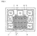
- Fig. 1 shows a compound semiconductor chip of a first embodiment of this invention.
- Switching transistors, FET1 and FET2 are placed at central parts of a GaAs substrate and resistors R1 and R2 are connected to the respective gate electrodes of the FET's.
- electrode pads INPad, OUT1Pad, OUT2Pad, Ctl-1Pad, and Ctl-2Pad, corresponding to the common input terminal, the output terminals, and the control terminals, respectively, are placed at peripheral parts of the substrate.
- An ohmic metal layer (AuGe/Ni/Au) which is in ohmic contact with the substrate, is a first-layer wiring, and forms the source electrodes and drain electrodes of the respective FET's and take-out electrodes of the respective resistors. This layer is not illustrated in Fig. 1 as it overlaps with the pad metal layer.
- a nitride passivation film covers the two FET's as well as the surface of the substrate.
- the nitride film is partially removed to expose the top surface of the GaAs substrate, and posts 71 are formed on the exposed substrate surface at locations shown in Fig. 1.
- a shield metal 70 is supported by the posts 71.
- the shield metal 70 covers the entire area above the FET's and is provided with a plurality of openings, i.e., slits 90 in this embodiment having a width of approximately 2 ⁇ m to 5 ⁇ m and a length of approximately 15 ⁇ m.
- the slits 90 are positioned in the shield metal 70 with a predetermined pattern.
- slits 90 become paths for a resist removal solution in a resist removal step for realizing a hollow structure underneath the shield metal 70, as described above.
- the slits may be of any size or number, and is not limited to those shown in Fig. 1. Bonding wires are press-bonded to the respective electrode pad parts after the removal of the nitride film.
- the structure below the shield metal 70 of the switching circuit device of Fig. 1 is the same as that of Fig. 10.
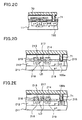
- Figs. 2A and 2B show sectional views of a packaging structure of the chip of Fig. 1 after resin molding.
- Fig. 2A is a sectional view of the packaging
- Fig. 2B is a partially expanded view of Fig. 2A to show the structure around the FET.
- a compound semiconductor chip 63 which is the switching circuit device of Fig. 1, is mounted on an island of lead 62 using a conductive paste 65, and the respective electrode pads of compound semiconductor chip 63 are connected to the leads 62 by bonding wires 64.
- the semiconductor chip 63 is covered by a resin layer 80 that is molded into the packaging shape, and the ends of the leads 62 extend out of the resin layer 80.
- the shield metal 70 is supported by the posts 71 at the positions shown in Fig. 1, and completely covers the area above FET 72.
- the post 71 and the shield metal 70 are formed as one unit.
- the shield metal 70 is formed of a gold plating layer of approximately 2 ⁇ m to 7 ⁇ m.
- the FET 72 and the shield metal 70 are separated by a distance of approximately 1 ⁇ m to 2 ⁇ m. Accordingly, a hollow part 60 is created between the FET 72 and the shield metal 70 as shown in Figs. 2A and 2B, and the surface of the FET, through which high frequency signals pass, is in contact with no substance except the air.
- a resin layer 80 covers the chip 63 and the leads 62.
- the resin does not enter the hollow part 60. Also, though the shield metal 70 is provided with the slits 90, the molding resin does not pass through these slits as long as the slits are 2 ⁇ m to 5 ⁇ m in width as in this embodiment.
- a gate electrode 17 is placed between a source electrode 13 (or drain electrode 15) used for signal input and a drain electrode 15 (or source electrode 13) used for signal output, as shown in Fig. 2B.
- the source electrode 13, the drain electrode 15 and the gate electrode 17 are shielded from the resin layer 80 by the shield metal 70 and the hollow part 60.
- the air contained in the hollow part 60 has an extremely low dielectric constant. Thus, the signal leakage between the source and drain electrodes of the FET that is shut off through the resin layer 80 is effectively prevented.
- the post 71 stands directly on a high impurity region 100 of n+ type, which is formed in the GaAs substrate 11, as shown in Fig. 2C.
- the edge of the high impurity region 100 extends by about 1 ⁇ m from the edge of the post. Because this high impurity region 100 prevents the expansion of a depletion region, which is generated between the drain region or the source region and the area underneath the post 71, the distance d between the post 71 and the drain or source region is as small as 4 ⁇ m and the interference between the post and the FET is still prevented.
- the post 71 may also stand on the exposed GaAs surface, which does not have the high impurity region 100 therein. In this configuration, the distance d between the post 71 and the drain or source region should be 20 ⁇ m or greater. This large distance is required to prevent the interference despite the free extension of the depletion layer.
- the post 71 adheres more firmly to the surface of the GaAs substrate 11 than to dielectric layers, for example a SiNx passivation film, formed on the surface of the GaAs substrate 11. Alloying between the substrate surface and the bottom of the post provides this firm adhesion. A thermal treatment further strengths the bonding between the post 71 and the GaAs substrate 11. As long as the posts 71 do not contact the elements of the switching circuit, the locations of the posts 71 are not limited to those of Fig. 1.
- the configuration of this embodiment is also applicable to a switching circuit device based on a silicon substrate.
- Figs. 2D and 2E show cross-sectional views of examples of such switching circuit devices.
- the device of Fig. 2D is formed on a p+ type substrate 211.
- the device includes a p- type layer 212 formed on the p+ type substrate 211, a source and drain regions 218, 219 of n+ type formed in the p-type layer 212, and two lightly doped regions LD each formed next to the corresponding n+ type regions 218, 219.
- a channel is a region between the two lightly doped regions LD.
- the device also includes a gate oxide layer 213, a gate electrode 217, a source electrode 216, a drain electrode 214 and a passivation film 215.
- the post stands on a p+ type region 100a, which connects to the p+ type substrate 211. Because the substrate 211 is grounded, the post 71 and the shield metal 70 are also grounded through the p+ type region 100a.
- the device of Fig. 2E is the same as that of Fig. 2D except that the post 71 stands on a thick dielectric layer 100b formed in the p- type layer 212.
- this dielectric layer 100b is a SiO2 layer for LOCOS (local oxidation of silicon) separation.
- the post 71 may also stand on a passivation film, such as SiNx, as long as there is no device element formed underneath the pasivation film, which would cause interference through the thin passivation film.
- a punched-out lead frame and a transfer molding are used for the packaging.
- a chip size packaging in which a conductive pattern is formed on an insulating substrate and molding is performed in a batch, is also applicable.
- SPDT switch having a single common input terminal, two FET's and two OUT terminals
- the feature of this embodiment including the hollow structure supported by the shield metal 70 and the resin layer 80, applies to SPDT's with shunt FET's, high-power SPDT's, in which a plurality of FET's are connected in series, DPDT's having two input terminals and two output terminals, and other switching circuit devices as well as switching circuit devices with a GND terminal and a power supply terminal.
- Other switching devices that may be used in this embodiment includes switching circuit devices that use a multi-gate structure FET for high power applications as well as asymmetric SPDT's, SPST's, SP3T's and SP4T's. In fact, this embodiment may be applicable to all the switching devices including those formed on a silicon-based substrate.
- FIG. 3 A semiconductor switching circuit device of a second embodiment of this invention is shown in Figs. 3, 4A, 4B and 4C.
- a shield metal 70 that covers FET's from above extends to and contacts a control terminal electrode pad Ctl-1Pad.
- Figs. 4A, 4B and 4C show sectional views of a packaging structure of the chip shown in Fig. 3. Except the configuration of the shield metal 70, the structure of the switching circuit device of the second embodiment is the same as that of the first embodiment, as shown in Figs. 1, 2A and 2B.
- a part of the shield metal 70 extends toward a control terminal electrode pad Ctl-1Pad, and covers this electrode pad.
- Fig. 4C shows an expanded view of Fig. 4A.
- the control terminal electrode pad Ctl-1Pad is formed of the gate metal layer 20 and the pad metal layer 30, and the shield metal 70 is in direct contact with the pad metal layer 30 of the electrode pad.
- a bonding wire 64 is attached to the shield metal 70.
- the shield metal 70 since a switching operation is performed by applying a control signal of 0V or 3V to the control terminal Ctl-1, a DC potential of 3V or 0V will also be applied to the shield metal 70. Since any DC potential is regarded as a ground potential in terms of high frequency signal applied to the switching device, the source and drain electrodes are shielded by the DC potential from the resin layer 80, which could provide a signal leakage path. In the structure of the first embodiment shown in Fig. 2, the high frequency signals may escape to the resin layer 80 in the form of an electromagnetic field that spreads through the air in the hollow part 60. In this embodiment, however, such a field is prevented from propagating into the resin layer 80 by the shield metal that is connected to the DC potential.
- the shield metal 70 may obviously be put in contact with the control terminal electrode pad Ctl-2 instead. As long as the shield metal 70 is connected with a terminal to which a DC potential is applied, the feature of stopping the electromagnetic field may be accomplished. Thus, the shield metal 70 may be put in contact with a ground terminal electrode pad or a power supply voltage terminal electrode pad when the switching circuit device includes such electrode pads.
- any DC potential may be applied to the shield metal 70 in the device of Fig. 2E because the LOCOS SiO 2 layer effectively prevents the interference between the post and the transistor elements.
- a ground potential should be applied to the shield metal 70 because the shield metal 70 is already at the ground potential.
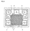
- Fig. 5 shows a semiconductor switching circuit device of a third embodiment of this invention.
- This embodiment has a structure in which a shield metal 70 is not provided with slits.
- a hollow structure is created by placing the shield metal 70 above a resist and thereafter removing the resist.
- slits may be provided in the shield metal 70 as paths for a resist removal solution.
- the resist region to be removed i.e., the hollow part 60
- the resist can be removed without providing slits.
- the shield metal can be disposed over the entire surface without providing slits, and the FET can be shielded completely from the resin layer by the shield metal 70.
- a switching circuit device is formed on a semiconductor substrate as shown in Figs. 6A, 6B and 6C. That is, an FET, having a channel region, source region and drain region, is formed on the semiconductor substrate, and input terminal and output terminal electrode pads, which are connected to the FET, and a terminal electrode pad for applying a DC potential, are formed.
- a compound semiconductor substrate 11 made of GaAs is covered with a silicon nitride film for through-ion implantation to a thickness of approximately 100 ⁇ to 200 ⁇ . Then, ion implantation of a p - -type impurity ( 24 Mg + ) and ion implantation of an n-type impurity ( 29 Si + ) are selectively performed to form a p - -type region on the undoped substrate 11 and an n-type channel layer 12 on top.
- ion implantation of an n+-type impurity ( 29 Si + ) is performed to form a source region 18 and a drain region 19 as well as high impurity regions 160, 161 below a wiring layer 162 and a pad electrode 170, respectively.
- Another high impurity region is formed next to the high impurity region 161 at a location for post construction.
- the source region 18, the drain region 19 and the high impurity regions 160, 161 are formed at the same ion implantation process.
- the high impurity regions 160, 161 are a little larger than the corresponding electrode pad 170 and wiring layer 162, and provides an adequate isolation between the pad electrode 170 and the wiring layer 162 even if these are placed directly on the GaAs substrate. It should be noted that only one tooth of the FET comb structure is shown in the drawings.
- first source electrode 14 and a first drain electrode 16 are vacuum vapor deposited successively to form a first source electrode 14 and a first drain electrode 16 as first-layer electrodes on the source region 18 and drain region 19. Subsequently, ohmic junctions of first source electrode 14 and source region 18 and of first drain electrode 16 and drain region 19 are formed by a heat treatment.
- three layers of Ti/Pt/Au which are to become a gate metal layer, are vacuum vapor deposited successively to form a gate 17, which contacts channel layer 12, a first pad electrode 170 and a wiring layer 162 on the channel layer 12 and the high impurity regions 160, 161, respectively.
- the posts are formed around the FET and the shield metal is formed on the posts.
- a resist PR1 is formed over the entire surface, and a photolithography process of selectively opening windows at regions corresponding to the posts 71 is performed to remove the nitride film and expose the GaAs substrate.
- the high impurity region formed for post construction at the step of Fig. 6A is exposed through the openings of the resist PR1.
- a plating substrate metal 180 three layers of Ti/Pt/Au, for example, are vapor deposited over the entire surface to form a plating substrate metal 180.
- a new resist PR2 is provided and a photolithography process of selectively opening windows at regions in which the shield metal 70 is to be formed is performed. Also, since the slits are to be formed on the shield metal 70, the resist PR2 is left at portions for the formation of the slits. Since the resist PR2 is applied above the plating substrate metal 180, the resist PR2 is separated completely by this plating substrate metal 180 in the vertical direction from the resist PR1.
- Fig. 7C gold plating is applied, photoresist PR2 is removed, and ion milling of the exposed substrate electrode 180 is performed.
- the shield metal 70 which is joined to the posts 71 and practically covers the entire FET 72 from above, is thereby formed.
- the post 71 stands on the impurity region for post construction.
- the slits 90 are also formed at the same time as shown in Fig. 7C.
- the hollow part 60 is formed between the FET 72 and the shield metal 70.
- the slits 90 are provided in the shield metal 70 and these slits 90 are used as paths for the resist removal solution.
- the resist removal solution seeps in from between adjacent posts 71 and from slits 90 and completely removes the resist PR1 below the shield metal.
- the hollow part 60 is thereby formed as shown in Fig. 7D.
- the hollow part 60 above the FET 72 is able to prevent high frequency signals from leaking through the resin layer 80, and thus the hollow part 60 does not have to be thick.
- the thickness of the package exterior does not increase by much and increases only by 2 ⁇ m to 3 ⁇ m in comparison to the conventional device.
- the chip is covered by a resin layer.
- the semiconductor switching circuit device is transferred to an assembly process.
- the wafer having the semiconductor chips is diced and separated into individual semiconductor chips.
- the electrode pads of semiconductor chip 63 and leads 62 are connected by bonding wires.
- Thin gold wires are used as bonding wires 64, and the connections are made by a known ball bonding method.
- transfer molding is performed to provide a resin package to provide the final form, such as shown in Fig. 2A or Fig. 4A.
- the molding resin does not enter the hollow part 60. Since the slits 90 have a width of approximately 2 ⁇ m to 5 ⁇ m, the resin does not enter through these slits 90 either.
- the shield metal 70 supported by the posts 71 the hollow part 60 is formed above the FET by an ordinary resin molding process. The FET 72 and the resin layer 80 are thus shielded by the shield metal 70 and the hollow part 60 containing the air, preventing the leakage of high frequency signals.
- the hollow structure can be obtained just by using a wafer process step of forming a switching circuit element on a wafer, thus providing the advantage of significantly lower cost.
- a method of manufacturing the third embodiment is described with reference to Figs. 8A an 8B.
- the shield metal 70 is not provided with the slits and the FET is covered completely from above by the shield metal 70.
- the shield metal 70 does not have to be provided with the slits. That is, if the area of the shield metal 70 is small, the resist PR1 can be removed adequately with the resist removal solution that seeps in from between adjacent posts 71.
- a photolithography process of selectively opening windows at the post 71 is carried out. After etching the nitride film, the substrate electrode 180 for gold plating is formed. A new resist PR2 is then provided and a photolithography process of selectively opening windows at the shield metal 70 is performed as shown in Fig. 8A.
- the resist PR2 is removed, and ion milling of the exposed substrate electrode is performed.
- the resist layer PR1 is then removed to form the hollow part 60, as shown in Fig. 8B.
- the resin molding is performed to obtain the final structures of the first through third embodiments.
Landscapes
- Junction Field-Effect Transistors (AREA)
- Shielding Devices Or Components To Electric Or Magnetic Fields (AREA)
- Semiconductor Integrated Circuits (AREA)
- Structures Or Materials For Encapsulating Or Coating Semiconductor Devices Or Solid State Devices (AREA)
Applications Claiming Priority (2)
| Application Number | Priority Date | Filing Date | Title |
|---|---|---|---|
| JP2002114959 | 2002-04-17 | ||
| JP2002114959 | 2002-04-17 |
Publications (2)
| Publication Number | Publication Date |
|---|---|
| EP1363331A2 true EP1363331A2 (de) | 2003-11-19 |
| EP1363331A3 EP1363331A3 (de) | 2006-05-17 |
Family
ID=29267331
Family Applications (1)
| Application Number | Title | Priority Date | Filing Date |
|---|---|---|---|
| EP20030009005 Withdrawn EP1363331A3 (de) | 2002-04-17 | 2003-04-17 | Halbleiterschaltvorrichtung und Methode zur Herstellung |
Country Status (3)
| Country | Link |
|---|---|
| US (1) | US6853072B2 (de) |
| EP (1) | EP1363331A3 (de) |
| CN (1) | CN1291492C (de) |
Cited By (2)
| Publication number | Priority date | Publication date | Assignee | Title |
|---|---|---|---|---|
| EP1753024A1 (de) * | 2005-07-11 | 2007-02-14 | Kabushiki Kaisha Toshiba | Halbleiterpackung für hohe Frequenzen |
| EP2083442A1 (de) * | 2008-01-24 | 2009-07-29 | Kabushiki Kaisha Toshiba | Halbleitervorrichtung und Verfahren zur Herstellung der Halbleitervorrichtung |
Families Citing this family (18)
| Publication number | Priority date | Publication date | Assignee | Title |
|---|---|---|---|---|
| US7157385B2 (en) | 2003-09-05 | 2007-01-02 | Micron Technology, Inc. | Method of depositing a silicon dioxide-comprising layer in the fabrication of integrated circuitry |
| US20030062610A1 (en) * | 2001-09-28 | 2003-04-03 | Kovacs Alan L. | Multilayer thin film hydrogen getter |
| TWI236754B (en) * | 2003-04-18 | 2005-07-21 | Phoenix Prec Technology Corp | Method for plating metal layer over isolated pads on substrate for semiconductor package substrate |
| KR100547709B1 (ko) * | 2003-07-07 | 2006-01-31 | 삼성전자주식회사 | 자기 치유 파장분할다중방식 수동형 광 가입자망 |
| WO2006031886A2 (en) * | 2004-09-13 | 2006-03-23 | International Rectifier Corporation | Power semiconductor package |
| US7510966B2 (en) | 2005-03-07 | 2009-03-31 | Micron Technology, Inc. | Electrically conductive line, method of forming an electrically conductive line, and method of reducing titanium silicide agglomeration in fabrication of titanium silicide over polysilicon transistor gate lines |
| JP2010272749A (ja) * | 2009-05-22 | 2010-12-02 | Murata Mfg Co Ltd | 半導体装置 |
| US20120009777A1 (en) | 2010-07-07 | 2012-01-12 | Taiwan Semiconductor Manufacturing Company, Ltd. | UBM Etching Methods |
| US9030841B2 (en) * | 2012-02-23 | 2015-05-12 | Apple Inc. | Low profile, space efficient circuit shields |
| JP5865275B2 (ja) | 2013-01-25 | 2016-02-17 | 株式会社東芝 | 高周波半導体スイッチ |
| US9659717B2 (en) | 2014-02-18 | 2017-05-23 | Analog Devices Global | MEMS device with constant capacitance |
| US9583294B2 (en) | 2014-04-25 | 2017-02-28 | Analog Devices Global | MEMS swtich with internal conductive path |
| US9748048B2 (en) | 2014-04-25 | 2017-08-29 | Analog Devices Global | MEMS switch |
| JP6540528B2 (ja) | 2016-02-04 | 2019-07-10 | 三菱電機株式会社 | 半導体装置及びその製造方法 |
| EP3411894B1 (de) | 2016-02-04 | 2023-06-14 | Analog Devices International Unlimited Company | Aktive öffnende mems-schalter-vorrichtung |
| DE112016007370B4 (de) | 2016-10-24 | 2021-11-11 | Mitsubishi Electric Corporation | Hochfrequenzverstärker |
| DE102018212438A1 (de) * | 2018-07-25 | 2020-01-30 | Infineon Technologies Ag | Halbleitergehäuse mit elektromagnetischer abschirmstruktur und verfahren zu dessen herstellung |
| US20250014659A1 (en) * | 2023-07-03 | 2025-01-09 | Taiwan Semiconductor Manufacturing Company, Ltd. | Read-only memory method, layout, and device |
Family Cites Families (13)
| Publication number | Priority date | Publication date | Assignee | Title |
|---|---|---|---|---|
| JPS63124467A (ja) * | 1986-11-13 | 1988-05-27 | Seiko Epson Corp | 半導体装置 |
| JPH0232546A (ja) * | 1988-07-22 | 1990-02-02 | Hitachi Ltd | 化合物半導体デバイス |
| JPH03218653A (ja) * | 1989-11-13 | 1991-09-26 | Mitsubishi Electric Corp | エアーブリッジ金属配線を具えた半導体装置およびその製造方法 |
| EP0469215B1 (de) * | 1990-07-31 | 1995-11-22 | International Business Machines Corporation | Verfahren zur Herstellung von Bauelementen mit übereinander angeordneten Feldeffekttransistoren mit Wolfram-Gitter und sich daraus ergebende Struktur |
| JPH0817186B2 (ja) * | 1992-03-18 | 1996-02-21 | 三星電子株式会社 | 電界効果トランジスタの製造方法 |
| US5965452A (en) * | 1996-07-09 | 1999-10-12 | Nanogen, Inc. | Multiplexed active biologic array |
| JP2773685B2 (ja) * | 1995-06-16 | 1998-07-09 | 日本電気株式会社 | 半導体装置 |
| JPH09232827A (ja) * | 1996-02-21 | 1997-09-05 | Oki Electric Ind Co Ltd | 半導体装置及び送受信切り替え型アンテナスイッチ回路 |
| JP3831575B2 (ja) * | 2000-05-15 | 2006-10-11 | 三洋電機株式会社 | 化合物半導体スイッチ回路装置 |
| JP2002026035A (ja) * | 2000-07-05 | 2002-01-25 | Hitachi Ltd | 半導体集積回路装置 |
| TWI252582B (en) * | 2001-02-27 | 2006-04-01 | Sanyo Electric Co | Switch circuit device |
| US6472962B1 (en) * | 2001-05-17 | 2002-10-29 | Institute Of Microelectronics | Inductor-capacitor resonant RF switch |
| US6531668B1 (en) * | 2001-08-30 | 2003-03-11 | Intel Corporation | High-speed MEMS switch with high-resonance-frequency beam |
-
2003
- 2003-04-16 US US10/414,490 patent/US6853072B2/en not_active Expired - Lifetime
- 2003-04-17 CN CNB031104886A patent/CN1291492C/zh not_active Expired - Fee Related
- 2003-04-17 EP EP20030009005 patent/EP1363331A3/de not_active Withdrawn
Cited By (5)
| Publication number | Priority date | Publication date | Assignee | Title |
|---|---|---|---|---|
| EP1753024A1 (de) * | 2005-07-11 | 2007-02-14 | Kabushiki Kaisha Toshiba | Halbleiterpackung für hohe Frequenzen |
| US7888797B2 (en) | 2005-07-11 | 2011-02-15 | Kabushiki Kaisha Toshiba | High frequency package device with internal space having a resonant frequency offset from frequency used |
| EP2083442A1 (de) * | 2008-01-24 | 2009-07-29 | Kabushiki Kaisha Toshiba | Halbleitervorrichtung und Verfahren zur Herstellung der Halbleitervorrichtung |
| US8026595B2 (en) | 2008-01-24 | 2011-09-27 | Kabushiki Kaisha Toshiba | Semiconductor device having hermitically sealed active area and electrodes |
| US8476118B2 (en) | 2008-01-24 | 2013-07-02 | Kabushiki Kaisha Toshiba | Semiconductor device and fabrication mehtod of the semiconductor device |
Also Published As
| Publication number | Publication date |
|---|---|
| US20040021156A1 (en) | 2004-02-05 |
| CN1455458A (zh) | 2003-11-12 |
| US6853072B2 (en) | 2005-02-08 |
| CN1291492C (zh) | 2006-12-20 |
| EP1363331A3 (de) | 2006-05-17 |
Similar Documents
| Publication | Publication Date | Title |
|---|---|---|
| US6853072B2 (en) | Semiconductor switching circuit device and manufacturing method thereof | |
| US6777277B2 (en) | Manufacturing method of Schottky barrier diode | |
| US20030025175A1 (en) | Schottky barrier diode | |
| US6891267B2 (en) | Semiconductor switching circuit device | |
| KR100683085B1 (ko) | 반도체 스위치 회로 장치 및 그 제조 방법 | |
| US20050277255A1 (en) | Compound semiconductor device and manufacturing method thereof | |
| EP1265284B1 (de) | Halbleiter-Schaltvorrichtung | |
| EP1538675A1 (de) | Halbleiterbauelement | |
| US7294900B2 (en) | Compound semiconductor device and manufacturing method thereof | |
| US7005688B2 (en) | Semiconductor device with impurity layer to prevent depletion layer expansion | |
| US20050179106A1 (en) | Schottky barrier diode | |
| US6787871B2 (en) | Integrated schottky barrier diode and manufacturing method thereof | |
| KR100621502B1 (ko) | 화합물 반도체 장치의 제조 방법 | |
| EP1265283A2 (de) | Halbleiterschaltanordnung | |
| EP1198006B1 (de) | Verbindungshalbleiterbauelement | |
| JP3702190B2 (ja) | 化合物半導体スイッチ回路装置 | |
| JP2004134434A (ja) | スイッチ回路装置および化合物半導体装置の製造方法 | |
| CN100487895C (zh) | 化合物半导体装置 | |
| JP2004186537A (ja) | スイッチ回路装置および化合物半導体装置の製造方法 | |
| JP2001332555A (ja) | 化合物半導体装置の製造方法 | |
| JP2002118121A (ja) | 化合物半導体装置の製造方法 | |
| JP2004134433A (ja) | スイッチ回路装置および化合物半導体装置の製造方法 | |
| JP2004134588A (ja) | 半導体装置の製造方法 | |
| JP2003007725A (ja) | 化合物半導体装置の製造方法 | |
| JP2002231897A (ja) | 化合物半導体スイッチ回路装置 |
Legal Events
| Date | Code | Title | Description |
|---|---|---|---|
| PUAI | Public reference made under article 153(3) epc to a published international application that has entered the european phase |
Free format text: ORIGINAL CODE: 0009012 |
|
| AK | Designated contracting states |
Kind code of ref document: A2 Designated state(s): AT BE BG CH CY CZ DE DK EE ES FI FR GB GR HU IE IT LI LU MC NL PT RO SE SI SK TR |
|
| AX | Request for extension of the european patent |
Extension state: AL LT LV MK |
|
| RIC1 | Information provided on ipc code assigned before grant |
Ipc: H01L 23/528 20060101ALI20060112BHEP Ipc: H01L 23/552 20060101ALI20060112BHEP Ipc: H01L 23/485 20060101ALI20060112BHEP Ipc: H01L 23/66 20060101AFI20060112BHEP |
|
| PUAL | Search report despatched |
Free format text: ORIGINAL CODE: 0009013 |
|
| AK | Designated contracting states |
Kind code of ref document: A3 Designated state(s): AT BE BG CH CY CZ DE DK EE ES FI FR GB GR HU IE IT LI LU MC NL PT RO SE SI SK TR |
|
| AX | Request for extension of the european patent |
Extension state: AL LT LV MK |
|
| 17P | Request for examination filed |
Effective date: 20060908 |
|
| AKX | Designation fees paid |
Designated state(s): DE |
|
| STAA | Information on the status of an ep patent application or granted ep patent |
Free format text: STATUS: THE APPLICATION IS DEEMED TO BE WITHDRAWN |
|
| 18D | Application deemed to be withdrawn |
Effective date: 20101103 |