EP1345262B1 - Method for producing silicon wafer and silicon wafer - Google Patents
Method for producing silicon wafer and silicon wafer Download PDFInfo
- Publication number
- EP1345262B1 EP1345262B1 EP01998993.8A EP01998993A EP1345262B1 EP 1345262 B1 EP1345262 B1 EP 1345262B1 EP 01998993 A EP01998993 A EP 01998993A EP 1345262 B1 EP1345262 B1 EP 1345262B1
- Authority
- EP
- European Patent Office
- Prior art keywords
- thermal annealing
- silicon wafer
- silicon
- oxide film
- atmosphere
- Prior art date
- Legal status (The legal status is an assumption and is not a legal conclusion. Google has not performed a legal analysis and makes no representation as to the accuracy of the status listed.)
- Expired - Lifetime
Links
- 229910052710 silicon Inorganic materials 0.000 title claims description 223
- XUIMIQQOPSSXEZ-UHFFFAOYSA-N Silicon Chemical compound [Si] XUIMIQQOPSSXEZ-UHFFFAOYSA-N 0.000 title claims description 221
- 239000010703 silicon Substances 0.000 title claims description 221
- 238000004519 manufacturing process Methods 0.000 title claims description 38
- 235000012431 wafers Nutrition 0.000 claims description 192
- 238000000137 annealing Methods 0.000 claims description 146
- 239000007789 gas Substances 0.000 claims description 47
- 150000004767 nitrides Chemical class 0.000 claims description 47
- 230000007547 defect Effects 0.000 claims description 41
- QVGXLLKOCUKJST-UHFFFAOYSA-N atomic oxygen Chemical compound [O] QVGXLLKOCUKJST-UHFFFAOYSA-N 0.000 claims description 39
- 239000001301 oxygen Substances 0.000 claims description 39
- 229910052760 oxygen Inorganic materials 0.000 claims description 39
- 239000010410 layer Substances 0.000 claims description 36
- 238000011282 treatment Methods 0.000 claims description 31
- 238000006243 chemical reaction Methods 0.000 claims description 17
- 239000002344 surface layer Substances 0.000 claims description 9
- 206010037544 Purging Diseases 0.000 claims description 7
- 238000010926 purge Methods 0.000 claims description 7
- 238000000354 decomposition reaction Methods 0.000 claims description 6
- 125000004430 oxygen atom Chemical group O* 0.000 claims 1
- 239000010408 film Substances 0.000 description 91
- QGZKDVFQNNGYKY-UHFFFAOYSA-N Ammonia Chemical compound N QGZKDVFQNNGYKY-UHFFFAOYSA-N 0.000 description 51
- 229910000069 nitrogen hydride Inorganic materials 0.000 description 41
- 238000005121 nitriding Methods 0.000 description 27
- 230000000694 effects Effects 0.000 description 23
- 238000002347 injection Methods 0.000 description 19
- 239000007924 injection Substances 0.000 description 19
- 239000002244 precipitate Substances 0.000 description 16
- 238000001816 cooling Methods 0.000 description 11
- IJGRMHOSHXDMSA-UHFFFAOYSA-N Atomic nitrogen Chemical compound N#N IJGRMHOSHXDMSA-UHFFFAOYSA-N 0.000 description 10
- 230000003247 decreasing effect Effects 0.000 description 8
- 238000000034 method Methods 0.000 description 8
- 239000013078 crystal Substances 0.000 description 7
- 230000003746 surface roughness Effects 0.000 description 7
- 230000015572 biosynthetic process Effects 0.000 description 6
- 238000005247 gettering Methods 0.000 description 6
- 229910021529 ammonia Inorganic materials 0.000 description 5
- 238000004140 cleaning Methods 0.000 description 5
- 230000007423 decrease Effects 0.000 description 5
- 238000010438 heat treatment Methods 0.000 description 5
- 229910052757 nitrogen Inorganic materials 0.000 description 5
- 238000001556 precipitation Methods 0.000 description 5
- 230000001376 precipitating effect Effects 0.000 description 4
- VYPSYNLAJGMNEJ-UHFFFAOYSA-N Silicium dioxide Chemical compound O=[Si]=O VYPSYNLAJGMNEJ-UHFFFAOYSA-N 0.000 description 3
- 238000007796 conventional method Methods 0.000 description 3
- 239000001257 hydrogen Substances 0.000 description 3
- 229910052739 hydrogen Inorganic materials 0.000 description 3
- KRHYYFGTRYWZRS-UHFFFAOYSA-N Fluorane Chemical compound F KRHYYFGTRYWZRS-UHFFFAOYSA-N 0.000 description 2
- OAKJQQAXSVQMHS-UHFFFAOYSA-N Hydrazine Chemical compound NN OAKJQQAXSVQMHS-UHFFFAOYSA-N 0.000 description 2
- UFHFLCQGNIYNRP-UHFFFAOYSA-N Hydrogen Chemical compound [H][H] UFHFLCQGNIYNRP-UHFFFAOYSA-N 0.000 description 2
- 229910020776 SixNy Inorganic materials 0.000 description 2
- 238000001514 detection method Methods 0.000 description 2
- 238000009826 distribution Methods 0.000 description 2
- 238000005530 etching Methods 0.000 description 2
- 238000001704 evaporation Methods 0.000 description 2
- 239000012535 impurity Substances 0.000 description 2
- 238000005259 measurement Methods 0.000 description 2
- 229910021421 monocrystalline silicon Inorganic materials 0.000 description 2
- 230000003647 oxidation Effects 0.000 description 2
- 238000007254 oxidation reaction Methods 0.000 description 2
- 238000004151 rapid thermal annealing Methods 0.000 description 2
- 150000003376 silicon Chemical class 0.000 description 2
- 229910052814 silicon oxide Inorganic materials 0.000 description 2
- 238000007669 thermal treatment Methods 0.000 description 2
- DIIIISSCIXVANO-UHFFFAOYSA-N 1,2-Dimethylhydrazine Chemical compound CNNC DIIIISSCIXVANO-UHFFFAOYSA-N 0.000 description 1
- GQPLMRYTRLFLPF-UHFFFAOYSA-N Nitrous Oxide Chemical compound [O-][N+]#N GQPLMRYTRLFLPF-UHFFFAOYSA-N 0.000 description 1
- 229910002790 Si2N2O Inorganic materials 0.000 description 1
- 229910052581 Si3N4 Inorganic materials 0.000 description 1
- 230000015556 catabolic process Effects 0.000 description 1
- 230000006837 decompression Effects 0.000 description 1
- 230000001419 dependent effect Effects 0.000 description 1
- 238000009792 diffusion process Methods 0.000 description 1
- AZLYZRGJCVQKKK-UHFFFAOYSA-N dioxohydrazine Chemical compound O=NN=O AZLYZRGJCVQKKK-UHFFFAOYSA-N 0.000 description 1
- 230000008020 evaporation Effects 0.000 description 1
- 238000002474 experimental method Methods 0.000 description 1
- 150000002431 hydrogen Chemical class 0.000 description 1
- 125000004435 hydrogen atom Chemical group [H]* 0.000 description 1
- 239000000203 mixture Substances 0.000 description 1
- 230000003287 optical effect Effects 0.000 description 1
- 230000001590 oxidative effect Effects 0.000 description 1
- 238000012545 processing Methods 0.000 description 1
- 239000000047 product Substances 0.000 description 1
- 239000010453 quartz Substances 0.000 description 1
- 239000004065 semiconductor Substances 0.000 description 1
- 230000035945 sensitivity Effects 0.000 description 1
- HBMJWWWQQXIZIP-UHFFFAOYSA-N silicon carbide Chemical compound [Si+]#[C-] HBMJWWWQQXIZIP-UHFFFAOYSA-N 0.000 description 1
- 229910010271 silicon carbide Inorganic materials 0.000 description 1
- 238000004088 simulation Methods 0.000 description 1
- 238000004544 sputter deposition Methods 0.000 description 1
- 230000006641 stabilisation Effects 0.000 description 1
- 238000011105 stabilization Methods 0.000 description 1
- 238000003756 stirring Methods 0.000 description 1
- 238000000859 sublimation Methods 0.000 description 1
- 230000008022 sublimation Effects 0.000 description 1
- 239000000126 substance Substances 0.000 description 1
- 230000001629 suppression Effects 0.000 description 1
- 238000010301 surface-oxidation reaction Methods 0.000 description 1
- 239000010409 thin film Substances 0.000 description 1
Images


Classifications
-
- H—ELECTRICITY
- H01—ELECTRIC ELEMENTS
- H01L—SEMICONDUCTOR DEVICES NOT COVERED BY CLASS H10
- H01L21/00—Processes or apparatus adapted for the manufacture or treatment of semiconductor or solid state devices or of parts thereof
- H01L21/02—Manufacture or treatment of semiconductor devices or of parts thereof
- H01L21/04—Manufacture or treatment of semiconductor devices or of parts thereof the devices having potential barriers, e.g. a PN junction, depletion layer or carrier concentration layer
- H01L21/18—Manufacture or treatment of semiconductor devices or of parts thereof the devices having potential barriers, e.g. a PN junction, depletion layer or carrier concentration layer the devices having semiconductor bodies comprising elements of Group IV of the Periodic Table or AIIIBV compounds with or without impurities, e.g. doping materials
- H01L21/30—Treatment of semiconductor bodies using processes or apparatus not provided for in groups H01L21/20 - H01L21/26
- H01L21/324—Thermal treatment for modifying the properties of semiconductor bodies, e.g. annealing, sintering
-
- H—ELECTRICITY
- H01—ELECTRIC ELEMENTS
- H01L—SEMICONDUCTOR DEVICES NOT COVERED BY CLASS H10
- H01L21/00—Processes or apparatus adapted for the manufacture or treatment of semiconductor or solid state devices or of parts thereof
- H01L21/02—Manufacture or treatment of semiconductor devices or of parts thereof
- H01L21/04—Manufacture or treatment of semiconductor devices or of parts thereof the devices having potential barriers, e.g. a PN junction, depletion layer or carrier concentration layer
- H01L21/18—Manufacture or treatment of semiconductor devices or of parts thereof the devices having potential barriers, e.g. a PN junction, depletion layer or carrier concentration layer the devices having semiconductor bodies comprising elements of Group IV of the Periodic Table or AIIIBV compounds with or without impurities, e.g. doping materials
- H01L21/30—Treatment of semiconductor bodies using processes or apparatus not provided for in groups H01L21/20 - H01L21/26
- H01L21/322—Treatment of semiconductor bodies using processes or apparatus not provided for in groups H01L21/20 - H01L21/26 to modify their internal properties, e.g. to produce internal imperfections
- H01L21/3221—Treatment of semiconductor bodies using processes or apparatus not provided for in groups H01L21/20 - H01L21/26 to modify their internal properties, e.g. to produce internal imperfections of silicon bodies, e.g. for gettering
- H01L21/3225—Thermally inducing defects using oxygen present in the silicon body for intrinsic gettering
Definitions
- the present invention relates to a production method for silicon wafers comprising the steps of forming vacancies in a silicon wafer by thermal annealing in atmosphere and forming a denuded zone (DZ) layer just under the surface of the silicon wafer by further thermal annealing.
- DZ denuded zone
- Silicon wafers produced by processing single crystal silicon which is obtained by pulling up and growing by Czochralski (CZ) method contain many oxygen impurities, and the oxygen impurities generate oxygen precipitates (BMD: bulk micro defect) causing dislocation, defects, or the like.
- BMD bulk micro defect
- thermal annealing RTA: rapid thermal annealing
- rapid heating at high-temperature of 1250°C or higher for a short time and rapid cooling is carried out on silicon wafers in the predetermined atmosphere to form vacancies with high concentration in thermal equilibrium in the silicon wafer.
- a DZ layer a non-defect layer is uniformly formed (for example, as disclosed in WO 98/38675 ).
- thermal annealing in an oxygen atmosphere is carried out on the silicon wafer, and subsequently, the thermal annealing in a non-oxidizing atmosphere is carried out, to form a DZ layer near the surface and a BMD in the silicon wafer.
- N 2 nitrogen
- Si x N y nitride film
- the thermal annealing for forming vacancies is carried out in the atmosphere mainly containing N 2 after covering the surface of the silicon wafer with an oxide film.
- thermal annealing at 1250°C or higher for 10 seconds or more is necessary.
- slips are generated from parts being in contact with a susceptor, supporting pins, or the like by the thermal annealing at high temperature in the silicon wafer. These slips may cause cracks or the like.
- a natural oxide film is formed on the surface of the silicon wafer before thermal annealing.
- the natural oxide film on the surface of the silicon wafer sublimates during the above thermal annealing at high temperature, so that the surface of the silicon wafer becomes rough.
- the present invention has been made to solve the above problems and an object thereof is the provision of a production method for silicon wafers and a silicon wafer wherein a first thermal annealing is carried out at low temperature or for short time to suppress generation of slip and to provide satisfactory surface roughness.
- the present invention provides a production method for silicon wafers as defined in the appended Claim 1.
- the atmosphere used in the first thermal annealing step comprises nitride gas as specified in the claims, namely, comprising NH 3 having a lower decomposition temperature than the decomposable temperature of N 2 .
- the thermal annealing is carried out at lower thermal annealing temperature or for shorter time than the thermal annealing temperature or thermal annealing time of N 2 .
- the nitride gas is decomposed to form a nitride film on the surface of the silicon wafer.
- vacancies can be injected into the silicon wafer and the generation of slips in the thermal annealing can be suppressed.
- the above nitride gas comprises NH 3 (ammonia).
- NH 3 ammonia
- the use of the nitride gas comprising NH 3 in the production method for silicon wafers enhances nitriding of the silicon wafer surface and injection of vacancies, because H (hyckrogen) generated by decomposition of NH 3 has a cleaning effect that H strips the natural oxide film and the like on the surface of the silicon wafer.
- NH 3 has an effect of nitriding the oxide film, as a result, and the injection of vacancies in the silicon wafer is accelerated.
- the cleaning effect of NH 3 is not due to evaporation (sublimation) of the natural oxide film at high temperatures but due to deoxidation by hydrogen.
- a concentration of NH 3 in the above nitride gas is 0.5% or more or the flow rate of NH 3 is 10 sccm or more.
- the nitriding reaction is the reaction rate determinater. As long as the atmosphere comprises the nitride gas in this condition, the thickness of the nitride film formed on the surface of the silicon wafer is uniform, so that injection of vacancies into the silicon wafer can be uniformly carried out.
- the above nitride gas may be a plasmatic nitride gas. Since the plasmatic nitride gas is activated, nitriding of the surface of the silicon wafer and injection of vacancies in the silicon wafer is further accelerated.
- the annealing temperature in the first thermal annealing step is within 900°C to 1200°C and the annealing time is up to 60 seconds or shorter. According to the above range of thermal annealing temperature and thermal annealing time, generation of slips can be suppressed and a sufficient amount of vacancies can be injected in order to obtain suitable amount of BMD layer. Moreover, as described later, since the thermal annealing is carried out at 1200°C or lower, less interstitial silicon is formed in the crystal. Therefore, pair annihilation between vacancies injected by the nitriding of the silicon wafer surface and interstitial silicon does not occur, so that injection efficiency is increased.
- the production method for silicon wafers according to the present invention comprises an oxide film stripping step for stripping or thinning the oxide film on the surface of the silicon wafer before the first thermal annealing step. Since the production method for silicon wafers according to the present invention comprises an oxide film stripping step for stripping or thinning the oxide film on the surface of the silicon wafer before the thermal annealing step, the RTA is carried out under the condition in which the oxide film such as natural oxide film on the surface of the silicon wafer is completely or nearly completely stripped. As a result, it can promote nitriding of the surface of the silicon wafer by the nitride gas and injection of vacancies without disturbance by the oxide film, and the injection of vacancies is effectively carried out.
- the oxide film is thinned so as to be less than 2 nm thick in the oxide film stripping step in case where the thickness of the oxide film is 2 nm or more.
- the present inventors found, as described later, that when the oxide film is formed with a thickness of 2 nm or more on the surface of the silicon wafer, the oxide film cannot be completely stripped or cannot be sufficiently converted to an oxynitride film during the thermal annealing (thermal annealing temperature is 900°C to 1200°C and thermal annealing time is up to 60 seconds). As a result, the sufficient effect of injection of vacancies cannot be obtained.
- the oxide film stripping step in the production method for silicon wafers since the oxide film is thinned so as to be less than 2 nm thick and the atmosphere comprises NH 3 , as described later, the remaining oxide film is sufficiently converted to an oxynitride film and a sufficient effect of injection of vacancies is obtained.
- the silicon wafer in the first thermal annealing step, is provided in a reaction chamber for the first thermal annealing, and an atmosphere comprising nitride gas is supplied into the reaction chamber after a purging treatment for removing oxygen contained in an atmosphere in the reaction chamber.
- the atmosphere comprising nitride gas since the atmosphere comprising nitride gas is supplied into the reaction chamber after a purging treatment for removing oxygen contained in an atmosphere in the reaction chamber, the atmosphere does not comprise oxygen so as to prevent suppression of the effect of injection of vacancies by surface oxidation.
- the production method for silicon wafers according to the present invention comprises a second thermal annealing step for forming a DZ layer on the surface layer of the silicon wafer at lower temperature than that in the thermal annealing step, and at the same time a precipitation treatment step for precipitating oxygen in vacancies in the silicon wafer, after the first thermal annealing step.
- the present invention comprises a forming step for forming a DZ layer just under the silicon wafer surface at lower temperature than that in the first thermal annealing step, and a precipitation treatment step for precipitating oxygen for utilizing the vacancies in the silicon wafer, after the first thermal annealing step, a high quality silicon wafer having a DZ layer, which is suitable for forming a device, as the surface layer, and also having a high BMD density area having a proximity gettering effect therein can be prepared.
- a silicon wafer according to the present invention is provided with vacancies therein by the first thermal annealing and is produced by the above production method for silicon wafers according to the present invention. Since the silicon wafer is produced by the above production method for silicon wafers according to the present invention, generation of slips is suppressed, and a high quality silicon wafer, which contains a DZ layer having sufficient thickness, and suitably high BMD density therein by the thermal annealing, is obtained.
- the silicon wafer according to the present invention is provided with vacancies therein by the first thermal annealing, its surface may comprise a silicon oxynitride film formed by nitriding the surface thereof during the thermal annealing. Since the silicon wafer comprises a silicon oxynitride film formed by nitriding the surface thereof during the thermal annealing, that is, a silicon oxynitride film formed by nitriding the surface without evaporating a silicon oxide film such as a natural oxide film or oxygen during the thermal annealing, sufficient vacancies are injected into the silicon wafer by nitriding the surface and satisfactory surface roughness is exhibited with suppressing roughness of the surface. Therefore,the second thermal annealing for oxygen precipitates to the silicon wafer produces a silicon wafer containing a BMD layer having high BMD density therein and a DZ layer having good surface roughness as a surface layer.
- the silicon wafer according to the present invention a method for forming a non-defect layer as at least a surface layer and precipitating oxygen in the above vacancies in the silicon wafer is adopted. Since a non-defect layer as at least a surface layer is formed and oxygen is precipitated by utilizing the vacancies in the silicon wafer, the silicon wafer comprises a preferable DZ layer as a device formed area and a BMD area having sufficient BMD density in the silicon wafer, and can exhibit the proximity gettering effect.
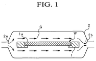
- Fig. 1 is a single-type thermal annealing furnace for conducting a production method for silicon wafers according to the present invention.
- the thermal annealing furnace comprises annular susceptor 1 on which silicon wafer W can be provided, and reaction chamber 2 in which susceptor 1 is equipped. Furthermore, a lamp (not shown) is provided at the outside of reaction chamber 2 to heat the silicon wafer W.
- Susceptor 1 is composed of a silicon carbide and the like, step portion 1a is provided in susceptor 1, and circumferential edge of silicon wafer W is provided on step portion 1a.
- reaction chamber 2 supply port 2a, which supplies atmosphere G on the surface of silicon wafer W, and discharge port 2b, which discharges supplied atmosphere G, are provided.
- supply port 2a is connected to a supply source (not shown) of atmosphere G.
- Atmosphere G is a nitride gas comprising NH 3 having lower decomposition temperature than N 2 decomposable temperature, or a mixed gas NH 3 with NO, N 2 O, N 2 O 2 , hydrazine, dimethylhydrazine and the like, or a mixed gas of NH 3 with at least one of these nitride gasses and Ar, N 2 , H 2 , or the like.
- atmosphere G preferably mainly comprises NH 3 .
- a method for forming new vacancies in the silicon wafer W by RTA treatment (rapid thermal annealing) of the silicon wafer W in the atmosphere in the thermal annealing furnace, and then a method of the second thermal annealing for forming a DZ layer on the surface of silicon wafer W and at the same time, forming a BMD layer in the silicon wafer W, are explained as follows. First, a natural oxide film formed on the surface of silicon wafer W or an oxide film, which is generated by other treatments, is stripped or is treated to be a thin film before RTA treatment for injecting vacancies, in case the thickness of the oxide film is 2 nm or more.
- the silicon wafer W before thermal annealing is washed by hydrofluoric acid or the like to strip the oxide film on the surface of silicon wafer W beforehand.
- the oxide film is thinned so as to be 2 nm thick.
- stripping treatment of the oxide film is not necessary, as described below.
- the silicon wafer W is provided on susceptor 1, and then thermal annealing of rapid heating and rapid cooling (for example, increasing or decreasing temperature with 50°C/sec) for a short time at thermal annealing within 900°C to 1200°C for 60 sec or less during supplying the above atmosphere G from supply port 2a to the surface of silicon wafer W.
- This thermal annealing includes a spike annealing in which thermal annealing is carried out for a short time (less than 1 second).
- RTA treatment is carried out at further preferable conditions, that is, thermal annealing temperature of 900 to 1180°C and thermal annealing time of 30 sec or shorter.
- purging treatment is carried out for stripping oxygen by supplying a large amount of Ar into the thermal annealing furnace as an atmosphere to replace the atmosphere in the thermal annealing furnace before heating to 800°C. Subsequently, the silicon wafer W is heated to 800C while a predetermined current amount of Ar as the atmosphere is supplied.
- the predetermined amount of NH 3 is introduced into the thermal annealing furnace to mix with Ar for supplying a mixed gas of Ar and NH 3 as the atmosphere, rapid heating treatment is carried out to be the predetermined thermal annealing temperature (for example, 1180°C) from 800°C, thermal annealing is carried out for the predetermined time at the thermal annealing temperature maintained regularly, and then rapid cooling is carried out to be 800°C.
- the predetermined thermal annealing temperature for example, 1180°C
- thermal annealing is carried out for the predetermined time at the thermal annealing temperature maintained regularly, and then rapid cooling is carried out to be 800°C.
- the larger amount of Ar gas is supplied to susceptor 1 as the atmosphere with maintaining the temperature of 800°C to completely substitute for NH 3 , and then the temperature is decreased in the atmosphere of only Ar gas after exhaustion of NH 3 is completed.
- nitride gas having low decomposition temperature is supplied as the atmosphere from a certain point during increase of temperature to a certain point during rapid decrease of temperature.
- the thermal annealing temperature during the introduction of NH 3 gas is equal to the temperature (800°C) during the purging treatment after the first thermal annealing in order to relieve a load on the apparatus.
- rapid cooling is carried out by taking silicon wafer W out of the thermal annealing furnace.
- the rapid cooling effect when the thermal annealing (800°C) is carried out in the purging treatment and silicon wafer W is taken out makes it possible for oxygen donors in the silicon wafer to be stripped.
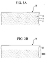
- the surface of silicon wafer W undergoes nitriding by sufficiently decomposing a nitride gas at lower thermal annealing temperature than the conventional thermal annealing temperature, that is, a nitride film is formed on the surface of silicon wafer W, and then vacancies V are sufficiently injected into silicon wafer W, as shown in Fig. 3A .
- a second thermal annealing at 800°C for four hours under N 2 /O 2 atmosphere is carried out in the thermal annealing furnace or the like after the RTA treatment. Accordingly, as shown in Fig. 3B , a denuded zone of a DZ layer is formed just under the silicon wafer surface by pair annihilation of vacancies which diffuse to the surface and interstitial silicons which are injected by formation of the oxide film, and while oxygen precipitate nuclei are stabilized.
- the second thermal annealing for longer time for example, a thermal annealing at 1000°C for 16 hours, is carried out, oxygen precipitates grow and the BMD layer having high BMD density is formed therein.
- DZ layer and oxygen precipitates may be carried out in a second thermal annealing during a device preparing step.
- the atmosphere G is a nitride gas comprising NH 3 having a lower temperature than the decomposable temperature of N 2 , the thermal annealing temperature in the RTA treatment can be lower temperature and generation of slip during the thermal annealing can be suppressed.
- atmosphere G mainly composed by NH 3
- a cleaning effect for stripping natural oxide films and the like on the surface of silicon wafer W by hydrogen atom H generated by decomposing NH 3 occurs, so that nitriding and injection of vacancies V are accelerated. Furthermore, since NH 3 has a nitriding effect on oxide film, injection of vacancies V is accelerated.
- the thermal annealing is carried out within 900° to 1200°C for 60 seconds or less, generation of slip can be suppressed and vacancies V can be sufficiently injected to obtain suitable amounts of BMD layer.
- the first thermal annealing is carried out at a low temperature of 1200°C or less to decrease generation of Frenkel pairs, the amount of interstitial silicons formed in crystal is decreased; and vacancies, which are injected by a nitride film formed on the surface of silicon crystal, and interstitial silicons are not pair-annihilated, and injection efficiency of vacancies can be increased and vacancies V can be injected deeply into the crystal.
- oxide film on the surface of silicon wafer W is stripped or thinned, if needed as explained above, the RTA treatment is carried out under the condition in which oxide films such as natural oxide films on the surface of wafer W are completely or nearly completely stripped.
- oxide films such as natural oxide films on the surface of wafer W are completely or nearly completely stripped.
- disturbance of nitriding and vacancy injection at the surface of wafer W using nitride gas by oxide films can be prevented, and effective injection of vacancies can be carried out.
- the oxide film is thinned so as to be less than 2 nm thick, the remained oxide film can be stripped or be an oxynitride film by cleaning effect or nitriding effect of NH 3 , and vacancies V can be sufficiently injected.
- a second thermal annealing is carried out on silicon wafer W at lower temperature than the temperature in the above first thermal annealing to form a denuded zone of the DZ layer just under the surface, and at the same time, to form a bulk micro defect of the BMD layer by precipitating oxygen by utilizing the vacancies V in the silicon wafer.
- the first thermal annealing temperature is decreased in comparison with a conventional example.
- the above plasmatic nitride gas may be used as an atmosphere.
- the plasmatic nitride gas is activated, nitriding of the surface of the silicon wafer and injection of vacancies into the silicon wafer is further accelerated.
- the atmosphere is a mixed gas composed of three kind gasses
- one or more of the gasses are nitride gases comprising NH 3 .
- the atmosphere is a mixed gas composed of two kind gases
- the NH 3 in the nitride gas contained in the mixed gas has an amount of 0.5% or more, or 10 sccm or more based on the absolute amount.
- the nitriding reaction in this range is a rate determination. As long as the mixed gas contains the nitride gas having the minimum amount or more, each nitride film formed on the surface of the silicon wafer has the same film thickness. As a result, each concentration of vacancies to be introduced and each amount of precipitation are the same.
- the nitriding reaction in this range is a diffusion control, and the precipitation amount of oxygen is controlled by controlling the amount of nitrogen.
- the pressure of the atmosphere can be any of decompression, normal pressure, and pressurizing.
- the nitride film and the oxynitride film (silicon nitride-oxide film) formed on the surface of the silicon wafer in the above embodiment is Si x N y such as Si 3 N 4 .
- Si 2 N x O y such as Si 2 N 2 O is formed, that is, a silicon oxide-nitride film is formed.
- This silicon oxide-nitride film is formed by nitriding a natural oxide film, chemical oxide film, or thermal oxide film.
- These nitride films may further contain hydrogen in the films.
- natural oxide films may be formed on the surface of a silicon wafer before thermal annealing treatment. Even if there are the oxide films such as natural oxide films, a sufficient vacancy injection effect can be obtained by a cleaning effect using NH 3 or the like, or by nitriding of oxide films.
- an oxide film which has a greater thickness than that of a natural oxide film be actively formed on the surface of the silicon wafer before the thermal annealing using the above nitride gas comprising NH 3 in the present embodiment, and a process such as a thermal annealing in atmosphere containing oxygen is carried out before the first thermal annealing using the above nitride gas comprising NH 3 .
- the purging treatment for removing oxygen contained in the atmosphere is carried out before supplying the above nitride gas such as NH 3 to the reaction chamber.
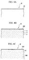
- a natural oxide film (silicon oxide film, SO) is formed on the surface of silicon wafer W before the first thermal annealing, and oxide film stripping treatment is not particularly carried out.
- the above-described RTA treatment is carried out so that the natural oxide film (SO) and silicon on the surface of silicon wafer W is nitrided by NH 3 , and accordingly, as shown Fig. 4B , vacancies V are injected into silicon wafer W, and a silicon nitride-oxide film (SNO) is formed on the surface of silicon wafer W.
- the silicon wafer Since the silicon wafer has an oxynitride film formed by nitriding the surface thereof in the first thermal annealing, that is, has a silicon nitride-oxide film SNO formed by nitriding a natural oxide film SO on the surface thereof in the thermal annealing, the silicon wafer comprises sufficient vacancies V injected therein by nitriding the surface thereof and satisfactory surface roughness which is suitably suppressed. If the second thermal annealing for oxygen precipitates is carried out to the silicon wafer, as shown in Fig. 4C , a silicon wafer containing a BMD of a BMD layer having high BMD density therein and a DZ of a DZ layer having satisfactory surface roughness can be obtained.
- silicon wafers processed by slicing ingots which are obtained by pulling up and growing by normal CZ method, are used in the above embodiment; however, silicon wafers processed by slicing ingots, which are obtained by pulling up and growing by another CZ method, may be used.
- silicon wafers in which there is no agglomerate of point defects processed by slicing ingots composed of perfect area [P] are used, when an area where interstitial silicon type point defects mainly exist, is defined as area [I], an area where vacancy type point defects mainly exist, is defined as area [V], and an area where agglomerate of interstitial silicon type point defects and agglomerate of vacancy type point defects exist, is defined as perfect area [P] in silicon single crystal ingots.
- the vacancy type point defect is a defect formed by a vacancy generated by being displaced a silicon atom from a silicon lattice site
- the interstitial silicon type point defect is a defect in which a silicon atom is in a position other than a lattice point of the silicon crystal (interstitial site).
- the silicon wafer composed of perfect area [P] is, for example, as suggested in Japanese Unexamined Patent Application, First Publication No. 1-001393 , produced by pulling up ingots from a molten silicon in a hot zone according to a CZ method with the pulling rate profile based on Voronkov theory, and subsequently, slicing these ingots.
- the ingots are made with determining a value of V/G (mm 2 /min.
- °C so as to annihilate oxidation induced stacking faults (OSFs) in the center of silicon wafer, which are generated like rings by the thermal oxidation treatment, where pulling rate is V (mm/min) and temperature gradient in the vertical direction of the ingots near the interface between the molten silicon and the ingots in a crucible is G (°C/mm).
- pulling rate is V (mm/min)
- temperature gradient in the vertical direction of the ingots near the interface between the molten silicon and the ingots in a crucible is G (°C/mm).
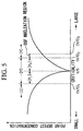
- the above-described Voronkov theory schematically expresses a relationship between V/G and point defect concentration when V/G is plotted on the horizontal axis and vacancy type point defect concentration and interstitial silicon type defect concentration are plotted on the vertical axis, and explains that the interface between a vacancy area and interstitial silicon area is determined according to the value of V/G.
- V/G ratio is more than the critical point
- ingots having rich vacancy type point defect concentration are formed.
- V/G ratio is less than the critical point, ingots having rich interstitial silicon type point defect concentration are formed.
- [I] where the interstitial silicon type point defects richly exist indicates the area where agglomerates of interstitial silicon type point defects exist (area of smaller than (V/G) 1 )
- [V] where the vacancy type point defects richly exist indicates the area where agglomerates of vacancy type point defects exist (area of larger than (V/G) 2 )
- [P] indicates the perfect area where no agglomerate of interstitial silicon type point defects and no agglomerate of vacancy type point defects exist (area between (V/G) 1 and (V/G) 2 ).
- the area [V] adjacent to the area [P] comprises an area [OSF] (area between (V/G) 2 and (V/G) 3 ) in which OSF nuclei are formed.
- the pulling rate profile of ingots to be silicon wafers is determined so that the ratio (V/G) of pulling rate to temperature gradient is the first critical ratio ((V/G) 1 ) or larger to prevent generation of agglomerates of interstitial silicon type point defects, and is the second critical ratio ((V/G) 2 ) or smaller to suppress agglomerate of vacancy type point defects within the area where numerous vacancy type point defects exist in the center of the ingot.
- the pulling rate profile is determined by experimentally slicing a reference ingot in the axial direction and numerical simulations based on Voronkov theory.
- the silicon wafer produced in the perfect area [P] becomes a silicon wafer having no defect such as OSF and COP. Since this silicon wafer has low IG (intrinsic or internal gettering) effect, if the thermal annealing according to the above-described embodiment is carried out, a BMD layer having sufficiently high density can be formed therein, so that proximity gettering effect is obtained.
- IG intrinsic or internal gettering
- Detection sensitivity and detectable lower limit value of agglomerates of point defects such as COP depends on detection methods. "No agglomerate of point defects exist" described in the application means that the number of agglomerate of point defects is the detectable lower limit value or lower.
- the detectable lower limit value (1 x 10 3 /cm 3 ) is defined as one defect being detectable in 1 x 10 -3 cm 3 of the control volume in each agglomerate of flow pattern (vacancy type defect) and dislocation cluster (interstitial silicon type point defect).
- the control volume is defined as the product of observation area and area to be etched away which are observed by an optical microscope after non-stirring Secco etching of a mirror-polished single crystal silicon.
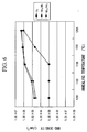
- annealing temperature of the first annealing step (annealing temperature) and BMD density when each of NH 3 /Ar : 2SLM/2SLM and NH 3 /N 2 : 2SLM/2SLM actually flowed as an atmosphere according to the above-described embodiment, is shown in Fig. 6 .
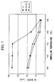
- thermal annealing temperature and DZ width when each of NH 3 /Ar : 2SLM/2SLM and NH 3 /N 2 : 2SLM/2SLM actually flowed as an atmosphere is shown in Fig. 7 .
- N 2 : 4SLM flowed as an atmosphere are further shown in Figs. 6 and 7 .
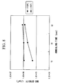
- annealing temperature and BMD density when the annealing temperature in the first thermal annealing step is 1100°C or 1150°C using NH 3 /Ar: 2SLM/2SLM as an atmosphere is shown in Fig. 8 .
- Fig. 8 when the first thermal annealing was carried out for the same thermal annealing time, higher BMD density was obtained at 1150°C which is higher than 1100°C.
- the difference in BMD density between 1100°C and 1150°C gradually increases as thermal annealing time decreases.
- the slip length is shorter when the first thermal annealing is carried out at lower temperature, and when cooling rate is larger. Furthermore, when the atmosphere contains ammonia, it is found that the smaller the amount of ammonia leads to the shorter slip length. This reason is considered that hydrogen (H) having relatively high thermal conductivity decreases, as the amount of ammonia becomes smaller. Therefore, the first thermal annealing is carried out using relatively low flow rate of the atmosphere containing ammonia at relatively low temperature, and cooling is carried out with large cooling rate, generation of slip can be suppressed and satisfactory BMD density can be obtained.
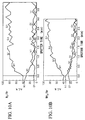
- Fig. 9 shows a slip length from a pin mark when the quartz pin holds the silicon wafer, in order to clearly show the suppressive effect of slip generation by decreasing the thermal annealing temperature in the present invention (NH 3 /Ar).
- the slip length is a value of the maximum interval among dislocation pits measured after 13 ⁇ m is etched off by non-agitated Secco etching.
- slip length is 0.4 mm or less, which is less than that in the conventional method (Ar/N 2 ).
- growth of slip is zero at 1130°C or less, so that slip can be remarkably decreased.
- the thermal annealing step contains nitride gas comprising NH 3 having a lower decomposition temperature than decomposable temperature of N 2 , the nitride gas is decomposed even if lower thermal annealing temperature or shorter thermal annealing time than those in N 2 . Accordingly, since the surface of the silicon wafer is nitrided, vacancies are injected therein and generation of slip is suppressed during the first thermal annealing and subsequently, by carrying out the subsequent second thermal annealing, quality silicon wafers having DZ layers having sufficient thickness and suitably high BMD density therein are obtained. Particularly, the present invention is effective in silicon wafers with 300 mm diameter which are larger than 200 mm diameter wafers.
- the silicon wafer of the present invention has a silicon nitride-oxide film formed by nitriding the surface of the silicon wafer in the first thermal annealing, sufficient amount of vacancies are injected therein and good surface morphology is provided by suppressing surface roughness. Therefore, after the second thermal annealing for oxygen precipitates has been carried out on the silicon wafer, the silicon wafer comprising a BMD layer having high BMD density therein and a DZ layer having satisfactory surface roughness as a surface layer is obtained.
Landscapes
- Engineering & Computer Science (AREA)
- Physics & Mathematics (AREA)
- Condensed Matter Physics & Semiconductors (AREA)
- General Physics & Mathematics (AREA)
- Manufacturing & Machinery (AREA)
- Computer Hardware Design (AREA)
- Microelectronics & Electronic Packaging (AREA)
- Power Engineering (AREA)
- Formation Of Insulating Films (AREA)
- Crystals, And After-Treatments Of Crystals (AREA)
Applications Claiming Priority (7)
| Application Number | Priority Date | Filing Date | Title |
|---|---|---|---|
| JP2000360913 | 2000-11-28 | ||
| JP2000360913 | 2000-11-28 | ||
| JP2001139216 | 2001-05-09 | ||
| JP2001139216 | 2001-05-09 | ||
| JP2001291145 | 2001-09-25 | ||
| JP2001291145A JP4720058B2 (ja) | 2000-11-28 | 2001-09-25 | シリコンウェーハの製造方法 |
| PCT/JP2001/010385 WO2002045149A1 (fr) | 2000-11-28 | 2001-11-28 | Procede de fabrication de tranche de silicium et tranche de silicium |
Publications (3)
| Publication Number | Publication Date |
|---|---|
| EP1345262A1 EP1345262A1 (en) | 2003-09-17 |
| EP1345262A4 EP1345262A4 (en) | 2007-09-05 |
| EP1345262B1 true EP1345262B1 (en) | 2016-04-20 |
Family
ID=27345277
Family Applications (1)
| Application Number | Title | Priority Date | Filing Date |
|---|---|---|---|
| EP01998993.8A Expired - Lifetime EP1345262B1 (en) | 2000-11-28 | 2001-11-28 | Method for producing silicon wafer and silicon wafer |
Country Status (7)
| Country | Link |
|---|---|
| US (2) | US7521381B2 (zh) |
| EP (1) | EP1345262B1 (zh) |
| JP (1) | JP4720058B2 (zh) |
| KR (1) | KR100707728B1 (zh) |
| CN (1) | CN1237585C (zh) |
| TW (1) | TW546741B (zh) |
| WO (1) | WO2002045149A1 (zh) |
Families Citing this family (24)
| Publication number | Priority date | Publication date | Assignee | Title |
|---|---|---|---|---|
| US6503594B2 (en) * | 1997-02-13 | 2003-01-07 | Samsung Electronics Co., Ltd. | Silicon wafers having controlled distribution of defects and slip |
| KR100864117B1 (ko) * | 2001-03-05 | 2008-10-16 | 도쿄엘렉트론가부시키가이샤 | 열처리방법 및 열처리장치 |
| KR100856183B1 (ko) * | 2004-02-16 | 2008-10-10 | 샤프 가부시키가이샤 | 박막 트랜지스터와 그 제조 방법, 표시 장치, 산화막의개질 방법, 산화막의 형성 방법, 반도체 장치, 반도체장치의 제조 방법 및 반도체 장치의 제조 장치 |
| JP4617751B2 (ja) * | 2004-07-22 | 2011-01-26 | 株式会社Sumco | シリコンウェーハおよびその製造方法 |
| JP4711167B2 (ja) * | 2004-08-25 | 2011-06-29 | 信越半導体株式会社 | シリコンエピタキシャルウェーハの製造方法 |
| JP4720164B2 (ja) * | 2004-12-02 | 2011-07-13 | 株式会社Sumco | Soiウェーハの製造方法 |
| JP4743010B2 (ja) * | 2005-08-26 | 2011-08-10 | 株式会社Sumco | シリコンウェーハの表面欠陥評価方法 |
| JP2007194232A (ja) * | 2006-01-17 | 2007-08-02 | Shin Etsu Handotai Co Ltd | シリコン単結晶ウエーハの製造方法 |
| JP4853027B2 (ja) * | 2006-01-17 | 2012-01-11 | 信越半導体株式会社 | シリコン単結晶ウエーハの製造方法 |
| JP2008053521A (ja) | 2006-08-25 | 2008-03-06 | Sumco Techxiv株式会社 | シリコンウェーハの熱処理方法 |
| JP2008294245A (ja) * | 2007-05-25 | 2008-12-04 | Shin Etsu Handotai Co Ltd | エピタキシャルウェーハの製造方法およびエピタキシャルウェーハ |
| JP2010028065A (ja) * | 2008-07-24 | 2010-02-04 | Sumco Corp | シリコンウェーハの製造方法 |
| JP2010109100A (ja) * | 2008-10-29 | 2010-05-13 | Shin Etsu Handotai Co Ltd | シリコンウェーハの製造方法 |
| KR101565794B1 (ko) * | 2008-12-16 | 2015-11-05 | 삼성전자주식회사 | 게더링 효과를 향상시킬 수 있는 실리콘 기판 및 실리콘 웨이퍼, 상기 실리콘 웨이퍼의 열처리 방법 |
| JP5434239B2 (ja) * | 2009-04-30 | 2014-03-05 | 株式会社Sumco | シリコンウェーハの製造方法 |
| KR20120023056A (ko) * | 2009-05-15 | 2012-03-12 | 가부시키가이샤 사무코 | 실리콘 웨이퍼 및 그 제조 방법 |
| JP5583070B2 (ja) * | 2011-04-27 | 2014-09-03 | グローバルウェーハズ・ジャパン株式会社 | シリコンウェーハの熱処理方法 |
| US9945048B2 (en) * | 2012-06-15 | 2018-04-17 | Taiwan Semiconductor Manufacturing Company, Ltd. | Semiconductor structure and method |
| DE102014208815B4 (de) * | 2014-05-09 | 2018-06-21 | Siltronic Ag | Verfahren zur Herstellung einer Halbleiterscheibe aus Silizium |
| JP6100226B2 (ja) * | 2014-11-26 | 2017-03-22 | 信越半導体株式会社 | シリコン単結晶ウェーハの熱処理方法 |
| DE102015200890A1 (de) * | 2015-01-21 | 2016-07-21 | Siltronic Ag | Epitaktisch beschichtete Halbleiterscheibe und Verfahren zur Herstellung einer epitaktisch beschichteten Halbleiterscheibe |
| JP6044660B2 (ja) * | 2015-02-19 | 2016-12-14 | 信越半導体株式会社 | シリコンウェーハの製造方法 |
| JP6822375B2 (ja) * | 2017-10-19 | 2021-01-27 | 信越半導体株式会社 | シリコンエピタキシャルウエーハの製造方法 |
| CN114280072B (zh) * | 2021-12-23 | 2023-06-20 | 宁夏中欣晶圆半导体科技有限公司 | 单晶硅体内bmd的检测方法 |
Family Cites Families (27)
| Publication number | Priority date | Publication date | Assignee | Title |
|---|---|---|---|---|
| US3724215A (en) * | 1971-05-19 | 1973-04-03 | Atomic Energy Commission | Decomposed ammonia radioisotope thruster |
| US4224514A (en) * | 1978-06-16 | 1980-09-23 | Sensor Technology, Inc. | Optical encoder |
| JPS58164229A (ja) * | 1982-03-25 | 1983-09-29 | Sony Corp | 半導体基板処理法 |
| JPS641393A (en) | 1987-06-23 | 1989-01-05 | Victor Co Of Japan Ltd | Voltage control type comb-line filter |
| US5131979A (en) * | 1991-05-21 | 1992-07-21 | Lawrence Technology | Semiconductor EPI on recycled silicon wafers |
| US5665640A (en) * | 1994-06-03 | 1997-09-09 | Sony Corporation | Method for producing titanium-containing thin films by low temperature plasma-enhanced chemical vapor deposition using a rotating susceptor reactor |
| DE19527287C2 (de) * | 1995-07-26 | 2000-06-29 | Heidenhain Gmbh Dr Johannes | Fotoelektrisches Weg- und Winkelmeßsystem zum Messen der Verschiebung zweier Objekte zueinander |
| US6503594B2 (en) * | 1997-02-13 | 2003-01-07 | Samsung Electronics Co., Ltd. | Silicon wafers having controlled distribution of defects and slip |
| US6485807B1 (en) * | 1997-02-13 | 2002-11-26 | Samsung Electronics Co., Ltd. | Silicon wafers having controlled distribution of defects, and methods of preparing the same |
| US5994761A (en) | 1997-02-26 | 1999-11-30 | Memc Electronic Materials Spa | Ideal oxygen precipitating silicon wafers and oxygen out-diffusion-less process therefor |
| EP0993027A4 (en) | 1997-03-28 | 2002-05-29 | Sharp Kk | PROCESS FOR MANUFACTURING SEMICONDUCTOR COMPOUNDS |
| DE69841714D1 (de) | 1997-04-09 | 2010-07-22 | Memc Electronic Materials | Silicium mit niedriger Fehlerdichte und idealem Sauerstoffniederschlag |
| US5780338A (en) * | 1997-04-11 | 1998-07-14 | Vanguard International Semiconductor Corporation | Method for manufacturing crown-shaped capacitors for dynamic random access memory integrated circuits |
| DE19830925A1 (de) * | 1997-08-07 | 1999-02-11 | Heidenhain Gmbh Dr Johannes | Abtasteinheit für eine optische Positionsmeßeinrichtung |
| JPH1192283A (ja) * | 1997-09-18 | 1999-04-06 | Toshiba Corp | シリコンウエハ及びその製造方法 |
| JP3346249B2 (ja) * | 1997-10-30 | 2002-11-18 | 信越半導体株式会社 | シリコンウエーハの熱処理方法及びシリコンウエーハ |
| US6331492B2 (en) * | 1997-12-31 | 2001-12-18 | Texas Instruments Incorporated | Nitridation for split gate multiple voltage devices |
| US6828690B1 (en) * | 1998-08-05 | 2004-12-07 | Memc Electronic Materials, Inc. | Non-uniform minority carrier lifetime distributions in high performance silicon power devices |
| JP2002524845A (ja) * | 1998-09-02 | 2002-08-06 | エムイーエムシー・エレクトロニック・マテリアルズ・インコーポレイテッド | 欠陥密度が低い単結晶シリコンから得られるシリコン・オン・インシュレーター構造体 |
| US6190973B1 (en) * | 1998-12-18 | 2001-02-20 | Zilog Inc. | Method of fabricating a high quality thin oxide |
| EP1175696A2 (de) * | 1999-05-03 | 2002-01-30 | STEAG RTP Systems GmbH | Verfahren zum erzeugen von defekten in einer gitterstruktur eines halbleitermaterials |
| DE10024710A1 (de) | 2000-05-18 | 2001-12-20 | Steag Rtp Systems Gmbh | Einstellung von Defektprofilen in Kristallen oder kristallähnlichen Strukturen |
| JP2001351917A (ja) * | 2000-06-05 | 2001-12-21 | Toshiba Corp | 半導体装置の製造方法及び半導体装置 |
| US6663708B1 (en) * | 2000-09-22 | 2003-12-16 | Mitsubishi Materials Silicon Corporation | Silicon wafer, and manufacturing method and heat treatment method of the same |
| TW473951B (en) * | 2001-01-17 | 2002-01-21 | Siliconware Precision Industries Co Ltd | Non-leaded quad flat image sensor package |
| US20020182342A1 (en) | 2001-04-13 | 2002-12-05 | Luc Ouellet | Optical quality silica films |
| US7273818B2 (en) | 2003-10-20 | 2007-09-25 | Tokyo Electron Limited | Film formation method and apparatus for semiconductor process |
-
2001
- 2001-09-25 JP JP2001291145A patent/JP4720058B2/ja not_active Expired - Lifetime
- 2001-11-12 TW TW090127991A patent/TW546741B/zh not_active IP Right Cessation
- 2001-11-27 KR KR1020010074112A patent/KR100707728B1/ko active IP Right Grant
- 2001-11-28 EP EP01998993.8A patent/EP1345262B1/en not_active Expired - Lifetime
- 2001-11-28 CN CNB011424249A patent/CN1237585C/zh not_active Expired - Fee Related
- 2001-11-28 WO PCT/JP2001/010385 patent/WO2002045149A1/ja active Application Filing
- 2001-11-28 US US10/432,861 patent/US7521381B2/en not_active Expired - Fee Related
-
2005
- 2005-02-09 US US11/053,440 patent/US7670965B2/en not_active Expired - Fee Related
Also Published As
| Publication number | Publication date |
|---|---|
| US7521381B2 (en) | 2009-04-21 |
| JP4720058B2 (ja) | 2011-07-13 |
| KR100707728B1 (ko) | 2007-04-16 |
| US20050130452A1 (en) | 2005-06-16 |
| KR20020041754A (ko) | 2002-06-03 |
| EP1345262A1 (en) | 2003-09-17 |
| US20040053516A1 (en) | 2004-03-18 |
| US7670965B2 (en) | 2010-03-02 |
| JP2003031582A (ja) | 2003-01-31 |
| EP1345262A4 (en) | 2007-09-05 |
| TW546741B (en) | 2003-08-11 |
| CN1356720A (zh) | 2002-07-03 |
| CN1237585C (zh) | 2006-01-18 |
| WO2002045149A1 (fr) | 2002-06-06 |
Similar Documents
| Publication | Publication Date | Title |
|---|---|---|
| US7670965B2 (en) | Production method for silicon wafers and silicon wafer | |
| US7977219B2 (en) | Manufacturing method for silicon wafer | |
| KR100581305B1 (ko) | 저결함 밀도 단결정 실리콘으로부터의 soi 구조체 | |
| US7071080B2 (en) | Process for producing silicon on insulator structure having intrinsic gettering by ion implantation | |
| EP2110466B1 (en) | Silicon single crystal manufacturing method | |
| US6843848B2 (en) | Semiconductor wafer made from silicon and method for producing the semiconductor wafer | |
| EP1909315A1 (en) | Silicon wafer and process for producing the same | |
| KR20010006202A (ko) | 저결함밀도, 이상적 산소침전 실리콘 | |
| KR101684873B1 (ko) | 실리콘 기판의 제조 방법 및 실리콘 기판 | |
| JP2003524874A (ja) | 非酸素析出性のチョクラルスキーシリコンウエハ | |
| US6238478B1 (en) | Silicon single crystal and process for producing single-crystal silicon thin film | |
| JP5062217B2 (ja) | 半導体ウェーハの製造方法 | |
| WO2010131412A1 (ja) | シリコンウェーハおよびその製造方法 | |
| JP3791446B2 (ja) | エピタキシャルウェーハの製造方法及びエピタキシャルウェーハ | |
| JP3778146B2 (ja) | シリコンウェーハの製造方法及びシリコンウェーハ | |
| JP5045710B2 (ja) | シリコンウェーハの製造方法 | |
| JP2009224810A (ja) | シリコンウェーハの製造方法、シリコンウェーハ | |
| JP4345253B2 (ja) | エピタキシャルウェーハの製造方法及びエピタキシャルウェーハ | |
| JP2003100762A (ja) | シリコンウェーハの製造方法及びシリコンウェーハ | |
| WO2004070824A1 (en) | Method for removing crystal originated particles from single-crystal silicon wafer | |
| JP2003077924A (ja) | 半導体ウェーハの製造方法及び半導体ウェーハ | |
| EP1710830A2 (en) | Silicon on insulator structure having intrinsic gettering |
Legal Events
| Date | Code | Title | Description |
|---|---|---|---|
| PUAI | Public reference made under article 153(3) epc to a published international application that has entered the european phase |
Free format text: ORIGINAL CODE: 0009012 |
|
| 17P | Request for examination filed |
Effective date: 20030604 |
|
| AK | Designated contracting states |
Kind code of ref document: A1 Designated state(s): AT BE CH CY DE DK ES FI FR GB GR IE IT LI LU MC NL PT SE TR |
|
| RIN1 | Information on inventor provided before grant (corrected) |
Inventor name: SHIRAKI,HIROYUKI,C/O SUMITOMO MITSUBISHI SIL.CORP Inventor name: NAKADA, YOSHINOBU,C/O SUMITOMO MITUBISHI SIL.CORP |
|
| RBV | Designated contracting states (corrected) |
Designated state(s): DE |
|
| RAP1 | Party data changed (applicant data changed or rights of an application transferred) |
Owner name: SUMCO CORPORATION |
|
| A4 | Supplementary search report drawn up and despatched |
Effective date: 20070802 |
|
| 17Q | First examination report despatched |
Effective date: 20071012 |
|
| APBK | Appeal reference recorded |
Free format text: ORIGINAL CODE: EPIDOSNREFNE |
|
| APBN | Date of receipt of notice of appeal recorded |
Free format text: ORIGINAL CODE: EPIDOSNNOA2E |
|
| APBR | Date of receipt of statement of grounds of appeal recorded |
Free format text: ORIGINAL CODE: EPIDOSNNOA3E |
|
| APAF | Appeal reference modified |
Free format text: ORIGINAL CODE: EPIDOSCREFNE |
|
| APBT | Appeal procedure closed |
Free format text: ORIGINAL CODE: EPIDOSNNOA9E |
|
| GRAP | Despatch of communication of intention to grant a patent |
Free format text: ORIGINAL CODE: EPIDOSNIGR1 |
|
| INTG | Intention to grant announced |
Effective date: 20151109 |
|
| GRAS | Grant fee paid |
Free format text: ORIGINAL CODE: EPIDOSNIGR3 |
|
| GRAA | (expected) grant |
Free format text: ORIGINAL CODE: 0009210 |
|
| RIN1 | Information on inventor provided before grant (corrected) |
Inventor name: SHIRAKI, HIROYUKI Inventor name: NAKADA, YOSHINOBU |
|
| AK | Designated contracting states |
Kind code of ref document: B1 Designated state(s): DE |
|
| REG | Reference to a national code |
Ref country code: DE Ref legal event code: R096 Ref document number: 60149899 Country of ref document: DE |
|
| REG | Reference to a national code |
Ref country code: DE Ref legal event code: R097 Ref document number: 60149899 Country of ref document: DE |
|
| PLBE | No opposition filed within time limit |
Free format text: ORIGINAL CODE: 0009261 |
|
| STAA | Information on the status of an ep patent application or granted ep patent |
Free format text: STATUS: NO OPPOSITION FILED WITHIN TIME LIMIT |
|
| 26N | No opposition filed |
Effective date: 20170123 |
|
| PGFP | Annual fee paid to national office [announced via postgrant information from national office to epo] |
Ref country code: DE Payment date: 20191121 Year of fee payment: 19 |
|
| REG | Reference to a national code |
Ref country code: DE Ref legal event code: R119 Ref document number: 60149899 Country of ref document: DE |
|
| PG25 | Lapsed in a contracting state [announced via postgrant information from national office to epo] |
Ref country code: DE Free format text: LAPSE BECAUSE OF NON-PAYMENT OF DUE FEES Effective date: 20210601 |