EP1243031B9 - Oberflächenmontierbare leuchtdioden-lichtquelle und verfahren zur herstellung einer leuchtdioden-lichtquelle - Google Patents
Oberflächenmontierbare leuchtdioden-lichtquelle und verfahren zur herstellung einer leuchtdioden-lichtquelle Download PDFInfo
- Publication number
- EP1243031B9 EP1243031B9 EP00991779.0A EP00991779A EP1243031B9 EP 1243031 B9 EP1243031 B9 EP 1243031B9 EP 00991779 A EP00991779 A EP 00991779A EP 1243031 B9 EP1243031 B9 EP 1243031B9
- Authority
- EP
- European Patent Office
- Prior art keywords
- molding composition
- light source
- light
- emitting diode
- conversion substance
- Prior art date
- Legal status (The legal status is an assumption and is not a legal conclusion. Google has not performed a legal analysis and makes no representation as to the accuracy of the status listed.)
- Expired - Lifetime
Links
Images
Classifications
-
- H—ELECTRICITY
- H10—SEMICONDUCTOR DEVICES; ELECTRIC SOLID-STATE DEVICES NOT OTHERWISE PROVIDED FOR
- H10H—INORGANIC LIGHT-EMITTING SEMICONDUCTOR DEVICES HAVING POTENTIAL BARRIERS
- H10H20/00—Individual inorganic light-emitting semiconductor devices having potential barriers, e.g. light-emitting diodes [LED]
- H10H20/80—Constructional details
- H10H20/85—Packages
- H10H20/8506—Containers
-
- H—ELECTRICITY
- H10—SEMICONDUCTOR DEVICES; ELECTRIC SOLID-STATE DEVICES NOT OTHERWISE PROVIDED FOR
- H10H—INORGANIC LIGHT-EMITTING SEMICONDUCTOR DEVICES HAVING POTENTIAL BARRIERS
- H10H20/00—Individual inorganic light-emitting semiconductor devices having potential barriers, e.g. light-emitting diodes [LED]
- H10H20/80—Constructional details
- H10H20/85—Packages
- H10H20/851—Wavelength conversion means
- H10H20/8511—Wavelength conversion means characterised by their material, e.g. binder
-
- H—ELECTRICITY
- H10—SEMICONDUCTOR DEVICES; ELECTRIC SOLID-STATE DEVICES NOT OTHERWISE PROVIDED FOR
- H10W—GENERIC PACKAGES, INTERCONNECTIONS, CONNECTORS OR OTHER CONSTRUCTIONAL DETAILS OF DEVICES COVERED BY CLASS H10
- H10W72/00—Interconnections or connectors in packages
- H10W72/50—Bond wires
- H10W72/531—Shapes of wire connectors
- H10W72/536—Shapes of wire connectors the connected ends being ball-shaped
-
- H—ELECTRICITY
- H10—SEMICONDUCTOR DEVICES; ELECTRIC SOLID-STATE DEVICES NOT OTHERWISE PROVIDED FOR
- H10W—GENERIC PACKAGES, INTERCONNECTIONS, CONNECTORS OR OTHER CONSTRUCTIONAL DETAILS OF DEVICES COVERED BY CLASS H10
- H10W72/00—Interconnections or connectors in packages
- H10W72/50—Bond wires
- H10W72/531—Shapes of wire connectors
- H10W72/5363—Shapes of wire connectors the connected ends being wedge-shaped
-
- H—ELECTRICITY
- H10—SEMICONDUCTOR DEVICES; ELECTRIC SOLID-STATE DEVICES NOT OTHERWISE PROVIDED FOR
- H10W—GENERIC PACKAGES, INTERCONNECTIONS, CONNECTORS OR OTHER CONSTRUCTIONAL DETAILS OF DEVICES COVERED BY CLASS H10
- H10W72/00—Interconnections or connectors in packages
- H10W72/851—Dispositions of multiple connectors or interconnections
- H10W72/874—On different surfaces
- H10W72/884—Die-attach connectors and bond wires
-
- H—ELECTRICITY
- H10—SEMICONDUCTOR DEVICES; ELECTRIC SOLID-STATE DEVICES NOT OTHERWISE PROVIDED FOR
- H10W—GENERIC PACKAGES, INTERCONNECTIONS, CONNECTORS OR OTHER CONSTRUCTIONAL DETAILS OF DEVICES COVERED BY CLASS H10
- H10W74/00—Encapsulations, e.g. protective coatings
-
- H—ELECTRICITY
- H10—SEMICONDUCTOR DEVICES; ELECTRIC SOLID-STATE DEVICES NOT OTHERWISE PROVIDED FOR
- H10W—GENERIC PACKAGES, INTERCONNECTIONS, CONNECTORS OR OTHER CONSTRUCTIONAL DETAILS OF DEVICES COVERED BY CLASS H10
- H10W90/00—Package configurations
- H10W90/701—Package configurations characterised by the relative positions of pads or connectors relative to package parts
- H10W90/751—Package configurations characterised by the relative positions of pads or connectors relative to package parts of bond wires
- H10W90/756—Package configurations characterised by the relative positions of pads or connectors relative to package parts of bond wires between a chip and a stacked lead frame, conducting package substrate or heat sink
Definitions
- the invention relates to a surface-mountable light-emitting diode light source according to the preamble of patent claim 1.
- the publication JP-A 5 037 008 describes a device for optical coupling.
- the invention further relates to a method for producing a light source based on a semiconductor light emitting diode (hereinafter referred to as semiconductor LED), in particular a surface mountable semiconductor LED, according to the preamble of claim 9. It relates in particular a semiconductor LED Mixed light source, in particular a white light source.
- semiconductor LED semiconductor light emitting diode
- a semiconductor LED Mixed light source in particular a white light source.
- a semiconductor LED having an emission spectrum in the ultraviolet or blue spectral range is used and the semiconductor LED is surrounded at its light exit sides by a molding compound containing a conversion substance through which the light spectrum emitted by the semiconductor LED at least partially is converted into light of other wavelengths, so that the visual impression of a white light source is formed, that is, that the light source emits white light in total.
- a surface mountable LED device with projecting from the housing Lötanschluß kind is in the WO 98/12757 described.
- the Lötanschlußst a leadframe starting from the chip mounting surface in a straight line in the plane of the mounting surface of a plastic housing led out and outside the plastic housing to the component mounting side bent S-shaped, so that arise after the S-bend solder pads. With the solder pads, the device can be mounted on a printed circuit board.
- a wavelength-converting potting compound for an electroluminescent device is described with an ultraviolet, blue, or green light emitting body based on a transparent epoxy resin, which is mixed with a phosphor, in particular with an inorganic phosphor pigment powder with phosphor pigments from the group of phosphors.
- a white light source is described, in which a radiation-emitting semiconductor LED based on GaAlN with an emission maximum between 420 nm and 460 nm is used together with a phosphor which is chosen so that a of the semiconductor body emitted blue radiation in complementary wavelength ranges, in particular blue and yellow, or to additive color triplets, eg blue, green and red, is converted.
- the yellow or the green and the red light is generated by the phosphors.
- the hue (color location in the CIE chromaticity diagram) of the white light thus produced can be varied by suitable choice of the luminescent material (s) with regard to mixing and concentration.
- the WO 98/54929 a visible light-emitting semiconductor device with a UV / blue LED, which is arranged in a recess of a carrier body whose surface has a light-reflecting layer and is filled with a transparent material which surrounds the LED at their light exit sides.
- the transparent material has a refractive index lower than the refractive index of the light-active region of the LED.
- JP-10093146 A a radial LED device is described in which is incorporated to improve the radiation intensity and brightness in the plastic housing casting a phosphor which is excited by the radiation of the semiconductor LED chip and emits at a longer wavelength.
- a radial LED design is also in the US Pat. No. 5,777,433 described.
- nanoparticles which have a greater refractive index than the transparent potting material are incorporated into the radial plastic encapsulation, which consists, for example, of epoxy or another suitable transparent organic potting material, for increasing the refractive index of the plastic material.
- a white light source based on a semiconductor LED is known.
- an arrangement with an electroluminescent or laser diode in which the emission spectrum emitted by the diode is shifted toward greater wavelengths by means of an element made of plastic, which is mixed with a phosphorescent, light-converting organic dye.
- the light emitted by the arrangement has a different color than the light emitted by the light-emitting diode.
- light-emitting diode arrangements which shine in different colors can be produced with one and the same type of light-emitting diode.
- a pre-hosed component is produced in that a prefabricated lead frame (leadframe) is encapsulated with a suitable plastic material which forms the housing of the component.
- This component has at the top of a recess into which leadframe connections are inserted from two opposite sides, on one of which a semiconductor LED is adhesively bonded and electrically contacted.
- the phosphor potting compound usually a transparent epoxy resin, filled.
- the present invention is in particular the object to provide a surface mountable light-emitting diode light source available, which has a small footprint. Furthermore, a method for producing a light source, in particular a surface mountable light source based on a semiconductor LED is to be specified, which manages with a smaller number of manufacturing steps, which has improved properties with respect to temperature resistance in use over the known arrangements. In particular, it is intended to specify the production of a mixed-color LED light source, in particular a white light source.
- the first object is achieved by a surface-mountable light-emitting diode light source having the features of patent claim 1.
- each of the leadframe connections within the transparent plastic molded body has an S-shaped bend, through which it is led from a chip mounting region to a mounting side of the light-emitting diode light source.
- the leadframe connections are thus already led out in the mounting plane of the plastic housing or molded body. Consequently, the undersides of the leadframe connections already lead out of the plane of the underside of the plastic molded body and no longer have any bending outside, which on the one hand causes increased space requirements and on the other hand causes mechanical stress on the plastic molded body during the bending process. The latter involves the risk of delamination between the plastic molded body and the leadframe, which usually leads to a reduced moisture stability.
- Preferred embodiments of the surface-mountable light-emitting diode light source are the subject of the dependent claims 2 to 8.
- the second object is achieved by a method having the features of claim 9.
- the method is particularly preferably used for producing a white light source based on a semiconductor LED, which emits light radiation in the ultraviolet or blue spectral range, in which method the LED is mounted on a leadframe and electrically contacted, a transparent plastic molding compound mixed with a conversion substance is, and the leadframe is preferably formed in the transfer molding process with the molding compound such that the LED is surrounded at its light exit sides of the molding compound.
- the inventive method thus dispenses with the formation of a depression and the use of two different materials and instead provides for the use of a single transparent plastic molding compound, which is first mixed with the conversion substance and then molded around the lead frame, preferably injected.
- the cured molding compound thus serves at the same time as a component housing as well as a transparent conversion substance matrix.
- the production process is considerably simplified, since in a single molding process, in particular a transfer molding process, both the housing and the conversion substance are formed provided.
- a device is produced, which has improved stability properties, since the problem of adhesion between two materials, which may also have different coefficients of thermal expansion, no longer occurs.
- the sedimentation behavior of the inorganic phosphors during the production, storage and processing of the converter resins is decisively improved.
- the x, y color locations of the white light sources are subject to only slight fluctuations and the illumination of the light-emitting diodes is improved.
- Prolonged dispersing of the phosphor for agglomerate-free converter casting resins and for setting stable viscosities even during the casting resin storage eliminates the same as a complex packaging in the form of syringes.
- transparent molding compounds are mixed together, for example as tablets or as granules, together with the phosphor by grinding and optionally sieving. Sedimentation of the phosphor in the production and storage can thus be largely prevented.
- the plastic molding compound may be a commercially available molding compound as a starting material and consists essentially of an epoxy cresol novolak or epoxy resin systems with an anhydride or a phenolic curing system, for example.
- the conversion substance may be an inorganic phosphor pigment powder with phosphor pigments from the group of phosphors with the general formula A 3 B 5 X 12 : M, which are dispersed in the plastic molding compound.
- particles from the group of the Ce-doped garnets can be used as the phosphor pigments, with particular mention being made of Ce-doped yttrium aluminum garnet (Y 3 Al 5 O 12 : Ce).
- Other conceivable conversion substances are sulfide- and oxysulfide-based host lattices, aluminates, borates, etc., with correspondingly short-wavelength excitable metal centers. Also organometallic phosphor systems are to be considered.
- the phosphor can also be formed by soluble and sparingly soluble organic dyes and phosphor blends.
- adhesion promoter preferably in pre-dried conversion substance, can preferably be mixed in liquid form in order to improve the adhesion of the conversion substance to the plastic molding compound.
- adhesion promoters may be 3-glycidoxypropyltrimethoxysilane or further trialkoxysilane-based derivatives.
- a mold release or release agent can be added.
- Such mold release agents facilitate the dissolution of the cured molding compound from the mold.
- a wax-based solid release agent or a metal soap with long-chain carboxylic acids, in particular stearates, can be used.
- fillers for example, inorganic fillers can be added, by which the refractive index of the molding compound can be increased, whereby the light output of the white light source can be increased.
- inorganic fillers for example, TiO 2 , ZrO 2 , ⁇ -Al 2 O 3 , etc. can be used.
- the conversion substance and optionally the further fillers are mixed by first being roughly mixed and then the mixture is ground in a mill, whereby a very fine, homogeneous powder is obtained.
- the method can be carried out in such a way that a surface-mountable component is produced.
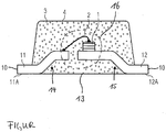
- an embodiment of a white light source according to the invention is shown in a cross section along a longitudinal axis of a lead frame.
- two leadframe terminals 11 and 12 are formed, which are initially held together in a conventional manner by narrow connecting webs, but in the course of a generally multi-stage plastic extrusion by separating the connecting webs are isolated from each other.
- a finished-processed semiconductor LED 1 with an electrically conductive connection means such as conductive silver or the like is glued on the inside end portion, so that the n- or p-side of the semiconductor LED 1 is connected to the leadframe terminal 12.
- the opposite n- or p-type contact side is connected by a bonding wire 2 to the end portion of the other leadframe terminal 11.
- the leadframe 10, on which the LED chip 1 is mounted in a chip mounting region 16, is formed with a transparent plastic molding compound 3, from which a leadframe connection 11, 12 each protrudes on two opposite side surfaces.
- each of the leadframe terminals 11, 12 has an S-like bend 14, 15 from a chip mounting area 16 to a mounting side 13 of the light-emitting diode light source.
- a plastic molding compound used 3 resin-based consists essentially of a pre-reacted epoxy resin, in particular a Epoxynovolak or Epoxykresolnovolak consists.
- the epoxy resin is in particular pre-reacted with a phenolic and / or anhydride curing agent.
- the plastic molding compound is added to a mold release or release agent.
- the mold release agent is, for example, a solid wax-based mold release agent or a metal soap with long-chain carboxylic acids, in particular stearates.
- the plastic molding compound may be added to increase the refractive index of at least one inorganic filler such as TiO 2 , ZrO 2 or ⁇ -Al 2 O 3 .
- the LED chip 1 is mounted in the chip mounting region 16 on the leadframe 10 and electrically conductively connected to the leadframe terminals 11,12.
- the lead frame terminals 11, 12 are provided with S-like bends 14, 15 before or after the mounting of the semiconductor LED chip 1.
- the semiconductor LED chip 1 including the S-type bends 14,15 of the leadframe 10 are preferably formed by pressing with a transparent plastic molding compound 3.
- the semiconductor LED 1 has an emission spectrum which is in the ultraviolet or blue spectral range.
- the semiconductor LED 1 is constructed on the basis of GaN or InGaN.
- it can alternatively also consist of the material system ZnS / ZnSe or of another material system suitable for this spectral range.
- a transparent plastic molding compound 3 is injected onto the leadframe connections 11 and 12 in a suitable injection-compression molding apparatus.
- Embedded phosphor particles 4 consist of a conversion substance, with which an at least partial wavelength conversion of the light emitted from the semiconductor LED light radiation 1 is brought about. By this wavelength conversion, an emission spectrum is generated, which causes the visual impression of a white light source.
- the prefabrication of the lead frame 10 and the encapsulation by the consisting of the plastic molding compound 3, optionally the phosphor particles 4 and optionally other fillers molding compound is such that the lead frame sections 11 and 12 are led out horizontally from the molding compound, in such a way that their solder Pads 11A and 12A are substantially in the same plane as the back 13 of the potting, which is usually the bearing surface of the device on a circuit board.
- the leadframe connections 11 and 12 are already bent to the final shape before the encapsulation.
- the finished component can advantageously be soldered to the planar horizontal pads 11A and 12A on a printed circuit board (board) in the reflow process.
- a suitable for the SMT (Surface Mounting Technology) assembly component is produced.
- the production of the by the plastic molding compound 3, the phosphor particles 4 and optionally further fillers formed molding material constitutes an essential element of the present invention.
- the phosphor an inorganic phosphor pigment powder with phosphor pigments from the group of phosphors having the general formula A 3 B 5 X 12 : M can be used, wherein especially the group of the Ce-doped grenade is to call.
- particles of the fluorescent pigment YAG: Ce are characterized by particular conversion efficiency.
- This conversion substance is known under the product name L175 from Osram. An attempt was made with this conversion substance to be mixed with a molding compound, using a Nitto NT-300 H10.000 molding compound with internal mold release agent. As a test preparation, the conversion substance L175 was pre-dried at 200 ° C for about 8h.
- a surface modifier named diethylene glycol monomethyl ether in liquid form was added to the predried converter (0.1% by weight based on weight of the molding compound).
- This mixture was sealed airtight in a glass jar and allowed to stand overnight.
- the conversion substance was added to the molding compound of the above type.
- the molding compound had previously been ground in powder form in a mill (for example ball mill).
- the mixing ratio was 20% by weight of conversion substance / DEGME mixture and 80% by weight of Nitto NT 300H-10,000. After roughly mixing the mixture by stirring, the mixture was again mixed in a mill (for example ball mill) and ground, thus producing very fine powder.
- adhesion promoter such as 3-glycidoxypropyltrimethoxysilane, for example with the product name A-187 from Huls AG.
- This adhesion promoter can be added directly after the drying process to the phosphor in concentrations up to 3% by weight and mixed overnight at room temperature.
- the inventive method has been described according to embodiment of an SMD (surface mounted design) - design, but it can also be realized in a so-called radial diode.
- the method of the invention may also be used to produce a lateral direction, i. be applied with a main emission parallel to the plane of the board emitting LED device.
Landscapes
- Led Device Packages (AREA)
Applications Claiming Priority (3)
| Application Number | Priority Date | Filing Date | Title |
|---|---|---|---|
| DE19963806A DE19963806C2 (de) | 1999-12-30 | 1999-12-30 | Verfahren zum Herstellen einer Leuchtdioden-Weißlichtquelle, Verwendung einer Kunststoff-Preßmasse zum Herstellen einer Leuchtioden-Weißlichtquelle und oberflächenmontierbare Leuchtdioden-Weißlichtquelle |
| DE19963806 | 1999-12-30 | ||
| PCT/DE2000/004660 WO2001050540A1 (de) | 1999-12-30 | 2000-12-28 | Oberflächenmontierbare leuchtdioden-lichtquelle und verfahren zur herstellung einer leuchtdioden-lichtquelle |
Publications (3)
| Publication Number | Publication Date |
|---|---|
| EP1243031A1 EP1243031A1 (de) | 2002-09-25 |
| EP1243031B1 EP1243031B1 (de) | 2017-03-08 |
| EP1243031B9 true EP1243031B9 (de) | 2017-07-26 |
Family
ID=7935014
Family Applications (1)
| Application Number | Title | Priority Date | Filing Date |
|---|---|---|---|
| EP00991779.0A Expired - Lifetime EP1243031B9 (de) | 1999-12-30 | 2000-12-28 | Oberflächenmontierbare leuchtdioden-lichtquelle und verfahren zur herstellung einer leuchtdioden-lichtquelle |
Country Status (6)
| Country | Link |
|---|---|
| US (2) | US7098588B2 (enExample) |
| EP (1) | EP1243031B9 (enExample) |
| JP (2) | JP2003519929A (enExample) |
| CN (1) | CN100375299C (enExample) |
| DE (2) | DE19964252A1 (enExample) |
| WO (1) | WO2001050540A1 (enExample) |
Families Citing this family (102)
| Publication number | Priority date | Publication date | Assignee | Title |
|---|---|---|---|---|
| AUPR570501A0 (en) * | 2001-06-15 | 2001-07-12 | Q1 (Pacific) Limited | Led lamp |
| AUPQ818100A0 (en) | 2000-06-15 | 2000-07-06 | Arlec Australia Limited | Led lamp |
| US7320632B2 (en) | 2000-06-15 | 2008-01-22 | Lednium Pty Limited | Method of producing a lamp |
| DE10131698A1 (de) * | 2001-06-29 | 2003-01-30 | Osram Opto Semiconductors Gmbh | Oberflächenmontierbares strahlungsemittierendes Bauelement und Verfahren zu dessen Herstellung |
| DE10134968A1 (de) * | 2001-07-23 | 2003-02-20 | Lite On Electronics Inc | Leuchtdiode und Verfahren zu deren Herstellung |
| DE10147986A1 (de) * | 2001-09-28 | 2003-04-10 | Osram Opto Semiconductors Gmbh | Oberflächenmontierbare Leuchtdioden-Lichtquelle und Verfahren zur Herstellung derselben |
| DE10153615C1 (de) * | 2001-10-31 | 2003-07-24 | Osram Opto Semiconductors Gmbh | Verfahren zur Herstellung von elektronischen Bauteilen |
| DE10213294B4 (de) | 2002-03-25 | 2015-05-13 | Osram Gmbh | Verwendung eines UV-beständigen Polymers in der Optoelektronik sowie im Außenanwendungsbereich, UV-beständiges Polymer sowie optisches Bauelement |
| DE10214208B9 (de) * | 2002-03-28 | 2006-12-28 | Osram Opto Semiconductors Gmbh | Gußform für ein elektronisches Bauelement und elektronisches Bauelement |
| US6870311B2 (en) * | 2002-06-07 | 2005-03-22 | Lumileds Lighting U.S., Llc | Light-emitting devices utilizing nanoparticles |
| US6841802B2 (en) | 2002-06-26 | 2005-01-11 | Oriol, Inc. | Thin film light emitting diode |
| US20040124433A1 (en) * | 2002-07-19 | 2004-07-01 | Kelly Stephen G. | Process for fabricating, and light emitting device resulting from, a homogenously mixed powder/pelletized compound |
| DE10234978A1 (de) * | 2002-07-31 | 2004-02-12 | Osram Opto Semiconductors Gmbh | Oberflächenmontierbares Halbleiterbauelement und Verfahren zu dessen Herstellung |
| WO2004017407A1 (de) | 2002-07-31 | 2004-02-26 | Osram Opto Semiconductors Gmbh | Oberflächenmontierbares halbleiterbauelement und verfahren zu dessen herstellung |
| US20050047115A1 (en) * | 2002-09-17 | 2005-03-03 | Hsi-Huang Lin | Method for making a lamp string |
| US6879040B2 (en) * | 2002-09-18 | 2005-04-12 | Agilent Technologies, Inc. | Surface mountable electronic device |
| DE10250877B4 (de) * | 2002-10-31 | 2008-09-04 | Osram Opto Semiconductors Gmbh | Lichtemittierendes Halbleiterbauelement, Herstellungsverfahren und Verwendung dafür, eine Vielzahl der lichtemittierenden Halbleiterbauelemente enthaltendes Modul und dessen Verwendung |
| DE10258193B4 (de) | 2002-12-12 | 2014-04-10 | Osram Opto Semiconductors Gmbh | Verfahren zum Herstellen von Leuchtdioden-Lichtquellen mit Lumineszenz-Konversionselement |
| DE10261672B4 (de) * | 2002-12-31 | 2005-11-24 | Osram Opto Semiconductors Gmbh | LED-Chip mit Konversionsstoff, optoelektronisches Bauelement mit einem derartigen LED-Chip und Verfahren zum Herstellen eines derartigen LED-Chips |
| DE10303455B4 (de) * | 2003-01-29 | 2007-11-29 | Osram Opto Semiconductors Gmbh | Leiterrahmenband und Verfahren zum Herstellen einer Mehrzahl von Leiterrahmen-basierten Leuchtdiodenbauelementen |
| KR20040092512A (ko) * | 2003-04-24 | 2004-11-04 | (주)그래픽테크노재팬 | 방열 기능을 갖는 반사판이 구비된 반도체 발광장치 |
| US7604378B2 (en) | 2003-07-02 | 2009-10-20 | S.C. Johnson & Son, Inc. | Color changing outdoor lights with active ingredient and sound emission |
| US7520635B2 (en) | 2003-07-02 | 2009-04-21 | S.C. Johnson & Son, Inc. | Structures for color changing light devices |
| US7484860B2 (en) | 2003-07-02 | 2009-02-03 | S.C. Johnson & Son, Inc. | Combination white light and colored LED light device with active ingredient emission |
| US7318659B2 (en) * | 2004-03-03 | 2008-01-15 | S. C. Johnson & Son, Inc. | Combination white light and colored LED light device with active ingredient emission |
| US7476002B2 (en) | 2003-07-02 | 2009-01-13 | S.C. Johnson & Son, Inc. | Color changing light devices with active ingredient and sound emission for mood enhancement |
| US7915085B2 (en) * | 2003-09-18 | 2011-03-29 | Cree, Inc. | Molded chip fabrication method |
| US7965031B2 (en) | 2003-09-24 | 2011-06-21 | Osram Gesellschaft mit beschränkter Haftung | White-emitting LED having a defined color temperature |
| JP4457110B2 (ja) | 2003-09-24 | 2010-04-28 | パテント−トロイハント−ゲゼルシヤフト フユール エレクトリツシエ グリユーラムペン ミツト ベシユレンクテル ハフツング | 改善された演色性を有するledをベースとする高効率の照明系 |
| DE10361801A1 (de) * | 2003-12-30 | 2005-08-04 | Osram Opto Semiconductors Gmbh | Strahlungsemittierendes und/oder strahlungsempfangendes Halbleiterbauelement und Verfahren zu dessen Herstellung |
| TWI275189B (en) | 2003-12-30 | 2007-03-01 | Osram Opto Semiconductors Gmbh | Radiation-emitting and/or radiation-receiving semiconductor component and method for producing such component |
| US7503675B2 (en) | 2004-03-03 | 2009-03-17 | S.C. Johnson & Son, Inc. | Combination light device with insect control ingredient emission |
| JP2005310756A (ja) * | 2004-03-26 | 2005-11-04 | Koito Mfg Co Ltd | 光源モジュールおよび車両用前照灯 |
| DE102004038199A1 (de) | 2004-08-05 | 2006-03-16 | Patent-Treuhand-Gesellschaft für elektrische Glühlampen mbH | LED mit niedriger Farbtemperatur |
| DE102004047640A1 (de) | 2004-09-30 | 2006-04-13 | Osram Opto Semiconductors Gmbh | Optoelektronisches Bauelement und Gehäuse für ein optoelektronisches Bauelement |
| JP4757477B2 (ja) * | 2004-11-04 | 2011-08-24 | 株式会社 日立ディスプレイズ | 光源ユニット、それを用いた照明装置及びそれを用いた表示装置 |
| US9070850B2 (en) | 2007-10-31 | 2015-06-30 | Cree, Inc. | Light emitting diode package and method for fabricating same |
| US9793247B2 (en) | 2005-01-10 | 2017-10-17 | Cree, Inc. | Solid state lighting component |
| US7821023B2 (en) | 2005-01-10 | 2010-10-26 | Cree, Inc. | Solid state lighting component |
| US20060186428A1 (en) * | 2005-02-23 | 2006-08-24 | Tan Kheng L | Light emitting device with enhanced encapsulant adhesion using siloxane material and method for fabricating the device |
| DE102005009066A1 (de) * | 2005-02-28 | 2006-09-07 | Osram Opto Semiconductors Gmbh | Verfahren zur Herstellung eines optischen und eines strahlungsemittierenden Bauelementes und optisches sowie strahlungsemittierendes Bauelement |
| US7489073B2 (en) | 2005-04-15 | 2009-02-10 | Patent-Treuhand-Gesellschaft für elektrische Glühlampen mbH | Blue to yellow-orange emitting phosphor, and light source having such a phosphor |
| DE102006016548B9 (de) | 2005-04-15 | 2021-12-16 | Osram Gmbh | Blau bis Gelb-Orange emittierender Leuchtstoff und Lichtquelle mit derartigem Leuchtstoff |
| DE102005036520A1 (de) * | 2005-04-26 | 2006-11-09 | Osram Opto Semiconductors Gmbh | Optisches Bauteil, optoelektronisches Bauelement mit dem Bauteil und dessen Herstellung |
| US7350933B2 (en) * | 2005-05-23 | 2008-04-01 | Avago Technologies Ecbu Ip Pte Ltd | Phosphor converted light source |
| KR100616684B1 (ko) | 2005-06-03 | 2006-08-28 | 삼성전기주식회사 | 고출력 led 패키지 및 그 제조방법 |
| US8669572B2 (en) | 2005-06-10 | 2014-03-11 | Cree, Inc. | Power lamp package |
| JP2007053170A (ja) * | 2005-08-16 | 2007-03-01 | Toshiba Corp | 発光装置 |
| DE102005041064B4 (de) | 2005-08-30 | 2023-01-19 | OSRAM Opto Semiconductors Gesellschaft mit beschränkter Haftung | Oberflächenmontierbares optoelektronisches Bauelement und Verfahren zu dessen Herstellung |
| DE102005059521A1 (de) | 2005-12-13 | 2007-06-14 | Patent-Treuhand-Gesellschaft für elektrische Glühlampen mbH | Rot emittierender Leuchtstoff und Lichtquelle mit einem derartigen Leuchtstoff |
| WO2007081719A2 (en) | 2006-01-05 | 2007-07-19 | Illumitex, Inc. | Separate optical device for directing light from an led |
| US7675145B2 (en) | 2006-03-28 | 2010-03-09 | Cree Hong Kong Limited | Apparatus, system and method for use in mounting electronic elements |
| US8969908B2 (en) | 2006-04-04 | 2015-03-03 | Cree, Inc. | Uniform emission LED package |
| US8748915B2 (en) | 2006-04-24 | 2014-06-10 | Cree Hong Kong Limited | Emitter package with angled or vertical LED |
| US7635915B2 (en) * | 2006-04-26 | 2009-12-22 | Cree Hong Kong Limited | Apparatus and method for use in mounting electronic elements |
| US8735920B2 (en) | 2006-07-31 | 2014-05-27 | Cree, Inc. | Light emitting diode package with optical element |
| US8367945B2 (en) | 2006-08-16 | 2013-02-05 | Cree Huizhou Opto Limited | Apparatus, system and method for use in mounting electronic elements |
| US8087960B2 (en) | 2006-10-02 | 2012-01-03 | Illumitex, Inc. | LED system and method |
| US10295147B2 (en) | 2006-11-09 | 2019-05-21 | Cree, Inc. | LED array and method for fabricating same |
| KR101456266B1 (ko) * | 2006-12-08 | 2014-11-04 | 서울반도체 주식회사 | 발광소자 |
| WO2008073400A1 (en) | 2006-12-11 | 2008-06-19 | The Regents Of The University Of California | Transparent light emitting diodes |
| US7968900B2 (en) * | 2007-01-19 | 2011-06-28 | Cree, Inc. | High performance LED package |
| US9024349B2 (en) | 2007-01-22 | 2015-05-05 | Cree, Inc. | Wafer level phosphor coating method and devices fabricated utilizing method |
| US9711703B2 (en) | 2007-02-12 | 2017-07-18 | Cree Huizhou Opto Limited | Apparatus, system and method for use in mounting electronic elements |
| US7510400B2 (en) * | 2007-03-14 | 2009-03-31 | Visteon Global Technologies, Inc. | LED interconnect spring clip assembly |
| US7621752B2 (en) * | 2007-07-17 | 2009-11-24 | Visteon Global Technologies, Inc. | LED interconnection integrated connector holder package |
| USD615504S1 (en) | 2007-10-31 | 2010-05-11 | Cree, Inc. | Emitter package |
| US8866169B2 (en) | 2007-10-31 | 2014-10-21 | Cree, Inc. | LED package with increased feature sizes |
| US10256385B2 (en) | 2007-10-31 | 2019-04-09 | Cree, Inc. | Light emitting die (LED) packages and related methods |
| US7993940B2 (en) * | 2007-12-05 | 2011-08-09 | Luminus Devices, Inc. | Component attach methods and related device structures |
| USD633631S1 (en) | 2007-12-14 | 2011-03-01 | Cree Hong Kong Limited | Light source of light emitting diode |
| USD634863S1 (en) | 2008-01-10 | 2011-03-22 | Cree Hong Kong Limited | Light source of light emitting diode |
| JP5463447B2 (ja) | 2008-01-18 | 2014-04-09 | 三洋電機株式会社 | 発光装置及びそれを備えた灯具 |
| JP2011512037A (ja) | 2008-02-08 | 2011-04-14 | イルミテックス, インコーポレイテッド | エミッタ層成形のためのシステムおよび方法 |
| US8637883B2 (en) | 2008-03-19 | 2014-01-28 | Cree, Inc. | Low index spacer layer in LED devices |
| US8049230B2 (en) | 2008-05-16 | 2011-11-01 | Cree Huizhou Opto Limited | Apparatus and system for miniature surface mount devices |
| DE102008052751A1 (de) | 2008-10-22 | 2010-04-29 | Osram Opto Semiconductors Gmbh | Verfahren zum Herstellen eines Lumineszenzkonversionselements, Lumineszenzkonversionselement und optoelektronisches Bauteil |
| US8791471B2 (en) | 2008-11-07 | 2014-07-29 | Cree Hong Kong Limited | Multi-chip light emitting diode modules |
| KR20100087851A (ko) * | 2009-01-29 | 2010-08-06 | 삼성전자주식회사 | 발광 유닛, 이의 제조 방법 및 발광 유닛을 포함하는 광원 장치 |
| TW201034256A (en) | 2008-12-11 | 2010-09-16 | Illumitex Inc | Systems and methods for packaging light-emitting diode devices |
| US20110037083A1 (en) * | 2009-01-14 | 2011-02-17 | Alex Chi Keung Chan | Led package with contrasting face |
| US8368112B2 (en) * | 2009-01-14 | 2013-02-05 | Cree Huizhou Opto Limited | Aligned multiple emitter package |
| US8415692B2 (en) | 2009-07-06 | 2013-04-09 | Cree, Inc. | LED packages with scattering particle regions |
| US8598809B2 (en) | 2009-08-19 | 2013-12-03 | Cree, Inc. | White light color changing solid state lighting and methods |
| US8585253B2 (en) | 2009-08-20 | 2013-11-19 | Illumitex, Inc. | System and method for color mixing lens array |
| US8449128B2 (en) | 2009-08-20 | 2013-05-28 | Illumitex, Inc. | System and method for a lens and phosphor layer |
| US20110101062A1 (en) * | 2009-11-04 | 2011-05-05 | Benjamin Franklin Roberts | Pouch and pouches to carry personal items and lights on a belt |
| DE102009058796A1 (de) | 2009-12-18 | 2011-06-22 | OSRAM Opto Semiconductors GmbH, 93055 | Optoelektronisches Bauelement und Verfahren zur Herstellung eines optoelektronischen Bauelements |
| US9166126B2 (en) | 2011-01-31 | 2015-10-20 | Cree, Inc. | Conformally coated light emitting devices and methods for providing the same |
| US8564004B2 (en) | 2011-11-29 | 2013-10-22 | Cree, Inc. | Complex primary optics with intermediate elements |
| US9653656B2 (en) | 2012-03-16 | 2017-05-16 | Advanced Semiconductor Engineering, Inc. | LED packages and related methods |
| US8637887B2 (en) | 2012-05-08 | 2014-01-28 | Advanced Semiconductor Engineering, Inc. | Thermally enhanced semiconductor packages and related methods |
| DE102012106984A1 (de) * | 2012-07-31 | 2014-02-06 | Osram Opto Semiconductors Gmbh | Optoelektronisches Halbleiterbauelement und Verfahren zur Herstellung eines optoelektronischen Halbleiterbauelements |
| DE102012109754A1 (de) * | 2012-10-12 | 2014-04-17 | Osram Opto Semiconductors Gmbh | Optoelektronisches Halbleiterbauelement und Verfahren zum Herstellen eines optoelektronischen Halbleiterbauelements |
| US9059379B2 (en) | 2012-10-29 | 2015-06-16 | Advanced Semiconductor Engineering, Inc. | Light-emitting semiconductor packages and related methods |
| US9618191B2 (en) | 2013-03-07 | 2017-04-11 | Advanced Semiconductor Engineering, Inc. | Light emitting package and LED bulb |
| US9431319B2 (en) * | 2014-08-01 | 2016-08-30 | Linear Technology Corporation | Exposed, solderable heat spreader for integrated circuit packages |
| DE102016104790A1 (de) | 2016-03-15 | 2017-09-21 | Fraunhofer-Gesellschaft zur Förderung der angewandten Forschung e.V. | Materialien für die LED-Verkapselung |
| CN108540086A (zh) * | 2018-01-18 | 2018-09-14 | 浙江人和光伏科技有限公司 | 一种太阳能电池接线盒的导电模块 |
| CN111430343A (zh) * | 2020-03-31 | 2020-07-17 | 深圳市唯亮光电科技有限公司 | 一种垂直式集成封装组件及其封装方法 |
| US11592166B2 (en) | 2020-05-12 | 2023-02-28 | Feit Electric Company, Inc. | Light emitting device having improved illumination and manufacturing flexibility |
| US11876042B2 (en) | 2020-08-03 | 2024-01-16 | Feit Electric Company, Inc. | Omnidirectional flexible light emitting device |
Family Cites Families (32)
| Publication number | Priority date | Publication date | Assignee | Title |
|---|---|---|---|---|
| US3935501A (en) * | 1975-02-13 | 1976-01-27 | Digital Components Corporation | Micro-miniature light source assemblage and mounting means therefor |
| GB1557685A (en) * | 1976-02-02 | 1979-12-12 | Fairchild Camera Instr Co | Optically coupled isolator device |
| US4412135A (en) * | 1979-03-23 | 1983-10-25 | Sharp Kabushiki Kaisha | Photo coupler device molding including filler particles |
| US4287105A (en) * | 1980-01-14 | 1981-09-01 | Plaskon Products, Inc. | Flash resistant epoxy encapsulating composition and process for preparing same |
| US4334035A (en) * | 1981-03-19 | 1982-06-08 | Mitsubishi Petrochemical Co., Ltd. | Unsaturated polyester resin composition |
| JPS596839A (ja) * | 1982-07-05 | 1984-01-13 | Fuji Oil Co Ltd | 大豆乳製品の製造法 |
| JPS596839U (ja) * | 1982-07-07 | 1984-01-17 | 日本電気株式会社 | 半導体装置 |
| JPS60101141A (ja) * | 1983-11-07 | 1985-06-05 | Mitsubishi Electric Corp | エポキシ樹脂用着色剤 |
| JPS6195581A (ja) * | 1984-10-16 | 1986-05-14 | Toshiba Corp | 光結合素子 |
| DE3804293A1 (de) | 1988-02-12 | 1989-08-24 | Philips Patentverwaltung | Anordnung mit einer elektrolumineszenz- oder laserdiode |
| DE3804392A1 (de) * | 1988-02-12 | 1989-08-24 | Basf Ag | Fuellstoffhaltige polyamid-formmassen mit verbesserter oberflaeche und lackierbarkeit |
| JPH02169619A (ja) * | 1988-12-23 | 1990-06-29 | Toshiba Corp | 封止用エポキシ樹脂組成物及びこれを用いてなる光半導体素子 |
| DE4003842C2 (de) * | 1989-02-09 | 1997-06-05 | Shinetsu Chemical Co | Epoxidharzmassen zum Einkapseln von Halbleitern, enthaltend kugelförmiges Siliciumdioxid |
| JPH0537008A (ja) * | 1991-07-29 | 1993-02-12 | Sharp Corp | 光結合装置 |
| JPH05183075A (ja) * | 1991-12-27 | 1993-07-23 | Nitto Denko Corp | 光半導体装置 |
| US5436492A (en) * | 1992-06-23 | 1995-07-25 | Sony Corporation | Charge-coupled device image sensor |
| JP3232698B2 (ja) * | 1992-09-14 | 2001-11-26 | ソニー株式会社 | 樹脂封止型半導体装置とその製造方法 |
| EP0646971B1 (de) | 1993-09-30 | 1997-03-12 | Siemens Aktiengesellschaft | Zweipoliges SMT-Miniatur-Gehäuse für Halbleiterbauelemente und Verfahren zu dessen Herstellung |
| JPH07309927A (ja) * | 1994-05-17 | 1995-11-28 | Nitto Denko Corp | 光半導体装置 |
| DE69525319T2 (de) * | 1994-06-24 | 2002-10-24 | Seiko Epson Corp., Tokio/Tokyo | Durchsichtiges kunststoffmaterial, daraus hergestellte optische gegenstände und herstellungsverfahren |
| JPH08222757A (ja) * | 1995-02-14 | 1996-08-30 | Sharp Corp | 光結合素子 |
| JPH0983013A (ja) * | 1995-09-14 | 1997-03-28 | Sharp Corp | 光結合装置及びその製造方法 |
| DE19604492C1 (de) * | 1996-02-08 | 1997-06-12 | Wustlich Hans Dieter | Spritzgießwerkzeug zur Herstellung von Leuchtdioden |
| US5803579A (en) * | 1996-06-13 | 1998-09-08 | Gentex Corporation | Illuminator assembly incorporating light emitting diodes |
| DE19638667C2 (de) * | 1996-09-20 | 2001-05-17 | Osram Opto Semiconductors Gmbh | Mischfarbiges Licht abstrahlendes Halbleiterbauelement mit Lumineszenzkonversionselement |
| DE29724847U1 (de) | 1996-06-26 | 2004-09-30 | Osram Opto Semiconductors Gmbh | Lichtabstrahlendes Halbleiterbauelement mit Lumineszenzkonversionselement |
| US5777433A (en) * | 1996-07-11 | 1998-07-07 | Hewlett-Packard Company | High refractive index package material and a light emitting device encapsulated with such material |
| US5813753A (en) * | 1997-05-27 | 1998-09-29 | Philips Electronics North America Corporation | UV/blue led-phosphor device with efficient conversion of UV/blues light to visible light |
| FR2765517B1 (fr) * | 1997-07-04 | 1999-08-27 | Oreal | Article en matiere plastique, procede de fabrication et composition de moulage |
| JPH11163419A (ja) * | 1997-11-26 | 1999-06-18 | Rohm Co Ltd | 発光装置 |
| JP3391681B2 (ja) * | 1998-01-26 | 2003-03-31 | 松下電工株式会社 | 光半導体封止用のエポキシ樹脂組成物および樹脂封止型光半導体装置 |
| DE29901093U1 (de) * | 1999-01-22 | 1999-04-08 | Chu Mao Precision Industry Co., Ltd., Shen Kang Hsiang, Taichung | Fotoabtastelement-Leuchtdiode für SMD |
-
1999
- 1999-12-30 DE DE19964252A patent/DE19964252A1/de not_active Ceased
- 1999-12-30 DE DE19963806A patent/DE19963806C2/de not_active Expired - Fee Related
-
2000
- 2000-12-28 EP EP00991779.0A patent/EP1243031B9/de not_active Expired - Lifetime
- 2000-12-28 WO PCT/DE2000/004660 patent/WO2001050540A1/de not_active Ceased
- 2000-12-28 CN CNB008180903A patent/CN100375299C/zh not_active Expired - Fee Related
- 2000-12-28 JP JP2001550820A patent/JP2003519929A/ja active Pending
-
2002
- 2002-07-01 US US10/186,661 patent/US7098588B2/en not_active Expired - Lifetime
-
2006
- 2006-07-10 US US11/456,301 patent/US7534634B2/en not_active Expired - Fee Related
-
2011
- 2011-10-11 JP JP2011223818A patent/JP2012009902A/ja active Pending
Also Published As
| Publication number | Publication date |
|---|---|
| DE19963806C2 (de) | 2002-02-07 |
| US20020195935A1 (en) | 2002-12-26 |
| EP1243031A1 (de) | 2002-09-25 |
| DE19964252A1 (de) | 2002-06-06 |
| EP1243031B1 (de) | 2017-03-08 |
| US20060244000A1 (en) | 2006-11-02 |
| CN1421048A (zh) | 2003-05-28 |
| WO2001050540A1 (de) | 2001-07-12 |
| US7534634B2 (en) | 2009-05-19 |
| JP2012009902A (ja) | 2012-01-12 |
| DE19963806A1 (de) | 2001-07-19 |
| JP2003519929A (ja) | 2003-06-24 |
| US7098588B2 (en) | 2006-08-29 |
| CN100375299C (zh) | 2008-03-12 |
Similar Documents
| Publication | Publication Date | Title |
|---|---|---|
| EP1243031B9 (de) | Oberflächenmontierbare leuchtdioden-lichtquelle und verfahren zur herstellung einer leuchtdioden-lichtquelle | |
| EP1399978B1 (de) | Oberflächenmontierbares strahlungsemittierendes bauelement | |
| EP0862794B1 (de) | Wellenlängenkonvertierende vergussmasse und verfahren zu deren herstellung, verfahren zum herstellen eines licht abstrahlenden halbleiterbauelements und licht abstrahlendes halbleiterbauelement | |
| EP1501909B1 (de) | Wellenlängenkonvertierende reaktionsharzmasse und leuchtdiodenbauelement | |
| EP1441395B9 (de) | Lichtabstrahlendes Halbleiterbauelement mit Lumineszenzkonversionselement | |
| EP1259990B1 (de) | Verfahren zur herstellung eines lichtabstrahlenden halbleiterkörpers mit lumineszenzkonversionselement | |
| EP1897152B1 (de) | Wellenlängenkonvertierendes konvertermaterial, lichtabstrahlendes optisches bauelement und verfahren zu dessen herstellung | |
| EP1277242A1 (de) | Strahlungsemittierendes halbleiterbauelement mit lumineszenzkonversionselement | |
| DE102005009066A1 (de) | Verfahren zur Herstellung eines optischen und eines strahlungsemittierenden Bauelementes und optisches sowie strahlungsemittierendes Bauelement | |
| DE10065381B4 (de) | Strahlungsemittierendes Halbleiterbauelement mit Lumineszenzkonversionselement | |
| EP1700349B1 (de) | Verfahren zum herstellen einer mehrzahl strahlungsemittierender und/oder strahlungsempfangender halbleiterbauelemente | |
| DE202004005228U1 (de) | Strahlungsemittierendes und/oder strahlungsempfangendes Halbleiterbauelement | |
| DE19655185B4 (de) | Mischfarbiges Licht abstrahlendes Halbleiterbauelement mit Lumineszenzkonversionselement | |
| DE10261672B4 (de) | LED-Chip mit Konversionsstoff, optoelektronisches Bauelement mit einem derartigen LED-Chip und Verfahren zum Herstellen eines derartigen LED-Chips |
Legal Events
| Date | Code | Title | Description |
|---|---|---|---|
| PUAI | Public reference made under article 153(3) epc to a published international application that has entered the european phase |
Free format text: ORIGINAL CODE: 0009012 |
|
| 17P | Request for examination filed |
Effective date: 20020620 |
|
| AK | Designated contracting states |
Kind code of ref document: A1 Designated state(s): AT BE CH CY DE DK ES FI FR GB GR IE IT LI LU MC NL PT SE TR |
|
| RBV | Designated contracting states (corrected) |
Designated state(s): AT BE CH DE FR GB LI |
|
| RAP1 | Party data changed (applicant data changed or rights of an application transferred) |
Owner name: OSRAM OPTO SEMICONDUCTORS GMBH |
|
| RAP1 | Party data changed (applicant data changed or rights of an application transferred) |
Owner name: OSRAM OPTO SEMICONDUCTORS GMBH |
|
| 17Q | First examination report despatched |
Effective date: 20080801 |
|
| RIC1 | Information provided on ipc code assigned before grant |
Ipc: H01L 33/48 20100101AFI20160817BHEP Ipc: H01L 33/50 20100101ALN20160817BHEP |
|
| GRAJ | Information related to disapproval of communication of intention to grant by the applicant or resumption of examination proceedings by the epo deleted |
Free format text: ORIGINAL CODE: EPIDOSDIGR1 |
|
| GRAP | Despatch of communication of intention to grant a patent |
Free format text: ORIGINAL CODE: EPIDOSNIGR1 |
|
| REG | Reference to a national code |
Ref country code: DE Ref legal event code: R079 Ref document number: 50016476 Country of ref document: DE Free format text: PREVIOUS MAIN CLASS: H01L0033000000 Ipc: H01L0033480000 |
|
| GRAP | Despatch of communication of intention to grant a patent |
Free format text: ORIGINAL CODE: EPIDOSNIGR1 |
|
| RIC1 | Information provided on ipc code assigned before grant |
Ipc: H01L 33/48 20100101AFI20160915BHEP Ipc: H01L 33/50 20100101ALN20160915BHEP |
|
| RBV | Designated contracting states (corrected) |
Designated state(s): DE FR GB |
|
| RIC1 | Information provided on ipc code assigned before grant |
Ipc: H01L 33/48 20100101AFI20160922BHEP Ipc: H01L 33/50 20100101ALN20160922BHEP |
|
| INTG | Intention to grant announced |
Effective date: 20161006 |
|
| RIC1 | Information provided on ipc code assigned before grant |
Ipc: H01L 33/50 20100101ALN20160926BHEP Ipc: H01L 33/48 20100101AFI20160926BHEP |
|
| GRAS | Grant fee paid |
Free format text: ORIGINAL CODE: EPIDOSNIGR3 |
|
| GRAA | (expected) grant |
Free format text: ORIGINAL CODE: 0009210 |
|
| AK | Designated contracting states |
Kind code of ref document: B1 Designated state(s): DE FR GB |
|
| REG | Reference to a national code |
Ref country code: GB Ref legal event code: FG4D Free format text: NOT ENGLISH |
|
| REG | Reference to a national code |
Ref country code: DE Ref legal event code: R096 Ref document number: 50016476 Country of ref document: DE |
|
| REG | Reference to a national code |
Ref country code: DE Ref legal event code: R097 Ref document number: 50016476 Country of ref document: DE |
|
| PLBE | No opposition filed within time limit |
Free format text: ORIGINAL CODE: 0009261 |
|
| STAA | Information on the status of an ep patent application or granted ep patent |
Free format text: STATUS: NO OPPOSITION FILED WITHIN TIME LIMIT |
|
| PGFP | Annual fee paid to national office [announced via postgrant information from national office to epo] |
Ref country code: DE Payment date: 20171211 Year of fee payment: 18 |
|
| 26N | No opposition filed |
Effective date: 20171211 |
|
| GBPC | Gb: european patent ceased through non-payment of renewal fee |
Effective date: 20171228 |
|
| REG | Reference to a national code |
Ref country code: FR Ref legal event code: ST Effective date: 20180831 |
|
| PG25 | Lapsed in a contracting state [announced via postgrant information from national office to epo] |
Ref country code: FR Free format text: LAPSE BECAUSE OF NON-PAYMENT OF DUE FEES Effective date: 20180102 |
|
| PG25 | Lapsed in a contracting state [announced via postgrant information from national office to epo] |
Ref country code: GB Free format text: LAPSE BECAUSE OF NON-PAYMENT OF DUE FEES Effective date: 20171228 |
|
| REG | Reference to a national code |
Ref country code: DE Ref legal event code: R119 Ref document number: 50016476 Country of ref document: DE |
|
| PG25 | Lapsed in a contracting state [announced via postgrant information from national office to epo] |
Ref country code: DE Free format text: LAPSE BECAUSE OF NON-PAYMENT OF DUE FEES Effective date: 20190702 |