EP1237277A2 - Dispositif semi-conducteur de commutation - Google Patents
Dispositif semi-conducteur de commutation Download PDFInfo
- Publication number
- EP1237277A2 EP1237277A2 EP02004118A EP02004118A EP1237277A2 EP 1237277 A2 EP1237277 A2 EP 1237277A2 EP 02004118 A EP02004118 A EP 02004118A EP 02004118 A EP02004118 A EP 02004118A EP 1237277 A2 EP1237277 A2 EP 1237277A2
- Authority
- EP
- European Patent Office
- Prior art keywords
- terminal pad
- fet2
- transistor
- fet1
- common input
- Prior art date
- Legal status (The legal status is an assumption and is not a legal conclusion. Google has not performed a legal analysis and makes no representation as to the accuracy of the status listed.)
- Withdrawn
Links
Images


Classifications
-
- H—ELECTRICITY
- H03—ELECTRONIC CIRCUITRY
- H03K—PULSE TECHNIQUE
- H03K17/00—Electronic switching or gating, i.e. not by contact-making and –breaking
- H03K17/51—Electronic switching or gating, i.e. not by contact-making and –breaking characterised by the components used
- H03K17/56—Electronic switching or gating, i.e. not by contact-making and –breaking characterised by the components used by the use, as active elements, of semiconductor devices
- H03K17/687—Electronic switching or gating, i.e. not by contact-making and –breaking characterised by the components used by the use, as active elements, of semiconductor devices the devices being field-effect transistors
- H03K17/693—Switching arrangements with several input- or output-terminals, e.g. multiplexers, distributors
-
- H—ELECTRICITY
- H03—ELECTRONIC CIRCUITRY
- H03K—PULSE TECHNIQUE
- H03K17/00—Electronic switching or gating, i.e. not by contact-making and –breaking
- H03K17/51—Electronic switching or gating, i.e. not by contact-making and –breaking characterised by the components used
- H03K17/56—Electronic switching or gating, i.e. not by contact-making and –breaking characterised by the components used by the use, as active elements, of semiconductor devices
- H03K17/687—Electronic switching or gating, i.e. not by contact-making and –breaking characterised by the components used by the use, as active elements, of semiconductor devices the devices being field-effect transistors
-
- H—ELECTRICITY
- H10—SEMICONDUCTOR DEVICES; ELECTRIC SOLID-STATE DEVICES NOT OTHERWISE PROVIDED FOR
- H10D—INORGANIC ELECTRIC SEMICONDUCTOR DEVICES
- H10D84/00—Integrated devices formed in or on semiconductor substrates that comprise only semiconducting layers, e.g. on Si wafers or on GaAs-on-Si wafers
- H10D84/01—Manufacture or treatment
- H10D84/02—Manufacture or treatment characterised by using material-based technologies
- H10D84/05—Manufacture or treatment characterised by using material-based technologies using Group III-V technology
-
- H—ELECTRICITY
- H10—SEMICONDUCTOR DEVICES; ELECTRIC SOLID-STATE DEVICES NOT OTHERWISE PROVIDED FOR
- H10W—GENERIC PACKAGES, INTERCONNECTIONS, CONNECTORS OR OTHER CONSTRUCTIONAL DETAILS OF DEVICES COVERED BY CLASS H10
- H10W20/00—Interconnections in chips, wafers or substrates
- H10W20/40—Interconnections external to wafers or substrates, e.g. back-end-of-line [BEOL] metallisations or vias connecting to gate electrodes
- H10W20/482—Interconnections external to wafers or substrates, e.g. back-end-of-line [BEOL] metallisations or vias connecting to gate electrodes for individual devices provided for in groups H10D8/00 - H10D48/00, e.g. for power transistors
- H10W20/484—Interconnections having extended contours, e.g. pads having mesh shape or interconnections comprising connected parallel stripes
-
- H—ELECTRICITY
- H10—SEMICONDUCTOR DEVICES; ELECTRIC SOLID-STATE DEVICES NOT OTHERWISE PROVIDED FOR
- H10W—GENERIC PACKAGES, INTERCONNECTIONS, CONNECTORS OR OTHER CONSTRUCTIONAL DETAILS OF DEVICES COVERED BY CLASS H10
- H10W70/00—Package substrates; Interposers; Redistribution layers [RDL]
- H10W70/40—Leadframes
- H10W70/411—Chip-supporting parts, e.g. die pads
-
- H—ELECTRICITY
- H03—ELECTRONIC CIRCUITRY
- H03K—PULSE TECHNIQUE
- H03K2217/00—Indexing scheme related to electronic switching or gating, i.e. not by contact-making or -breaking covered by H03K17/00
- H03K2217/0036—Means reducing energy consumption
-
- H—ELECTRICITY
- H10—SEMICONDUCTOR DEVICES; ELECTRIC SOLID-STATE DEVICES NOT OTHERWISE PROVIDED FOR
- H10W—GENERIC PACKAGES, INTERCONNECTIONS, CONNECTORS OR OTHER CONSTRUCTIONAL DETAILS OF DEVICES COVERED BY CLASS H10
- H10W72/00—Interconnections or connectors in packages
- H10W72/071—Connecting or disconnecting
- H10W72/075—Connecting or disconnecting of bond wires
- H10W72/07551—Connecting or disconnecting of bond wires characterised by changes in properties of the bond wires during the connecting
- H10W72/07554—Connecting or disconnecting of bond wires characterised by changes in properties of the bond wires during the connecting changes in dispositions
-
- H—ELECTRICITY
- H10—SEMICONDUCTOR DEVICES; ELECTRIC SOLID-STATE DEVICES NOT OTHERWISE PROVIDED FOR
- H10W—GENERIC PACKAGES, INTERCONNECTIONS, CONNECTORS OR OTHER CONSTRUCTIONAL DETAILS OF DEVICES COVERED BY CLASS H10
- H10W72/00—Interconnections or connectors in packages
- H10W72/50—Bond wires
- H10W72/541—Dispositions of bond wires
- H10W72/5449—Dispositions of bond wires not being orthogonal to a side surface of the chip, e.g. fan-out arrangements
-
- H—ELECTRICITY
- H10—SEMICONDUCTOR DEVICES; ELECTRIC SOLID-STATE DEVICES NOT OTHERWISE PROVIDED FOR
- H10W—GENERIC PACKAGES, INTERCONNECTIONS, CONNECTORS OR OTHER CONSTRUCTIONAL DETAILS OF DEVICES COVERED BY CLASS H10
- H10W72/00—Interconnections or connectors in packages
- H10W72/50—Bond wires
- H10W72/551—Materials of bond wires
-
- H—ELECTRICITY
- H10—SEMICONDUCTOR DEVICES; ELECTRIC SOLID-STATE DEVICES NOT OTHERWISE PROVIDED FOR
- H10W—GENERIC PACKAGES, INTERCONNECTIONS, CONNECTORS OR OTHER CONSTRUCTIONAL DETAILS OF DEVICES COVERED BY CLASS H10
- H10W72/00—Interconnections or connectors in packages
- H10W72/90—Bond pads, in general
- H10W72/931—Shapes of bond pads
- H10W72/932—Plan-view shape, i.e. in top view
-
- H—ELECTRICITY
- H10—SEMICONDUCTOR DEVICES; ELECTRIC SOLID-STATE DEVICES NOT OTHERWISE PROVIDED FOR
- H10W—GENERIC PACKAGES, INTERCONNECTIONS, CONNECTORS OR OTHER CONSTRUCTIONAL DETAILS OF DEVICES COVERED BY CLASS H10
- H10W72/00—Interconnections or connectors in packages
- H10W72/90—Bond pads, in general
- H10W72/951—Materials of bond pads
-
- H—ELECTRICITY
- H10—SEMICONDUCTOR DEVICES; ELECTRIC SOLID-STATE DEVICES NOT OTHERWISE PROVIDED FOR
- H10W—GENERIC PACKAGES, INTERCONNECTIONS, CONNECTORS OR OTHER CONSTRUCTIONAL DETAILS OF DEVICES COVERED BY CLASS H10
- H10W74/00—Encapsulations, e.g. protective coatings
-
- H—ELECTRICITY
- H10—SEMICONDUCTOR DEVICES; ELECTRIC SOLID-STATE DEVICES NOT OTHERWISE PROVIDED FOR
- H10W—GENERIC PACKAGES, INTERCONNECTIONS, CONNECTORS OR OTHER CONSTRUCTIONAL DETAILS OF DEVICES COVERED BY CLASS H10
- H10W90/00—Package configurations
- H10W90/701—Package configurations characterised by the relative positions of pads or connectors relative to package parts
- H10W90/751—Package configurations characterised by the relative positions of pads or connectors relative to package parts of bond wires
- H10W90/754—Package configurations characterised by the relative positions of pads or connectors relative to package parts of bond wires between a chip and a stacked insulating package substrate, interposer or RDL
-
- H—ELECTRICITY
- H10—SEMICONDUCTOR DEVICES; ELECTRIC SOLID-STATE DEVICES NOT OTHERWISE PROVIDED FOR
- H10W—GENERIC PACKAGES, INTERCONNECTIONS, CONNECTORS OR OTHER CONSTRUCTIONAL DETAILS OF DEVICES COVERED BY CLASS H10
- H10W90/00—Package configurations
- H10W90/701—Package configurations characterised by the relative positions of pads or connectors relative to package parts
- H10W90/751—Package configurations characterised by the relative positions of pads or connectors relative to package parts of bond wires
- H10W90/756—Package configurations characterised by the relative positions of pads or connectors relative to package parts of bond wires between a chip and a stacked lead frame, conducting package substrate or heat sink
Definitions
- the invention relates to a semiconductor switching device for switching at high frequencies, especially to a compound semiconductor switching device operating with only one control terminal.
- Mobile communication devices such as mobile telephones often utilize microwaves in the GHz range, and commonly need switching devices for high frequency signals which are used in switching circuits for changing antennas and switching circuits for transmitting and receiving such signals.
- a typical example of such a switching device can be found in Japanese Laid-Open Patent Application No. Hei 9-181642.
- Such a device often uses a field-effect transistor (called FET hereinafter) made on a gallium arsenide (GaAs) substrate, as this material is suitable for use at high frequencies, and developments have been made in forming a monolithic microwave integrated circuit (MMIC) by integrating the aforementioned switching circuits.
- FET field-effect transistor
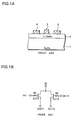
- FIG. 1A is a cross-sectional view of a conventional GaAs metal-semiconductor field-effect transistor (MESFET).
- the GaAs substrate 1 is initially without doping, and has beneath its surface an n-type channel region (or a channel layer) 2 formed by doping with n-type dopants.
- a gate electrode 3 is placed on the surface of the channel region 2, forming a Schottky contact, and a source electrode 4 and a drain electrode 5 are placed on both sides of the gate electrode 3, forming ohmic contacts to the surface of the channel region 2.
- a voltage applied to the gate electrode 3 creates a depletion layer within the channel region 2 beneath the gate electrode 3 and thus controls the channel current between the source electrode 4 and the drain electrode 5.
- FIG. 1B shows the basic circuit configuration of a conventional compound semiconductor switching device called a SPDT (Single Pole Double Throw) switch, using GaAs FETs.
- the source electrode (or the drain electrode) of each FET (FET1 and FET2) is connected to a common input terminal IN.
- the drain electrode (or source electrode) of each FET (FET1 and FET2) is connected to respective output terminals (OUT1 and OUT2).
- the gates of FET1 and FET2 are connected to the control terminals Ctl-1, Ctl-2 through resistors R1, R2, respectively.
- a pair of complementary signals is applied to the two control terminals, Ctl-1, Ctl-2.
- the FET When a high level signal is applied to the control terminal of one of the FETs, the FET changes to an on-state, and a signal fed to the common input terminal IN passes through the FET and reaches one of the output terminals OUT1, OUT2.
- the role of the resistors R1 and R2 is to prevent the leaking of the high frequency signals through the gate electrodes to the DC voltages applied to the control terminals Ctl-1, Ctl-2, which are substantially grounded at high frequency.
- the conventional compound semiconductor switching device described above is configured so that one of the pair of complementary signal is applied to the gate of FET1 via the control terminal Ctl-1 and resistor R1 and other of the pair of complementary signal is applied to the gate of FET2 via the control terminal Ctl-2 and resistor R2. Accordingly, two signals, which forms a complementary signal pair, need to be fed to the two control terminals Ctl-1, Ctl-2.
- Such a configuration needs two external electrodes for the two control terminals Ctl-1, Ctl-2 when the device is housed in a package, resulting in a large package size.
- this design requires additional FETs, resulting higher energy consumption and a larger package size.
- the conventional GaAs MESFET is a depletion type FET and requires the application of a negative voltage for its operation. Therefore, the conventional compound semiconductor switching device described above requires a negative voltage generating circuit for its operation.
- This invention provides a switching circuit device including a common input terminal pad, a first output terminal pad and a second output terminal pad, a first switching element connected to the common input terminal pad and the first output terminal pad, a second switching element connected to the common input terminal pad and the second output terminal pad, a control terminal pad connected to the first switching element and receiving a control signal for the switching device, a first connection connecting the control terminal pad to the second switching element, a second connection connecting the second switching element to a ground, a ground terminal pad for the second connection, a direct current isolation element interrupting a direct current between the second switching element and the common input terminal pad, and a bias element applying a bias voltage to the first switching element.
- the invention also provides a semiconductor switching device including a first field effect transistor and a second field effect transistor, each comprising a source electrode, a gate electrode and a drain electrode which are formed on a channel layer of the respective transistor, a common input terminal pad connected to the source electrode or the drain electrode of the first transistor and connected to the source electrode or the drain electrode of the second transistor, a first output terminal pad connected to the source electrode or the drain electrode of the first transistor which is not connected to the common input terminal pad, a second output terminal pad connected to the source electrode or the drain electrode of the second transistor which is not connected to the common input terminal pad, a control terminal pad connected to the first transistor and the second transistor, a first connection connecting the control terminal pad to the second transistor, a second connection connecting the gate electrode of the second transistor to a ground, a ground terminal pad for the second connection, an direct current isolation element interrupting a direct current between the second transistor and the common input terminal pad, an isolation terminal pad for the external direct current isolation element, and a bias element applying a bias voltage to the first transistor, where
- the invention further provides a semiconductor switching device including a first field effect transistor and a second field effect transistor each comprising a source electrode, a gate electrode and a drain electrode which are formed on a channel layer of the respective transistor, a common input terminal pad connected to the source electrode or the drain electrode of the first transistor and connected to the source electrode or the drain electrode of the second transistor, a first output terminal pad connected to the source electrode or the drain electrode of the first transistor which is not connected to the common input terminal pad, a second output terminal pad connected to the source electrode or the drain electrode of the second transistor which is not connected to the common input terminal pad, a control terminal pad connected to the gate electrode of the first transistor and receiving a control signal for the switching device, a first connection connecting the control terminal pad to the source electrode or the drain electrode of the second transistor, a second connection connecting the gate electrode of the second transistor to a ground, a ground terminal pad for the second connection, a direct current isolation element interrupting a direct current between the second transistor and the common input terminal pad, and a bias element applying a bias voltage
- the invention also provides a circuit device which cooperates with an external direct current isolation element and an external bias element to work as a switch.
- the circuit includes a common input terminal pad, a first output terminal pad and a second output terminal pad, a first switching element connected to the common input terminal pad and the first output terminal pad, a second switching element connected to the common input terminal pad and the second output terminal pad, a control terminal pad connected to the first switching element and receiving a control signal for switching the first transistor and the second transistor, a first connection connecting the control terminal pad to the second switching element, a second connection connecting the second switching element to a ground, a ground terminal pad for the second connection, and an isolation terminal pad connected to the second switching element, wherein the direct current isolation element is connected to the common input terminal pad and the isolation terminal pad, and the bias element is connected to the common input terminal pad or the first output terminal.
- either the direct current isolation element or a resistor of the bias element may be integrated into the circuit device.
- the above embodiments provide SPDT semiconductor switching circuit devices based on GaAs FETs which operate with just one control terminal without employing inverter circuits. Elimination of the external electrodes for the inverter circuits results in a simple package design and small occupancy of printed circuit boards. The energy consumption of this switching device is smaller than a device with inverter circuits.
- Either a predetermined positive voltage or zero voltage is applied to the single control terminal for the switching operation.
- only one power source of positive voltage is required.
- the insertion loss and isolation characteristics are substantially the same as the device with two control terminals.
- ground terminal pad GNDpad and capacitor terminal pad Cpad are required in the embodiments, the increase of chip area due to these additional terminal pads is compensated for by reducing the number of the control terminals to one. Accordingly, the chip size of the embodiments of this invention is substantially the same as the conventional switching device. However, the switching device with one control terminal is very easy to handle when it is assembled into a host device, and thus helps simplifying production process.
- the chip with one control terminal pad Ctlpad can be housed in the same six-pin package as the chip with two control terminal pads.
- the pin for the second control signal is used as the pin for the isolation terminal pad Cpad.
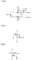
- FIG. 2 is a circuit diagram of a semiconductor switching circuit device of a first embodiment.
- the device has first and second FETs (FET1, FET2), each of which has a source electrode, a gate electrode and a drain electrode on its channel layer.
- the device also has a common input terminal IN connected to the source electrodes (or the drain electrodes) of the FETs (FET1, FET2), a first output terminal connected to the drain electrode (or the source electrode) of the first FET (FET1), a second output terminal connected to the drain electrode (or the source electrode) of the second FET (FET2), and a control terminal Ctl which supplies a control signal to the gate of only FET1.
- the device further includes a bias element applying a predetermined bias to the output terminal OUT1 of FET1 or to the input terminal IN, a direct current isolation element interrupting a direct current between the source electrode (or the drain electrode) of FET2 and the common input terminal IN, a first connection connecting the control terminal Ctl to the drain electrode (or the source electrode) of FET2, and a second connection connecting the gate electrode of FET2 to the ground.
- the two FETs are both GaAs MESFET and integrated into a chip, as described later with reference to FIGS. 7A, 7B and 7C.
- the bias element which includes a power source E and resistor Rc, constantly applies a predetermined positive voltage, for example +3V, to the output terminal OUT1 of the FET1 via resistor Rc.
- the first connection includes resistor Rd, which connects the control terminal Ctl to the drain electrode (or the source electrode) of FET2.
- the second connection includes resistor Rb, which connects gate electrode of FET2 so that the gate is always grounded.
- the isolation element is a capacitor CA, which is inserted between the common input terminal IN and the source electrode (or the drain electrode) of FET2.
- the isolation element isolates FET1 from FET2 in terms of direct current flow. Only one control terminal Ctl applies a control signal to the gate electrode of FET1 via resistor Ra.
- the four resistors Ra, Rb, Rc, Rd prevent leaking of high frequency signals from the gate electrodes and may have identical or different values depending on circuit design.
- FIGS. 3 and 4 show an operational principle of the switching circuit device of FIG. 2.
- a SPDT switching device For a SPDT switching device to operate with a single control terminal configuration, one of the two FETs must turn on while the other turns off under the application of 0 V signal to the single control terminal.
- the term "0 V” refers to a baseline voltage as well known in the art.
- the operation states of the two FETs alternate.
- FIG. 3 corresponds to FET2 of the circuit of FIG. 2.
- the gate voltage is kept constant at 0 V because the gate is grounded via resistor Rb.
- This FET turns on when the voltage applied between its gate and its drain (or source) is equal to the voltage applied between its gate and its source (or drain).
- Vg gate voltage
- Vd drain voltage
- Vs source voltage
- control terminal Ctl is connected to the drain electrode (or the source electrode) of FET2 via resistor Rd, FET2 turns on under an application of 0 voltage to the control terminal Ctl and turns off under an application of a positive voltage, for example +3 V, to the control terminal Ctl.
- FIG. 4 corresponds to FET1 of the circuit of FIG. 2.
- FET1 Under an application of 0 V to the control terminal Ctl, FET1 turns off when a voltage sufficient to turn it off is applied between the gate and the drain as well as between the gate and the source. This is achieved by introducing a bias circuit which constantly applies a bias voltage to the drain (or the source) of FET1.
- FET1 turns on when a voltage equal to the bias voltage is applied to the gate of FET1. Accordingly, FET1 turns off under an application of 0 V to the control terminal Ctl, and turns on under an application of 3 V to the control terminal Ctl.
- circuits of FIGS. 3 and 4 are incorporated into the circuit of FIG. 2 with the capacitor CA isolating the circuit of FIG. 3 from the circuit of FIG. 4 in terms of direct current flow. Interrupting direct current flow between the circuits of FIGS. 3 and 4 prevents interference between the bias conditions of the two circuits.
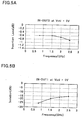
- FIGS. 5A, 5B, 6A and 6B summarize the operational characteristics of a switching device based on the circuit of FIG. 2.
- FIGS. 5A and 5B show the device characteristics when FET2 is on and FET1 is off under an application of 0 V to the control terminal Ctl.
- the insertion loss between the common input terminal IN and the second output terminal OUT2 is shown in FIG. 5A
- the isolation between the common input terminal IN and the first output terminal OUT1 is shown in FIG. 5B. Both the insertion loss and the isolation are appropriate for the switching operation up to 2.5 GHz.
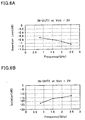
- FIGS. 6A and 6B show the device characteristics when FET2 is off and FET1 is on under an application of 3 V to the control terminal Ctl.
- the insertion loss between the common input terminal IN and the first output terminal OUT1 is shown in FIG. 6A
- the isolation between the common input terminal IN and the second output terminal OUT2 is shown in FIG. 6B. Both the insertion loss and the isolation are appropriate for the switching operation up to 2.5 GHz.
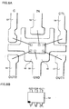
- FIG. 7A is an example of a semiconductor switching device integrated as a compound semiconductor chip, based on the first embodiment of FIG. 2.
- FIG. 7B is a partial cross-sectional view of the chip of FIG. 7A cut along a line connecting points 7A and 7B of FIG. 7A perpendicularly to the channel layer of the FET.
- the two switching FETs (FET1 on the right, FET2 on the left) occupies the central portion of a GaAs substrate.
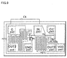
- An isolation terminal pad Cpad for connecting to a direct current isolation element, which is a capacitor CA in this embodiment, the common input terminal pad INpad and the control terminal pad Ctlpad are aligned along the upper edge of the substrate.
- the first and second output terminal pads OUT1pad, OUT2pad and a ground terminal pad GNDpad for grounding FET2 are aligned along the lower edge of the substrate.
- the bias element for FET1 and the capacitor CA are externally connected to the chip as shown in FIG. 7A.
- the capacitor is inserted between the isolation terminal pad Cpad and the common input terminal pad INpad, and the bias element is connected to the first output terminal pad OUT1pad.
- the dashed lines indicate a second layer of wiring which is formed in the same processing step as the gate electrodes of the FET and is made of a gate metal layer (Ti/Pt/Au) 20.
- a third layer of wiring indicated by the solid lines is for connecting the device elements and forming the terminal pads, and is made of a pad metal layer (Ti/Pt/Au) 30.
- a first layer contains an ohmic metal layer (AuGe/Ni/Au) 10 making an ohmic contact with the substrate, which forms the source electrode, the drain electrode and electrodes for the resistors. In FIG. 7A, the first layer is not shown, as it overlaps with the pad metal layer.
- the broken-line rectangles encircling the labels for the terminal pads denote the gate metal layer 20, which is underneath the pad metal layer 30.
- these rectangles approximately correspond to the areas of the pad metal layer 30 to which a bonding wire is attached as described later with reference to FIG. 8A. These areas substantially correspond to the respective terminal pads.
- FIG. 7B shows the placement of the three metal layers 10, 20, 30.
- the GaAs substrate 11 has an n-type channel region 12, and two heavily doped regions at both ends of the channel region 12, namely, a source region 18 and a drain region 19.
- the gate electrode 17, which is made of the gate metal layer 20 as the second metal layer, is formed on the surface of the channel region 12.
- the first layer source electrode 14 and the first layer drain electrode 16, which are made of the ohmic metal layer 10 as the first metal layer, are formed on the surface of the heavily doped regions.
- On top of the first-layer source and drain electrodes 14, 16 is formed the third layer source and drain electrode made of the pad metal layer 30 as the third metal layer, namely the third layer drain electrode 15 and the third layer source electrode 13. This layer is responsible for wiring the device elements of the chip.
- the common input terminal pad INpad is connected to the source electrode (or the drain electrode) of FET1, and is connected to the source electrode (or the drain electrode) of FET2 via a capacitor.
- the drain electrode (or the source electrode) of FET1 is connected to the output terminal pad OUT1pad, and the drain electrode (or the source electrode) of FET2 is connected to the output terminal OUT2pad.
- the control terminal pad Ctlpad is connected to FET1 and FET2 with resistor Rd connecting the control terminal pad Ctlpad to the drain electrode (or the source electrode) of FET2.
- the gate electrode of FET2 is connected the ground terminal pad GNDpad via resistor Rb for grounding.
- the isolation terminal pad Cpad is connected to the source electrode (or the ground electrode) of FET2, and the direct current isolation element, which is a capacitor in this embodiment, is externally connected to the chip using the isolation terminal pad Cpad and the common input terminal INpad.
- the six terminal pads described above occupy significant area of the chip surface, as shown in FIG. 7A.
- Each of the terminal pads needs a predetermined area for wire bonding, and it is not appropriate to reduce the size of the terminal pad for reducing overall chip size. Accordingly, it is required that other device elements including the two FETs and the resistors be arranged in order to save space for chip size reduction.
- the chip of this embodiment has the isolation terminal pad Cpad, the common input terminal pad INpad and the control terminal pad Ctlpad aligned in this order along one edge of the chip, and has first output terminal pad OUT1pad, ground terminal pad GNDpad and the second output terminal pad OUT2 aligned in this order along other edge of the chip.
- a portion of FET2 is formed between the isolation terminal pad Cpad and the second output terminal pad OUT2pad, and a portion of FET1 is formed in the space surrounded by the common input terminal pad INpad, the first output terminal pad OUT1 and the ground terminal pad GNDpad.
- this embodiment provides a switching circuit device with one control terminal pad, or one pin for the control signal when the chip is housed in a package, without increasing overall chip size. Furthermore, in this configuration, FET1 and FET2 are isolated from each other by the ground terminal pad GNDpad. This prevents the leaking of high frequency signal from the common input terminal pad INpad to the output terminal pads OUT1pad, OUT2pad via FET1 and FET2.
- the bias element is, as is the case with the direct current isolation element, externally connected to the chip using the first output terminal pad OUT1.
- the distance between the control terminal pad Ctlpad and the drain electrode (or the source electrode) of FET2 is long.
- Application of conventional wiring design in which the crossing between the wire lines is avoided would increase overall chip size because detouring of wiring line needs additional space. The following measures are taken in this embodiment to avoid overall chip size increase.
- the first is to place the first connection, which is resistor Rd, under the portion of the pad metal layer 30 which extends from the common input pad INpad and connects to the source electrode (or the drain electrode) of FET1.
- the connection runs along the edges of the control terminal pad Ctlpad and the common input terminal pad INpad, which face FET1. Accordingly, the connection between the control terminal pad Ctlpad and the drain electrode (or the source electrode) of FET2 does not need any additional space for its placement because of this intersecting design, and does not contribute to overall chip size increase.
- the second is to place the second connection, which is resistor Rb, in the central portion of the chip.
- This connection which connects the gate electrode of FET2 and the ground terminal pad GNDpad, is bent so that the connection is accommodated in the space surrounded by FET1, FET2 and the ground terminal pad GNDpad.
- This intersecting configuration is achieved by placing a portion of the connection under the portion of the drain electrode (or the source electrode) of FET2 which meets with the resistor Rd above. This is a much better configuration than the conventional configuration in which the connection is detoured around the edge portion of the chip so as to avoid the intersecting wiring configuration.
- FIG. 7C is a pseudo-cross-sectional view cut along the resistor Rb between points 7C and 7B of FIG. 7A.
- FIG. 7C is to describe the structure of the connection for grounding, Rb, under the drain electrode (or the source electrode) of FET2, similar structure applies to the intersection of the first connection, Rd.
- the connection Rb is an n + type high impurity region 40 which is formed on a substrate 11 by an ion injection process at the time of forming source and drain regions on the substrate 11.
- the ohmic metal layer 10, which is the first layer, is formed on the n + type high impurity region 40 at its both ends.
- n + type high impurity region 40 is covered by a nitride film 41.
- the pad metal layer 30, which is the third layer, is formed on top of the ohmic metal layer 10 at the time of forming the drain electrode 18 (or source electrode) of FET2. Accordingly, resistor Rb is insulated from the drain electrode 30 of FET2 by the nitride film 41, resulting in the intersecting configuration.
- FIG. 8A shows an example in which the chip shown in FIG. 7A is mounted on a lead frame for packaging.
- the lead frame with a six-pin configuration has a header 50 located in the middle of the frame on which the compound semiconductor chip 51 is mounted.
- the chip 51 is the same chip shown in FIGS. 7A, 7B and 7C, and the six terminal pads are indicated by the small rectangles on the chip. Although the rectangles are not labeled with any specific name, the configuration of the six terminal pads are the same as that of FIG. 7.
- the three leads 52, 53, 54 on the upper side of the figure are connected by wire bonding to the isolation terminal pad Cpad, the common input terminal pad INpad and the control terminal pad Ctlpad, respectively.
- Three more leads 55, 56, 57 on the bottom side of the figure are connected by wire bonding to the second output terminal pad OUT2pad, ground terminal pad GNDpad and the first output terminal pad OUT1pad, respectively.
- the lead 56 at the bottom center is connected to the header 50.
- the header 50 extends into the space between the leads, i.e. between 52 and 53, between 53 and 54, between 52 and 55, between 54 and 57, and between 55 and 57. This configuration assures the signal separation between the leads.
- the lead 56 connected to the ground terminal pad GNDpad is always grounded, and the lead 54 connected to the control terminal pad Ctlpad is substantially grounded in terms of high frequency signal since only DC signal is applied to the control terminal pad Ctlpad.
- These two leads, or DC pins assures enough separation between the lead 53 forming a common input pin IN and the lead 57 forming a first output pin OUT1, between the lead 53 forming a common input pin IN and the lead 55 forming a second output pin OUT2, and between the lead 57 forming a first output pin OUT1 and the lead 55 forming a second output pin OUT2.
- the chip is covered by a resin layer 58 formed by transfer molding with the six pins C, IN, CTL, OUT2, GND, OUT1 extruding from the packaging, as shown in FIG. 8B.
- This type of packaging is called MCP6, and has a dimension of 2.0 mm x 1.25 mm x 0.9 mm.
- This embodiment is not limited to a lead frame configuration. It is applicable to a lead structure formed on an insulating plate including ceramics and the like using conducting paste and the like. It is also applicable to a lead structure formed on a printed circuit board using copper foils and the like, resulting in a bare chip configuration.
- resistor Rc of the bias element which applies a bias voltage to FET1 may be formed on the chip as well as a bias terminal pad V DD pad for connecting to a power source of the bias element.
- the resistor Rc is connected to the first output terminal pad OUT1pad , it may be connected to the common input terminal pad INpad, as described below with reference to FIGS. 10E and 10F.
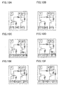
- FIGS. 10A-10F show variations of the first embodiment. These are schematic drawings showing the relative positions on the chip of the terminal pads and the related wirings including the resistors. For simplicity, FETs and resistors are represented by their respective symbols rather than actual two dimensional configurations.
- the chip configuration shown in FIG. 7A is identical to the chip configuration shown in FIG. 10A, and that of FIG. 9 is identical to that of FIG. 10C. All the variations of the first embodiment are effective in overall chip size reduction.
- the chip configuration of FIG. 10A is identical to that of FIG. 7A, and the capacitor CA and the whole bias element including resistor Rc and the power source are externally connected to the chip.
- the connection Rd extending from the control terminal pad Ctlpad connects with FET2 at its source side (or the drain side) which is not connected to the second output terminal pad OUT2pad (FIG. 10B).
- the resistor Rc of the bias element may be integrand into the chip with the option of applying the control signal either on the drain side of FET2 (FIG. 10C) or on the source side (FIG. 10D).
- the resistor Rc may be connected to the common input terminal pad INpad, rather than the first output terminal pad OUT1, with the option of applying the control signal either on the drain side of FET2 (FIG. 10E) or on the source side (FIG. 10F).
- FIG. 11A A second embodiment of this invention is shown in FIG. 11A, in which the direct current isolation element, CA, is integrated into the chip with other device elements being disposed in a configuration similar to the configuration of the first embodiment shown in FIG. 10A.
- This configuration does increase overall chip size for accommodating the capacitor, but has its merit in eliminating the pin C for the isolation element.
- This type of device may be best used when device design allows a larger package size.
- the connection Rd extending from the control terminal pad Ctlpad connects with FET2 at its source side (or the drain side) which is not connected to the second output terminal pad OUT2pad (FIG. 11B).
- the resistor Rc of the bias element may be integrated into the chip with the option of applying the control signal either on the drain side of FET2 (FIG.
- the resistor Rc may be connected to the common input terminal pad INpad, rather than the first output terminal pad OUT1, with the option of applying the control signal either on the drain side of FET2 (FIG. 11E) or on the source side (FIG. 11F).
- connection Rd between the control terminal pad Ctlpad and FET2 is long, the connection is disposed between FET1 and the row of the common input terminal pad INpad and the control terminal pad Ctlpad, and does not require detouring of wiring around the chip edge because of the intersecting structure between the resistor Rd and the metal layer connecting the common input terminal pad INpad and the source electrode of FET1.
- This configuration avoids overall size increase of the device.
- the connection Rb for grounding FET2 is confined to the central area of the chip, further contributing to the chip size reduction. This configuration is also made possible by the intersecting structure between the resistor Rb and a portion of the drain electrode of FET2.
- the leads for the GND pin and the Ctl pin which are substantially grounded in terms of high frequency signals, assures isolation between the lead of IN pin and the lead of the OUT1 pin, between the lead of IN pin and the lead of the OUT2 pin, and between the lead of the OUT1 pin and the lead of the OUT2 pin.
Landscapes
- Junction Field-Effect Transistors (AREA)
- Semiconductor Integrated Circuits (AREA)
- Electronic Switches (AREA)
Applications Claiming Priority (4)
| Application Number | Priority Date | Filing Date | Title |
|---|---|---|---|
| JP2001051862 | 2001-02-27 | ||
| JP2001051863A JP2002261593A (ja) | 2001-02-27 | 2001-02-27 | 化合物半導体スイッチ回路装置 |
| JP2001051862A JP3702190B2 (ja) | 2001-02-27 | 2001-02-27 | 化合物半導体スイッチ回路装置 |
| JP2001051863 | 2001-02-27 |
Publications (2)
| Publication Number | Publication Date |
|---|---|
| EP1237277A2 true EP1237277A2 (fr) | 2002-09-04 |
| EP1237277A3 EP1237277A3 (fr) | 2005-04-27 |
Family
ID=26610159
Family Applications (1)
| Application Number | Title | Priority Date | Filing Date |
|---|---|---|---|
| EP20020004118 Withdrawn EP1237277A3 (fr) | 2001-02-27 | 2002-02-25 | Dispositif semi-conducteur de commutation |
Country Status (5)
| Country | Link |
|---|---|
| US (1) | US6657266B2 (fr) |
| EP (1) | EP1237277A3 (fr) |
| KR (1) | KR20020070120A (fr) |
| CN (1) | CN1236500C (fr) |
| TW (1) | TWI252582B (fr) |
Families Citing this family (21)
| Publication number | Priority date | Publication date | Assignee | Title |
|---|---|---|---|---|
| JP3702189B2 (ja) * | 2001-02-27 | 2005-10-05 | 三洋電機株式会社 | 化合物半導体スイッチ回路装置 |
| JP2003282721A (ja) * | 2002-03-26 | 2003-10-03 | Murata Mfg Co Ltd | 半導体装置および送受信装置 |
| JP2003298305A (ja) * | 2002-03-28 | 2003-10-17 | Fujitsu Quantum Devices Ltd | 高周波スイッチ装置及びこれを用いた電子装置 |
| US6853072B2 (en) * | 2002-04-17 | 2005-02-08 | Sanyo Electric Co., Ltd. | Semiconductor switching circuit device and manufacturing method thereof |
| JP4050096B2 (ja) * | 2002-05-31 | 2008-02-20 | 松下電器産業株式会社 | 高周波スイッチ回路および移動体通信端末装置 |
| JP2005006072A (ja) * | 2003-06-12 | 2005-01-06 | Matsushita Electric Ind Co Ltd | 高周波スイッチ装置および半導体装置 |
| JP4248338B2 (ja) * | 2003-08-05 | 2009-04-02 | パナソニック株式会社 | 半導体装置 |
| JP4559772B2 (ja) * | 2004-05-31 | 2010-10-13 | パナソニック株式会社 | スイッチ回路 |
| KR100548582B1 (ko) * | 2004-07-23 | 2006-02-02 | 주식회사 하이닉스반도체 | 반도체소자의 패드부 |
| JP4810904B2 (ja) | 2005-07-20 | 2011-11-09 | ソニー株式会社 | 高周波スイッチ回路を有する高周波装置 |
| JP4760832B2 (ja) * | 2005-08-09 | 2011-08-31 | 日立金属株式会社 | 高周波スイッチ回路 |
| KR101487738B1 (ko) * | 2007-07-13 | 2015-01-29 | 삼성디스플레이 주식회사 | 액정 표시 장치 및 그의 구동 방법 |
| US8350583B2 (en) | 2009-08-12 | 2013-01-08 | International Business Machines Corporation | Probe-able voltage contrast test structures |
| US8399266B2 (en) | 2011-01-25 | 2013-03-19 | International Business Machines Corporation | Test structure for detection of gap in conductive layer of multilayer gate stack |
| TWI445175B (zh) * | 2011-11-11 | 2014-07-11 | Au Optronics Corp | 主動元件 |
| US9780007B2 (en) | 2012-01-04 | 2017-10-03 | Globalfoundries Inc. | LCR test circuit structure for detecting metal gate defect conditions |
| US9467140B2 (en) | 2014-07-22 | 2016-10-11 | Honeywell International Inc. | Field-effect transistor driver |
| JP6451605B2 (ja) * | 2015-11-18 | 2019-01-16 | 株式会社村田製作所 | 高周波モジュール及び通信装置 |
| WO2018168653A1 (fr) * | 2017-03-14 | 2018-09-20 | 株式会社村田製作所 | Module haute fréquence |
| JP6854985B2 (ja) * | 2018-11-30 | 2021-04-07 | 三菱電機株式会社 | 半導体装置 |
| CN111510089B (zh) * | 2020-04-30 | 2023-08-11 | 中国电子科技集团公司第二十四研究所 | 一种带旁路功能的低噪声放大模块及控制方法 |
Family Cites Families (13)
| Publication number | Priority date | Publication date | Assignee | Title |
|---|---|---|---|---|
| JPS63238716A (ja) * | 1986-11-14 | 1988-10-04 | Nec Corp | スイッチ回路 |
| US5350957A (en) * | 1989-10-20 | 1994-09-27 | Texas Instrument Incorporated | Electronic switch controlled by plural inputs |
| JPH06112795A (ja) * | 1992-07-31 | 1994-04-22 | Hewlett Packard Co <Hp> | 信号切換回路および信号生成回路 |
| JP3169775B2 (ja) * | 1994-08-29 | 2001-05-28 | 株式会社日立製作所 | 半導体回路、スイッチ及びそれを用いた通信機 |
| JP3288209B2 (ja) * | 1994-12-16 | 2002-06-04 | 松下電器産業株式会社 | 半導体集積回路 |
| US5903178A (en) * | 1994-12-16 | 1999-05-11 | Matsushita Electronics Corporation | Semiconductor integrated circuit |
| JPH10247717A (ja) * | 1997-03-04 | 1998-09-14 | Matsushita Electron Corp | 半導体装置 |
| JP2002507074A (ja) * | 1998-03-11 | 2002-03-05 | インフィネオン テクノロジース アクチエンゲゼルシャフト | 移動無線及び移動電話装置のための集積回路 |
| JP2000049341A (ja) * | 1998-07-30 | 2000-02-18 | Fujitsu Ltd | 半導体集積回路装置 |
| JP2000114487A (ja) * | 1998-09-30 | 2000-04-21 | Texas Instr Japan Ltd | 半導体集積回路装置 |
| JP2000183195A (ja) * | 1998-12-18 | 2000-06-30 | Fuji Electric Co Ltd | 半導体装置 |
| JP3443367B2 (ja) * | 1999-06-29 | 2003-09-02 | 三洋電機株式会社 | 半導体装置 |
| JP3702189B2 (ja) * | 2001-02-27 | 2005-10-05 | 三洋電機株式会社 | 化合物半導体スイッチ回路装置 |
-
2002
- 2002-01-16 TW TW91100542A patent/TWI252582B/zh not_active IP Right Cessation
- 2002-02-13 US US10/073,364 patent/US6657266B2/en not_active Expired - Fee Related
- 2002-02-25 EP EP20020004118 patent/EP1237277A3/fr not_active Withdrawn
- 2002-02-26 KR KR1020020010119A patent/KR20020070120A/ko not_active Ceased
- 2002-02-27 CN CNB021065411A patent/CN1236500C/zh not_active Expired - Fee Related
Also Published As
| Publication number | Publication date |
|---|---|
| US6657266B2 (en) | 2003-12-02 |
| US20020117696A1 (en) | 2002-08-29 |
| CN1372381A (zh) | 2002-10-02 |
| KR20020070120A (ko) | 2002-09-05 |
| TWI252582B (en) | 2006-04-01 |
| EP1237277A3 (fr) | 2005-04-27 |
| CN1236500C (zh) | 2006-01-11 |
Similar Documents
| Publication | Publication Date | Title |
|---|---|---|
| US6657266B2 (en) | Semiconductor switching device | |
| KR100612786B1 (ko) | 화합물 반도체 스위치 회로 장치 | |
| US7019362B2 (en) | Power MOSFET with reduced dgate resistance | |
| US6833616B2 (en) | Multilayer wiring board with mounting pad | |
| US6891267B2 (en) | Semiconductor switching circuit device | |
| EP1265284B1 (fr) | Dispositif semi-conducteur de commutation | |
| US7423499B2 (en) | High-frequency switching apparatus | |
| US6737890B2 (en) | Switching circuit device | |
| EP1347514B1 (fr) | Dispositif à semi-conducteur | |
| JP3702190B2 (ja) | 化合物半導体スイッチ回路装置 | |
| JP2002261593A (ja) | 化合物半導体スイッチ回路装置 | |
| TWI862063B (zh) | 封裝結構 | |
| KR100620927B1 (ko) | 화합물 반도체 장치 | |
| JP2002118123A (ja) | 化合物半導体スイッチ回路装置 | |
| CN100487895C (zh) | 化合物半导体装置 | |
| JP2001326334A (ja) | 化合物半導体スイッチ回路装置 | |
| JP2001326333A (ja) | 化合物半導体スイッチ回路装置 | |
| JP2005005857A (ja) | スイッチ回路装置 | |
| JP2002231897A (ja) | 化合物半導体スイッチ回路装置 | |
| JP2002314043A (ja) | 化合物半導体スイッチ回路装置 | |
| JP2002314042A (ja) | 化合物半導体スイッチ回路装置 |
Legal Events
| Date | Code | Title | Description |
|---|---|---|---|
| PUAI | Public reference made under article 153(3) epc to a published international application that has entered the european phase |
Free format text: ORIGINAL CODE: 0009012 |
|
| AK | Designated contracting states |
Kind code of ref document: A2 Designated state(s): AT BE CH CY DE DK ES FI FR GB GR IE IT LI LU MC NL PT SE TR |
|
| AX | Request for extension of the european patent |
Free format text: AL;LT;LV;MK;RO;SI |
|
| PUAL | Search report despatched |
Free format text: ORIGINAL CODE: 0009013 |
|
| AK | Designated contracting states |
Kind code of ref document: A3 Designated state(s): AT BE CH CY DE DK ES FI FR GB GR IE IT LI LU MC NL PT SE TR |
|
| AX | Request for extension of the european patent |
Extension state: AL LT LV MK RO SI |
|
| AKX | Designation fees paid | ||
| STAA | Information on the status of an ep patent application or granted ep patent |
Free format text: STATUS: THE APPLICATION IS DEEMED TO BE WITHDRAWN |
|
| 18D | Application deemed to be withdrawn |
Effective date: 20051028 |
|
| REG | Reference to a national code |
Ref country code: DE Ref legal event code: 8566 |