EP1187195A2 - Herstellungsverfahren von Feldeffekttransistoren in integrierten Halbleiterschaltungen und mit einem derartigen Feldeffekttransistor beaufschlagte integrierte Halbleiterschaltung - Google Patents
Herstellungsverfahren von Feldeffekttransistoren in integrierten Halbleiterschaltungen und mit einem derartigen Feldeffekttransistor beaufschlagte integrierte Halbleiterschaltung Download PDFInfo
- Publication number
- EP1187195A2 EP1187195A2 EP01121016A EP01121016A EP1187195A2 EP 1187195 A2 EP1187195 A2 EP 1187195A2 EP 01121016 A EP01121016 A EP 01121016A EP 01121016 A EP01121016 A EP 01121016A EP 1187195 A2 EP1187195 A2 EP 1187195A2
- Authority
- EP
- European Patent Office
- Prior art keywords
- field effect
- gate
- source
- drain
- effect transistor
- Prior art date
- Legal status (The legal status is an assumption and is not a legal conclusion. Google has not performed a legal analysis and makes no representation as to the accuracy of the status listed.)
- Granted
Links
Images

Classifications
-
- H—ELECTRICITY
- H10—SEMICONDUCTOR DEVICES; ELECTRIC SOLID-STATE DEVICES NOT OTHERWISE PROVIDED FOR
- H10D—INORGANIC ELECTRIC SEMICONDUCTOR DEVICES
- H10D84/00—Integrated devices formed in or on semiconductor substrates that comprise only semiconducting layers, e.g. on Si wafers or on GaAs-on-Si wafers
- H10D84/80—Integrated devices formed in or on semiconductor substrates that comprise only semiconducting layers, e.g. on Si wafers or on GaAs-on-Si wafers characterised by the integration of at least one component covered by groups H10D12/00 or H10D30/00, e.g. integration of IGFETs
- H10D84/82—Integrated devices formed in or on semiconductor substrates that comprise only semiconducting layers, e.g. on Si wafers or on GaAs-on-Si wafers characterised by the integration of at least one component covered by groups H10D12/00 or H10D30/00, e.g. integration of IGFETs of only field-effect components
- H10D84/83—Integrated devices formed in or on semiconductor substrates that comprise only semiconducting layers, e.g. on Si wafers or on GaAs-on-Si wafers characterised by the integration of at least one component covered by groups H10D12/00 or H10D30/00, e.g. integration of IGFETs of only field-effect components of only insulated-gate FETs [IGFET]
-
- H—ELECTRICITY
- H10—SEMICONDUCTOR DEVICES; ELECTRIC SOLID-STATE DEVICES NOT OTHERWISE PROVIDED FOR
- H10D—INORGANIC ELECTRIC SEMICONDUCTOR DEVICES
- H10D30/00—Field-effect transistors [FET]
- H10D30/60—Insulated-gate field-effect transistors [IGFET]
- H10D30/611—Insulated-gate field-effect transistors [IGFET] having multiple independently-addressable gate electrodes influencing the same channel
- H10D30/615—Insulated-gate field-effect transistors [IGFET] having multiple independently-addressable gate electrodes influencing the same channel comprising a MOS gate electrode and at least one non-MOS gate electrode
-
- H—ELECTRICITY
- H10—SEMICONDUCTOR DEVICES; ELECTRIC SOLID-STATE DEVICES NOT OTHERWISE PROVIDED FOR
- H10P—GENERIC PROCESSES OR APPARATUS FOR THE MANUFACTURE OR TREATMENT OF DEVICES COVERED BY CLASS H10
- H10P10/00—Bonding of wafers, substrates or parts of devices
-
- H—ELECTRICITY
- H10—SEMICONDUCTOR DEVICES; ELECTRIC SOLID-STATE DEVICES NOT OTHERWISE PROVIDED FOR
- H10D—INORGANIC ELECTRIC SEMICONDUCTOR DEVICES
- H10D84/00—Integrated devices formed in or on semiconductor substrates that comprise only semiconducting layers, e.g. on Si wafers or on GaAs-on-Si wafers
- H10D84/01—Manufacture or treatment
- H10D84/0123—Integrating together multiple components covered by H10D12/00 or H10D30/00, e.g. integrating multiple IGBTs
- H10D84/0126—Integrating together multiple components covered by H10D12/00 or H10D30/00, e.g. integrating multiple IGBTs the components including insulated gates, e.g. IGFETs
- H10D84/013—Manufacturing their source or drain regions, e.g. silicided source or drain regions
- H10D84/0133—Manufacturing common source or drain regions between multiple IGFETs
-
- H—ELECTRICITY
- H10—SEMICONDUCTOR DEVICES; ELECTRIC SOLID-STATE DEVICES NOT OTHERWISE PROVIDED FOR
- H10D—INORGANIC ELECTRIC SEMICONDUCTOR DEVICES
- H10D84/00—Integrated devices formed in or on semiconductor substrates that comprise only semiconducting layers, e.g. on Si wafers or on GaAs-on-Si wafers
- H10D84/01—Manufacture or treatment
- H10D84/02—Manufacture or treatment characterised by using material-based technologies
- H10D84/03—Manufacture or treatment characterised by using material-based technologies using Group IV technology, e.g. silicon technology or silicon-carbide [SiC] technology
- H10D84/038—Manufacture or treatment characterised by using material-based technologies using Group IV technology, e.g. silicon technology or silicon-carbide [SiC] technology using silicon technology, e.g. SiGe
-
- H—ELECTRICITY
- H10—SEMICONDUCTOR DEVICES; ELECTRIC SOLID-STATE DEVICES NOT OTHERWISE PROVIDED FOR
- H10D—INORGANIC ELECTRIC SEMICONDUCTOR DEVICES
- H10D84/00—Integrated devices formed in or on semiconductor substrates that comprise only semiconducting layers, e.g. on Si wafers or on GaAs-on-Si wafers
- H10D84/80—Integrated devices formed in or on semiconductor substrates that comprise only semiconducting layers, e.g. on Si wafers or on GaAs-on-Si wafers characterised by the integration of at least one component covered by groups H10D12/00 or H10D30/00, e.g. integration of IGFETs
- H10D84/82—Integrated devices formed in or on semiconductor substrates that comprise only semiconducting layers, e.g. on Si wafers or on GaAs-on-Si wafers characterised by the integration of at least one component covered by groups H10D12/00 or H10D30/00, e.g. integration of IGFETs of only field-effect components
- H10D84/83—Integrated devices formed in or on semiconductor substrates that comprise only semiconducting layers, e.g. on Si wafers or on GaAs-on-Si wafers characterised by the integration of at least one component covered by groups H10D12/00 or H10D30/00, e.g. integration of IGFETs of only field-effect components of only insulated-gate FETs [IGFET]
- H10D84/83125—Integrated devices formed in or on semiconductor substrates that comprise only semiconducting layers, e.g. on Si wafers or on GaAs-on-Si wafers characterised by the integration of at least one component covered by groups H10D12/00 or H10D30/00, e.g. integration of IGFETs of only field-effect components of only insulated-gate FETs [IGFET] the IGFETs characterised by having shared source or drain regions
Definitions
- the invention relates to a method for producing field effect transistors, especially MOS transistors, in integrated Semiconductor circuits in which spaced apart Source and drain regions of a first conductivity type in a semiconductor substrate of an opposite line type, each between mutually associated adjacent source and drain regions several strip-shaped gate areas are created and the gate areas each belonging to a field effect transistor be interconnected.
- the invention also relates a field effect transistor that is integrated within an Semiconductor circuit is provided and at least two each between a source region and a drain region in or has gate regions extending on a substrate, one below the other are connected by an electrical connection.
- the invention relates to an integrated semiconductor circuit, which has at least one such field effect transistor.
- MOS field effect transistors are very often used. larger such field effect transistors, d. H. FETs higher performance, have so far been made so that several parallel Finger-shaped gate strips in / on a substrate between assigned source and drain regions are arranged.
- the task is solved according to the requirements.
- the invention proposes a generic Manufacturing process of field effect transistors, in particular MOS transistors, in semiconductor integrated circuits before that is characterized in that the plurality, each one Field effect transistor associated gate areas in layers one above the other arranged in or on the substrate in the direction of its thickness become. That means you go into the third dimension rather than the transistor integrated in the plane of the main surface Expand semiconductor circuit. Between these one above the other arranged gate areas each have a semiconductor layer, in particular a silicon layer, and a source region on one side the gate area and a drain area on the other side are all superimposed gate areas together.
- Such a manufacturing process can be Execute using known process steps.
- a field effect transistor defining substrate section between a source region and an associated drain area from a major surface a section of the substrate is etched out. Then in the substrate a first gate area within the etched portion created so this first gate area between the two associated source and drain areas. Then will the first gate area within the etched substrate section with semiconductor material, e.g. B. silicon covered. Finally is above the first gate area, i.e. H. above that of the semiconductor material covered area of the same, a second gate area educated. It goes without saying that not only two, but more than two gate areas one above the other in this way can be arranged. To do this, the depth of the related must Source and drain areas and the etching depth in between Thickness direction of the substrate become correspondingly larger. The assigned Gate areas then become conductive with one another connected.
- a field effect transistor produced in this way is preferably a MOS transistor, the substrate region defining the transistor is a p-doped silicon substrate region, the drain and Source regions consist of n-silicon.
- the superimposed gate areas can be more easily Way on at least one side of it, that of the drain and Source area exposed, with an electrically highly conductive material connect.
- an inventive Field effect transistor save the benefit of reduced Space requirements on the semiconductor chip also include electrical contacts saves, since only one source area and one Drainage area are present, so that no related Source areas or drain areas are interconnected must, as was previously required in the prior art.
- the space saved by using the method according to the invention realized field effect transistor in an integrated semiconductor circuit the larger the more gate areas are superimposed are arranged.
- FIGS. 2 and 3 Before an embodiment of an invention according to the invention Manufacturing process and a manufactured with it field effect transistor according to the invention is first described with reference to FIGS. 2 and 3, a structural example of a previously Larger field-effect transistors customary in integrated semiconductor circuits described.
- FIG. 2 shows a p-type substrate section indicated by dashed lines SUB to recognize a field effect transistor FET the two parallel gate fingers G1, G2 each between a first Source region S1, a drain region D and a second Source area S2 lie.
- the two parallel gate fingers G1 and G2 are interconnected by a first connecting line L1 z. B. by bonding a wire line to corresponding pads electrically connected.
- the two source areas are in the same way S1 and S2 through a second connecting line L2 to each other electrically connected. With the middle drain area is an output line L3 connected.
- the width w of such Field effect transistor is z. B. smaller or equal to 50 ⁇ m.
- FIG. 3 shows that illustrated in the plan view in FIG. 2 and known field effect transistor described above in Cross-section.
- the source regions S1, S2 and the drain region D form n-doped semiconductor regions in the p-type substrate SUB.
- the gate fingers G1 and G2 are each between these source and drain areas S1, S2 and D.
- the electrical connection lines L1, L2 between the two gate fingers G1 and G2 and between the two source areas S1 and S2 are also off Fig. 3 can be seen.
- the gate fingers G1 and G2 can receive an input signal IN and an output signal OFF from the drain region D. be dissipated.
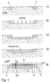
- the basic idea of the invention consists in a process step sequence, through which the gate areas are not next to each other, but are placed on top of each other, d. H. in the thickness direction of the Substrate SUB.
- an n-doped is first in the p-type substrate SUB Source region S and an n-doped drain region D are formed.
- the distance corresponds between the source region S and the drain region D of the Length dimension of the entire field effect transistor.
- 1B the range between S and D is up to etched to a depth that allows multiple gate areas to lay one on top of the other that this one source area S and have a drain region D in common.
- 1C is then followed a first gate area G1 in the area indicated by the etching Fig. 1B introduced etched area of the substrate. Subsequently is the first gate area G1 with a Silicon layer Si covered.
- Si is on this silicon layer 1E, a second gate region G2 is then formed such that he to lie between the source region S and the drain region D. comes, d. H. directly above the first gate area G1.
- the two superimposed gate areas G1 and G2 are then e.g. electrically connected to each other by a via DU.
- On the via can also be a Attach the input signal IN to the supply line.
- At the source area S can be an output line AUS and a drain line D can be a ground line GND can be contacted.
- a with the method shown in Fig. 1 and described above manufactured field effect transistor can, for. B. a MOS field effect transistor be, which, like previously used field effect transistors, has a rectangular shape.
- the electrical connection of the gate areas G1 and G2 Through contacting DU can also use other contacting methods one or both of the source area S and drain area D Connect exposed sides of the gate areas together.
Landscapes
- Metal-Oxide And Bipolar Metal-Oxide Semiconductor Integrated Circuits (AREA)
- Insulated Gate Type Field-Effect Transistor (AREA)
- Electrodes Of Semiconductors (AREA)
- Thin Film Transistor (AREA)
Abstract
Description
- Fig. 1A bis Fig. 1E
- schematisch Prozessschritte zur Herstellung eines erfindungsgemäßen Feldeffekttransistors in Form von Querschnitten durch einen Abschnitt einer integrierten Halbleiterschaltung;
- Fig. 2
- schematisch in ebener Draufsicht einen Substratbereich mit einem in integrierten Halbleiterschaltungen bislang üblichen Feldeffekttransistor, der zwei parallele streifenförmige Gatefinger aufweist; und
- Fig. 3
- schematisch den in Fig. 2 gezeigten herkömmlichen Feldeffekttransistor im Querschnitt.
Claims (2)
- Verfahren zur Herstellung von Feldeffekttransistoren, insbesondere MOS-Transistoren, in integrierten Halbleiterschaltungen mit folgenden Schritten:gekennzeichnet durch folgende Schritte:Schaffen von voneinander beabstandeten Source- und Drainbereichen (S, D) eines ersten Leitungstyps (n) in/auf einem Halbleitersubstrat (SUB) des entgegengesetzten Leitungstyps (p);Schaffen von mehreren Gatebereichen (G) jeweils zwischen einander zugeordneten benachbarten Source- und Drainbereichen (S, D), undelektrisches Verbinden der jeweiligen zu einem Feldeffekttransistor gehörigen Gatebereiche (G1, G2) untereinander, wobeidie mehreren jeweils zu einem Feldeffekttransistor gehörigen Gatebereiche (G1, G2) in Schichten übereinander in bzw. auf dem Halbleitersubstrat (SUB) in dessen Dickenrichtung gebildet werden, zwischen den übereinander angeordneten Gatebereichen (G1, G2) des Transistors eine Halbleiterschicht gebildet wird und jeweils ein Source- und Drainbereich allen übereinanderliegenden Gatebereichen gemeinsam ist,Ausätzen eines Substratabschnitts zwischen zwei einem Feldeffekttransistor zugeordneten Source- und Drainbereichen (S, D) von einer Hauptfläche des Substrats (SUB) aus;Bilden eines ersten Gatebereichs (Gl) in dem geätzten Substratabschnitt (SUB), so dass der erste Gatebereich (G1) zwischen dem Sourcebereich (S) und dem Drainbereich (D) liegt;Ausfüllen des geätzten Substratabschnitts oberhalb des ersten Gatebereichs (G1) mit Halbleitermaterial (Si);Schaffen wenigstens eines zweiten Gatebereichs (G2) oberhalb des ersten Gatebereichs (G1) unter Zwischenlage des eingefüllten Halbleitermaterials (Si) undVerbinden der Gatebereiche (G1, G2) an wenigstens einer Seite, die von dem Drain- und Sourcebereich (D, S) freiliegt, mit elektrisch gut leitendem Material.
- Verfahren nach Anspruch 1,
dadurch gekennzeichnet, dass ein den Feldeffekttransistor enthaltender Substratabschnitt ein p-dotierter Siliziumsubstratabschnitt ist, und dass die Drain- und Sourcebereiche n-Silizium und der Gatebereich SiO2 aufweisen.
Applications Claiming Priority (2)
| Application Number | Priority Date | Filing Date | Title |
|---|---|---|---|
| DE10045045A DE10045045C2 (de) | 2000-09-12 | 2000-09-12 | Herstellungsverfahren von Feldeffekttransistoren in integrierten Halbleiterschaltungen |
| DE10045045 | 2000-09-12 |
Publications (3)
| Publication Number | Publication Date |
|---|---|
| EP1187195A2 true EP1187195A2 (de) | 2002-03-13 |
| EP1187195A3 EP1187195A3 (de) | 2004-11-24 |
| EP1187195B1 EP1187195B1 (de) | 2006-12-13 |
Family
ID=7655908
Family Applications (1)
| Application Number | Title | Priority Date | Filing Date |
|---|---|---|---|
| EP01121016A Expired - Lifetime EP1187195B1 (de) | 2000-09-12 | 2001-08-31 | Verfahren zur Herstellung von Feldeffekttransistoren in integrierten Halbleiterschaltungen |
Country Status (6)
| Country | Link |
|---|---|
| US (1) | US6613616B2 (de) |
| EP (1) | EP1187195B1 (de) |
| JP (1) | JP3868778B2 (de) |
| KR (1) | KR100396636B1 (de) |
| DE (2) | DE10045045C2 (de) |
| TW (1) | TW518697B (de) |
Families Citing this family (1)
| Publication number | Priority date | Publication date | Assignee | Title |
|---|---|---|---|---|
| US8421810B2 (en) * | 2007-03-20 | 2013-04-16 | Thomson Licensing | Look-up table on film |
Family Cites Families (10)
| Publication number | Priority date | Publication date | Assignee | Title |
|---|---|---|---|---|
| JPS62224079A (ja) * | 1986-03-26 | 1987-10-02 | Sony Corp | 電界効果トランジスタ |
| JP2603886B2 (ja) * | 1991-05-09 | 1997-04-23 | 日本電信電話株式会社 | 薄層soi型絶縁ゲート型電界効果トランジスタの製造方法 |
| JP2572003B2 (ja) * | 1992-03-30 | 1997-01-16 | 三星電子株式会社 | 三次元マルチチャンネル構造を有する薄膜トランジスタの製造方法 |
| JP3460863B2 (ja) * | 1993-09-17 | 2003-10-27 | 三菱電機株式会社 | 半導体装置の製造方法 |
| US5604368A (en) * | 1994-07-15 | 1997-02-18 | International Business Machines Corporation | Self-aligned double-gate MOSFET by selective lateral epitaxy |
| US5705405A (en) * | 1994-09-30 | 1998-01-06 | Sgs-Thomson Microelectronics, Inc. | Method of making the film transistor with all-around gate electrode |
| JPH118390A (ja) * | 1997-06-18 | 1999-01-12 | Mitsubishi Electric Corp | 半導体装置及びその製造方法 |
| JP3086906B1 (ja) * | 1999-05-28 | 2000-09-11 | 工業技術院長 | 電界効果トランジスタ及びその製造方法 |
| DE19928564A1 (de) * | 1999-06-22 | 2001-01-04 | Infineon Technologies Ag | Mehrkanal-MOSFET und Verfahren zu seiner Herstellung |
| DE19938564A1 (de) * | 1999-08-19 | 2001-03-01 | Joh Georg Hartan Fa | Fahrgestell für einen Kinderwagen oder Puppenwagen |
-
2000
- 2000-09-12 DE DE10045045A patent/DE10045045C2/de not_active Expired - Fee Related
-
2001
- 2001-08-31 DE DE50111622T patent/DE50111622D1/de not_active Expired - Lifetime
- 2001-08-31 EP EP01121016A patent/EP1187195B1/de not_active Expired - Lifetime
- 2001-09-11 KR KR10-2001-0055728A patent/KR100396636B1/ko not_active Expired - Fee Related
- 2001-09-11 TW TW090122462A patent/TW518697B/zh not_active IP Right Cessation
- 2001-09-12 US US09/951,241 patent/US6613616B2/en not_active Expired - Lifetime
- 2001-09-12 JP JP2001277292A patent/JP3868778B2/ja not_active Expired - Fee Related
Also Published As
| Publication number | Publication date |
|---|---|
| US20020037639A1 (en) | 2002-03-28 |
| JP2002164443A (ja) | 2002-06-07 |
| JP3868778B2 (ja) | 2007-01-17 |
| EP1187195B1 (de) | 2006-12-13 |
| EP1187195A3 (de) | 2004-11-24 |
| DE10045045A1 (de) | 2002-04-04 |
| US6613616B2 (en) | 2003-09-02 |
| KR20020021028A (ko) | 2002-03-18 |
| DE50111622D1 (de) | 2007-01-25 |
| KR100396636B1 (ko) | 2003-09-02 |
| TW518697B (en) | 2003-01-21 |
| DE10045045C2 (de) | 2002-09-19 |
Similar Documents
| Publication | Publication Date | Title |
|---|---|---|
| DE69315239T2 (de) | VDMOS-Transistor mit verbesserter Durchbruchsspannungscharakteristik | |
| DE10250832B4 (de) | MOS-Transistor auf SOI-Substrat mit Source-Durchkontaktierung und Verfahren zur Herstellung eines solchen Transistors | |
| DE69122043T2 (de) | Vertikaler SOI-Feldeffekttransistor und dessen Herstellungsprozess | |
| DE2312413B2 (de) | Verfahren zur herstellung eines matrixschaltkreises | |
| DE2536270A1 (de) | Mii oeffnungen versehene halbleiterscheibe | |
| DE69505348T2 (de) | Hochspannungs-MOSFET mit Feldplatten-Elektrode und Verfahren zur Herstellung | |
| DE102014207415A1 (de) | Dicht gepackte Standardzellen für integrierte Schaltungsprodukte und Verfahren zu deren Herstellung | |
| DE102009025413A1 (de) | Vorrichtung, die eine Imidschicht mit Nichtkontaktöffnung umfasst, und Verfahren | |
| DE102014113519B4 (de) | Elektronisches Bauelement, Anordnung und Verfahren | |
| DE3913221A1 (de) | Halbleiteranordnung | |
| DE69226223T2 (de) | Kontaktausrichtung für Festwertspeicher | |
| DE69024234T2 (de) | Kondensator für eine integrierte Schaltung | |
| DE1616438C3 (de) | Integrierte Schaltung, Verwendung dieser Schaltung und Verfahren zu ihrer Herstellung | |
| DE10247431A1 (de) | Halbleitervorrichtung | |
| EP1187195B1 (de) | Verfahren zur Herstellung von Feldeffekttransistoren in integrierten Halbleiterschaltungen | |
| DE69422252T2 (de) | Halbleiteranordnung mit einem Halbleiterelement ausgestaltet in einer Mesastruktur | |
| DE102010055935B4 (de) | Verfahren zum Verbinden mehrerer ungehäuster Substrate | |
| DE4036958C2 (de) | Struktur zur Vermeidung von Feldkonzentrationen in einem Halbleiterbauelement und Verfahren zur Herstellung einer derartigen Struktur | |
| DE68923047T2 (de) | Verfahren zum Herstellen eines Kontaktes auf einer Halbleitereinrichtung und nach dem Verfahren hergestellte Halbleitereinrichtung. | |
| DE2737503A1 (de) | Feldeffekttransistor mit interdigitalstruktur und verfahren zu seiner herstellung | |
| DE3239204A1 (de) | Feldeffekt-transistorstruktur | |
| DE1918557A1 (de) | Integrierter Schaltkreis | |
| DE102023133256B3 (de) | Halbleiter-die und entsprechendes verfahren | |
| DE112019005134T5 (de) | Halbleitergerät und dieses verwendendes fahrzeugmontiertes elektronisches steuergerät | |
| DE102004023462B4 (de) | Verfahren zur Ausbildung von Leiterbahnstrukturen auf Halbleiterbauelementen |
Legal Events
| Date | Code | Title | Description |
|---|---|---|---|
| PUAI | Public reference made under article 153(3) epc to a published international application that has entered the european phase |
Free format text: ORIGINAL CODE: 0009012 |
|
| AK | Designated contracting states |
Kind code of ref document: A2 Designated state(s): AT BE CH CY DE DK ES FI FR GB GR IE IT LI LU MC NL PT SE TR |
|
| AX | Request for extension of the european patent |
Free format text: AL;LT;LV;MK;RO;SI |
|
| PUAL | Search report despatched |
Free format text: ORIGINAL CODE: 0009013 |
|
| AK | Designated contracting states |
Kind code of ref document: A3 Designated state(s): AT BE CH CY DE DK ES FI FR GB GR IE IT LI LU MC NL PT SE TR |
|
| AX | Request for extension of the european patent |
Extension state: AL LT LV MK RO SI |
|
| RIC1 | Information provided on ipc code assigned before grant |
Ipc: 7H 01L 21/8234 A Ipc: 7H 01L 27/088 B Ipc: 7H 01L 29/78 B |
|
| 17P | Request for examination filed |
Effective date: 20050520 |
|
| AKX | Designation fees paid |
Designated state(s): DE FR GB IE IT |
|
| GRAP | Despatch of communication of intention to grant a patent |
Free format text: ORIGINAL CODE: EPIDOSNIGR1 |
|
| RTI1 | Title (correction) |
Free format text: METHOD OF MANUFACTURING FIELD EFFECT TRANSISTORS IN INTEGRATED SEMICONDUCTOR CIRCUITS |
|
| RAP1 | Party data changed (applicant data changed or rights of an application transferred) |
Owner name: QIMONDA AG |
|
| GRAS | Grant fee paid |
Free format text: ORIGINAL CODE: EPIDOSNIGR3 |
|
| GRAA | (expected) grant |
Free format text: ORIGINAL CODE: 0009210 |
|
| AK | Designated contracting states |
Kind code of ref document: B1 Designated state(s): DE FR GB IE IT |
|
| PG25 | Lapsed in a contracting state [announced via postgrant information from national office to epo] |
Ref country code: IT Free format text: LAPSE BECAUSE OF FAILURE TO SUBMIT A TRANSLATION OF THE DESCRIPTION OR TO PAY THE FEE WITHIN THE PRESCRIBED TIME-LIMIT;WARNING: LAPSES OF ITALIAN PATENTS WITH EFFECTIVE DATE BEFORE 2007 MAY HAVE OCCURRED AT ANY TIME BEFORE 2007. THE CORRECT EFFECTIVE DATE MAY BE DIFFERENT FROM THE ONE RECORDED. Effective date: 20061213 Ref country code: IE Free format text: LAPSE BECAUSE OF FAILURE TO SUBMIT A TRANSLATION OF THE DESCRIPTION OR TO PAY THE FEE WITHIN THE PRESCRIBED TIME-LIMIT Effective date: 20061213 |
|
| REG | Reference to a national code |
Ref country code: GB Ref legal event code: FG4D Free format text: NOT ENGLISH |
|
| REG | Reference to a national code |
Ref country code: IE Ref legal event code: FG4D Free format text: LANGUAGE OF EP DOCUMENT: GERMAN |
|
| REF | Corresponds to: |
Ref document number: 50111622 Country of ref document: DE Date of ref document: 20070125 Kind code of ref document: P |
|
| GBV | Gb: ep patent (uk) treated as always having been void in accordance with gb section 77(7)/1977 [no translation filed] |
Effective date: 20061213 |
|
| EN | Fr: translation not filed | ||
| PLBE | No opposition filed within time limit |
Free format text: ORIGINAL CODE: 0009261 |
|
| STAA | Information on the status of an ep patent application or granted ep patent |
Free format text: STATUS: NO OPPOSITION FILED WITHIN TIME LIMIT |
|
| 26N | No opposition filed |
Effective date: 20070914 |
|
| PG25 | Lapsed in a contracting state [announced via postgrant information from national office to epo] |
Ref country code: GB Free format text: LAPSE BECAUSE OF FAILURE TO SUBMIT A TRANSLATION OF THE DESCRIPTION OR TO PAY THE FEE WITHIN THE PRESCRIBED TIME-LIMIT Effective date: 20061213 |
|
| PG25 | Lapsed in a contracting state [announced via postgrant information from national office to epo] |
Ref country code: FR Free format text: LAPSE BECAUSE OF FAILURE TO SUBMIT A TRANSLATION OF THE DESCRIPTION OR TO PAY THE FEE WITHIN THE PRESCRIBED TIME-LIMIT Effective date: 20070803 |
|
| PG25 | Lapsed in a contracting state [announced via postgrant information from national office to epo] |
Ref country code: FR Free format text: LAPSE BECAUSE OF FAILURE TO SUBMIT A TRANSLATION OF THE DESCRIPTION OR TO PAY THE FEE WITHIN THE PRESCRIBED TIME-LIMIT Effective date: 20061213 |
|
| REG | Reference to a national code |
Ref country code: DE Ref legal event code: R081 Ref document number: 50111622 Country of ref document: DE Owner name: INFINEON TECHNOLOGIES AG, DE Free format text: FORMER OWNER: QIMONDA AG, 81739 MUENCHEN, DE Ref country code: DE Ref legal event code: R081 Ref document number: 50111622 Country of ref document: DE Owner name: POLARIS INNOVATIONS LTD., IE Free format text: FORMER OWNER: QIMONDA AG, 81739 MUENCHEN, DE |
|
| REG | Reference to a national code |
Ref country code: DE Ref legal event code: R081 Ref document number: 50111622 Country of ref document: DE Owner name: POLARIS INNOVATIONS LTD., IE Free format text: FORMER OWNER: INFINEON TECHNOLOGIES AG, 85579 NEUBIBERG, DE |
|
| PGFP | Annual fee paid to national office [announced via postgrant information from national office to epo] |
Ref country code: DE Payment date: 20150929 Year of fee payment: 15 |
|
| REG | Reference to a national code |
Ref country code: DE Ref legal event code: R119 Ref document number: 50111622 Country of ref document: DE |
|
| PG25 | Lapsed in a contracting state [announced via postgrant information from national office to epo] |
Ref country code: DE Free format text: LAPSE BECAUSE OF NON-PAYMENT OF DUE FEES Effective date: 20170301 |