EP1139384B1 - Elektronenoptische Anordnung, Verfahren zur Herstellung derselben, Ladungsträgerteilchenstrahl-Belichtungsgerät und Verfahren zur Herstellung der zugehörigen Vorrichtung - Google Patents
Elektronenoptische Anordnung, Verfahren zur Herstellung derselben, Ladungsträgerteilchenstrahl-Belichtungsgerät und Verfahren zur Herstellung der zugehörigen Vorrichtung Download PDFInfo
- Publication number
- EP1139384B1 EP1139384B1 EP01303029A EP01303029A EP1139384B1 EP 1139384 B1 EP1139384 B1 EP 1139384B1 EP 01303029 A EP01303029 A EP 01303029A EP 01303029 A EP01303029 A EP 01303029A EP 1139384 B1 EP1139384 B1 EP 1139384B1
- Authority
- EP
- European Patent Office
- Prior art keywords
- electrodes
- charged
- optical system
- array according
- electrode
- Prior art date
- Legal status (The legal status is an assumption and is not a legal conclusion. Google has not performed a legal analysis and makes no representation as to the accuracy of the status listed.)
- Expired - Lifetime
Links
Images


Classifications
-
- H—ELECTRICITY
- H01—ELECTRIC ELEMENTS
- H01J—ELECTRIC DISCHARGE TUBES OR DISCHARGE LAMPS
- H01J37/00—Discharge tubes with provision for introducing objects or material to be exposed to the discharge, e.g. for the purpose of examination or processing thereof
- H01J37/30—Electron-beam or ion-beam tubes for localised treatment of objects
- H01J37/317—Electron-beam or ion-beam tubes for localised treatment of objects for changing properties of the objects or for applying thin layers thereon, e.g. for ion implantation
- H01J37/3174—Particle-beam lithography, e.g. electron beam lithography
-
- B—PERFORMING OPERATIONS; TRANSPORTING
- B82—NANOTECHNOLOGY
- B82Y—SPECIFIC USES OR APPLICATIONS OF NANOSTRUCTURES; MEASUREMENT OR ANALYSIS OF NANOSTRUCTURES; MANUFACTURE OR TREATMENT OF NANOSTRUCTURES
- B82Y10/00—Nanotechnology for information processing, storage or transmission, e.g. quantum computing or single electron logic
-
- B—PERFORMING OPERATIONS; TRANSPORTING
- B82—NANOTECHNOLOGY
- B82Y—SPECIFIC USES OR APPLICATIONS OF NANOSTRUCTURES; MEASUREMENT OR ANALYSIS OF NANOSTRUCTURES; MANUFACTURE OR TREATMENT OF NANOSTRUCTURES
- B82Y40/00—Manufacture or treatment of nanostructures
-
- H—ELECTRICITY
- H01—ELECTRIC ELEMENTS
- H01J—ELECTRIC DISCHARGE TUBES OR DISCHARGE LAMPS
- H01J37/00—Discharge tubes with provision for introducing objects or material to be exposed to the discharge, e.g. for the purpose of examination or processing thereof
- H01J37/02—Details
- H01J37/04—Arrangements of electrodes and associated parts for generating or controlling the discharge, e.g. electron-optical arrangement, ion-optical arrangement
- H01J37/10—Lenses
- H01J37/12—Lenses electrostatic
-
- H—ELECTRICITY
- H01—ELECTRIC ELEMENTS
- H01J—ELECTRIC DISCHARGE TUBES OR DISCHARGE LAMPS
- H01J2237/00—Discharge tubes exposing object to beam, e.g. for analysis treatment, etching, imaging
- H01J2237/10—Lenses
- H01J2237/12—Lenses electrostatic
- H01J2237/1205—Microlenses
Definitions
- the present invention relates to an charged-particle optical system array suitable for an exposure apparatus using charged-particle beams such as electron beams and, more particularly, to an charged particle optical system array having a plurality of charged-particle lenses.
- an electron beam exposure technique receives a great deal of attention as a promising candidate of lithography capable of micro-pattern exposure at a line width of 0.1 mu m or less.
- An example is a variable rectangular beam method of drawing a pattern with one stroke. This method suffers many problems as a mass-production exposure apparatus because of a low throughput.
- a pattern projection method of reducing and transferring a pattern formed on a stencil mask This method is advantageous to a simple repetitive pattern but disadvantageous to a random pattern such as a logic interconnection pattern in terms of the throughput, and a low productivity disables practical application.
- a multi-beam system for drawing a pattern simultaneously with a plurality of electron beams without fusing any mask has been proposed and is very advantageous to practical use because of the absence of physical mask formation and exchange.
- What is important in using multi-electron beams is the number of electron lenses formed in an array used in an electron optical system. The number of electron lenses determines the number of electron beams, and is a main factor which determines the throughput.
- Downsizing while improving the performance of the electron optical system array is one of keys to improve the performance of the multi-beam exposure apparatus.
- Electron lenses are classified into electromagnetic and electrostatic types.
- the electrostatic electron lens does not require any coil core or the like, is simpler in structure than the electromagnetic electron lens, and is more advantageous to downsizing. Principal prior arts concerning downsizing of the electrostatic electron lens (electrostatic lens) will be described.
- United States Patent (USP) No. 4,419,580 proposes an electron optical system array in which electron lenses are two-dimensionally arrayed on an Si substrate and electrodes are aligned by V-grooves and cylindrical spacers.
- K.Y. Lee et al. J. Vac. Sci. Technol. B12(6), Nov/Dec 1994, pp. 3,425 - 3,430 ) disclose a multilayered structure of Si and Pyrex glass fabricated by using anodic bonding, and provides microcolumn electron lenses aligned at a high precision.
- the electron optical system array disclosed by K.Y. Lee et al. suffers various problems which should be solved, such that 1) glass may not be sandwiched at a small electrode interval, and 2) anodic bonding must be repeated many times and the process is complicated (bonding must be repeated 2 (n-1) times).
- Document GB-A-1 211 616 discloses a charged-particle beam fabrication of microelectronic circuit patterns where a charged-particle optical system according to the preamble of claim 1 is described.
- Document US-A-5 981 954 discloses an electron beam exposure apparatus, which has an electron source for emitting an electron beam, and an irradiation electron, optical system which is arranged between the electron source and a first object, including a portion for transmitting an electron beam, and includes a plurality of electron lenses, and projects the electron beam transmitted through the first object onto a second object to expose it via a reduction electron optical system, acquires information associated with the intensity distribution of the electron beams to be irradiated onto the first object, and adjusts the electron optical characteristics of the irradiation electron optical system on the basis of the acquired information associated with the intensity distribution.
- the present invention has been made to overcome the conventional drawbacks, and has as its principal object to provide an improvement of the prior arts. It is an object of the present invention to provide an improved charged-particle system array which realizes various conditions such as downsizing, high precision, and high reliability at high level. It is another object of the present invention to provide a method of manufacturing such a charged-particle optical system array, a high-precision exposure apparatus using the charged-particle optical system array, and a high-productivity device manufacturing method.
- the number of electrodes which form the nested structure is typically two or three, but may be four or more.
- the electron optical system array comprises the first, second, and third electrodes 1, 2, and 3 respectively having membranes 1A, 2A, and 3A in which a plurality of apertures are formed on the paths of a plurality of electron beams (charged-particle beams), and support substrates 1B, 2B, and 3B which support corresponding membranes. These membranes are spatially insulated.
- the support substrates of the first to third electrodes are held by the single base substrate 4.
- the three electrodes form a nested structure such that the support substrate 2B of the second electrode 2 is located-inside the support substrate 1B of the first electrode 1 and the support substrate 3B of the third electrode 3 is located inside the support substrate 2B of the second electrode 2.
- the first embodiment exemplifies only 3 x 3 apertures for each electrode, but in practice the electrode can have a larger number of apertures (e.g., 8 x 8 apertures).
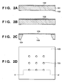
- FIGs. 2A to 2D show a method of forming the upper and lower electrodes 1 and 3.
- the method of forming the upper and lower electrodes 1 and 3 will be described with reference to Figs. 2A to 2D .
- These electrodes have different shapes and sizes, as shown in Fig. 1 .
- a silicon wafer of the ⁇ 100> direction is prepared as a substrate 101, and 300-nm thick SiO 2 films are formed as mask layers 102 on the two surfaces of the substrate 101 by thermal oxidation. Portions of one mask layer 102 that serve as a prospective hollow portion and alignment grooves are removed by patterning the mask layer 102 by resist and etching processes ( Fig. 2A ).
- the size and thickness of the substrate 101 can be appropriately selected in accordance with the sizes of the first and third electrodes 1 and 3.
- Titanium and copper are successively deposited to film thicknesses of 5 nm and 5 ⁇ m on the upper surface of the substrate, and patterned by resist and etching processes to form an electrode layer 103 having a plurality of apertures 105 at prospective paths of electron beams (charged-particle beams).
- the deposition method is, e.g., deposition using resistance heating or an electron beam, or sputtering.
- titanium/gold or titanium/platinum may be used ( Fig. 2B ).
- the electrode layer 103 is protected with polyimide.
- the silicon substrate 101 is etched back from the other surface at 90°C by using a 22% aqueous tetramethylammonium hydroxide solution. Etching is continued until silicon is etched away and the other mask layer 102 is exposed, thereby forming a hollow portion 106 and alignment grooves 104.
- the substrate is cleaned with water and dried.
- the mask layer 102 exposed after dry etching of silicon is etched away by using tetrafluoromethane in a dry etching apparatus.
- the polyimide film used to protect the other surface is removed by ashing.
- the upper and lower electrodes 1 and 3 each having a plurality of apertures 105 on prospective electron beam paths are obtained ( Fig. 2C).
- Fig. 2D is a plan view of the completed electrode shown in Fig. 2C .
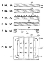
- a method of forming the middle electrode 2 will be described with reference to Figs. 3A to 3F .
- a silicon wafer of the ⁇ 100> direction is prepared as a substrate 201, and 300-nm thick SiO 2 films are formed as mask layers 202 on the two surfaces of the substrate 201 by thermal oxidation. Portions.of one mask layer 202 that serve as a prospective hollow portion and alignment grooves are removed by patterning the mask layer 202 by resist and etching processes ( Fig. 3A ).
- Chromium and gold are deposited as a plating electrode 203 to film thicknesses of 5 nm and 100 nm ( Fig. 3B ).
- a resist pattern 204 serving as a plating mold is formed on the plating electrode 203.
- the resist is formed to a film thickness of 60 ⁇ m by using SU-8 (Micro Chem. Co) mainly consisting of an epoxidized bisphenol A oligomer.
- Exposure is performed for, e.g., 60 sec by a contact type exposure apparatus using a high-pressure mercury lamp. After exposure, post-exposure bake (PEB) is done on a hot plate at 85°C for 30 min.
- PEB post-exposure bake
- the resist is developed with propylene glycol monomethyl ether acetate for 5 min to complete the plating mold pattern 204.
- a polyvinylphenol-based or cyclized rubber-based negative resist or a novolac-based positive resist can be used.
- the resist may be applied a plurality of number of times ( Fig. 3C ).
- the gaps of the resist 204 are filled with an electrode layer by electroplating, thus forming an electrode layer 205 having alignment grooves 208 in addition to a plurality of apertures at prospective electron beam paths. More specifically, the gaps of the resist pattern 204 can be filled with a 50- ⁇ m thick copper pattern by electroplating using, e.g., an acid copper plating solution at a plating solution flow rate of 5 L/min, a current density of 7.5 mA/cm 2 , and a solution temperature of 28°C for 6 h and 40 min.
- the SU-8 resist 204 is removed in N-methylpyrrolidone (NMP) at 80°C, and the substrate is cleaned and dried by IPA to obtain a copper pattern as the electrode layer 205.
- the metal which forms the electrode layer can be a nonmagnetic material such as gold or platinum, other than copper ( Fig. 3D ).
- the plating surface is protected with polyimide (not shown).
- the silicon substrate 201 is etched back from the other surface at 90°C by using a 22% aqueous tetramethylammonium hydroxide solution until the other mask layer 202 is exposed. Etching is continued until silicon is etched away and the mask layer 202 is exposed, thereby forming a hollow portion 206 and alignment grooves 209.
- the substrate is cleaned with water and dried.
- the mask layer 202 and plating electrode 203 exposed after dry etching of silicon are etched away by using tetrafluoromethane in a dry etching apparatus.
- the polyimide film which protects the other surface is removed by ashing to complete the middle electrode, 2 ( Fig. 3E). Fig.
- FIG. 3F is a plan view of the competed middle electrode 2 shown in Fig. 3E .
- the first embodiment forms the divided electrodes 205 for grouping arrayed apertures in units of columns.
- the electrode fabricated by plating is higher in conductivity and higher in electrode performance than a doped-silicon electrode.
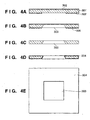
- a method of forming the base substrate 4 is shown in Figs. 4A to 4E .
- a silicon wafer of the ⁇ 100> direction is prepared as a substrate 301, and 300-nm thick SiO 2 films are formed as mask layers 302 on the two surfaces of the substrate by thermal oxidation. Portions of one mask layer 302 that serve as a prospective through hole and alignment grooves are removed by patterning the mask layer 302 by resist and etching processes ( Fig. 4A ).
- the silicon substrate 301 is etched back at 90°C by using a 22% aqueous tetramethylammonium hydroxide solution until the other mask layer 302 is exposed. At this time, alignment grooves 305 are formed ( Fig. 4B ).
- the remaining mask layer 302 is removed by using an aqueous solution mixture of hydrogen fluoride and ammonium fluoride, thereby forming a through hole 303 ( Fig. 4C ).
- a 300-nm thick SiO 2 layer 304 is formed as an insulating layer on the entire surface of the substrate by thermal oxidation ( Fig. 4D).
- Fig. 4E is a plan view of the completed base substrate 4 shown in Fig. 4D .
- the electrodes 1, 2, and 3 fabricated in this manner are aligned and joined to the base substrate 4 in the following procedures.
- the lower electrode 3 is first joined and fixed to the upper surface of the base substrate 4.
- the middle electrode 2 is joined and fixed to the upper surface of the base substrate 4.
- the upper electrode 1 is joined and fixed to the upper surface of the base substrate 4.
- an aqueous hydrofluoric acid solution is applied to a joining portion, alignment grooves are observed with an infrared camera, and substrates are aligned such that all the alignment grooves overlap each other. After that, the two substrates are joined.
- substrates may be joined with an adhesive. In this case, an adhesive almost free from degassing in vacuum is selected.
- the electron optical system array having this structure exhibits the following excellent effects because of the nested structure of electrodes, and can realize various conditions such as downsizing, high precision, and high reliability at high level.
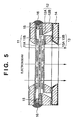
- Fig. 5 is a sectional view showing an electron optical system array according to the second embodiment of the present invention.
- middle and lower electrodes 12 and 13 are fixed to a base substrate 14 to form a nested structure, whereas an upper electrode 11 is fixed to the middle electrode 12 without nesting.
- the upper and middle electrodes 11 and 12 are fixed with an adhesive 16 via spacers 15 such as fibers, and the outer size of the spacer 15 determines the substrate interval.
- reference numerals 11A, 12A, and 13A denote membranes of the upper, middle, and lower electrodes 11, 12, and 13, respectively; and 11B, 12B, and 13B, membrane support substrates of the upper, middle, and lower electrodes 11, 12, and 13.
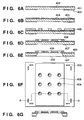
- Figs. 6A to 6F show a method of forming the upper and lower electrodes 11 and 13.
- the method of forming the upper and lower electrodes 11 and 13 will be explained with reference to Figs. 6A to 6F .
- These electrodes have different shapes and sizes, as shown in Fig. 5 .
- a silicon wafer of the ⁇ 100> direction is prepared as a substrate 401, and 300-nm thick SiO 2 layers are formed as mask layers 402 on the two surfaces of the substrate 401 by thermal oxidation. Portions of one mask layer that serve as a prospective hollow portion and alignment grooves are removed by patterning the mask layer by resist and etching processes ( Fig. 6A ).
- Titanium and copper are successively deposited to film thicknesses of 5 nm and 5 ⁇ m, and patterned by resist and etching processes to form an electrode layer 404 having alignment grooves 403.
- the deposition method is, e.g., deposition using resistance heating or an electron beam, or sputtering.
- titanium/gold or titanium/platinum may be used ( Fig. 6B ).
- a resist pattern 405 serving as a plating mold is formed on the electrode layer 404.
- the resist adopts SU-8, and its film thickness is 110 ⁇ m ( Fig. 6C ).
- shield electrodes 406 are formed in the openings of the resist 405 by electroplating copper.
- the SU-8 resist 405 is removed in N-methylpyrrolidone (NMP) at 80°C, and the substrate is cleaned and dried by IPA to obtain a copper pattern as the shield electrodes 406 ( Fig. 6D ).
- NMP N-methylpyrrolidone
- the plating surface is protected with polyimide (not shown).
- the silicon substrate 401 is etched back from the other surface at 90°C by using a 22% aqueous tetramethylammonium hydroxide solution. Etching is continued until silicon is etched away and the other mask layer 402 is exposed, thereby forming a hollow portion 409 and alignment grooves 407.
- the substrate is cleaned with water and dried.
- the mask layer exposed after dry etching of silicon is etched away by using tetrafluoromethane in a dry etching apparatus.
- the polyimide film which protects the other surface is removed by ashing to complete the upper and lower electrodes 11 and 13 each having a plurality of apertures at prospective electron beam paths ( Fig. 6E).
- Fig. 6F is a plan view of the completed electrode shown in Fig. 6F .
- the two ends of the substrate are finally cut, as shown in Fig. 6G .
- Cutting can be done with a device such as a dicing saw or laser cutter used in a semiconductor manufacturing process.
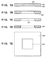
- Figs. 7A to 7E are views showing a method of forming the base substrate 14.
- a silicon wafer of the ⁇ 100> direction is prepared as a substrate 501, and 300-nm thick SiO 2 layers are formed as mask layers 502 on the two surfaces of the substrate by thermal oxidation. Portions of one mask layer 502 that serve as a prospective through hole and alignment grooves are removed by patterning the mask layer 502 by resist and etching processes ( Fig. 7A ).
- the silicon substrate is etched back at 90°C by using a 22% aqueous tetramethylammonium hydroxide solution until the other mask layer 502 is exposed. At this time, alignment grooves 503 are formed ( Fig. 7B ).
- the remaining mask layer 502 is removed by using an aqueous solution mixture of hydrogen fluoride and ammonium fluoride, thereby forming a through hole 504 ( Fig. 7C ).
- a 300-nm thick SiO 2 film is formed as an insulating layer 505 on the entire surface of the substrate by thermal oxidation ( Fig. 7D).
- Fig. 7E is a plan view of the electrode shown in Fig. 7D .
- the electrodes 11, 12, and 13 fabricated in this way are aligned and joined to the base substrate 14 in the following procedures.
- the lower electrode 13 is first joined and fixed to the upper surface of the base substrate 14.
- the middle electrodes 12 is joined and fixed to the upper surface of the base substrate 14.
- an aqueous hydrofluoric acid solution is applied to a joining portion, and the electrode is aligned and joined while observed with an infrared camera.
- the upper electrode 11 is joined and fixed to the upper surface of the middle electrode 12.
- the upper and middle electrodes 11 and 12 are joined with the adhesive 16 after they are aligned to locate the spacers 15 in the alignment grooves of the two substrates. As the adhesive, one almost free from degassing in vacuum is selected.
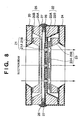
- Fig. 8 is a sectional view showing an electron optical system array according to the third embodiment of the present invention.
- This electron optical system array employs a shield electrode 25 between upper and middle electrodes 21 and 22. More specifically, the electron optical system array has two units respectively made up of the upper electrode 21 and shield electrode 25 of a nested structure that are fixed to a base substrate 20, and a lower electrode 23 and the middle electrode 22 that are fixed to a base substrate 24. These units are fixed with an adhesive 27 via spacers 26.
- reference numerals 21A, 22A, 23A, and 25A denote membranes of the upper, middle, lower, and shield electrodes 21, 22, 23, and 25, respectively; and 21B, 22B, 23B, and 25B, membrane support substrates of the upper, middle, lower, and shield electrodes 21, 22, 23, and 25.
- Figs. 9A to 9F are views for explaining a method of forming the middle electrode 22.
- a silicon wafer 601 of the ⁇ 100> direction is prepared, and 300-nm thick SiO 2 layers are formed as mask layers 602 on the two surfaces of the substrate 601 by thermal oxidation. Portions of one mask layer 602 that serve as a prospective hollow portion and alignment grooves are removed by patterning the mask slayer 602 by resist and etching processes ( Fig. 9A ).
- the silicon substrate is anisotropically etched by using an aqueous potassium hydroxide solution to form a 50- ⁇ m thick membrane portion 604, a hollow portion 606, and alignment grooves 605 and 607 ( Fig. 9B ).
- a resist is applied and patterned by photolithography.
- the mask layer 602 and silicon substrate 601 are etched by reactive ion etching using the patterned resist as a mask, thus forming a plurality of apertures 608 at prospective electron beam paths ( Fig. 9C ).
- the mask layers 602 on the two surfaces are removed by using an aqueous solution mixture of hydrofluoric acid and ammonium fluoride ( Fig. 9D ).
- a 300-nm thick SiO 2 film is formed as an insulating layer 609 by thermal oxidation so as to cover the substrate ( Fig. 9E ).
- a 50-nm thick Ti film and 100-nm thick Au film are formed by vacuum evaporation, and patterned by photolithography to form divided wiring lines 610 ( Fig. 9F ).
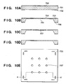
- Figs. 10A to 10E are views for explaining a method of forming the shield electrode 25.
- a silicon wafer 701 of the ⁇ 100> direction which is made conductive by doping an impurity is prepared, and 300-nm thick SiO 2 layers are formed as mask layers 702 on the two surfaces of the substrate 701 by thermal oxidation. Portions of one mask layer 702 that serve as a prospective hollow portion and alignment grooves are removed by patterning the mask layer 702 by photolithography and etching processes ( Fig. 10A ).
- the silicon wafer is etched from the lower surface at 90°C by using a 22% aqueous tetramethylammonium hydroxide solution, thus forming a 20- ⁇ m thick membrane portion 704, a hollow portion 705, and alignment grooves 703 and 706 ( Fig. 10B ).
- the mask layer 702 on the upper surface and the silicon substrate are etched by photolithography and dry etching processes to form a plurality of apertures 707 ( Fig. 10C ).
- Fig. 10D The mask layer 702 on the upper surface is removed by reactive ion etching using CF 4 gas ( Fig. 10D).
- Fig. 10E is a plan view of the shield electrode shown in Fig. 10D .
- the upper and lower electrodes 21 and 23 can be formed following the same procedures as in the second embodiment.
- the electrodes 21, 22, 23 and shield electrode 25 formed in this fashion are aligned and joined to the base substrates 20 and 24 in the following procedures.
- the lower electrode 23 is first joined and fixed to the upper surface of the base substrate 24.
- the middle electrode 22 is joined and fixed to the upper surface of the base substrate 24.
- an aqueous hydrofluoric acid solution is applied to a joining portion, and the electrode is aligned and joined while observed with an infrared camera.
- the upper electrode 21 is joined and fixed to the base substrate 20, and the shield electrode 25 is joined and fixed to the same surface of the base substrate 20.
- the two units are aligned via the spacers 26 and fixed with the adhesive 27.
- Fig. 11 is a sectional view showing an electron optical system array according to the fourth embodiment of the present invention.
- the fourth embodiment adopts two sets of the electrodes 1, 2, and 3 in the first embodiment. More specifically, in this electron optical system array, first, second, and third electrodes 1a, 2a, and 3a corresponding to the electrodes 1, 2, and 3 of the first embodiment are supported by one surface of a base substrate 4, whereas fourth, fifth, and sixth electrodes 3b, 2b, and 1b corresponding to the electrodes 3, 2, and 1 of the first embodiment are supported by the other surface of the base substrate 4.
- This arrangement uses one base substrate as a position reference, so that an electron optical system array having a high alignment accuracy between electrodes can be attained.
- This multi-stage electron optical system array is suitable when only a one-stage electron lens cannot provide a sufficient lens power.
- one electron optical system array is comprised of two sets of the electrodes 1, 2, and 3 of the first embodiment.
- one electron optical system array may be constituted by three or more sets of electrodes.
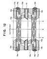
- Fig. 12 is a sectional view showing an electron optical system array according to the fifth embodiment of the present invention.
- the fifth embodiment adopts two sets of the electrodes 11, 12, and 13 in the second embodiment. More specifically, in this electron optical system array, first, second, and third electrodes 11a, 12a, and 13a corresponding to the electrodes 11, 12, and 13 of the second-embodiment are supported by one surface of a base substrate 12, whereas fourth, fifth, and sixth electrodes 13b, 12b, and 11b corresponding to the electrodes 13, 12, and 11 of the second embodiment are supported by the other surface of the base substrate 12. Since this arrangement uses one base substrate as a position reference, an electron optical system array having a high alignment accuracy between two electron optical system arrays can be obtained. This multi-stage electron optical system array is suitable when only a one-stage electron lens cannot provide a sufficient lens power.
- one electron optical system array is comprised of two sets of the electrodes 11, 12, and 13 of the second embodiment.
- one electron optical system array may be constituted by three or more sets of electrodes.
- Fig. 13 is a sectional view showing an electron optical system array according to the sixth embodiment of the present invention.
- the sixth embodiment employs two sets of the electrodes 21, 22, and 23 in the third embodiment. More specifically, this electron optical system array comprises a set of first, second, and third electrodes 21a, 22a, and 23a corresponding to the electrodes 21, 22, and 23 of the third embodiment, and a set of fourth, fifth, and sixth electrodes 23b, 22b, and 21b corresponding to the electrodes 23, 22, and 21 of the third embodiment.
- This arrangement uses one base substrate as a position reference, and thus an electron optical system array having a high alignment accuracy between two electron optical system arrays can be obtained.
- This multi-stage electron optical system array is suitable when only a one-stage electron lens cannot provide a sufficient lens power.
- one electron optical system array is comprised of two sets of the electrodes 21, 22, and 23 of the third embodiment.
- one electron optical system array may be constituted by three or more sets of electrodes.
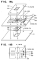
- FIG. 14A is a perspective view of an assembly
- Fig. 14B is a plan view.
- the support substrate 11B of the upper electrode 11 (11a, 11b) is smaller in size than the support substrate 12B of the middle electrode 12 (12a, 12b).
- the middle electrode 12 (12a, 12b) and lower electrode 13 (13a, 13b) are fixed to the base substrate 14 so as to form a nested structure, and the upper electrode 11 (11a, 11b) faces the middle electrode 12 (12a, 12b).
- parts 921, 922 and 923 of the membrane 12A of the middle electrode 12 (12a, 12b) are exposed, which facilitates wiring to the middle electrode 12 (12a, 12b) by wire bonding or the like.
- a plurality of arrayed apertures of the middle electrode are grouped in units of columns, and each of the grouped columns receives the same potential.
- the first column receives a potential via a wiring line 901
- the second column receives a potential via a wiring line 902
- the third column receives a potential via a wiring line 903.
- FIG. 15 is a schematic view showing the overall system.
- an electron gun 501 as a charged-particle source is constituted by a cathode 501a, grid 501b, and anode 501c. Electrons emitted by the cathode 501a form a crossover image (to be referred to as an electron source ES hereinafter) between the grid 501b and the anode 501c.
- An electron beam emitted by the electron source ES irradiates a correction electron optical system 503 via an irradiation electron optical system 502 serving as a condenser lens.
- the irradiation electron optical system 502 is comprised of electron lenses (Einzel lenses) 521 and 522 each having three aperture electrodes.
- the correction electron optical system 503 includes an electron optical system array to which the electron optical system array is applied, and forms a plurality of intermediate images of the electron source ES (details of the structure will be described later).
- the correction electron optical system 503 adjusts the formation positions of intermediate images so as to correct the influence of aberration of a protection electron optical system 504.
- Each intermediate image formed by the correction electron optical system 503 is reduced and projected by the projection electron optical system 504, and forms an image of the electron source ES on a wafer 505 as a surface to be exposed.
- the projection electron optical system 504 is constituted by a symmetrical magnetic doublet made up of a first projection lens 541 (543) and second projection lens 542 (544).
- Reference numeral 506 denotes a deflector for deflecting a plurality of electron beams from the correction electron optical system 503 and simultaneously displacing a plurality of electron source images on the wafer 505 in the X and Y directions; 507, a dynamic focus coil for correcting a shift in the focal position of an electron source image caused by deflection aberration generated when the deflector 506 operates; 508, a dynamic stigmatic coil for correcting astigmatism among deflection aberrations generated by deflection; 509, a ⁇ -Z stage which supports the wafer 505, is movable in the optical axis AX (Z-axis) direction and the rotational direction around the Z-axis, and has a stage reference plate 510 fixed thereto; 511, an X-Y stage which supports the ⁇ -Z stage and is movable in the X and Y directions perpendicular to the optical axis AX (Z-axis); and 512, a reflected-electron detector for
- Figs. 16A and 16B are views for explaining details of the correction electron optical system 503.
- the correction electron optical system 503 comprises an aperture array AA, blanker array BA, element electron optical system array unit LAU, and stopper array SA along the optical axis.
- Fig. 16A is a view of the correction electron optical system 503 when viewed from the electron gun 501
- Fig. 16B is a sectional view taken along the line A - A' in Fig. 16A .
- the aperture array AA has an array (8 x 8) of apertures regularly formed in a substrate, and splits an incident electron beam into a plurality of (64) electron beams.
- the blanker array BA is constituted by forming on one substrate a plurality of deflectors for individually deflecting a plurality of electron beams split by the aperture array AA.
- the element electron optical system array unit LAU is formed from first and second electron optical system arrays LA1 and LA2 as electron lens arrays each prepared by two-dimensionally arraying a plurality of electron lenses on the same surface.
- the electron optical system arrays LA1 and LA2 have a structure as an application of the electron optical system array described in the above embodiments to an 8 x 8 array.
- the first and second electron optical system arrays LA1 and LA2 are fabricated by the above-mentioned method.
- the element electron optical system array unit LAU constitutes one element electron optical system EL by the electron lenses of the first and second electron optical system arrays LA1 and LA2 that use the common X-Y coordinate system.
- the stopper array SA has a plurality of apertures formed in a substrate, similar to the aperture array AA. Only a beam deflected by the blanker array BA is shielded by the stopper array SA, and ON/OFF operation of an incident beam to the wafer 505 is switched for each beam under the control of the blanker array.
- the charged-particle beam exposure apparatus of this embodiment adopts an excellent electron optical system array as described above for the correction electron optical system, an apparatus having a very high exposure precision can be provided and can increase the integration degree of a device to be manufactured in comparison with the prior art.
- a production system for a semiconductor device (semiconductor chip such as an IC or LSI, liquid crystal panel, CCD, thin-film magnetic head, micromachine, or the like) using the exposure apparatus will be exemplified.
- a trouble remedy or periodic maintenance of a manufacturing apparatus installed in a semiconductor manufacturing factory, or maintenance service such as software distribution is performed by using a computer network outside the manufacturing factory.
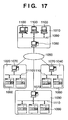
- Fig. 17 shows the overall system cut out at a given angle.
- reference numeral 1010 denotes a business office of a vendor (apparatus supply manufacturer) which provides a semiconductor device manufacturing apparatus.
- the manufacturing apparatus are semiconductor manufacturing apparatuses for various processes used in a semiconductor manufacturing factory, such as pre-process apparatuses (lithography apparatus including an exposure apparatus, resist processing apparatus, and etching apparatus, annealing apparatus, film formation apparatus, planarization apparatus, and the like) and post-process apparatuses (assembly apparatus, inspection apparatus, and the like).
- the business office 1010 comprises a host management system 1080 for providing a maintenance database for the manufacturing apparatus, a plurality of operation terminal computers 1100, and a LAN (Local Area Network) 1090 which connects the host management system 1080 and computers 1100 to construct an intranet.
- the host management system 1080 has a gateway for connecting the LAN 1090 to Internet 1050 as an external network of the business office, and a security function for limiting external accesses.
- Reference numerals 1020 to 1040 denote manufacturing factories of the semiconductor manufacturer as users of manufacturing apparatuses.
- the manufacturing factories 1020 to 1040 may belong to different manufacturers or the same manufacturer (pre-process factory, post-process factory, and the like).
- Each of the factories 1020 to 1040 is equipped with a plurality of manufacturing apparatuses 1060, a LAN (Local Area Network) 1110 which connects these apparatuses 1060 to construct an intranet, and a host management system 1070 serving as a monitoring apparatus for monitoring the operation status of each manufacturing apparatus 1060.
- the host management system 1070 in each of the factories 1020 to 1040 has a gateway for connecting the LAN 1110 in the factory to the Internet 1050 as an external network of the factory.
- Each factory can.access the host management system 1080 of the vendor 1010 from the LAN 1110 via the Internet 1050.
- the security function of the host management system 1080 authorizes access of only a limited user to the host management system 1080.
- the factory notifies the vender via the Internet 1050 of status information (e.g., the symptom of a manufacturing apparatus in trouble) representing the operation status of each manufacturing apparatus 1060.
- the vender transmits, to the factory, response information (e.g., information designating a remedy against the trouble, or remedy software or data) corresponding to the notification, or maintenance information such as the latest software or help information.
- Data communication between the factories 1020 to 1040 and the vender 1010 and data communication via the LAN 1110 in each factory typically adopt a communication protocol (TCP/IP) generally used in the Internet.
- TCP/IP communication protocol
- a dedicated-line network e.g., ISDN
- the user constructs a database in addition to one provided by the vendor and sets the database on an external network and that the host management system authorizes access to the database from a plurality of user factories.
- Fig. 18 is a view showing the concept of the overall system of this embodiment that is cut out at a different angle from Fig. 17 .
- a plurality of user factories having manufacturing apparatuses and the management system of the manufacturing apparatus vendor are connected via an external network, and production management of each factory or information of at least one manufacturing apparatus is communicated via the external network.
- a factory having a plurality of manufacturing apparatuses of a plurality of vendors, and the management systems of the vendors for these manufacturing apparatuses are connected via the external network of the factory, and maintenance information of each manufacturing apparatus is communicated.
- Fig. 18 a factory having a plurality of manufacturing apparatuses of a plurality of vendors, and the management systems of the vendors for these manufacturing apparatuses are connected via the external network of the factory, and maintenance information of each manufacturing apparatus is communicated.
- reference numeral 2010 denotes a manufacturing factory of a manufacturing apparatus user (semiconductor device manufacturer) where manufacturing apparatuses for various processes, e.g., an exposure apparatus 2020, resist processing apparatus 2030, and film formation apparatus 2040 are installed in the manufacturing line of the factory.
- Fig. 18 shows only one manufacturing factory 2010, but a plurality of factories are networked in practice.
- the respective apparatuses in the factory are connected to a LAN 2060 to construct an intranet, and a host management system 2050 manages the operation of the manufacturing line.
- the business offices of vendors such as an exposure apparatus manufacturer 2100, resist processing apparatus manufacturer 2200, and film formation apparatus manufacturer 2300 comprise host management systems 2110, 2210, and 2310 for executing remote maintenance for the supplied apparatuses.
- Each host management system has a maintenance database and a gateway for an external network, as described above.
- the host management system 2050 for managing the apparatuses in the manufacturing factory of the user, and the management systems 2110, 2210, and 2310 of the vendors for the respective apparatuses are connected via the Internet or dedicated-line network serving as an external network 2000. If a trouble occurs in any one of a series of manufacturing apparatuses along the manufacturing line in this system, the operation of the manufacturing line stops. This trouble can be quickly solved by remote maintenance from the vendor of the apparatus in trouble via the Internet 2000. This can minimize the stop of the manufacturing line.
- Each manufacturing apparatus in the semiconductor manufacturing factory comprises a display, a network interface, and a computer for executing network access software and apparatus operating software which are stored in a storage device.
- the storage device is a built-in memory, hard disk, or network file server.
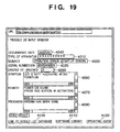
- the network access software includes a dedicated or general-purpose web browser, and provides a user interface having a window as shown in Fig. 19 on the display. While referring to this window, the operator who manages manufacturing apparatuses in each factory inputs, in input items on the windows, pieces of information such as the type of manufacturing apparatus (4010), serial number (4020), subject of trouble (4030), occurrence date (4040), degree of urgency (4050), symptom (4060), remedy (4070), and progress (4080).
- the pieces of input information are transmitted to the maintenance database via the Internet, and appropriate maintenance information is sent back from the maintenance database and displayed on the display.
- the user interface provided by the web browser realizes hyperlink functions (4100 to 4120), as shown in Fig. 19 . This allows the operator to access detailed information of each item, receive the latest-version software to be used for a manufacturing apparatus from a software library provided by a vendor, and receive an operation guide (help information) as a reference for the operator in the factory.
- Fig. 20 shows the flow of the whole manufacturing process of the semiconductor device.
- step 1 circuit design
- step 2 creation of exposure control data
- step 3 wafer manufacture
- step 4 wafer process
- an actual circuit is formed on the wafer by lithography using a prepared mask and the wafer.
- Step 5 is the step of forming a semiconductor chip by using the wafer manufactured in step 4, and includes an assembly process (dicing and bonding) and packaging process (chip encapsulation).
- step 6 inspections such as the operation confirmation test and durability test of the semiconductor device manufactured in step 5 are conducted.
- the semiconductor device is completed and shipped (step 7).
- the pre-process and post-process may be performed in separate dedicated factories. In this case, maintenance is done for each of the factories by the above-described remote maintenance system. Information for production management and apparatus maintenance may be communicated between the pre-process factory and the post-process factory via the Internet or dedicated-line network.
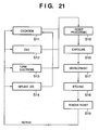
- Fig. 21 shows the detailed flow of the wafer process.
- step 11 oxidation
- step 12 CVD
- step 13 electrode formation
- step 14 ion implantation
- step 15 resist processing
- step 16 exposure
- step 17 developing
- step 18 etching
- the resist is etched except for the developed resist image.
- step 19 resist removal
- step 19 resist removal
- steps 19 resist removal
- steps 19 are repeated to form multiple circuit patterns on the wafer.
- a manufacturing apparatus used in each step undergoes maintenance by the remote maintenance system, which prevents a trouble in advance. Even if a trouble occurs, the manufacturing apparatus can be quickly recovered. The productivity of the semiconductor device can be increased in comparison with the prior art.
- the present invention can provide an electron optical system array which realizes various conditions such as downsizing, high precision, and high reliability at high level.
- the present invention can also provide a high-precision exposure apparatus using the electron optical system array, a high-productivity device manufacturing method, a semiconductor device production factory, and the like.
Claims (17)
- Ladungsträgerteilchenoptische Anordnung mit einer Vielzahl von Ladungsträgerteilchenlinsen, mit:einer Vielzahl von Elektroden (1 bis 3), die entlang von Wegen einer Vielzahl von Ladungsträgerteilchenstrahlen angeordnet sind, wobei jede der Vielzahl von Elektroden (1 bis 3) eine Membran (1A, 2A, 3A), in der eine Vielzahl von Öffnungen (105, 207) auf den Wegen der Vielzahl von Ladungsträgerteilchenstrahlen ausgebildet ist, und einen Trägerabschnitt (1B, 2B, 3B) aufweist, der die Membran (1A, 2A, 3A) trägt, und wobei zumindest zwei der Vielzahl von Elektroden (1 bis 3) angeordnet sind, um einen ineinander geschachtelten Aufbau zu bilden, undeinem Basiselement (4), wobeidas Basiselement (4) eine erste Oberfläche aufweist, in der ein Durchgangsloch (303) derart ausgebildet ist, dass die Vielzahl von Ladungsträgerteilchenstrahlen durch das Durchgangsloch (303) hindurchgeht,
dadurch gekennzeichnet, dassjeder der Trägerabschnitte (1B, 2B, 3B) der zumindest zwei Elektroden (1 bis 3) auf der ersten Oberfläche des Basiselements (4) benachbart zueinander angeordnet ist und der Trägerabschnitt (2B) einer der zumindest zwei Elektroden innerhalb des Trägerabschnitts (1B) einer anderen der zumindest zwei Elektroden angeordnet ist. - Anordnung nach Anspruch 1, wobei alle der Vielzahl von Elektroden (1 bis 3) angeordnet sind, um den ineinander geschachtelten Aufbau zu bilden.
- Anordnung nach Anspruch 2, wobei die Trägerabschnitte (1B, 2B, 3B) aller der Vielzahl von Elektroden (1 bis 3) durch die erste Oberfläche des Basiselements (4) getragen werden.
- Anordnung nach Anspruch 1, wobei jeder von zumindest zwei Sätzen der Vielzahl von Elektroden (1 bis 3) angeordnet ist, um die ineinander geschachtelten Aufbauten zu bilden.
- Anordnung nach Anspruch 4, wobei
das Basiselement (4) einen der zumindest zwei Sätze durch die erste Oberfläche trägt und den anderen der zumindest zwei Sätze durch eine zweite Oberfläche des Basiselements (4) trägt. - Anordnung nach Anspruch 4, ferner mit einem anderen Basiselement (24), das einen der zumindest zwei Sätze trägt.
- Anordnung nach Anspruch 6, ferner mit einem Kopplungsabschnitt (26), der die zumindest zwei Sätze koppelt.
- Anordnung nach Anspruch 1, wobei
die Trägerabschnitte (1B, 2B, 3B) von zumindest zwei Elektroden (1 bis 3) hohle Abschnitte (106) aufweisen, und
eine der zumindest zwei Elektroden (1 bis 3) innerhalb des hohlen Abschnitts (106) der anderen der zumindest zwei Elektroden (1 bis 3) angeordnet ist. - Anordnung nach Anspruch 1, wobei eine der Vielzahl von Elektroden (1 bis 3) mit Ausnahme der zumindest zwei Elektroden einer Elektrode gegenüberliegt, die von den zumindest zwei Elektroden von dem Basiselement (4) am weitesten entfernt ist.
- Anordnung nach Anspruch 9, wobei der Trägerabschnitt (1B, 2B, 3B) der einen der Vielzahl von Elektroden mit Ausnahme der zumindest zwei Elektroden in seiner Größe kleiner als der Trägerabschnitt (1B, 2B, 3B) der Elektrode ist, die von dem Basiselement am weitesten entfernt angeordnet ist.
- Anordnung nach Anspruch 1, wobei die Vielzahl von Elektroden angeordnet ist, um zu verhindern, dass die Membranen (1A, 2A, 3A) der Vielzahl von Elektroden (1 bis 3) einander kontaktieren.
- Anordnung nach Anspruch 1, wobei zumindest eine der Vielzahl von Elektroden (1 bis 3) in Kolonneneinheiten aufgeteilt ist, die jede eine Vielzahl von Öffnungen (105) umfasst.
- Anordnung nach Anspruch 1, wobei
zumindest eine der Vielzahl von Elektroden (1 bis 3) eine Elektrode zur Bildung eines elektrischen Felds ist, das auf einen Ladungsträgerteilchenstrahl wirkt, und
zumindest eine andere der Vielzahl von Elektroden eine Abschirmungselektrode (406) ist. - Verfahren zur Herstellung einer ladungsträgerteilchenoptischen Anordnung nach Anspruch 1, mit:einem Vorbereitungsschritt zur Vorbereitung der Vielzahl von Elektroden (1 bis 3),einem Schritt zum Vorbereiten des Basiselements (4), undeinem Fixierschritt zum Fixieren der Trägerabschnitte (1B, 2B, 3B) der zumindest zwei Elektroden auf dem Basiselement (4), um den ineinander geschachtelten Aufbau zu bilden.
- Verfahren nach Anspruch 14, wobei die Vielzahl von Elektroden (1 bis 3) in dem Elektrodenvorbereitungsschritt unter Verwendung eines Beschichtens hergestellt wird.
- Ladungsträgerteilchenstrahl-Belichtungsgerät mit:einer Ladungsträgerteilchenstrahlquelle (501) zum Emittieren eines Ladungsträgerteilchenstrahls,einer ladungsträgerteilchenoptischen Anordnung (502, 503) nach einem der Ansprüche 1 bis 13, die eingerichtet ist, eine Vielzahl von Zwischenbildern der Ladungsträgerteilchenstrahlquelle (501) durch die Vielzahl von Ladungsträgerteilchenlinsen zu bilden, undeinem ladungsträgerteilchenoptischen Projektionssystem (504) zum Projizieren der Vielzahl von Zwischenbildern, die durch die ladungsträgerteilchenoptische Anordnung gebildet werden, auf ein Substrat (505).
- Verfahren zur Herstellung einer Vorrichtung, mit:einem Belichten eines Halbleitersubstrats mit einem Ladungsträgerteilchenstrahl unter Verwendung eines Ladungsträgerteilchenstrahl-Belichtungsgeräts nach Anspruch 16,Entwickeln des belichteten Substrats, undVerarbeiten des entwickelten Substrats, um die Vorrichtung herzustellen.
Applications Claiming Priority (4)
| Application Number | Priority Date | Filing Date | Title |
|---|---|---|---|
| JP2000097067 | 2000-03-31 | ||
| JP2000097067 | 2000-03-31 | ||
| JP2001074736 | 2001-03-15 | ||
| JP2001074736A JP4947841B2 (ja) | 2000-03-31 | 2001-03-15 | 荷電粒子線露光装置 |
Publications (3)
| Publication Number | Publication Date |
|---|---|
| EP1139384A2 EP1139384A2 (de) | 2001-10-04 |
| EP1139384A3 EP1139384A3 (de) | 2007-08-29 |
| EP1139384B1 true EP1139384B1 (de) | 2009-09-23 |
Family
ID=26589082
Family Applications (1)
| Application Number | Title | Priority Date | Filing Date |
|---|---|---|---|
| EP01303029A Expired - Lifetime EP1139384B1 (de) | 2000-03-31 | 2001-03-30 | Elektronenoptische Anordnung, Verfahren zur Herstellung derselben, Ladungsträgerteilchenstrahl-Belichtungsgerät und Verfahren zur Herstellung der zugehörigen Vorrichtung |
Country Status (5)
| Country | Link |
|---|---|
| US (1) | US6872950B2 (de) |
| EP (1) | EP1139384B1 (de) |
| JP (1) | JP4947841B2 (de) |
| AT (1) | ATE443922T1 (de) |
| DE (1) | DE60139968D1 (de) |
Families Citing this family (51)
| Publication number | Priority date | Publication date | Assignee | Title |
|---|---|---|---|---|
| JP3996267B2 (ja) * | 1998-05-12 | 2007-10-24 | エルピーダメモリ株式会社 | 半導体記憶装置 |
| JP3763446B2 (ja) * | 1999-10-18 | 2006-04-05 | キヤノン株式会社 | 静電レンズ、電子ビーム描画装置、荷電ビーム応用装置、および、デバイス製造方法 |
| JP4585661B2 (ja) * | 2000-03-31 | 2010-11-24 | キヤノン株式会社 | 電子光学系アレイ、荷電粒子線露光装置およびデバイス製造方法 |
| JP2001284230A (ja) | 2000-03-31 | 2001-10-12 | Canon Inc | 電子光学系アレイ、これを用いた荷電粒子線露光装置ならびにデバイス製造方法 |
| GB2412494B (en) * | 2002-01-17 | 2006-02-01 | Ims Nanofabrication Gmbh | Maskless particle-beam system for exposing a pattern on a substrate |
| US6768125B2 (en) * | 2002-01-17 | 2004-07-27 | Ims Nanofabrication, Gmbh | Maskless particle-beam system for exposing a pattern on a substrate |
| JP2004134388A (ja) * | 2002-08-13 | 2004-04-30 | Leo Elektronenmikroskopie Gmbh | 粒子光学装置、電子顕微鏡システムおよび電子リソグラフィーシステム |
| DE10237297A1 (de) * | 2002-08-14 | 2004-03-11 | Leo Elektronenmikroskopie Gmbh | Teilchenoptische Vorrichtung, Elektronenmikroskopiesystem und Lithogrphiesystem |
| US6953938B2 (en) * | 2002-10-03 | 2005-10-11 | Canon Kabushiki Kaisha | Deflector, method of manufacturing deflector, and charged particle beam exposure apparatus |
| JP2004282038A (ja) | 2003-02-28 | 2004-10-07 | Canon Inc | 偏向器、偏向器を製造する方法、偏向器を適用した荷電粒子線露光装置 |
| JP4459568B2 (ja) * | 2003-08-06 | 2010-04-28 | キヤノン株式会社 | マルチ荷電ビームレンズおよびそれを用いた荷電ビーム露光装置 |
| EP2579274A1 (de) | 2003-09-05 | 2013-04-10 | Carl Zeiss SMT GmbH | Optische Partikelsysteme und Anordnungen und optische Partikelkomponenten für solche Systeme und Anordnungen |
| GB2408383B (en) * | 2003-10-28 | 2006-05-10 | Ims Nanofabrication Gmbh | Pattern-definition device for maskless particle-beam exposure apparatus |
| JP2007518223A (ja) * | 2003-12-30 | 2007-07-05 | コミツサリア タ レネルジー アトミーク | 発散制御機能を有したハイブリッド型マルチビーム電子放出デバイス |
| EP1557866B1 (de) * | 2004-01-21 | 2011-03-16 | ICT Integrated Circuit Testing Gesellschaft für Halbleiterprüftechnik mbH | Strahlenoptische Komponente mit einer teilchenoptischen Linse |
| WO2005112103A2 (en) * | 2004-05-07 | 2005-11-24 | Stillwater Scientific Instruments | Microfabricated miniature grids |
| JP4559137B2 (ja) * | 2004-06-30 | 2010-10-06 | キヤノン株式会社 | 真空機器の製造装置及び製造方法 |
| US7468507B2 (en) * | 2005-01-26 | 2008-12-23 | Applied Materials, Israel, Ltd. | Optical spot grid array scanning system |
| US7468506B2 (en) * | 2005-01-26 | 2008-12-23 | Applied Materials, Israel, Ltd. | Spot grid array scanning system |
| US8304749B2 (en) | 2005-02-11 | 2012-11-06 | Ims Nanofabrication Ag | Charged-particle exposure apparatus with electrostatic zone plate |
| JP2007231324A (ja) * | 2006-02-28 | 2007-09-13 | Canon Inc | マルチ荷電ビーム加工装置 |
| WO2007103375A2 (en) * | 2006-03-06 | 2007-09-13 | Stillwater Scientific Instruments | Gating grid and method of manufacture |
| JP2008066359A (ja) * | 2006-09-05 | 2008-03-21 | Canon Inc | 荷電ビームレンズアレイ、露光装置及びデバイス製造方法 |
| EP2019415B1 (de) | 2007-07-24 | 2016-05-11 | IMS Nanofabrication AG | Mehrfachstrahlquelle |
| TWI492261B (zh) * | 2009-10-09 | 2015-07-11 | Mapper Lithography Ip Bv | 提高完整性的投影透鏡組件 |
| US8362441B2 (en) | 2009-10-09 | 2013-01-29 | Mapper Lithography Ip B.V. | Enhanced integrity projection lens assembly |
| US8987679B2 (en) | 2009-10-09 | 2015-03-24 | Mapper Lithography Ip B.V. | Enhanced integrity projection lens assembly |
| NL2003619C2 (en) * | 2009-10-09 | 2011-04-12 | Mapper Lithography Ip Bv | Projection lens assembly. |
| JP5669636B2 (ja) * | 2011-03-15 | 2015-02-12 | キヤノン株式会社 | 荷電粒子線レンズおよびそれを用いた露光装置 |
| JP2012195095A (ja) * | 2011-03-15 | 2012-10-11 | Canon Inc | 荷電粒子線レンズの製造方法 |
| JP2013004216A (ja) * | 2011-06-14 | 2013-01-07 | Canon Inc | 荷電粒子線レンズ |
| US8933425B1 (en) * | 2011-11-02 | 2015-01-13 | Kla-Tencor Corporation | Apparatus and methods for aberration correction in electron beam based system |
| JP2013168396A (ja) * | 2012-02-14 | 2013-08-29 | Canon Inc | 静電型の荷電粒子線レンズ及び荷電粒子線装置 |
| JP2013239667A (ja) * | 2012-05-17 | 2013-11-28 | Canon Inc | 荷電粒子線静電レンズにおける電極とその製造方法、荷電粒子線静電レンズ、及び荷電粒子線露光装置 |
| JP2014007013A (ja) * | 2012-06-22 | 2014-01-16 | Canon Inc | 静電レンズアレイ、マルチ荷電粒子光学系、及びフォーカス調整方法 |
| US8890092B2 (en) * | 2013-01-28 | 2014-11-18 | Industry—University Cooperation Foundation Sunmoon University | Multi-particle beam column having an electrode layer including an eccentric aperture |
| DE102014018555B3 (de) * | 2014-12-15 | 2016-03-03 | MAX-PLANCK-Gesellschaft zur Förderung der Wissenschaften e.V. | Elektrodenträgereinrichtung und elektronen-optische Linse für elektrisch geladene Teilchen sowie deren Verwendung |
| DE102015202172B4 (de) | 2015-02-06 | 2017-01-19 | Carl Zeiss Microscopy Gmbh | Teilchenstrahlsystem und Verfahren zur teilchenoptischen Untersuchung eines Objekts |
| JP6662685B2 (ja) * | 2016-03-31 | 2020-03-11 | Jx金属株式会社 | めっき層を有するチタン銅箔 |
| JP6772962B2 (ja) * | 2017-06-02 | 2020-10-21 | 株式会社ニューフレアテクノロジー | マルチ荷電粒子ビーム描画装置及びマルチ荷電粒子ビーム描画方法 |
| KR102401179B1 (ko) * | 2017-12-12 | 2022-05-24 | 삼성전자주식회사 | 전자빔 장치의 어퍼처 시스템, 전자빔 노광 장치 및 전자빔 노광 장치 시스템 |
| DE102018202421B3 (de) | 2018-02-16 | 2019-07-11 | Carl Zeiss Microscopy Gmbh | Vielstrahl-Teilchenstrahlsystem |
| DE102018202428B3 (de) | 2018-02-16 | 2019-05-09 | Carl Zeiss Microscopy Gmbh | Vielstrahl-Teilchenmikroskop |
| WO2019166331A2 (en) | 2018-02-27 | 2019-09-06 | Carl Zeiss Microscopy Gmbh | Charged particle beam system and method |
| US10811215B2 (en) | 2018-05-21 | 2020-10-20 | Carl Zeiss Multisem Gmbh | Charged particle beam system |
| DE102018007455B4 (de) | 2018-09-21 | 2020-07-09 | Carl Zeiss Multisem Gmbh | Verfahren zum Detektorabgleich bei der Abbildung von Objekten mittels eines Mehrstrahl-Teilchenmikroskops, System sowie Computerprogrammprodukt |
| DE102018007652B4 (de) | 2018-09-27 | 2021-03-25 | Carl Zeiss Multisem Gmbh | Teilchenstrahl-System sowie Verfahren zur Stromregulierung von Einzel-Teilchenstrahlen |
| DE102018124044B3 (de) | 2018-09-28 | 2020-02-06 | Carl Zeiss Microscopy Gmbh | Verfahren zum Betreiben eines Vielstrahl-Teilchenstrahlmikroskops und Vielstrahl-Teilchenstrahlsystem |
| US11145485B2 (en) * | 2018-12-26 | 2021-10-12 | Nuflare Technology, Inc. | Multiple electron beams irradiation apparatus |
| CN111477530B (zh) | 2019-01-24 | 2023-05-05 | 卡尔蔡司MultiSEM有限责任公司 | 利用多束粒子显微镜对3d样本成像的方法 |
| TWI743626B (zh) | 2019-01-24 | 2021-10-21 | 德商卡爾蔡司多重掃描電子顯微鏡有限公司 | 包含多束粒子顯微鏡的系統、對3d樣本逐層成像之方法及電腦程式產品 |
Family Cites Families (69)
| Publication number | Priority date | Publication date | Assignee | Title |
|---|---|---|---|---|
| US3484645A (en) * | 1967-03-06 | 1969-12-16 | Us Army | Non-intercepting grid structure for an electron tube |
| US3491236A (en) * | 1967-09-28 | 1970-01-20 | Gen Electric | Electron beam fabrication of microelectronic circuit patterns |
| US3534219A (en) * | 1969-01-03 | 1970-10-13 | Gen Electric | Cascaded electron optical system |
| DE2109450A1 (de) * | 1970-11-30 | 1972-07-06 | Tokyo Shibaura Electric Co | Kathodenstrahlröhre mit doppelter Ablenkung in einer Richtung |
| US4200794A (en) * | 1978-11-08 | 1980-04-29 | Control Data Corporation | Micro lens array and micro deflector assembly for fly's eye electron beam tubes using silicon components and techniques of fabrication and assembly |
| SE421832B (sv) | 1979-04-18 | 1982-02-01 | Pharos Ab | Anordning for att registrera topografin hos den chargerade massan i en masugn |
| US4419182A (en) | 1981-02-27 | 1983-12-06 | Veeco Instruments Inc. | Method of fabricating screen lens array plates |
| US4354111A (en) | 1981-03-10 | 1982-10-12 | Veeco Instruments Incorporated | Screen lens array system |
| US4419580A (en) | 1981-06-26 | 1983-12-06 | Control Data Corporation | Electron beam array alignment means |
| US4607167A (en) | 1982-10-19 | 1986-08-19 | Varian Associates, Inc. | Charged particle beam lithography machine incorporating localized vacuum envelope |
| US4569033A (en) | 1983-06-14 | 1986-02-04 | The United States Of America As Represented By The Secretary Of The Navy | Optical matrix-matrix multiplier based on outer product decomposition |
| JPS6251649U (de) * | 1985-09-18 | 1987-03-31 | ||
| US4742234A (en) | 1985-09-27 | 1988-05-03 | American Telephone And Telegraph Company, At&T Bell Laboratories | Charged-particle-beam lithography |
| JPS63236251A (ja) * | 1987-03-23 | 1988-10-03 | Jeol Ltd | 電子ビ−ム−イオンビ−ム複合装置 |
| JP2523931B2 (ja) | 1990-04-16 | 1996-08-14 | 富士通株式会社 | ブランキングアパ―チャアレ―の製造方法 |
| JP2837515B2 (ja) | 1990-06-20 | 1998-12-16 | 富士通株式会社 | 電子ビーム露光装置 |
| US5121234A (en) | 1990-10-29 | 1992-06-09 | Honeywell Incorporated | Dichroic liquid crystal display with integral electroluminescent backlighting |
| JPH04179116A (ja) * | 1990-11-09 | 1992-06-25 | Hitachi Ltd | 荷電粒子線装置 |
| DE69226553T2 (de) | 1991-03-13 | 1998-12-24 | Fujitsu Ltd | Vorrichtung und Verfahren zur Belichtung mittels Ladungsträgerstrahlen |
| US6184850B1 (en) | 1991-09-04 | 2001-02-06 | Canon Kabushiki Kaisha | Image display apparatus with backlit display and method of driving the same |
| JPH0644093A (ja) | 1992-04-01 | 1994-02-18 | Nec Corp | 二重化装置切替方式 |
| JPH0636730A (ja) * | 1992-07-15 | 1994-02-10 | Fujitsu Ltd | 荷電ビーム装置 |
| WO1994011896A1 (en) | 1992-11-06 | 1994-05-26 | Mitsubishi Denki Kabushiki Kaisha | Image display |
| US5324930A (en) | 1993-04-08 | 1994-06-28 | Eastman Kodak Company | Lens array for photodiode device with an aperture having a lens region and a non-lens region |
| US5617131A (en) | 1993-10-28 | 1997-04-01 | Kyocera Corporation | Image device having a spacer with image arrays disposed in holes thereof |
| JPH07122468A (ja) * | 1993-10-28 | 1995-05-12 | Mitsubishi Electric Corp | 電子ビーム描画装置およびその装置を用いた描画方法 |
| US5534311A (en) | 1995-05-31 | 1996-07-09 | The United States Of America As Represented By The Secretary Of The Navy | Production of structures by electrostatically-focused deposition |
| US5942761A (en) | 1995-06-07 | 1999-08-24 | Tuli; Raja Singh | Enhancement methods and devices for reading a fingerprint image |
| JPH097538A (ja) * | 1995-06-26 | 1997-01-10 | Nippon Telegr & Teleph Corp <Ntt> | 荷電ビーム描画装置 |
| JP2785788B2 (ja) | 1996-01-19 | 1998-08-13 | 日本電気株式会社 | 一括マスク搭載ホルダ構造 |
| DE69738276T2 (de) | 1996-03-04 | 2008-04-03 | Canon K.K. | Elektronenstrahl-Belichtungsgerät, Belichtungsverfahren und Verfahren zur Erzeugung eines Objekts |
| US5621216A (en) * | 1996-04-26 | 1997-04-15 | International Business Machines Corporation | Hardware/software implementation for multipass E-beam mask writing |
| JP3796317B2 (ja) | 1996-06-12 | 2006-07-12 | キヤノン株式会社 | 電子ビーム露光方法及びそれを用いたデバイス製造方法 |
| US5929454A (en) | 1996-06-12 | 1999-07-27 | Canon Kabushiki Kaisha | Position detection apparatus, electron beam exposure apparatus, and methods associated with them |
| JP3927620B2 (ja) | 1996-06-12 | 2007-06-13 | キヤノン株式会社 | 電子ビーム露光方法及びそれを用いたデバイス製造方法 |
| US5981954A (en) | 1997-01-16 | 1999-11-09 | Canon Kabushiki Kaisha | Electron beam exposure apparatus |
| JPH10214779A (ja) | 1997-01-31 | 1998-08-11 | Canon Inc | 電子ビーム露光方法及び該方法を用いたデバイス製造方法 |
| US6107636A (en) | 1997-02-07 | 2000-08-22 | Canon Kabushiki Kaisha | Electron beam exposure apparatus and its control method |
| JP3062995B2 (ja) | 1997-03-27 | 2000-07-12 | セイコーインスツルメンツ株式会社 | 電子時計 |
| US5886432A (en) | 1997-04-28 | 1999-03-23 | Ultratech Stepper, Inc. | Magnetically-positioned X-Y stage having six-degrees of freedom |
| US6274877B1 (en) | 1997-05-08 | 2001-08-14 | Canon Kabushiki Kaisha | Electron beam exposure apparatus |
| JP3478058B2 (ja) | 1997-05-30 | 2003-12-10 | 株式会社日立製作所 | 荷電粒子線描画装置 |
| US6104035A (en) | 1997-06-02 | 2000-08-15 | Canon Kabushiki Kaisha | Electron-beam exposure apparatus and method |
| JP3787417B2 (ja) | 1997-06-11 | 2006-06-21 | キヤノン株式会社 | 電子ビーム露光方法及び電子ビーム露光装置 |
| JPH1187206A (ja) * | 1997-09-02 | 1999-03-30 | Canon Inc | 電子ビーム露光装置及び該装置を用いたデバイス製造方法 |
| KR19990062942A (ko) | 1997-12-10 | 1999-07-26 | 히로시 오우라 | 전하 입자 빔 노출 장치 |
| US6381072B1 (en) | 1998-01-23 | 2002-04-30 | Proxemics | Lenslet array systems and methods |
| US6014200A (en) | 1998-02-24 | 2000-01-11 | Nikon Corporation | High throughput electron beam lithography system |
| JP2000030647A (ja) | 1998-07-10 | 2000-01-28 | Advantest Corp | 荷電粒子ビーム露光装置 |
| US6137103A (en) | 1998-07-31 | 2000-10-24 | Lucent Technologies | Opto-mechanical components |
| JP2000181643A (ja) | 1998-12-11 | 2000-06-30 | Canon Inc | 画像形成装置及び画像形成方法 |
| JP4410871B2 (ja) | 1999-03-25 | 2010-02-03 | キヤノン株式会社 | 荷電粒子線露光装置及び該装置を用いたデバイス製造方法 |
| JP2001052998A (ja) * | 1999-06-03 | 2001-02-23 | Advantest Corp | 荷電粒子ビーム結像方法、荷電粒子ビーム結像装置及び荷電粒子ビーム露光装置 |
| JP2001076990A (ja) | 1999-08-31 | 2001-03-23 | Canon Inc | 荷電粒子線露光装置及びその制御方法 |
| US6693684B2 (en) | 1999-09-15 | 2004-02-17 | Rainbow Displays, Inc. | Construction of large, robust, monolithic and monolithic-like, AMLCD displays with wide view angle |
| JP3763446B2 (ja) | 1999-10-18 | 2006-04-05 | キヤノン株式会社 | 静電レンズ、電子ビーム描画装置、荷電ビーム応用装置、および、デバイス製造方法 |
| JP2001126651A (ja) | 1999-10-22 | 2001-05-11 | Hitachi Ltd | 電子ビーム描画装置 |
| JP2001168017A (ja) | 1999-12-13 | 2001-06-22 | Canon Inc | 荷電粒子線露光装置、荷電粒子線露光方法及び制御データの決定方法、該方法を適用したデバイスの製造方法。 |
| JP2001168016A (ja) | 1999-12-13 | 2001-06-22 | Canon Inc | 荷電粒子線露光装置と露光システム及びそれらの制御方法及びデバイス製造方法 |
| US6566644B1 (en) | 1999-12-15 | 2003-05-20 | Litton Systems, Inc. | Optical fiber sorter system and method |
| US6566664B2 (en) | 2000-03-17 | 2003-05-20 | Canon Kabushiki Kaisha | Charged-particle beam exposure apparatus and device manufacturing method |
| JP4585661B2 (ja) | 2000-03-31 | 2010-11-24 | キヤノン株式会社 | 電子光学系アレイ、荷電粒子線露光装置およびデバイス製造方法 |
| JP2001284230A (ja) | 2000-03-31 | 2001-10-12 | Canon Inc | 電子光学系アレイ、これを用いた荷電粒子線露光装置ならびにデバイス製造方法 |
| JP2001283756A (ja) | 2000-03-31 | 2001-10-12 | Canon Inc | 電子光学系アレイ、これを用いた荷電粒子線露光装置ならびにデバイス製造方法 |
| JP4947842B2 (ja) | 2000-03-31 | 2012-06-06 | キヤノン株式会社 | 荷電粒子線露光装置 |
| JP3728217B2 (ja) | 2000-04-27 | 2005-12-21 | キヤノン株式会社 | 荷電粒子線露光装置およびデバイス製造方法 |
| JP4647820B2 (ja) | 2001-04-23 | 2011-03-09 | キヤノン株式会社 | 荷電粒子線描画装置、および、デバイスの製造方法 |
| JP4756776B2 (ja) | 2001-05-25 | 2011-08-24 | キヤノン株式会社 | 荷電粒子線露光装置、荷電粒子線露光方法およびデバイス製造方法 |
| EP2434522B8 (de) | 2002-07-16 | 2014-07-23 | Canon Kabushiki Kaisha | Linse für einen Ladungsträger-Vielfachstrahl, Ladungsträgerstrahlbelichtungsapparatur mit einer solchen Linse und entsprechendes Herstellungsverfahren |
-
2001
- 2001-03-15 JP JP2001074736A patent/JP4947841B2/ja not_active Expired - Fee Related
- 2001-03-29 US US09/819,669 patent/US6872950B2/en not_active Expired - Fee Related
- 2001-03-30 AT AT01303029T patent/ATE443922T1/de not_active IP Right Cessation
- 2001-03-30 EP EP01303029A patent/EP1139384B1/de not_active Expired - Lifetime
- 2001-03-30 DE DE60139968T patent/DE60139968D1/de not_active Expired - Lifetime
Also Published As
| Publication number | Publication date |
|---|---|
| DE60139968D1 (de) | 2009-11-05 |
| ATE443922T1 (de) | 2009-10-15 |
| EP1139384A3 (de) | 2007-08-29 |
| EP1139384A2 (de) | 2001-10-04 |
| JP4947841B2 (ja) | 2012-06-06 |
| US20010054690A1 (en) | 2001-12-27 |
| JP2001345260A (ja) | 2001-12-14 |
| US6872950B2 (en) | 2005-03-29 |
Similar Documents
| Publication | Publication Date | Title |
|---|---|---|
| EP1139384B1 (de) | Elektronenoptische Anordnung, Verfahren zur Herstellung derselben, Ladungsträgerteilchenstrahl-Belichtungsgerät und Verfahren zur Herstellung der zugehörigen Vorrichtung | |
| US6965153B1 (en) | Electrooptic system array, charged-particle beam exposure apparatus using the same, and device manufacturing method | |
| US6903345B2 (en) | Electron optical system, charged-particle beam exposure apparatus using the same, and device manufacturing method | |
| US6872951B2 (en) | Electron optical system array, charged-particle beam exposure apparatus using the same, and device manufacturing method | |
| US6872952B2 (en) | Electron optical system array, method of manufacturing the same, charged-particle beam exposure apparatus, and device manufacturing method | |
| US7060984B2 (en) | Multi-charged beam lens and charged beam exposure apparatus using the same | |
| KR100520639B1 (ko) | 대전 입자선 노광장치 및 디바이스제조방법 | |
| US20030066974A1 (en) | Charged-particle beam exposure apparatus and device manufacturing method | |
| JPH09330871A (ja) | 電子ビーム露光システム及びそれを用いたデバイス製造方法 | |
| JP2008027686A (ja) | 偏向器アレイ、露光装置およびデバイス製造方法 | |
| JP2000138165A (ja) | 荷電粒子描画方法及び荷電粒子描画装置 | |
| JP2007266525A (ja) | 荷電粒子線レンズアレイ、該荷電粒子線レンズアレイを用いた荷電粒子線露光装置 | |
| JP2001283755A (ja) | 電子光学系アレイとこの作製方法、荷電粒子線露光装置ならびにデバイス製造方法 | |
| JP4615816B2 (ja) | 電子レンズ、その電子レンズを用いた荷電粒子線露光装置、デバイス製造方法 | |
| JP2004055166A (ja) | マルチ荷電ビームレンズ及びこれを用いた荷電粒子線露光装置ならびにデバイス製造方法 | |
| JP2001267221A (ja) | 荷電粒子線露光装置及びデバイス製造方法 | |
| JP2006049702A (ja) | 荷電粒子線レンズアレイ、及び該荷電粒子線レンズアレイを用いた荷電粒子線露光装置 | |
| JP2006049703A (ja) | 荷電粒子線レンズアレイ、及び該荷電粒子線レンズアレイを用いた荷電粒子線露光装置 | |
| JP4252813B2 (ja) | 荷電ビーム用レンズ、荷電ビーム露光装置及びデバイス製造方法 | |
| JP2005286346A (ja) | 電子ビーム露光装置及び該電子ビーム露光装置を管理する管理装置 | |
| JP2001313240A (ja) | 接合用部材及び接合方法並びに荷電粒子線描画装置 |
Legal Events
| Date | Code | Title | Description |
|---|---|---|---|
| PUAI | Public reference made under article 153(3) epc to a published international application that has entered the european phase |
Free format text: ORIGINAL CODE: 0009012 |
|
| AK | Designated contracting states |
Kind code of ref document: A2 Designated state(s): AT BE CH CY DE DK ES FI FR GB GR IE IT LI LU MC NL PT SE TR |
|
| AX | Request for extension of the european patent |
Free format text: AL;LT;LV;MK;RO;SI |
|
| PUAL | Search report despatched |
Free format text: ORIGINAL CODE: 0009013 |
|
| AK | Designated contracting states |
Kind code of ref document: A3 Designated state(s): AT BE CH CY DE DK ES FI FR GB GR IE IT LI LU MC NL PT SE TR |
|
| AX | Request for extension of the european patent |
Extension state: AL LT LV MK RO SI |
|
| 17P | Request for examination filed |
Effective date: 20080229 |
|
| AKX | Designation fees paid |
Designated state(s): AT BE CH CY DE DK ES FI FR GB GR IE IT LI LU MC NL PT SE TR |
|
| 17Q | First examination report despatched |
Effective date: 20080411 |
|
| GRAP | Despatch of communication of intention to grant a patent |
Free format text: ORIGINAL CODE: EPIDOSNIGR1 |
|
| RIN1 | Information on inventor provided before grant (corrected) |
Inventor name: SHIMADA, YASUHIRO Inventor name: ONO, HARUHITO Inventor name: YAGI, TAKAYUKI |
|
| GRAS | Grant fee paid |
Free format text: ORIGINAL CODE: EPIDOSNIGR3 |
|
| GRAA | (expected) grant |
Free format text: ORIGINAL CODE: 0009210 |
|
| AK | Designated contracting states |
Kind code of ref document: B1 Designated state(s): AT BE CH CY DE DK ES FI FR GB GR IE IT LI LU MC NL PT SE TR |
|
| REG | Reference to a national code |
Ref country code: GB Ref legal event code: FG4D |
|
| REG | Reference to a national code |
Ref country code: CH Ref legal event code: EP |
|
| REG | Reference to a national code |
Ref country code: IE Ref legal event code: FG4D |
|
| REF | Corresponds to: |
Ref document number: 60139968 Country of ref document: DE Date of ref document: 20091105 Kind code of ref document: P |
|
| PG25 | Lapsed in a contracting state [announced via postgrant information from national office to epo] |
Ref country code: SE Free format text: LAPSE BECAUSE OF FAILURE TO SUBMIT A TRANSLATION OF THE DESCRIPTION OR TO PAY THE FEE WITHIN THE PRESCRIBED TIME-LIMIT Effective date: 20090923 Ref country code: FI Free format text: LAPSE BECAUSE OF FAILURE TO SUBMIT A TRANSLATION OF THE DESCRIPTION OR TO PAY THE FEE WITHIN THE PRESCRIBED TIME-LIMIT Effective date: 20090923 |
|
| PG25 | Lapsed in a contracting state [announced via postgrant information from national office to epo] |
Ref country code: CY Free format text: LAPSE BECAUSE OF FAILURE TO SUBMIT A TRANSLATION OF THE DESCRIPTION OR TO PAY THE FEE WITHIN THE PRESCRIBED TIME-LIMIT Effective date: 20090923 |
|
| PG25 | Lapsed in a contracting state [announced via postgrant information from national office to epo] |
Ref country code: PT Free format text: LAPSE BECAUSE OF FAILURE TO SUBMIT A TRANSLATION OF THE DESCRIPTION OR TO PAY THE FEE WITHIN THE PRESCRIBED TIME-LIMIT Effective date: 20100125 Ref country code: ES Free format text: LAPSE BECAUSE OF FAILURE TO SUBMIT A TRANSLATION OF THE DESCRIPTION OR TO PAY THE FEE WITHIN THE PRESCRIBED TIME-LIMIT Effective date: 20100103 |
|
| PG25 | Lapsed in a contracting state [announced via postgrant information from national office to epo] |
Ref country code: BE Free format text: LAPSE BECAUSE OF FAILURE TO SUBMIT A TRANSLATION OF THE DESCRIPTION OR TO PAY THE FEE WITHIN THE PRESCRIBED TIME-LIMIT Effective date: 20090923 Ref country code: AT Free format text: LAPSE BECAUSE OF FAILURE TO SUBMIT A TRANSLATION OF THE DESCRIPTION OR TO PAY THE FEE WITHIN THE PRESCRIBED TIME-LIMIT Effective date: 20090923 |
|
| PG25 | Lapsed in a contracting state [announced via postgrant information from national office to epo] |
Ref country code: DK Free format text: LAPSE BECAUSE OF FAILURE TO SUBMIT A TRANSLATION OF THE DESCRIPTION OR TO PAY THE FEE WITHIN THE PRESCRIBED TIME-LIMIT Effective date: 20090923 |
|
| PLBE | No opposition filed within time limit |
Free format text: ORIGINAL CODE: 0009261 |
|
| STAA | Information on the status of an ep patent application or granted ep patent |
Free format text: STATUS: NO OPPOSITION FILED WITHIN TIME LIMIT |
|
| 26N | No opposition filed |
Effective date: 20100624 |
|
| PG25 | Lapsed in a contracting state [announced via postgrant information from national office to epo] |
Ref country code: MC Free format text: LAPSE BECAUSE OF NON-PAYMENT OF DUE FEES Effective date: 20100331 Ref country code: GR Free format text: LAPSE BECAUSE OF FAILURE TO SUBMIT A TRANSLATION OF THE DESCRIPTION OR TO PAY THE FEE WITHIN THE PRESCRIBED TIME-LIMIT Effective date: 20091224 |
|
| REG | Reference to a national code |
Ref country code: CH Ref legal event code: PL |
|
| GBPC | Gb: european patent ceased through non-payment of renewal fee |
Effective date: 20100330 |
|
| PG25 | Lapsed in a contracting state [announced via postgrant information from national office to epo] |
Ref country code: IE Free format text: LAPSE BECAUSE OF NON-PAYMENT OF DUE FEES Effective date: 20100330 |
|
| PG25 | Lapsed in a contracting state [announced via postgrant information from national office to epo] |
Ref country code: LI Free format text: LAPSE BECAUSE OF NON-PAYMENT OF DUE FEES Effective date: 20100331 Ref country code: CH Free format text: LAPSE BECAUSE OF NON-PAYMENT OF DUE FEES Effective date: 20100331 |
|
| PG25 | Lapsed in a contracting state [announced via postgrant information from national office to epo] |
Ref country code: GB Free format text: LAPSE BECAUSE OF NON-PAYMENT OF DUE FEES Effective date: 20100330 Ref country code: IT Free format text: LAPSE BECAUSE OF FAILURE TO SUBMIT A TRANSLATION OF THE DESCRIPTION OR TO PAY THE FEE WITHIN THE PRESCRIBED TIME-LIMIT Effective date: 20090923 |
|
| PGFP | Annual fee paid to national office [announced via postgrant information from national office to epo] |
Ref country code: DE Payment date: 20120331 Year of fee payment: 12 |
|
| PGFP | Annual fee paid to national office [announced via postgrant information from national office to epo] |
Ref country code: NL Payment date: 20120322 Year of fee payment: 12 |
|
| PGFP | Annual fee paid to national office [announced via postgrant information from national office to epo] |
Ref country code: FR Payment date: 20120413 Year of fee payment: 12 |
|
| PG25 | Lapsed in a contracting state [announced via postgrant information from national office to epo] |
Ref country code: LU Free format text: LAPSE BECAUSE OF NON-PAYMENT OF DUE FEES Effective date: 20100330 |
|
| PG25 | Lapsed in a contracting state [announced via postgrant information from national office to epo] |
Ref country code: TR Free format text: LAPSE BECAUSE OF FAILURE TO SUBMIT A TRANSLATION OF THE DESCRIPTION OR TO PAY THE FEE WITHIN THE PRESCRIBED TIME-LIMIT Effective date: 20090923 |
|
| REG | Reference to a national code |
Ref country code: NL Ref legal event code: V1 Effective date: 20131001 |
|
| REG | Reference to a national code |
Ref country code: FR Ref legal event code: ST Effective date: 20131129 |
|
| REG | Reference to a national code |
Ref country code: DE Ref legal event code: R119 Ref document number: 60139968 Country of ref document: DE Effective date: 20131001 |
|
| PG25 | Lapsed in a contracting state [announced via postgrant information from national office to epo] |
Ref country code: FR Free format text: LAPSE BECAUSE OF NON-PAYMENT OF DUE FEES Effective date: 20130402 Ref country code: DE Free format text: LAPSE BECAUSE OF NON-PAYMENT OF DUE FEES Effective date: 20131001 |
|
| PG25 | Lapsed in a contracting state [announced via postgrant information from national office to epo] |
Ref country code: NL Free format text: LAPSE BECAUSE OF NON-PAYMENT OF DUE FEES Effective date: 20131001 |