EP1128534A2 - Circuit générateur de haute tension avec capacitance parasite améliorée de la résistance divisant la tension - Google Patents
Circuit générateur de haute tension avec capacitance parasite améliorée de la résistance divisant la tension Download PDFInfo
- Publication number
- EP1128534A2 EP1128534A2 EP01103595A EP01103595A EP1128534A2 EP 1128534 A2 EP1128534 A2 EP 1128534A2 EP 01103595 A EP01103595 A EP 01103595A EP 01103595 A EP01103595 A EP 01103595A EP 1128534 A2 EP1128534 A2 EP 1128534A2
- Authority
- EP
- European Patent Office
- Prior art keywords
- high voltage
- line
- resistance
- voltage
- resistances
- Prior art date
- Legal status (The legal status is an assumption and is not a legal conclusion. Google has not performed a legal analysis and makes no representation as to the accuracy of the status listed.)
- Withdrawn
Links
- 230000003071 parasitic effect Effects 0.000 title claims abstract description 115
- 230000000630 rising effect Effects 0.000 claims abstract description 6
- 239000004065 semiconductor Substances 0.000 claims description 73
- 229910021420 polycrystalline silicon Inorganic materials 0.000 claims description 43
- 229920005591 polysilicon Polymers 0.000 claims description 43
- 239000000758 substrate Substances 0.000 claims description 35
- 239000003990 capacitor Substances 0.000 description 39
- 238000010586 diagram Methods 0.000 description 19
- 238000004088 simulation Methods 0.000 description 6
- 238000009792 diffusion process Methods 0.000 description 4
- XAGFODPZIPBFFR-UHFFFAOYSA-N aluminium Chemical compound [Al] XAGFODPZIPBFFR-UHFFFAOYSA-N 0.000 description 3
- 229910052782 aluminium Inorganic materials 0.000 description 3
- 238000009413 insulation Methods 0.000 description 2
- 238000012986 modification Methods 0.000 description 2
- 230000004048 modification Effects 0.000 description 2
- 230000000694 effects Effects 0.000 description 1
- 238000003475 lamination Methods 0.000 description 1
Images


Classifications
-
- H—ELECTRICITY
- H01—ELECTRIC ELEMENTS
- H01L—SEMICONDUCTOR DEVICES NOT COVERED BY CLASS H10
- H01L27/00—Devices consisting of a plurality of semiconductor or other solid-state components formed in or on a common substrate
- H01L27/02—Devices consisting of a plurality of semiconductor or other solid-state components formed in or on a common substrate including semiconductor components specially adapted for rectifying, oscillating, amplifying or switching and having potential barriers; including integrated passive circuit elements having potential barriers
- H01L27/04—Devices consisting of a plurality of semiconductor or other solid-state components formed in or on a common substrate including semiconductor components specially adapted for rectifying, oscillating, amplifying or switching and having potential barriers; including integrated passive circuit elements having potential barriers the substrate being a semiconductor body
-
- H—ELECTRICITY
- H02—GENERATION; CONVERSION OR DISTRIBUTION OF ELECTRIC POWER
- H02M—APPARATUS FOR CONVERSION BETWEEN AC AND AC, BETWEEN AC AND DC, OR BETWEEN DC AND DC, AND FOR USE WITH MAINS OR SIMILAR POWER SUPPLY SYSTEMS; CONVERSION OF DC OR AC INPUT POWER INTO SURGE OUTPUT POWER; CONTROL OR REGULATION THEREOF
- H02M3/00—Conversion of dc power input into dc power output
- H02M3/02—Conversion of dc power input into dc power output without intermediate conversion into ac
- H02M3/04—Conversion of dc power input into dc power output without intermediate conversion into ac by static converters
- H02M3/06—Conversion of dc power input into dc power output without intermediate conversion into ac by static converters using resistors or capacitors, e.g. potential divider
- H02M3/07—Conversion of dc power input into dc power output without intermediate conversion into ac by static converters using resistors or capacitors, e.g. potential divider using capacitors charged and discharged alternately by semiconductor devices with control electrode, e.g. charge pumps
Definitions
- the present invention relates to a semiconductor integrated circuit, and more particularly to a semiconductor integrated circuit improved in parasitic capacitance of a voltage-dividing resistance in a high voltage generating circuit for a memory device.
- FIG. 1 is a circuit diagram illustrative of a first conventional high voltage generating circuit for generating a highly accurate high voltage for writing and erasing operations of the non-volatile semiconductor memory.
- the first conventional high voltage generating circuit comprises a booster circuit 1, a comparator 2, and first and second voltage dividing resistances R1 and R2.
- the booster circuit 1 has a first input terminal for receiving a clock signal CLK and a second input terminal connected to an output terminal of the comparator 2 for receiving a control signal Vc from the comparator 2.
- the booster circuit 1 generates a high voltage output Vo which is outputted from its output terminal.
- a voltage dividing circuit is provided which comprises a series connection of the first and second voltage-dividing resistances R1 and R2 between the output terminal of the booster circuit 1 and a ground level.
- the first voltage-dividing resistance R1 is connected in series between the output terminal of the booster circuit 1 and the second voltage-dividing resistance R2.
- the second voltage-dividing resistance R2 is connected in series between the ground terminal and the first voltage-dividing resistance R1.
- the comparator 2 has a first input terminal connected to an output terminal of the voltage-dividing circuit or an intermediate point between the first and second voltage dividing resistances R1 and R2 for receiving a voltage Vi divided by the voltage-dividing circuit.
- the comparator 2 also has a second input terminal for receiving a reference voltage Vr for allowing the voltage Vi to be compared with the reference voltage Vr, whereby the comparator 2 generates the control signal Vc and output the same from its output terminal.
- the first voltage dividing resistance R1 has a first parasitic capacitance C2.
- the second voltage dividing resistance R2 has a second parasitic capacitance C3. Since the booster circuit 1 has a low capability of supplying the current, it is required to reduce the currents flowing through the series connections of the first and second voltage-dividing resistances R1 and R2.
- the resistance values of the first and second voltage-dividing resistances R1 and R2 are required to be high, provided that the high relative accuracy in resistance value of each of the first and second voltage-dividing resistances R1 and R2 is also necessary.
- the first and second voltage-dividing resistances R1 and R2 may further comprise polysilicon resistances which are low in bias-dependency and are suitable to be higher resistances than the diffusion resistances.
- the first and second voltage-dividing resistances R1 and R2 need larger occupying areas than other resistances, whereby the larger occupying areas of the first and second voltage-dividing resistances R1 and R2 result in the increases in parasitic capacitances C2 and C3.
- the first voltage-dividing resistance R1 has a first time constant which is defined by the resistance value and the parasitic capacitance value thereof.
- the second voltage-dividing resistance R2 has a second time constant which is defined by the resistance value and the parasitic capacitance value thereof.
- the accuracy in the voltage level of the high voltage output depends on the time constant. As the time constants of the first and second voltage-dividing resistances R1 and R2 are increased, then the accuracy in the voltage level of the high voltage output is deteriorated. FIG.
- FIG. 2 is a diagram illustrative of the waveform of the high voltage output of the first conventional high voltage generating circuit of FIG. 1.
- FIG. 2 shows a ripple width "v" represented by a vertical arrow mark, an expected level represented a horizontal broken line, delay times of the comparator represented by two horizontal short arrow marks and a delay of the voltage-dividing resistance represented by a horizontal long arrow mark.
- the first time constant defined by the first voltage-dividing resistance R1 and the first parasitic capacitance C2 and the second time constant defined by the second voltage-dividing resistance R2 and the second parasitic capacitance C3 cause a delay in time of the divided voltage Vi appearing on the output terminal between the first and second voltage-dividing resistances R1 and R2 of the voltage-dividing circuit.
- the delay in time of the divided voltage Vi increases a delay time of a feed-back path from the output terminal of the booster circuit 1 to the output terminal of the comparator 2. During this delay time period, it is difficult to control the booster circuit, whereby the high voltage output has a large ripple width and a deteriorated accuracy in its voltage level.
- FIG. 3 is a diagram illustrative of a result of the simulation to the first conventional circuit of FIG. 1.
- the ripple width of the high voltage output is 700 mV.
- the large ripple width means the low accuracy in voltage level of the high voltage output. It is necessary for improving the accuracy in voltage level of the high voltage output to reduce the ripple width of the high voltage output.
- a second conventional high voltage generating circuit has been proposed for reducing the ripple width.
- FIG. 4 is a circuit diagram illustrative of a second conventional high voltage generating circuit for generating a highly accurate high voltage for writing and erasing operations of the non-volatile semiconductor memory.
- the second conventional high voltage generating circuit further has a speed up capacitor C1.
- the second conventional high voltage generating circuit comprises a booster circuit 1, a comparator 2, and first and second voltage dividing resistances R1 and R2 as well as a capacitor C1 so called to as speed up capacitor.
- the booster circuit 1 has a first input terminal for receiving a clock signal CLK and a second input terminal connected to an output terminal of the comparator 2 for receiving a control signal Vc from the comparator 2.
- the booster circuit 1 generates a high voltage output Vo which is outputted from its output terminal.
- a voltage dividing circuit which comprises a series connection of the first and second voltage-dividing resistances R1 and R2 between the output terminal of the booster circuit 1 and a ground level.
- the first voltage-dividing resistance R1 is connected in series between the output terminal of the booster circuit 1 and the second voltage-dividing resistance R2.
- the second voltage-dividing resistance R2 is connected in series between the ground terminal and the first voltage-dividing resistance R1.
- the comparator 2 has a first input terminal connected to an output terminal of the voltage-dividing circuit or an intermediate point between the first and second voltage dividing resistances R1 and R2 for receiving a voltage Vi divided by the voltage-dividing circuit.
- the comparator 2 also has a second input terminal for receiving a reference voltage Vr for allowing the voltage Vi to be compared with the reference voltage Vr, whereby the comparator 2 generates the control signal Vc and output the same from its output terminal.
- the first voltage dividing resistance R1 has a first parasitic capacitance C2.
- the second voltage dividing resistance R2 has a second parasitic capacitance C3.
- the capacitor C1 as the speed up capacitor is connected between the output terminal of the booster circuit 1 and the first input terminal of the comparator 2. Namely, the capacitor C1 as the speed up capacitor is connected between the output terminal of the booster circuit 1 and the output terminal of the voltage-dividing circuit.
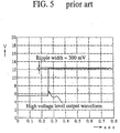
- FIG. 5 is a diagram illustrative of a result of the simulation to the second conventional circuit of FIG. 4.
- the ripple width of the high voltage output is reduced to 300 mV, provided that the speed up capacitance Cl is 0.3 pF.
- the further provision of the speed up capacitor of the second conventional high voltage generating circuit reduces the ripple width or improves the accuracy in voltage level of the high voltage output, however, with the increase in the occupied area of the high voltage generating circuit. In the above circumstances, it had been required to develop a novel high voltage generating circuit free from the above problem.
- the present invention provides a circuitry comprising : a first circuit for rising a voltage level, the first circuit having an output terminal connected to a high voltage output line for outputting a high voltage output ; a comparator having an output terminal connected to an input side of the first circuit, the comparator further having a first input terminal and a second input terminal for receiving a reference voltage ; and a voltage dividing circuit connected between the high voltage output line and a low voltage line having a substantially fixed lower potential than the high voltage output line, the voltage dividing circuit having an output node which is connected to the first input terminal of the comparator for outputting a divided voltage output; and the voltage dividing circuit having at least a resistance between the output node and the high voltage output line, wherein a parasitic capacitance of the at least resistance between the output node and the high voltage output line is connected to the high voltage output line.
- FIG. 1 is a circuit diagram illustrative of a first conventional high voltage generating circuit for generating a highly accurate high voltage for writing and erasing operations of the non-volatile semiconductor memory.
- FIG. 2 shows a ripple width "v" represented by a vertical arrow mark, an expected level represented a horizontal broken line, delay times of the comparator represented by two horizontal short arrow marks and a delay of the voltage-dividing resistance represented by a horizontal long arrow mark.
- FIG. 3 is a diagram illustrative of a result of the simulation to the first conventional circuit of FIG. 1.
- FIG. 4 is a circuit diagram illustrative of a second conventional high voltage generating circuit for generating a highly accurate high voltage for writing and erasing operations of the non-volatile semiconductor memory.
- FIG. 5 is a diagram illustrative of a result of the simulation to the second conventional circuit of FIG. 4.
- FIG. 6 is a circuit diagram illustrative of a first novel high voltage generating circuit for generating a highly accurate high voltage for writing and erasing operations of the non-volatile semiconductor memory in a first embodiment according to the present invention.
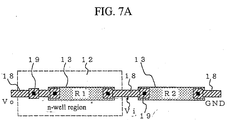
- FIG. 7A is a fragmentary plane view illustrative of the voltage-dividing circuit of the first novel high voltage generating circuit in FIG. 6 realized in the semiconductor integrated circuit in the first embodiment in accordance with the present invention.
- FIG. 7B is a fragmentary cross sectional elevation view illustrative of the voltage-dividing circuit of the first novel high voltage generating circuit in FIG. 6 realized in the semiconductor integrated circuit in the first embodiment in accordance with the present invention.
- FIG. 8 is a diagram illustrative of the waveform of the high voltage output of the first novel high voltage generating circuit of FIG. 6.
- FIG. 9 is a diagram illustrative of a result of the simulation to the first novel circuit of FIG. 6.
- FIG. 10 is a circuit diagram illustrative of a second novel high voltage generating circuit for generating a highly accurate high voltage for writing and erasing operations of the non-volatile semiconductor memory in a second embodiment according to the present invention.
- FIG. 11 is a fragmentary cross sectional elevation view illustrative of the voltage-dividing circuit of the second novel high voltage generating circuit in FIG. 10 realized in the semiconductor integrated circuit in the second embodiment in accordance with the present invention.
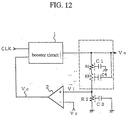
- FIG. 12 is a circuit diagram illustrative of a third novel high voltage generating circuit for generating a highly accurate high voltage for writing and erasing operations of the non-volatile semiconductor memory in a third embodiment according to the present invention.
- the first present invention provides a circuitry comprising : a first circuit for rising a voltage level, the first circuit having an output terminal connected to a high voltage output line for outputting a high voltage output; a comparator having an output terminal connected to an input side of the first circuit, the comparator further having a first input terminal and a second input terminal for receiving a reference voltage ; and a voltage dividing circuit connected between the high voltage output line and a low voltage line having a substantially fixed lower potential than the high voltage output line, the voltage dividing circuit having an output node which is connected to the first input terminal of the comparator for outputting a divided voltage output; and the voltage dividing circuit having at least a resistance between the output node and the high voltage output line, wherein a parasitic capacitance of the at least resistance between the output node and the high voltage output line is connected to the high voltage output line.
- the at least resistance between the output node and the high voltage output line comprises a plurality of resistances connected in series, and a parasitic capacitance of at least closest one of the resistances to the output node is connected to the high voltage output line. It is further preferable that parasitic capacitances of all of the resistances are connected to the high voltage output line. It is further more preferable that the resistances have further parasitic capacitances connected to each other. It is also preferable that the at least resistance between the output node and the high voltage output line comprises two resistances connected in series, and parasitic capacitances of the two resistances are connected to the high voltage output line.
- the at least resistance between the output node and the high voltage output line comprises two resistances connected in series, and a parasitic capacitance of first one of the two resistances closer to the output node is connected to the high voltage output line and a parasitic capacitance of second one of the two resistances closer to the high voltage line is connected to the low voltage line.
- the first circuit comprises a booster circuit.
- the low voltage line comprises a ground line.
- resistances of the voltage dividing circuit comprises electrically conductive layers provided in an insulating layer extending over a semiconductor substrate, and the electrically conductive layer of the at least resistance between the output node and the high voltage output line is positioned over a well region in the semiconductor substrate and is isolated by the insulating layer, so that a parasitic capacitance of the at least resistance is formed between the well region and the electrically conductive layer, and the well region is electrically connected to the high voltage output line.
- the well region has a first conductivity type and the semiconductor substrate has a second conductivity type and the semiconductor substrate is electrically connected to the low voltage line.
- the low voltage line comprises a ground line.
- the high voltage output line, the output node and the low voltage are provided over a top surface of the insulating layer.
- the electrically conductive layers comprise polysilicon layers.
- the at least resistance between the output node and the high voltage output line comprises first and second resistances, and the first resistance comprises a first electrically conductive layer extending over a first insulating layer which extending over a well region in a semiconductor substrate, and the well region is electrically connected to the high voltage output line, and a parasitic capacitance of the first resistance is provided across the first insulating layer between the well region and the first electrically conductive layer; and the second resistance comprises a second electrically conductive layer extending over a second insulating layer which extending over the first electrically conductive layer, and the second electrically conductive layer is electrically connected to the high voltage output line.
- the well region has a first conductivity type and the semiconductor substrate has a second conductivity type and the semiconductor substrate is electrically connected to the low voltage line.
- the low voltage line comprises a ground line.
- the first and second electrically conductive layers comprise polysilicon layers.
- the voltage dividing circuit has at least a low voltage side resistance between the output node and the low voltage line, and a parasitic capacitance of the at least low voltage side resistance is connected to the low voltage line.
- the second present invention provides a high voltage generating circuit in a semiconductor device comprising : a booster circuit having a first input terminal for receiving a clock signal and a second input terminal, and also the booster circuit having an output terminal connected to a high voltage output line for outputting a high voltage output ; a comparator having an output terminal connected to the second input terminal of the booster circuit, the comparator further having a first input terminal and a second input terminal for receiving a reference voltage ; and a voltage dividing circuit connected between the high voltage output line and a low voltage line having a substantially fixed lower potential than the high voltage output line, the voltage dividing circuit having an output node which is connected to the first input terminal of the comparator for outputting a divided voltage output ; and the voltage dividing circuit having at least a resistance between the output node and the high voltage output line, and the voltage dividing circuit having at least a low voltage side resistance between the output node and the low voltage line, wherein a parasitic capacitance of the at least resistance between the output node and the high voltage output
- the at least resistance between the output node and the high voltage output line comprises a plurality of resistances connected in series, and a parasitic capacitance of at least closest one of the resistances to the output node is connected to the high voltage output line. It is further preferable that parasitic capacitances of all of the resistances are connected to the high voltage output line. It is further more preferable that the resistances have further parasitic capacitances connected to each other. It is moreover preferable that the at least resistance between the output node and the high voltage output line comprises two resistances connected in series, and parasitic capacitances of the two resistances are connected to the high voltage output line.
- the at least resistance between the output node and the high voltage output line comprises two resistances connected in series, and a parasitic capacitance of first one of the two resistances closer to the output node is connected to the high voltage output line and a parasitic capacitance of second one of the two resistances closer to the high voltage line is connected to the low voltage line.
- the low voltage line comprises a ground line.
- resistances of the voltage dividing circuit comprises electrically conductive layers provided in an insulating layer extending over a semiconductor substrate, and the electrically conductive layer of the at least resistance between the output node and the high voltage output line is positioned over a well region in the semiconductor substrate and is isolated by the insulating layer, so that a parasitic capacitance of the at least resistance is formed between the well region and the electrically conductive layer, and the well region is electrically connected to the high voltage output line.
- the well region has a first conductivity type and the semiconductor substrate has a second conductivity type and the semiconductor substrate is electrically connected to the low voltage line.
- the low voltage line comprises a ground line.
- the high voltage output line, the output node and the low voltage are provided over a top surface of the insulating layer.
- the electrically conductive layers comprise polysilicon layers.
- the at least resistance between the output node and the high voltage output line comprises first and second resistances, and the first resistance comprises a first electrically conductive layer extending over a first insulating layer which extending over a well region in a semiconductor substrate, and the well region is electrically connected to the high voltage output line, and a parasitic capacitance of the first resistance is provided across the first insulating layer between the well region and the first electrically conductive layer; and the second resistance comprises a second electrically conductive layer extending over a second insulating layer which extending over the first electrically conductive layer, and the second electrically conductive layer is electrically connected to the high voltage output line.
- the well region has a first conductivity type and the semiconductor substrate has a second conductivity type and the semiconductor substrate is electrically connected to the low voltage line. It is still further preferable that the low voltage line comprises a ground line. It is also preferable that the first and second electrically conductive layers comprise polysilicon layers.
- FIG. 6 is a circuit diagram illustrative of a first novel high voltage generating circuit for generating a highly accurate high voltage for writing and erasing operations of the non-volatile semiconductor memory in a first embodiment according to the present invention.
- the first novel high voltage generating circuit comprises a booster circuit 1, a comparator 2, and a voltage dividing circuit which further comprises a series connection of first and second voltage dividing resistances R1 and R2.
- the booster circuit 1 has a first input terminal for receiving a clock signal CLK and a second input terminal connected to an output terminal of the comparator 2 for receiving a control signal Vc from the comparator 2.
- the booster circuit 1 generates a high voltage output Vo which is outputted from its output terminal.
- the voltage dividing circuit which comprises the series connection of the first and second voltage-dividing resistances R1 and R2, is provided between the high voltage output line connected to the output terminal of the booster circuit 1 and a ground line.
- the first voltage-dividing resistance R1 is connected in series between the output terminal of the booster circuit 1 and the second voltage-dividing resistance R2.
- the second voltage-dividing resistance R2 is connected in series between the ground terminal and the first voltage-dividing resistance R1.
- An output node N1 is provided at an intermediate point between the first and second voltage-dividing resistances R1 and R2. Namely, the first voltage-dividing resistance R1 is connected in series between the high voltage output line and the output node N1 of the voltage dividing circuit.
- the second voltage-dividing resistance R2 is connected in series between the ground line and the output node N1 of the voltage dividing circuit.
- the comparator 2 has a first input terminal connected to the output node N1 of the voltage-dividing circuit or the intermediate point between the first and second voltage dividing resistances R1 and R2 for receiving a voltage Vi divided by the voltage-dividing circuit.
- the comparator 2 also has a second input terminal for receiving a reference voltage Vr for allowing the voltage Vi to be compared with the reference voltage Vr, whereby the comparator 2 generates the control signal Vc and output the same from its output terminal.
- the first voltage dividing resistance R1 connected in series between the high voltage output line and the output node N1 of the voltage dividing circuit has a first parasitic capacitance C1.
- the second voltage dividing resistance R2 connected in series between the ground line and the output node N1 of the voltage dividing circuit has a second parasitic capacitance C3.
- the resistance values of the first and second voltage-dividing resistances R1 and R2 are required to be high, provided that the high relative accuracy in resistance value of each of the first and second voltage-dividing resistances R1 and R2 is also necessary.
- the first and second voltage-dividing resistances R1 and R2 may further comprise polysilicon resistances which are low in bias-dependency and are suitable to be higher resistances than the diffusion resistances.
- the first and second voltage-dividing resistances R1 and R2 need larger occupying areas than other resistances, whereby the larger occupying areas of the first and second voltage-dividing resistances R1 and R2 result in the increases in first and second parasitic capacitances C1 and C3.
- the first voltage-dividing resistance R1 has a first time constant which is defined by the resistance value and the parasitic capacitance value thereof.
- the second voltage-dividing resistance R2 has a second time constant which is defined by the resistance value and the parasitic capacitance value thereof. The accuracy in the voltage level of the high voltage output depends on the time constant.
- the first parasitic capacitance C1 is connected to an output terminal of the first novel high voltage generating circuit, wherein the output terminal of the first novel high voltage generating circuit is connected to the output terminal of the booster circuit 1, so that the first parasitic capacitance C1 serves as a speed up capacitor.
- the second parasitic capacitance C3 is connected to the ground line.
- the first parasitic capacitance C1 of the first voltage dividing resistance R1 is connected to an output terminal of the first novel high voltage generating circuit, so that the first parasitic capacitance C1 serves as a speed up capacitor. It is unnecessary to further provide any further speed up capacitor. Accordingly, the first parasitic capacitor serving as the speed up capacitor of the first voltage dividing resistance R1 reduces the ripple width or improves the accuracy in voltage level of the high voltage output without, however, any further increase in the occupied area of the high voltage generating circuit.
- FIG. 7A is a fragmentary plane view illustrative of the voltage-dividing circuit of the first novel high voltage generating circuit in FIG. 6 realized in the semiconductor integrated circuit in the first embodiment in accordance with the present invention.
- FIG. 7B is a fragmentary cross sectional elevation view illustrative of the voltage-dividing circuit of the first novel high voltage generating circuit in FIG. 6 realized in the semiconductor integrated circuit in the first embodiment in accordance with the present invention.
- a p-type semiconductor substrate 10 has an n-well region 11 in it selective upper region.
- An insulating film 12 extends over the p-type semiconductor substrate 10 and the n-well region 11.
- a first polysilicon layer 13-1 is selectively formed in the insulating layer 12 at a predetermined depth, so that the first polysilicon layer 13-1 is positioned over the n-well region 11 and isolated from the n-well region 11 by the insulating layer 12, and also that the first polysilicon layer 13-1 is completely buried in the insulating layer 12 so that the top surface of the first polysilicon layer 13-1 is covered by the insulating layer 12.
- the first parasitic capacitor C1 is formed between the first polysilicon layer 13-1 and the n-well region 11.
- a second polysilicon layer 13-2 is selectively formed in the insulating layer 12 at a predetermined depth, so that the second polysilicon layer 13-2 is positioned at the same depth or the same level as the first polysilicon layer 13-1 and isolated from the first polysilicon layer 13-1 by the insulating layer 12.
- the second polysilicon layer 13-2 is also isolated from the semiconductor substrate 10 by the insulating layer 12, and also that the first polysilicon layer 13-1 is completely buried in the insulating layer 12 so that the top surface of the first polysilicon layer 13-1 is covered by the insulating layer 12.
- the second parasitic capacitor C3 is formed between the second polysilicon layer 13-2 and the semiconductor substrate 10.
- a first interconnection 18-1 is selectively provided on the top surface of the insulating layer 12.
- the first interconnection 18-1 may be made of aluminum.
- the first interconnection 18-1 has a ground potential, so that the first interconnection 18-1 serves as a ground line.
- the first interconnection 18-1 is electrically connected through a first contact 19-1 to the second polysilicon layer 13-2.
- the second polysilicon layer 13-2 serves as the second voltage-dividing resistance R2.
- a second interconnection 18-2 is selectively provided on the top surface of the insulating layer 12.
- the second interconnection 18-2 may be made of aluminum.
- the second interconnection 18-2 has the divided voltage level Vi, so that the second interconnection 18-2 serves as a voltage dividing line connecting the output terminal of the voltage dividing circuit and the first input terminal of the comparator.
- the second interconnection 18-2 is electrically connected through a second contact 19-2 to the second polysilicon layer 13-2.
- the second interconnection 18-2 is also electrically connected through a third contact 19-3 to the first polysilicon layer 13-1.
- the first polysilicon layer 13-1 serves as the first voltage dividing resistance R1.
- a third interconnection 18-3 is selectively provided on the top surface of the insulating layer 12.
- the third interconnection 18-3 may be made of aluminum.
- the third interconnection 18-3 has the high voltage output Vo, so that the third interconnection 18-3 serves as a high voltage output line connected the output terminal of the booster circuit 1.
- the third interconnection 18-3 is electrically connected through a fourth contact 19-4 to the first polysilicon layer 13-1 serving as the first voltage-dividing resistance R1.
- the third interconnection 18-3 serves as a high voltage output line is further connected through a fifth contact 19-5 to the n-well region 11.
- the first parasitic capacitance C1 is formed between the first polysilicon layer 13-1 serving as the first voltage dividing resistance R1 and the n-well region 11 which is further connected through the first contact 19 to the third interconnection 18-3. serves as the high voltage output line.
- the second parasitic capacitance C2 is formed between the second polysilicon layer 13-2 serving as the second voltage dividing resistance R2 and the p-type semiconductor substrate 10 which is grounded.
- FIG. 8 is a diagram illustrative of the waveform of the high voltage output of the first novel high voltage generating circuit of FIG. 6.
- FIG. 8 shows a ripple width "v" represented by a vertical arrow mark, an expected level represented a horizontal broken line, and delay times of the comparator represented by two horizontal short arrow marks.
- the first time constant is defined by the first voltage-dividing resistance R1 and the first parasitic capacitance C2.
- the second time constant is defined by the second voltage-dividing resistance R2 and the second parasitic capacitance C3.
- the high voltage level of the high voltage output line is transmitted through the first parasitic capacitor C1 to the dividing voltage line having the divided voltage Vi appearing on the output terminal between the first and second voltage-dividing resistances R1 and R2 of the voltage-dividing circuit, thereby resulting in a remarkable reduction in a delay time of the feed-back path from the output terminal of the booster circuit 1 to the output terminal of the comparator 2.
- this remarkably reduced delay time period it is difficult to control the booster circuit, whereby the high voltage output has a reduced ripple width and a non-deteriorated accuracy in its voltage level.
- the ripple width is given by the following equation.
- V Dt2 ⁇ Vdt
- Dt2 is the delay of the comparator
- Vdt is a voltage rising rate per a unit time or a boosting capability, provided the delay of the voltage-dividing resistances is approximated zero.
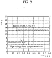
- FIG. 9 is a diagram illustrative of a result of the simulation to the first novel circuit of FIG. 6.
- the ripple width of the high voltage output is 350 mV provided that the first parasitic capacitance C1 of the first voltage dividing resistance is 1 pF.
- the reduced ripple width means the high accuracy in voltage level of the high voltage output.
- the first parasitic capacitance C1 of the first voltage dividing resistance R1 is connected to an output terminal of the first novel high voltage generating circuit, so that the first parasitic capacitance C1 serves as a speed up capacitor. It is unnecessary to further provide any further speed up capacitor. Accordingly, the first parasitic capacitor serving as the speed up capacitor of the first voltage dividing resistance R1 reduces the ripple width or improves the accuracy in voltage level of the high voltage output without, however, any further increase in the occupied area of the high voltage generating circuit.
- FIG. 10 is a circuit diagram illustrative of a second novel high voltage generating circuit for generating a highly accurate high voltage for writing and erasing operations of the non-volatile semiconductor memory in a second embodiment according to the present invention.
- the second novel high voltage generating circuit comprises a booster circuit 1, a comparator 2, and a voltage dividing circuit which further comprises a series connection of first, second and third voltage dividing resistances R1, R2 and R3.
- the booster circuit 1 has a first input terminal for receiving a clock signal CLK and a second input terminal connected to an output terminal of the comparator 2 for receiving a control signal Vc from the comparator 2.
- the booster circuit 1 generates a high voltage output Vo which is outputted from its output terminal.
- the voltage dividing circuit which comprises the series connection of the first, second and third voltage-dividing resistances R1, R2 and R3, is provided between the high voltage output line connected to the output terminal of the booster circuit 1 and a ground line.
- the first and third voltage-dividing resistances R1 and R3 are connected in series between the output terminal of the booster circuit 1 and the second voltage-dividing resistance R2.
- the first voltage-dividing resistance R1 is connected in series between the high voltage output line and the third voltage-dividing resistance R1.
- the third voltage-dividing resistance R3 is connected in series between the first voltage-dividing resistance R1 and the second voltage-dividing resistance R2.
- the second voltage-dividing resistance R2 is connected in series between the ground terminal and the third voltage-dividing resistance R3.
- An output node N1 is provided at an intermediate point between the third and second voltage-dividing resistances R3 and R2.
- the first and third voltage-dividing resistances R1 and R3 are connected in series between the high voltage output line and the output node N1 of the voltage dividing circuit.
- the first voltage-dividing resistance R1 is connected in series between the high voltage output line and the third voltage-dividing resistance R3.
- the third voltage-dividing resistance R3 is connected in series between the first voltage-dividing resistance R1 and the output node N1 of the voltage dividing circuit.
- the second voltage-dividing resistance R2 is connected in series between the ground line and the output node N1 of the voltage dividing circuit.
- the comparator 2 has a first input terminal connected to the output node N1 of the voltage-dividing circuit or the intermediate point between the third and second voltage dividing resistances R3 and R2 for receiving a voltage Vi divided by the voltage-dividing circuit.
- the comparator 2 also has a second input terminal for receiving a reference voltage Vr for allowing the voltage Vi to be compared with the reference voltage Vr, whereby the comparator 2 generates the control signal Vc and output the same from its output terminal.
- the first voltage dividing resistance R1 has a first parasitic capacitance C1 which is connected to the high voltage output line.
- the second voltage dividing resistance R2 has a second parasitic capacitance C3 which is connected to the ground line.
- the third voltage dividing resistance R3 has a third parasitic capacitance C4 which is connected to the high voltage output line. Further, a fourth parasitic capacitance C5 is provided between the first and third voltage dividing resistances R1 and R3.
- the resistance values of the first and second voltage-dividing resistances R1 and R2 are required to be high, provided that the high relative accuracy in resistance value of each of the first and second voltage-dividing resistances R1 and R2 is also necessary.
- the first, second, third and fourth voltage-dividing resistances R1, R2, R3 and R4 may further comprise polysilicon resistances which are low in bias-dependency and are suitable to be higher resistances than the diffusion resistances.
- the first, second and third voltage-dividing resistances R1, R2 and R3 need larger occupying areas than other resistances, whereby the larger occupying areas of the first, second and third voltage-dividing resistances R1, R2 and R3 result in the increases in first, second, third and fourth parasitic capacitances C1, C3, C4 and C5.
- the first voltage-dividing resistance R1 has a first time constant which is defined by the resistance value and the parasitic capacitance value thereof.
- the second voltage-dividing resistance R2 has a second time constant which is defined by the resistance value and the parasitic capacitance value thereof. The accuracy in the voltage level of the high voltage output depends on the time constant.
- the first parasitic capacitance C1 is connected to the high voltage output line connected to the output terminal of the booster circuit 1, so that the first parasitic capacitance C1 serves as a speed up capacitor.
- the second parasitic capacitance C3 is connected to the ground line.
- the third parasitic capacitance C4 is also connected to the high voltage output line connected to the output terminal of the booster circuit 1, so that the third parasitic capacitance C4 serves as a speed up capacitor.
- the first parasitic capacitance C1 of the first voltage dividing resistance R1 is connected to the high voltage output line, so that the first parasitic capacitance C1 serves as a speed up capacitor, and further the third parasitic capacitance C4 of the third voltage dividing resistance R3 is also connected to the high voltage output line, so that the first and third parasitic capacitances C1 and C4 serve as a speed up capacitor. It is unnecessary to further provide any further speed up capacitor. Accordingly, the first parasitic capacitor C1 and the third parasitic capacitor C4 serving as the speed up capacitor reduces the ripple width or improves the accuracy in voltage level of the high voltage output without, however, any further increase in the occupied area of the high voltage generating circuit.
- FIG. 11 is a fragmentary cross sectional elevation view illustrative of the voltage-dividing circuit of the second novel high voltage generating circuit in FIG. 10 realized in the semiconductor integrated circuit in the second embodiment in accordance with the present invention.
- An n-well region 11 is selectively provided in a p-type semiconductor substrate 10.
- the n-well region 11 is connected through a non-illustrated contact to the high voltage output line not illustrated.
- a first insulating layer 12 is provided which extends over a top surface of the n-well region 11 and the top surface of the p-type semiconductor substrate 10.
- a first polysilicon layer 13 serving as the first voltage-dividing resistance R1 is selectively provided which extends over the top surface of the first insulating layer 12.
- the first polysilicon layer 13 is positioned indirectly over the n-well region 11, which is connected to the high voltage output line, whereby the first parasitic capacitance 14 as the capacitance C1 is formed across the first insulting layer 12 between the well region 11 and the first polysilicon layer 13 serving as the first voltage-dividing resistance R1.
- a second insulting layer 15 is provided which extends over the top surface of the first polysilicon layer 13.
- a second polysilicon layer 16 serving as the third voltage-dividing resistance R3 is selectively provided which extends over the top surface of the second insulating layer 15.
- a fifth parasitic capacitance 17 of the capacitance value C5 is formed across the second insulating layer 15 between the first polysilicon layer 13 and the second polysilicon layer 16.
- the second polysilicon layer 16 is connected to the output node N1 of the voltage dividing circuit.
- the second polysilicon layer 16 is further isolated by an insulation layer not illustrated from the high voltage output line, so that the third parasitic capacitance C4 is formed across the insulation layer not illustrated.
- the first and second polysilicon layers 13 and 16 are included in the lamination structure, so that no increase in occupied area of the circuit is cased even the two speed up capacitors are provided to further reduce the ripple width.
- the high voltage output line are connected to all of the parasitic capacitances processed by all of the voltage dividing resistances connected in series between the high voltage output line and the output node N1 of the voltage dividing circuit. Accordingly, the first parasitic capacitor C1 and the third parasitic capacitor C4 serving as the speed up capacitor further reduces the ripple width or improves the accuracy in voltage level of the high voltage output without, however, any further increase in the occupied area of the high voltage generating circuit.
- FIG. 12 is a circuit diagram illustrative of a third novel high voltage generating circuit for generating a highly accurate high voltage for writing and erasing operations of the non-volatile semiconductor memory in a third embodiment according to the present invention.
- the third novel high voltage generating circuit comprises a booster circuit 1, a comparator 2, and a voltage dividing circuit which further comprises a series connection of first, second and third voltage dividing resistances R1, R2 and R3.
- the booster circuit 1 has a first input terminal for receiving a clock signal CLK and a second input terminal connected to an output terminal of the comparator 2 for receiving a control signal Vc from the comparator 2.
- the booster circuit 1 generates a high voltage output Vo which is outputted from its output terminal.
- the voltage dividing circuit which comprises the series connection of the first, second and third voltage-dividing resistances R1, R2 and R3, is provided between the high voltage output line connected to the output terminal of the booster circuit 1 and a ground line.
- the first and third voltage-dividing resistances R1 and R3 are connected in series between the output terminal of the booster circuit 1 and the second voltage-dividing resistance R2.
- the first voltage-dividing resistance R1 is connected in series between the high voltage output line and the third voltage-dividing resistance R1.
- the third voltage-dividing resistance R3 is connected in series between the first voltage-dividing resistance R1 and the second voltage-dividing resistance R2.
- the second voltage-dividing resistance R2 is connected in series between the ground terminal and the third voltage-dividing resistance R3.
- An output node N1 is provided at an intermediate point between the third and second voltage-dividing resistances R3 and R2.
- the first and third voltage-dividing resistances R1 and R3 are connected in series between the high voltage output line and the output node N1 of the voltage dividing circuit.
- the first voltage-dividing resistance R1 is connected in series between the high voltage output line and the third voltage-dividing resistance R3.
- the third voltage-dividing resistance R3 is connected in series between the first voltage-dividing resistance R1 and the output node N1 of the voltage dividing circuit.
- the second voltage-dividing resistance R2 is connected in series between the ground line and the output node N1 of the voltage dividing circuit.
- the comparator 2 has a first input terminal connected to the output node N1 of the voltage-dividing circuit or the intermediate point between the third and second voltage dividing resistances R3 and R2 for receiving a voltage Vi divided by the voltage-dividing circuit.
- the comparator 2 also has a second input terminal for receiving a reference voltage Vr for allowing the voltage Vi to be compared with the reference voltage Vr, whereby the comparator 2 generates the control signal Vc and output the same from its output terminal.
- the first voltage dividing resistance R1 has a first parasitic capacitance C1 which is connected to the ground line.
- the second voltage dividing resistance R2 has a second parasitic capacitance C3 which is also connected to the ground line.
- the third voltage dividing resistance R3 has a third parasitic capacitance C4 which is connected to the high voltage output line.
- the resistance values of the first and second voltage-dividing resistances R1 and R2 are required to be high, provided that the high relative accuracy in resistance value of each of the first and second voltage-dividing resistances R1 and R2 is also necessary.
- the first, second, third and fourth voltage-dividing resistances R1, R2, R3 and R4 may further comprise polysilicon resistances which are low in bias-dependency and are suitable to be higher resistances than the diffusion resistances.
- the first, second and third voltage-dividing resistances R1, R2 and R3 need larger occupying areas than other resistances, whereby the larger occupying areas of the first, second and third voltage-dividing resistances R1, R2 and R3 result in the increases in first, second and third parasitic capacitances C1, C3 and C4.
- the first voltage-dividing resistance R1 has a first time constant which is defined by the resistance value and the parasitic capacitance value thereof.
- the second voltage-dividing resistance R2 has a second time constant which is defined by the resistance value and the parasitic capacitance value thereof. The accuracy in the voltage level of the high voltage output depends on the time constant.
- the first parasitic capacitance C1 is connected to the ground line.
- the second parasitic capacitance C3 is also connected to the ground line.
- the third parasitic capacitance C4 is also connected to the high voltage output line connected to the output terminal of the booster circuit 1, so that the third parasitic capacitance C4 serves as a speed up capacitor.
- the third parasitic capacitance C4 of the third voltage dividing resistance R3, which is closer to the output node N1 of the voltage dividing circuit is connected to the high voltage output line, so that the third parasitic capacitance C4 serves as a speed up capacitor. It is unnecessary to further provide any further speed up capacitor. Accordingly, the third parasitic capacitor C4 serving as the speed up capacitor reduces the ripple width or improves the accuracy in voltage level of the high voltage output without, however, any further increase in the occupied area of the high voltage generating circuit.
- the high voltage output line is connected to the parasitic capacitance C4 of the voltage dividing resistance R3 which is closer to the output node N1 of the voltage dividing circuit and which is positioned in the higher voltage side than the output node N1, then the effect of reducing the ripple width is greater as compared to the other case wherein the high voltage output line is connected to the parasitic capacitance C1 of the voltage dividing resistance R1 which is closer to the high voltage output line. Notwithstanding, it is most preferable that the high voltage output line is connected to both the parasitic capacitances c1 and C4 of the voltage dividing resistances R1 and R3 as in the second embodiment.
Landscapes
- Engineering & Computer Science (AREA)
- Power Engineering (AREA)
- Physics & Mathematics (AREA)
- Condensed Matter Physics & Semiconductors (AREA)
- General Physics & Mathematics (AREA)
- Computer Hardware Design (AREA)
- Microelectronics & Electronic Packaging (AREA)
- Semiconductor Integrated Circuits (AREA)
- Read Only Memory (AREA)
- Manipulation Of Pulses (AREA)
Applications Claiming Priority (2)
| Application Number | Priority Date | Filing Date | Title |
|---|---|---|---|
| JP2000049126A JP3372923B2 (ja) | 2000-02-25 | 2000-02-25 | 半導体集積回路 |
| JP2000049126 | 2000-02-25 |
Publications (2)
| Publication Number | Publication Date |
|---|---|
| EP1128534A2 true EP1128534A2 (fr) | 2001-08-29 |
| EP1128534A3 EP1128534A3 (fr) | 2003-09-24 |
Family
ID=18571109
Family Applications (1)
| Application Number | Title | Priority Date | Filing Date |
|---|---|---|---|
| EP01103595A Withdrawn EP1128534A3 (fr) | 2000-02-25 | 2001-02-21 | Circuit générateur de haute tension avec capacitance parasite améliorée de la résistance divisant la tension |
Country Status (5)
| Country | Link |
|---|---|
| US (1) | US6531912B2 (fr) |
| EP (1) | EP1128534A3 (fr) |
| JP (1) | JP3372923B2 (fr) |
| KR (1) | KR100426401B1 (fr) |
| TW (1) | TW529157B (fr) |
Cited By (2)
| Publication number | Priority date | Publication date | Assignee | Title |
|---|---|---|---|---|
| CN104811075A (zh) * | 2014-12-12 | 2015-07-29 | 武汉绿鼎天舒科技发展有限公司 | 一种组合变换器的控制方法 |
| CN104821784A (zh) * | 2014-12-12 | 2015-08-05 | 武汉绿鼎天舒科技发展有限公司 | 一种使用升压电路的太阳能电池 |
Families Citing this family (24)
| Publication number | Priority date | Publication date | Assignee | Title |
|---|---|---|---|---|
| DE10108980A1 (de) * | 2001-02-23 | 2002-09-12 | Koninkl Philips Electronics Nv | Anordnung zur Ansteuerung von Anzeigeeinheiten mit adaptiver Startsequenz |
| JP4803898B2 (ja) * | 2001-05-17 | 2011-10-26 | ルネサスエレクトロニクス株式会社 | 半導体装置 |
| US7941675B2 (en) | 2002-12-31 | 2011-05-10 | Burr James B | Adaptive power control |
| US7112978B1 (en) | 2002-04-16 | 2006-09-26 | Transmeta Corporation | Frequency specific closed loop feedback control of integrated circuits |
| US7953990B2 (en) | 2002-12-31 | 2011-05-31 | Stewart Thomas E | Adaptive power control based on post package characterization of integrated circuits |
| US7228242B2 (en) | 2002-12-31 | 2007-06-05 | Transmeta Corporation | Adaptive power control based on pre package characterization of integrated circuits |
| US7454393B2 (en) * | 2003-08-06 | 2008-11-18 | Microsoft Corporation | Cost-benefit approach to automatically composing answers to questions by extracting information from large unstructured corpora |
| KR100526344B1 (ko) | 2003-08-12 | 2005-11-08 | 삼성전자주식회사 | 승압 전압 제어장치 및 방법 |
| US6859091B1 (en) * | 2003-09-18 | 2005-02-22 | Maxim Integrated Products, Inc. | Continuous linear regulated zero dropout charge pump with high efficiency load predictive clocking scheme |
| KR100564575B1 (ko) * | 2003-09-23 | 2006-03-29 | 삼성전자주식회사 | 부하제어 부스팅 장치, 부하량에 따라 자동적으로부스팅을 결정하고 커패시터 수가 적은 부스팅 파워시스템 및 그 방법 |
| TW200526588A (en) * | 2003-11-17 | 2005-08-16 | Smithkline Beecham Corp | Chemical compounds |
| KR100462520B1 (ko) * | 2003-11-27 | 2004-12-17 | 주식회사 포인칩스 | 고전압 구동신호를 발생시키는 액체렌즈 구동회로 |
| US7649402B1 (en) | 2003-12-23 | 2010-01-19 | Tien-Min Chen | Feedback-controlled body-bias voltage source |
| US7012461B1 (en) | 2003-12-23 | 2006-03-14 | Transmeta Corporation | Stabilization component for a substrate potential regulation circuit |
| US7129771B1 (en) * | 2003-12-23 | 2006-10-31 | Transmeta Corporation | Servo loop for well bias voltage source |
| US7692477B1 (en) | 2003-12-23 | 2010-04-06 | Tien-Min Chen | Precise control component for a substrate potential regulation circuit |
| US7774625B1 (en) | 2004-06-22 | 2010-08-10 | Eric Chien-Li Sheng | Adaptive voltage control by accessing information stored within and specific to a microprocessor |
| US7562233B1 (en) | 2004-06-22 | 2009-07-14 | Transmeta Corporation | Adaptive control of operating and body bias voltages |
| JP5315604B2 (ja) | 2006-09-29 | 2013-10-16 | 富士通セミコンダクター株式会社 | 半導体集積回路 |
| JP2009118605A (ja) * | 2007-11-05 | 2009-05-28 | Toshiba Corp | 電圧発生回路 |
| US8830776B1 (en) * | 2013-03-15 | 2014-09-09 | Freescale Semiconductor, Inc. | Negative charge pump regulation |
| JP5723998B2 (ja) * | 2014-01-15 | 2015-05-27 | ルネサスエレクトロニクス株式会社 | 半導体装置 |
| JP5940691B1 (ja) | 2015-02-04 | 2016-06-29 | ウィンボンド エレクトロニクス コーポレーション | 電圧生成回路、半導体装置およびフラッシュメモリ |
| US10416242B2 (en) * | 2017-09-08 | 2019-09-17 | Invensense, Inc. | High voltage circuitry with drift mitigation |
Citations (3)
| Publication number | Priority date | Publication date | Assignee | Title |
|---|---|---|---|---|
| EP0772283A1 (fr) * | 1995-10-31 | 1997-05-07 | STMicroelectronics S.r.l. | Multiplicateur de tension avec régulation lineaire |
| US5744385A (en) * | 1997-03-21 | 1998-04-28 | Plato Labs, Inc. | Compensation technique for parasitic capacitance |
| EP0862260A2 (fr) * | 1997-02-28 | 1998-09-02 | Seiko Instruments Inc. | Circuit pompe de charge |
Family Cites Families (16)
| Publication number | Priority date | Publication date | Assignee | Title |
|---|---|---|---|---|
| JPS5866351A (ja) | 1981-10-15 | 1983-04-20 | Toshiba Corp | 半導体集積回路装置 |
| JPS59218766A (ja) | 1983-05-27 | 1984-12-10 | Toshiba Corp | 電圧昇圧回路 |
| JPH02241355A (ja) * | 1989-03-13 | 1990-09-26 | Toshiba Corp | 昇圧回路 |
| JP2614938B2 (ja) * | 1990-10-25 | 1997-05-28 | 日本電気アイシーマイコンシステム株式会社 | チャージポンプ装置 |
| US5329168A (en) * | 1991-12-27 | 1994-07-12 | Nec Corporation | Semiconductor integrated circuit device equipped with substrate biasing system selectively powered from internal and external power sources |
| EP0577906B1 (fr) * | 1992-06-30 | 1998-09-23 | STMicroelectronics S.r.l. | Structure évitant la mise à l'état "passant" d'une diode parasite dans une région épitaxiale de circuits intégrés |
| KR0124049B1 (ko) * | 1994-06-30 | 1997-11-25 | 김광호 | 반도체 집적장치의 가변승압회로 |
| JP3638641B2 (ja) * | 1994-10-05 | 2005-04-13 | 株式会社ルネサステクノロジ | 昇圧電位発生回路 |
| JPH08306870A (ja) | 1995-04-28 | 1996-11-22 | Fuji Xerox Co Ltd | 半導体集積昇圧回路装置 |
| JPH10190466A (ja) * | 1996-12-27 | 1998-07-21 | Sony Corp | 半導体集積回路 |
| JPH10201226A (ja) * | 1996-12-30 | 1998-07-31 | Murata Mfg Co Ltd | 高電圧発生回路 |
| JPH1166855A (ja) * | 1997-06-10 | 1999-03-09 | Fujitsu Ltd | 電位検出回路、半導体装置、及び半導体記憶装置 |
| KR19990005631A (ko) * | 1997-06-30 | 1999-01-25 | 윤종용 | 고압전원장치의 제어회로 |
| JP4080043B2 (ja) | 1997-12-24 | 2008-04-23 | 株式会社ルネサステクノロジ | 昇圧回路、半導体記憶装置、及びデータ処理装置 |
| FI107657B (fi) * | 1998-03-11 | 2001-09-14 | Nokia Mobile Phones Ltd | Kytkentä differentiaalisen aktiivikomponentin impedanssin säätämiseksi |
| DE19950543C1 (de) * | 1999-10-20 | 2000-11-23 | Infineon Technologies Ag | Integrierte Schaltung mit Regelung der Einsatzspannungen ihrer Transistoren |
-
2000
- 2000-02-25 JP JP2000049126A patent/JP3372923B2/ja not_active Expired - Fee Related
-
2001
- 2001-02-21 EP EP01103595A patent/EP1128534A3/fr not_active Withdrawn
- 2001-02-23 TW TW090104296A patent/TW529157B/zh not_active IP Right Cessation
- 2001-02-23 US US09/790,491 patent/US6531912B2/en not_active Expired - Fee Related
- 2001-02-24 KR KR10-2001-0009519A patent/KR100426401B1/ko not_active IP Right Cessation
Patent Citations (3)
| Publication number | Priority date | Publication date | Assignee | Title |
|---|---|---|---|---|
| EP0772283A1 (fr) * | 1995-10-31 | 1997-05-07 | STMicroelectronics S.r.l. | Multiplicateur de tension avec régulation lineaire |
| EP0862260A2 (fr) * | 1997-02-28 | 1998-09-02 | Seiko Instruments Inc. | Circuit pompe de charge |
| US5744385A (en) * | 1997-03-21 | 1998-04-28 | Plato Labs, Inc. | Compensation technique for parasitic capacitance |
Cited By (2)
| Publication number | Priority date | Publication date | Assignee | Title |
|---|---|---|---|---|
| CN104811075A (zh) * | 2014-12-12 | 2015-07-29 | 武汉绿鼎天舒科技发展有限公司 | 一种组合变换器的控制方法 |
| CN104821784A (zh) * | 2014-12-12 | 2015-08-05 | 武汉绿鼎天舒科技发展有限公司 | 一种使用升压电路的太阳能电池 |
Also Published As
| Publication number | Publication date |
|---|---|
| JP3372923B2 (ja) | 2003-02-04 |
| KR20010085577A (ko) | 2001-09-07 |
| JP2001237374A (ja) | 2001-08-31 |
| TW529157B (en) | 2003-04-21 |
| KR100426401B1 (ko) | 2004-04-08 |
| US6531912B2 (en) | 2003-03-11 |
| EP1128534A3 (fr) | 2003-09-24 |
| US20010030364A1 (en) | 2001-10-18 |
Similar Documents
| Publication | Publication Date | Title |
|---|---|---|
| EP1128534A2 (fr) | Circuit générateur de haute tension avec capacitance parasite améliorée de la résistance divisant la tension | |
| JP2718375B2 (ja) | チャージポンプ回路 | |
| EP0292269B1 (fr) | Système générateur de haute tension intégré | |
| KR940003891B1 (ko) | 오동작 방지수단을 갖는 반도체장치 | |
| GB2087183A (en) | Semiconductor integrated circuit device | |
| IE52689B1 (en) | Semiconductor memory device | |
| KR950001430B1 (ko) | 전류 감지 증폭 회로 | |
| EP0163384B1 (fr) | Disposition des lignes d'alimentation en puissance dans un circuit intégré | |
| US20060087347A1 (en) | Input circuit and semiconductor device | |
| KR100211481B1 (ko) | 전압 발생 회로가 구비된 반도체 메모리 디바이스 | |
| US4090259A (en) | Means for controlling the gate potential of MNOS transistors in a memory | |
| JPH08107184A (ja) | 昇圧電位発生回路 | |
| US4651306A (en) | Dynamic memory | |
| JP3698550B2 (ja) | ブースト回路及びこれを用いた半導体装置 | |
| KR19980081691A (ko) | 칩면적 및 소비 전력을 감소시킬 수 있는 반도체 집적회로 장치 | |
| EP0248608A1 (fr) | Circuits servant de tampon de sortie | |
| US5615242A (en) | Charge transfer apparatus with output gate and driving method thereof | |
| US7642844B2 (en) | Semiconductor integrated circuit for voltage detection | |
| US4839710A (en) | CMOS cell which can be used as a resistor, a capacitor, an RC component or a terminating impedance of a signal | |
| US4082963A (en) | Regenerating amplifier for ccd arrangements | |
| JPH07298607A (ja) | 半導体昇圧回路 | |
| JP4773746B2 (ja) | 昇圧回路 | |
| KR100299806B1 (ko) | 고속 또한 안정하게 신호를 전달할 수 있는 반도체 장치 | |
| JP2000150789A (ja) | 半導体集積回路 | |
| KR200273612Y1 (ko) | 노이즈에 강한 기판 바이어스전위 감지 장치 |
Legal Events
| Date | Code | Title | Description |
|---|---|---|---|
| PUAI | Public reference made under article 153(3) epc to a published international application that has entered the european phase |
Free format text: ORIGINAL CODE: 0009012 |
|
| AK | Designated contracting states |
Kind code of ref document: A2 Designated state(s): AT BE CH CY DE DK ES FI FR GB GR IE IT LI LU MC NL PT SE TR |
|
| AX | Request for extension of the european patent |
Free format text: AL;LT;LV;MK;RO;SI |
|
| RAP1 | Party data changed (applicant data changed or rights of an application transferred) |
Owner name: NEC ELECTRONICS CORPORATION |
|
| PUAL | Search report despatched |
Free format text: ORIGINAL CODE: 0009013 |
|
| AK | Designated contracting states |
Kind code of ref document: A3 Designated state(s): AT BE CH CY DE DK ES FI FR GB GR IE IT LI LU MC NL PT SE TR |
|
| AX | Request for extension of the european patent |
Extension state: AL LT LV MK RO SI |
|
| 17P | Request for examination filed |
Effective date: 20030818 |
|
| 17Q | First examination report despatched |
Effective date: 20040227 |
|
| AKX | Designation fees paid |
Designated state(s): DE FR IT |
|
| GRAP | Despatch of communication of intention to grant a patent |
Free format text: ORIGINAL CODE: EPIDOSNIGR1 |
|
| STAA | Information on the status of an ep patent application or granted ep patent |
Free format text: STATUS: THE APPLICATION IS DEEMED TO BE WITHDRAWN |
|
| 18D | Application deemed to be withdrawn |
Effective date: 20050627 |