EP1111397A2 - Anordnung zum Testen von Chips mittels einer gedruckten Schaltungsplatte - Google Patents
Anordnung zum Testen von Chips mittels einer gedruckten Schaltungsplatte Download PDFInfo
- Publication number
- EP1111397A2 EP1111397A2 EP00126789A EP00126789A EP1111397A2 EP 1111397 A2 EP1111397 A2 EP 1111397A2 EP 00126789 A EP00126789 A EP 00126789A EP 00126789 A EP00126789 A EP 00126789A EP 1111397 A2 EP1111397 A2 EP 1111397A2
- Authority
- EP
- European Patent Office
- Prior art keywords
- pcb
- chips
- needles
- chip
- testing
- Prior art date
- Legal status (The legal status is an assumption and is not a legal conclusion. Google has not performed a legal analysis and makes no representation as to the accuracy of the status listed.)
- Granted
Links
Images
Classifications
-
- G—PHYSICS
- G01—MEASURING; TESTING
- G01R—MEASURING ELECTRIC VARIABLES; MEASURING MAGNETIC VARIABLES
- G01R1/00—Details of instruments or arrangements of the types included in groups G01R5/00 - G01R13/00 and G01R31/00
- G01R1/02—General constructional details
- G01R1/04—Housings; Supporting members; Arrangements of terminals
- G01R1/0408—Test fixtures or contact fields; Connectors or connecting adaptors; Test clips; Test sockets
- G01R1/0433—Sockets for IC's or transistors
- G01R1/0441—Details
- G01R1/0466—Details concerning contact pieces or mechanical details, e.g. hinges or cams; Shielding
-
- H—ELECTRICITY
- H10—SEMICONDUCTOR DEVICES; ELECTRIC SOLID-STATE DEVICES NOT OTHERWISE PROVIDED FOR
- H10W—GENERIC PACKAGES, INTERCONNECTIONS, CONNECTORS OR OTHER CONSTRUCTIONAL DETAILS OF DEVICES COVERED BY CLASS H10
- H10W72/00—Interconnections or connectors in packages
- H10W72/071—Connecting or disconnecting
- H10W72/072—Connecting or disconnecting of bump connectors
- H10W72/07251—Connecting or disconnecting of bump connectors characterised by changes in properties of the bump connectors during connecting
-
- H—ELECTRICITY
- H10—SEMICONDUCTOR DEVICES; ELECTRIC SOLID-STATE DEVICES NOT OTHERWISE PROVIDED FOR
- H10W—GENERIC PACKAGES, INTERCONNECTIONS, CONNECTORS OR OTHER CONSTRUCTIONAL DETAILS OF DEVICES COVERED BY CLASS H10
- H10W72/00—Interconnections or connectors in packages
- H10W72/20—Bump connectors, e.g. solder bumps or copper pillars; Dummy bumps; Thermal bumps
Definitions
- PCB printed circuit Board
- the testing of chips is preferably carried out at the wafer level, because a large number of chips are processed in parallel can what a significant time and cost saving with brings itself. Lately have become particularly parallel Contacting methods based on needles with small dimensions based on a form factor, for example, regarded as promising. Such tests can basically carried out using two different methods become:
- the first method uses a number of very accurate probe needles provided on each chip, and these sample needles are in contact with pads or contact pads on a PCB brought.
- the probe needles are in large numbers attached to a probe or sample card, which for parallel testing of multiple chips is used.
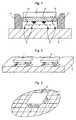
- FIG. 2 The first and second methods are shown in FIG. 2 and FIG 3 illustrates:
- chips 1, 2 are each provided with probe needles 3, brought into contact with pads 4 on a PCB 5 become.
- the second method uses a sample card 6 that is equipped with a large number of such probe needles 3, which in contact with a plurality of chips 1 on one Semiconductor wafers 7 are made of silicon.
- the first method allows the individual to be tested in parallel Chips 1, 2 on the PCB 5, care must be taken that the probe needles 3 each hit their assigned pads 4 and contact them reliably.
- a disadvantage here is that the centering of the individual sample needles on the Pads are difficult to adhere to and that the probe needles continue must be firmly connected to the individual chips, which makes further processing difficult: the test needles can namely practically not removed, so that they the further use of the chips must be taken into account. It’s also a significant expense a complete set of probe needles for each chip realize.
- the second method with the sample card 6 shows the last one mentioned disadvantage of a high expenditure for test needles for not every chip: here the sample card with their Probe needles successively different sets of chips or contact their pads. But it has the disadvantage that a Contacting the chips of an entire semiconductor wafer practically is excluded, because according to the current state of the art the realization of sample cards with some 10,000 individual Trial needles are not possible. But this would be necessary because a semiconductor wafer can have up to 1000 chips can and about 60 sample needles for each of these individual chips are needed, so that a total of the sample card for Testing a wafer or the chips implemented in the wafer 60,000 test needles would be necessary.
- the test needles are not more on the chip, like the first method above, and also no longer on the sample card, as with the above the second method. Rather, the sample needles directly attached to the PCB, so that neither a sample card with the largest possible number of sample needles still sample needles on the individual semiconductor chips are needed.
- the direct attachment of the probe needles to the PCB enables the parallel contacting and testing of a large number of individual chips.
- For testing memory chips in advantageously uses a DIMM-like PCB, because a such PCB testing the memory chip under application conditions allowed.
- interposer can be made of plastic or Plastic and metal exist and is solid with the actual one Chip connected.
- a major advantage of the invention is that in contrast to the prior art according to the above first method the probe needles no longer with the individual Chips are connected. This makes one essential less amount of needles needed because of those on the PCB attached needles for testing the following chips easily can be used.
- the above second usual method must be in the arrangement according to the invention not as exacting requirements as with Sample cards can be made: Through the dummy needles namely a self-centering can be achieved in which by these dummy needles correct adjustment of the sample needles is guaranteed on the pads of the chip or interposer.
- the arrangement according to the invention also allows testing under conditions similar to an actual application the chips. This makes it possible to at safety margins Avoid tests because defective chips are reliably screened out can be.
- a chip is provided with an interposer 8 which in the usual way consists of plastic, in which metal sheets run.
- This interposer 2 can, however, if necessary also be omitted.
- the centering then takes place so that in the uppermost chip layers made of, for example, polyimide and / or silicon dioxide corresponding centering structures be etched.
- FIG. 1 also shows a PCB 5 which, for example, consists of Epoxy resin exists and on the conductor tracks in the usual way run. On these (not shown) conductor tracks or on the surface of the PCB 5 are 9 probe needles at attachment points 3 attached.
- the two in Fig. 1 act entirely outer sample needles that are in recesses 10 of the interposer 8 engage as dummy needles that are not electrically connected for example directly on the surface of the PCB are attached.
- Corresponding leads from these contact pads 12 Conductor tracks through the interposer 8 to the chip 1, see above that its functions can be tested as soon as the probe needles 3 touch the contact pads 12 and thus one Establish electrical connection to a tester, not shown.
- Arrangements as shown in FIG. 1 can be made on the PCB 5 are to be provided side by side in large numbers, so that it is possible to have a large number of chips in parallel at the same time to test on this PCB.
- a tester may be sufficient if the results of the chips lying parallel to one another in a corresponding manner Way to evaluate.
Landscapes
- Physics & Mathematics (AREA)
- General Physics & Mathematics (AREA)
- Engineering & Computer Science (AREA)
- Computer Hardware Design (AREA)
- Microelectronics & Electronic Packaging (AREA)
- Testing Or Measuring Of Semiconductors Or The Like (AREA)
- Measuring Leads Or Probes (AREA)
- Testing Of Individual Semiconductor Devices (AREA)
- Tests Of Electronic Circuits (AREA)
Abstract
Description
- Fig. 1
- eine erfindungsgemäße Anordnung in einer schematischen Schnittdarstellung,
- Fig. 2
- eine herkömmliche Anordnung, die die erste Methode verwendet, bei welcher Probe-Nadeln an einzelnen Chips angebracht sind, und
- Fig. 3
- eine andere herkömmliche Anordnung, bei welcher Probe-Nadeln an einer Probe-Karte angebracht sind.
Claims (5)
- Anordnung zum Testen von Chips (1) mittels einer gedruckten Schaltungsplatte (PCB) (5), bei der eine elektrische Verbindung zwischen der PCB (5) und dem Chip (1) herstellbar ist und auf der PCB (5) mehrere Chips parallel zu testen sind,
dadurch gekennzeichnet, daß die elektrische Verbindung durch direkt auf der PCB (5) angebrachte Probe-Nadeln (3) herstellbar ist und daß auf der PCB (5) zusätzlich als Dummy-Nadeln (3) wirkende Probe-Nadeln zur mechanischen Selbstjustierung der Chips (1) angebracht sind. - Anordnung nach Anspruch 1,
dadurch gekennzeichnet, daß die Dummy-Nadeln (3) mit ihrem von der PCB (5) abgewandten freien Enden in Markierungen eingreifen. - Anordnung nach Anspruch 2,
dadurch gekennzeichnet, daß die Markierungen Vertiefungen (10) sind. - Anordnung nach einem der Ansprüche 1 bis 3,
dadurch gekennzeichnet, daß zwischen den Nadeln (3) und dem Chip (1) ein Zwischenstück (8) vorgesehen ist oder geeignete Strukturen direkt in die Oberfläche des Chips (1) eingebracht sind. - Anordnung nach einem der Ansprüche 1 bis 4,
dadurch gekennzeichnet, daß die PCB (5) mit Justierhilfen (11) zum Ausrichten der Chips (1) versehen ist.
Applications Claiming Priority (2)
| Application Number | Priority Date | Filing Date | Title |
|---|---|---|---|
| DE19961791 | 1999-12-21 | ||
| DE19961791A DE19961791C2 (de) | 1999-12-21 | 1999-12-21 | Anordnung zum Testen von Chips mittels einer gedruckten Schaltungsplatte |
Publications (3)
| Publication Number | Publication Date |
|---|---|
| EP1111397A2 true EP1111397A2 (de) | 2001-06-27 |
| EP1111397A3 EP1111397A3 (de) | 2003-06-25 |
| EP1111397B1 EP1111397B1 (de) | 2005-10-26 |
Family
ID=7933661
Family Applications (1)
| Application Number | Title | Priority Date | Filing Date |
|---|---|---|---|
| EP00126789A Expired - Lifetime EP1111397B1 (de) | 1999-12-21 | 2000-12-06 | Anordnung zum Testen von Chips mittels einer gedruckten Schaltungsplatte |
Country Status (7)
| Country | Link |
|---|---|
| US (1) | US6472892B2 (de) |
| EP (1) | EP1111397B1 (de) |
| JP (1) | JP2001215256A (de) |
| KR (1) | KR100720788B1 (de) |
| CN (1) | CN1294422C (de) |
| DE (2) | DE19961791C2 (de) |
| TW (1) | TW574507B (de) |
Families Citing this family (15)
| Publication number | Priority date | Publication date | Assignee | Title |
|---|---|---|---|---|
| US6682955B2 (en) * | 2002-05-08 | 2004-01-27 | Micron Technology, Inc. | Stacked die module and techniques for forming a stacked die module |
| US7061126B2 (en) * | 2003-10-07 | 2006-06-13 | Hewlett-Packard Development Company, L.P. | Circuit board assembly |
| JP4525117B2 (ja) * | 2004-03-12 | 2010-08-18 | ルネサスエレクトロニクス株式会社 | トレイ |
| US20070024312A1 (en) * | 2005-07-27 | 2007-02-01 | Atmel Germany Gmbh | Device and method for the testing of integrated semiconductor circuits on wafers |
| US8436636B2 (en) | 2006-10-10 | 2013-05-07 | Apple Inc. | Methods and apparatuses for testing circuit boards |
| US8362793B2 (en) | 2006-11-07 | 2013-01-29 | Apple Inc. | Circuit boards including removable test point portions and configurable testing platforms |
| CN101231322B (zh) * | 2007-02-09 | 2011-01-26 | 段超毅 | 集成电路开路/短路的测试连接方法 |
| DE102007015283A1 (de) * | 2007-03-29 | 2008-10-02 | Qimonda Ag | Testvorrichtung für Halbleiterbauelemente |
| CN101770967A (zh) * | 2009-01-03 | 2010-07-07 | 上海芯豪微电子有限公司 | 一种共用基底集成电路测试方法、装置和系统 |
| US8994393B2 (en) | 2012-09-06 | 2015-03-31 | International Business Machines Corporation | High-frequency cobra probe |
| CN103399176B (zh) * | 2013-07-23 | 2015-07-01 | 苏州固锝电子股份有限公司 | 用于加速度传感器的测试系统 |
| CN105575836B (zh) * | 2014-10-08 | 2018-06-12 | 慧荣科技股份有限公司 | 测试装置 |
| CN105895542A (zh) * | 2016-04-20 | 2016-08-24 | 上海斐讯数据通信技术有限公司 | 芯片的固定装置、固定方法、pcb板及电子设备 |
| US11761983B2 (en) * | 2021-09-13 | 2023-09-19 | Globalfoundries Singapore Pte. Ltd. | Probe card integrated with a hall sensor |
| CN115542117B (zh) * | 2022-09-21 | 2024-01-30 | 深圳市奥高德科技有限公司 | 一种可分多单元同步测试的pcb测试机 |
Family Cites Families (15)
| Publication number | Priority date | Publication date | Assignee | Title |
|---|---|---|---|---|
| FR2505127A1 (fr) * | 1981-04-30 | 1982-11-05 | Moskovic Jacques | Procede de reperage de trous de centrage dans la fabrication des circuits imprimes et machine mettant en oeuvre ce procede |
| US5917707A (en) * | 1993-11-16 | 1999-06-29 | Formfactor, Inc. | Flexible contact structure with an electrically conductive shell |
| US4924589A (en) * | 1988-05-16 | 1990-05-15 | Leedy Glenn J | Method of making and testing an integrated circuit |
| US6288561B1 (en) * | 1988-05-16 | 2001-09-11 | Elm Technology Corporation | Method and apparatus for probing, testing, burn-in, repairing and programming of integrated circuits in a closed environment using a single apparatus |
| US5034685A (en) * | 1988-05-16 | 1991-07-23 | Leedy Glenn J | Test device for testing integrated circuits |
| US5806181A (en) * | 1993-11-16 | 1998-09-15 | Formfactor, Inc. | Contact carriers (tiles) for populating larger substrates with spring contacts |
| US6336269B1 (en) * | 1993-11-16 | 2002-01-08 | Benjamin N. Eldridge | Method of fabricating an interconnection element |
| US6064217A (en) * | 1993-12-23 | 2000-05-16 | Epi Technologies, Inc. | Fine pitch contact device employing a compliant conductive polymer bump |
| DE4406538A1 (de) * | 1994-02-28 | 1995-08-31 | Mania Gmbh | Leiterplatten-Prüfeinrichtung mit Prüfadapter und Verfahren zum Einstellen desselben |
| JPH085664A (ja) * | 1994-06-22 | 1996-01-12 | Hitachi Chem Co Ltd | 半導体装置用検査板とその製造方法 |
| US5751262A (en) * | 1995-01-24 | 1998-05-12 | Micron Display Technology, Inc. | Method and apparatus for testing emissive cathodes |
| JPH0915262A (ja) * | 1995-06-28 | 1997-01-17 | Nec Kansai Ltd | プローブカード |
| IT1282617B1 (it) * | 1996-02-13 | 1998-03-31 | Circuit Line Spa | Metodo e dispositivo per l'eliminazione dell'errore di centraggio nella fase di test elettrico di circuiti stampati |
| WO1998001906A1 (en) * | 1996-07-05 | 1998-01-15 | Formfactor, Inc. | Floating lateral support for ends of elongate interconnection elements |
| JP3741222B2 (ja) * | 1997-09-19 | 2006-02-01 | 株式会社ルネサステクノロジ | 半導体集積回路装置の製造方法 |
-
1999
- 1999-12-21 DE DE19961791A patent/DE19961791C2/de not_active Expired - Fee Related
-
2000
- 2000-12-06 DE DE50011433T patent/DE50011433D1/de not_active Expired - Lifetime
- 2000-12-06 EP EP00126789A patent/EP1111397B1/de not_active Expired - Lifetime
- 2000-12-18 JP JP2000384321A patent/JP2001215256A/ja not_active Withdrawn
- 2000-12-19 KR KR1020000078300A patent/KR100720788B1/ko not_active Expired - Fee Related
- 2000-12-20 TW TW89127355A patent/TW574507B/zh not_active IP Right Cessation
- 2000-12-21 US US09/745,567 patent/US6472892B2/en not_active Expired - Lifetime
- 2000-12-21 CN CNB001364839A patent/CN1294422C/zh not_active Expired - Fee Related
Also Published As
| Publication number | Publication date |
|---|---|
| DE19961791C2 (de) | 2002-11-28 |
| EP1111397A3 (de) | 2003-06-25 |
| DE50011433D1 (de) | 2005-12-01 |
| JP2001215256A (ja) | 2001-08-10 |
| KR100720788B1 (ko) | 2007-05-22 |
| KR20010067427A (ko) | 2001-07-12 |
| CN1294422C (zh) | 2007-01-10 |
| DE19961791A1 (de) | 2001-07-12 |
| US6472892B2 (en) | 2002-10-29 |
| US20010005141A1 (en) | 2001-06-28 |
| EP1111397B1 (de) | 2005-10-26 |
| TW574507B (en) | 2004-02-01 |
| CN1316650A (zh) | 2001-10-10 |
Similar Documents
| Publication | Publication Date | Title |
|---|---|---|
| DE19837138B4 (de) | Prüfkarte zum Prüfen von Chips mit integrierten Schaltungen | |
| DE4133769C2 (de) | Montagesystem zur Ankopplung von Testplatten für die Aufnahme zu testender elektronischer Bauelemente an ein Halbleitertestsystem | |
| DE19961791C2 (de) | Anordnung zum Testen von Chips mittels einer gedruckten Schaltungsplatte | |
| DE69302400T2 (de) | Testanordnung mit filmadaptor fuer leiterplatten | |
| DE10060438B4 (de) | Testanordnung zum parallelen Test einer Mehrzahl von integrierten Schaltkreisen und Testverfahren | |
| DE112006001477B4 (de) | Testsondenkarte | |
| DE102004028185A1 (de) | Prüfkarte | |
| DE2525166A1 (de) | Kontakt-sondenvorrichtung | |
| DE19507127A1 (de) | Adaptersystem für Baugruppen-Platinen, zu verwenden in einer Prüfeinrichtung | |
| EP0838688B1 (de) | Vorrichtung und Verfahren zum Prüfen von Leiterplatten | |
| DE10153666B4 (de) | Kontaktanordnung mit hoher Dichte und Verfahren zum Anordnen von Kontakten | |
| DE10228291B4 (de) | Halbleitervorrichtungssockel | |
| DE2547323C3 (de) | Trägerplatte für wenigstens eine integrierte Halbleitershaltung | |
| EP0278073B1 (de) | Prüfstift für einen Adapter eines Leiterplattenprüfgerätes | |
| EP0875767B1 (de) | Vorrichtung und Verfahren zum Prüfen von unbestückten Leiterplatten | |
| DE19931278B4 (de) | Prüfkarte und IC-Prüfgerät | |
| DE10060585A1 (de) | Vorrichtung und Verfahren zur Untersuchung einer integrierten Halbleiterschaltung | |
| DE102004034357A1 (de) | Prüfkarten Trägerelement | |
| EP1031042B1 (de) | Vorrichtung zum prüfen von leiterplatten | |
| DE69430036T2 (de) | Testvorrichtung für integrierte Schaltungen | |
| DE2753236C2 (de) | Einbaurahmen für eine gehäuselose integrierte Halbleiterschaltungsanordnung | |
| EP1162655A2 (de) | Integrierte Schaltungsanordnung zum Testen von Transistoren und Halbleiterscheibe mit einer solchen Schaltungsanordnung | |
| DE10135517A1 (de) | Prüfhalterung für oberflächenmontierte Gerätebaugruppen | |
| DE10128378A1 (de) | Halterung für Hochfrequenzgerätebaugruppen | |
| DE4244083A1 (en) | Semiconductor memory device with internal state determining circuit - has region of chip surface for alternative connections of internal circuit to ends of supply lines |
Legal Events
| Date | Code | Title | Description |
|---|---|---|---|
| PUAI | Public reference made under article 153(3) epc to a published international application that has entered the european phase |
Free format text: ORIGINAL CODE: 0009012 |
|
| AK | Designated contracting states |
Kind code of ref document: A2 Designated state(s): AT BE CH CY DE DK ES FI FR GB GR IE IT LI LU MC NL PT SE TR |
|
| AX | Request for extension of the european patent |
Free format text: AL;LT;LV;MK;RO;SI |
|
| PUAL | Search report despatched |
Free format text: ORIGINAL CODE: 0009013 |
|
| AK | Designated contracting states |
Designated state(s): AT BE CH CY DE DK ES FI FR GB GR IE IT LI LU MC NL PT SE TR |
|
| AX | Request for extension of the european patent |
Extension state: AL LT LV MK RO SI |
|
| 17P | Request for examination filed |
Effective date: 20031211 |
|
| AKX | Designation fees paid |
Designated state(s): DE FR GB IE IT |
|
| 17Q | First examination report despatched |
Effective date: 20040209 |
|
| GRAP | Despatch of communication of intention to grant a patent |
Free format text: ORIGINAL CODE: EPIDOSNIGR1 |
|
| GRAS | Grant fee paid |
Free format text: ORIGINAL CODE: EPIDOSNIGR3 |
|
| GRAA | (expected) grant |
Free format text: ORIGINAL CODE: 0009210 |
|
| AK | Designated contracting states |
Kind code of ref document: B1 Designated state(s): DE FR GB IE IT |
|
| PG25 | Lapsed in a contracting state [announced via postgrant information from national office to epo] |
Ref country code: IT Free format text: LAPSE BECAUSE OF FAILURE TO SUBMIT A TRANSLATION OF THE DESCRIPTION OR TO PAY THE FEE WITHIN THE PRESCRIBED TIME-LIMIT;WARNING: LAPSES OF ITALIAN PATENTS WITH EFFECTIVE DATE BEFORE 2007 MAY HAVE OCCURRED AT ANY TIME BEFORE 2007. THE CORRECT EFFECTIVE DATE MAY BE DIFFERENT FROM THE ONE RECORDED. Effective date: 20051026 |
|
| REG | Reference to a national code |
Ref country code: GB Ref legal event code: FG4D Free format text: NOT ENGLISH |
|
| REG | Reference to a national code |
Ref country code: IE Ref legal event code: FG4D Free format text: LANGUAGE OF EP DOCUMENT: GERMAN |
|
| REF | Corresponds to: |
Ref document number: 50011433 Country of ref document: DE Date of ref document: 20051201 Kind code of ref document: P |
|
| GBT | Gb: translation of ep patent filed (gb section 77(6)(a)/1977) |
Effective date: 20060119 |
|
| PLBE | No opposition filed within time limit |
Free format text: ORIGINAL CODE: 0009261 |
|
| STAA | Information on the status of an ep patent application or granted ep patent |
Free format text: STATUS: NO OPPOSITION FILED WITHIN TIME LIMIT |
|
| 26N | No opposition filed |
Effective date: 20060727 |
|
| EN | Fr: translation not filed | ||
| PG25 | Lapsed in a contracting state [announced via postgrant information from national office to epo] |
Ref country code: FR Free format text: LAPSE BECAUSE OF FAILURE TO SUBMIT A TRANSLATION OF THE DESCRIPTION OR TO PAY THE FEE WITHIN THE PRESCRIBED TIME-LIMIT Effective date: 20061215 |
|
| PGFP | Annual fee paid to national office [announced via postgrant information from national office to epo] |
Ref country code: GB Payment date: 20061221 Year of fee payment: 7 |
|
| GBPC | Gb: european patent ceased through non-payment of renewal fee |
Effective date: 20071206 |
|
| PG25 | Lapsed in a contracting state [announced via postgrant information from national office to epo] |
Ref country code: FR Free format text: LAPSE BECAUSE OF FAILURE TO SUBMIT A TRANSLATION OF THE DESCRIPTION OR TO PAY THE FEE WITHIN THE PRESCRIBED TIME-LIMIT Effective date: 20051231 |
|
| PG25 | Lapsed in a contracting state [announced via postgrant information from national office to epo] |
Ref country code: FR Free format text: LAPSE BECAUSE OF FAILURE TO SUBMIT A TRANSLATION OF THE DESCRIPTION OR TO PAY THE FEE WITHIN THE PRESCRIBED TIME-LIMIT Effective date: 20051026 |
|
| PG25 | Lapsed in a contracting state [announced via postgrant information from national office to epo] |
Ref country code: GB Free format text: LAPSE BECAUSE OF NON-PAYMENT OF DUE FEES Effective date: 20071206 |
|
| PGFP | Annual fee paid to national office [announced via postgrant information from national office to epo] |
Ref country code: IE Payment date: 20141222 Year of fee payment: 15 |
|
| PGFP | Annual fee paid to national office [announced via postgrant information from national office to epo] |
Ref country code: DE Payment date: 20150129 Year of fee payment: 15 |
|
| REG | Reference to a national code |
Ref country code: DE Ref legal event code: R081 Ref document number: 50011433 Country of ref document: DE Owner name: INFINEON TECHNOLOGIES AG, DE Free format text: FORMER OWNER: QIMONDA AG, 81739 MUENCHEN, DE Ref country code: DE Ref legal event code: R081 Ref document number: 50011433 Country of ref document: DE Owner name: POLARIS INNOVATIONS LTD., IE Free format text: FORMER OWNER: QIMONDA AG, 81739 MUENCHEN, DE |
|
| REG | Reference to a national code |
Ref country code: DE Ref legal event code: R081 Ref document number: 50011433 Country of ref document: DE Owner name: POLARIS INNOVATIONS LTD., IE Free format text: FORMER OWNER: INFINEON TECHNOLOGIES AG, 85579 NEUBIBERG, DE |
|
| REG | Reference to a national code |
Ref country code: DE Ref legal event code: R119 Ref document number: 50011433 Country of ref document: DE |
|
| REG | Reference to a national code |
Ref country code: IE Ref legal event code: MM4A |
|
| PG25 | Lapsed in a contracting state [announced via postgrant information from national office to epo] |
Ref country code: DE Free format text: LAPSE BECAUSE OF NON-PAYMENT OF DUE FEES Effective date: 20160701 Ref country code: IE Free format text: LAPSE BECAUSE OF NON-PAYMENT OF DUE FEES Effective date: 20151206 |