EP1111397A2 - Means for testing chips using a printed circuit - Google Patents
Means for testing chips using a printed circuit Download PDFInfo
- Publication number
- EP1111397A2 EP1111397A2 EP00126789A EP00126789A EP1111397A2 EP 1111397 A2 EP1111397 A2 EP 1111397A2 EP 00126789 A EP00126789 A EP 00126789A EP 00126789 A EP00126789 A EP 00126789A EP 1111397 A2 EP1111397 A2 EP 1111397A2
- Authority
- EP
- European Patent Office
- Prior art keywords
- pcb
- chips
- needles
- chip
- testing
- Prior art date
- Legal status (The legal status is an assumption and is not a legal conclusion. Google has not performed a legal analysis and makes no representation as to the accuracy of the status listed.)
- Granted
Links
Images
Classifications
-
- G—PHYSICS
- G01—MEASURING; TESTING
- G01R—MEASURING ELECTRIC VARIABLES; MEASURING MAGNETIC VARIABLES
- G01R1/00—Details of instruments or arrangements of the types included in groups G01R5/00 - G01R13/00 and G01R31/00
- G01R1/02—General constructional details
- G01R1/04—Housings; Supporting members; Arrangements of terminals
- G01R1/0408—Test fixtures or contact fields; Connectors or connecting adaptors; Test clips; Test sockets
- G01R1/0433—Sockets for IC's or transistors
- G01R1/0441—Details
- G01R1/0466—Details concerning contact pieces or mechanical details, e.g. hinges or cams; Shielding
-
- H—ELECTRICITY
- H10—SEMICONDUCTOR DEVICES; ELECTRIC SOLID-STATE DEVICES NOT OTHERWISE PROVIDED FOR
- H10W—GENERIC PACKAGES, INTERCONNECTIONS, CONNECTORS OR OTHER CONSTRUCTIONAL DETAILS OF DEVICES COVERED BY CLASS H10
- H10W72/00—Interconnections or connectors in packages
- H10W72/071—Connecting or disconnecting
- H10W72/072—Connecting or disconnecting of bump connectors
- H10W72/07251—Connecting or disconnecting of bump connectors characterised by changes in properties of the bump connectors during connecting
-
- H—ELECTRICITY
- H10—SEMICONDUCTOR DEVICES; ELECTRIC SOLID-STATE DEVICES NOT OTHERWISE PROVIDED FOR
- H10W—GENERIC PACKAGES, INTERCONNECTIONS, CONNECTORS OR OTHER CONSTRUCTIONAL DETAILS OF DEVICES COVERED BY CLASS H10
- H10W72/00—Interconnections or connectors in packages
- H10W72/20—Bump connectors, e.g. solder bumps or copper pillars; Dummy bumps; Thermal bumps
Definitions
- PCB printed circuit Board
- the testing of chips is preferably carried out at the wafer level, because a large number of chips are processed in parallel can what a significant time and cost saving with brings itself. Lately have become particularly parallel Contacting methods based on needles with small dimensions based on a form factor, for example, regarded as promising. Such tests can basically carried out using two different methods become:
- the first method uses a number of very accurate probe needles provided on each chip, and these sample needles are in contact with pads or contact pads on a PCB brought.
- the probe needles are in large numbers attached to a probe or sample card, which for parallel testing of multiple chips is used.
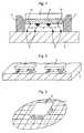
- FIG. 2 The first and second methods are shown in FIG. 2 and FIG 3 illustrates:
- chips 1, 2 are each provided with probe needles 3, brought into contact with pads 4 on a PCB 5 become.
- the second method uses a sample card 6 that is equipped with a large number of such probe needles 3, which in contact with a plurality of chips 1 on one Semiconductor wafers 7 are made of silicon.
- the first method allows the individual to be tested in parallel Chips 1, 2 on the PCB 5, care must be taken that the probe needles 3 each hit their assigned pads 4 and contact them reliably.
- a disadvantage here is that the centering of the individual sample needles on the Pads are difficult to adhere to and that the probe needles continue must be firmly connected to the individual chips, which makes further processing difficult: the test needles can namely practically not removed, so that they the further use of the chips must be taken into account. It’s also a significant expense a complete set of probe needles for each chip realize.
- the second method with the sample card 6 shows the last one mentioned disadvantage of a high expenditure for test needles for not every chip: here the sample card with their Probe needles successively different sets of chips or contact their pads. But it has the disadvantage that a Contacting the chips of an entire semiconductor wafer practically is excluded, because according to the current state of the art the realization of sample cards with some 10,000 individual Trial needles are not possible. But this would be necessary because a semiconductor wafer can have up to 1000 chips can and about 60 sample needles for each of these individual chips are needed, so that a total of the sample card for Testing a wafer or the chips implemented in the wafer 60,000 test needles would be necessary.
- the test needles are not more on the chip, like the first method above, and also no longer on the sample card, as with the above the second method. Rather, the sample needles directly attached to the PCB, so that neither a sample card with the largest possible number of sample needles still sample needles on the individual semiconductor chips are needed.
- the direct attachment of the probe needles to the PCB enables the parallel contacting and testing of a large number of individual chips.
- For testing memory chips in advantageously uses a DIMM-like PCB, because a such PCB testing the memory chip under application conditions allowed.
- interposer can be made of plastic or Plastic and metal exist and is solid with the actual one Chip connected.
- a major advantage of the invention is that in contrast to the prior art according to the above first method the probe needles no longer with the individual Chips are connected. This makes one essential less amount of needles needed because of those on the PCB attached needles for testing the following chips easily can be used.
- the above second usual method must be in the arrangement according to the invention not as exacting requirements as with Sample cards can be made: Through the dummy needles namely a self-centering can be achieved in which by these dummy needles correct adjustment of the sample needles is guaranteed on the pads of the chip or interposer.
- the arrangement according to the invention also allows testing under conditions similar to an actual application the chips. This makes it possible to at safety margins Avoid tests because defective chips are reliably screened out can be.
- a chip is provided with an interposer 8 which in the usual way consists of plastic, in which metal sheets run.
- This interposer 2 can, however, if necessary also be omitted.
- the centering then takes place so that in the uppermost chip layers made of, for example, polyimide and / or silicon dioxide corresponding centering structures be etched.
- FIG. 1 also shows a PCB 5 which, for example, consists of Epoxy resin exists and on the conductor tracks in the usual way run. On these (not shown) conductor tracks or on the surface of the PCB 5 are 9 probe needles at attachment points 3 attached.
- the two in Fig. 1 act entirely outer sample needles that are in recesses 10 of the interposer 8 engage as dummy needles that are not electrically connected for example directly on the surface of the PCB are attached.
- Corresponding leads from these contact pads 12 Conductor tracks through the interposer 8 to the chip 1, see above that its functions can be tested as soon as the probe needles 3 touch the contact pads 12 and thus one Establish electrical connection to a tester, not shown.
- Arrangements as shown in FIG. 1 can be made on the PCB 5 are to be provided side by side in large numbers, so that it is possible to have a large number of chips in parallel at the same time to test on this PCB.
- a tester may be sufficient if the results of the chips lying parallel to one another in a corresponding manner Way to evaluate.
Landscapes
- Physics & Mathematics (AREA)
- General Physics & Mathematics (AREA)
- Engineering & Computer Science (AREA)
- Computer Hardware Design (AREA)
- Microelectronics & Electronic Packaging (AREA)
- Testing Or Measuring Of Semiconductors Or The Like (AREA)
- Measuring Leads Or Probes (AREA)
- Testing Of Individual Semiconductor Devices (AREA)
- Tests Of Electronic Circuits (AREA)
Abstract
Die Erfindung betrifft eine Anordnung zum Testen von Chips
mittels einer gedruckten Schaltungsplatte (PCB) (5), bei der
Probe-Nadeln (3) direkt auf der applikationsnah gestalteten
PCB (5) so angebracht sind, daß auf der PCB (5) mehrere Chips
(1) parallel getestet werden können.

Description
Die vorliegende Erfindung betrifft eine Anordnung zum Testen von Chips, d.h. von in diesen Chips realisierten integrierten Schaltungen, mittels einer gedruckten Schaltungsplatte (PCB = Printed Circuit Board), bei der durch Sonden-Nadeln, bevorzugt auch Probe-Nadeln genannt, eine elektrische Verbindung zwischen der PCB und dem Chip hergestellt wird.The present invention relates to an arrangement for testing of chips, i.e. of integrated in these chips Circuits, by means of a printed circuit board (PCB = Printed Circuit Board), preferred by probe needles also called probe needles, an electrical connection between the PCB and the chip.
Das Testen von Chips wird bevorzugt auf Waferebene vorgenommen, da dort eine Vielzahl von Chips parallel bearbeitet werden kann, was eine erhebliche Zeit- und Kostenersparnis mit sich bringt. In letzter Zeit werden besonders hochparallele Kontaktierungsmethoden, die auf Nadeln mit kleinen Abmessungen basieren und beispielsweise einen Formfaktor berücksichtigen, als erfolgversprechend angesehen. Solche Tests können grundsätzlich mittels zwei verschiedenen Methoden durchgeführt werden:The testing of chips is preferably carried out at the wafer level, because a large number of chips are processed in parallel can what a significant time and cost saving with brings itself. Lately have become particularly parallel Contacting methods based on needles with small dimensions based on a form factor, for example, regarded as promising. Such tests can basically carried out using two different methods become:
Bei der ersten Methode ist eine Anzahl von sehr genauen Probe-Nadeln auf jedem Chip vorgesehen, und diese Probe-Nadeln werden in Kontakt mit Pads bzw. Kontaktkissen auf einer PCB gebracht.The first method uses a number of very accurate probe needles provided on each chip, and these sample needles are in contact with pads or contact pads on a PCB brought.
Bei der zweiten Methode sind die Sonden-Nadeln in großer Anzahl auf einer Sonden- bzw. Probe-Karte angebracht, die zum parallelen Testen mehrerer Chips herangezogen wird.In the second method, the probe needles are in large numbers attached to a probe or sample card, which for parallel testing of multiple chips is used.
Die erste und die zweite Methode sind in der Fig. 2 bzw. der Fig. 3 veranschaulicht:The first and second methods are shown in FIG. 2 and FIG 3 illustrates:
In Fig. 2 sind Chips 1, 2 jeweils mit Probe-Nadeln 3 versehen,
die in Berührung mit Pads 4 auf einer PCB 5 gebracht
werden. 2,
Die zweite Methode verwendet dagegen eine Probe-Karte 6, die
mit einer Vielzahl solcher Probe-Nadeln 3, ausgestattet ist,
welche in Berührung mit einer Vielzahl von Chips 1 auf einem
Halbleiter-Wafer 7 aus Silizium gebracht werden.The second method, on the other hand, uses a
Die erste Methode erlaubt ein paralleles Testen der einzelnen
Chips 1, 2 auf der PCB 5, wobei darauf geachtet werden muß,
daß die Probe-Nadeln 3 jeweils ihre zugeordneten Pads 4 treffen
und diese zuverlässig kontaktieren. Nachteilhaft hierbei
ist, daß die Zentrierung der einzelnen Probe-Nadeln auf die
Pads schwierig einzuhalten ist und daß weiterhin die Probe-Nadeln
fest mit den einzelnen Chips verbunden werden müssen,
was die weitere Verarbeitung erschwert: die Probe-Nadeln können
nämlich praktisch nicht entfernt werden, so daß sie bei
dem weiteren Einsatz der Chips berücksichtigt werden müssen.
Außerdem stellt es einen beträchtlichen Kostenaufwand dar,
für jeden Chip einen vollständigen Satz von Probe-Nadeln zu
verwirklichen.The first method allows the individual to be tested in
Die zweite Methode mit der Probe-Karte 6 weist den zuletzt
genannten Nachteil eines hohen Aufwandes für Probe-Nadeln für
jeden Chip nicht auf: hier kann die Probe-Karte mit ihren
Probe-Nadeln nacheinander verschiedene Sätze von Chips bzw.
deren Pads kontaktieren. Sie hat aber den Nachteil, daß ein
Kontaktieren der Chips eines ganzen Halbleiter-Wafers praktisch
ausgeschlossen ist, da nach derzeitigem Stand der Technik
die Realisierung von Probe-Karten mit einigen 10.000 einzelner
Probe-Nadeln nicht möglich ist. Dies wäre aber erforderlich,
da ein Halbleiter-Wafer bis zu 1000 Chips aufweisen
kann und für jeden von diesen einzelnen Chips etwa 60 Probe-Nadeln
benötigt werden, so daß insgesamt die Probe-Karte zum
Testen eines Wafers bzw. der in dem Wafer realisierten Chips
60.000 Probe-Nadeln notwendig wären. Es braucht auch nicht
besonders betont zu werden, daß ein Arbeiten mit einer derart
großen Anzahl von Probe-Nadeln eine extrem hohe Genauigkeit
in lateraler und senkrechter Richtung, also in der Ebene des
Halbleiter-Wafers und in der zu dieser Ebene senkrechten
Richtung, erfordert.The second method with the
Ausgehend von dem oben aufgezeigten Stand der Technik ist es Aufgabe der vorliegenden Erfindung, eine Anordnung zum Testen von Chips zu schaffen, die ein paralleles Testen einer großen Anzahl von Chips mit Selbstjustierung erlaubt.Based on the prior art shown above, it is Object of the present invention, an arrangement for testing of chips to create a parallel test of a large Number of chips with self-adjustment allowed.
Diese Aufgabe wird bei einer Anordnung der eingangs genannten Art erfindungsgemäß dadurch gelöst, daß die Probe-Nadeln direkt auf der applikationsnah gestalteten PCB so angebracht sind, daß auf der PCB mehrere Chips parallel zu testen sind.This object is achieved with an arrangement of the aforementioned Art solved according to the invention in that the sample needles directly so attached to the application-related PCB are that several chips have to be tested in parallel on the PCB.
Mit diesem Konzept weicht die Erfindung grundsätzlich von dem bisherigen Stand der Technik ab: die Probe-Nadeln sind nicht mehr auf dem Chip, wie bei der obigen ersten Methode, und ebenfalls nicht mehr auf der Probe-Karte, wie bei der obigen zweiten Methode vorgesehen. Vielmehr sind die Probe-Nadeln auf der PCB direkt angebracht, so daß bei der Erfindung weder eine Probe-Karte mit einer möglichst großen Anzahl von Probe-Nadeln noch Probe-Nadeln auf den einzelnen Halbleiterchips benötigt werden. Die PCB selbst sollte dabei möglichst applikationsnah realisiert werden und beispielsweise den späteren Einsatz von Speicherchips auf einem DIMM-Modul (DIMM = Dual-Inline Memory Module) nachbilden.With this concept, the invention differs fundamentally from that previous state of the art: the test needles are not more on the chip, like the first method above, and also no longer on the sample card, as with the above the second method. Rather, the sample needles directly attached to the PCB, so that neither a sample card with the largest possible number of sample needles still sample needles on the individual semiconductor chips are needed. The PCB itself should be as close to the application as possible be realized and for example the later Use of memory chips on a DIMM module (DIMM = Dual Inline Memory module).
Das direkte Anbringen der Probe-Nadeln auf der PCB ermöglicht das parallele Kontaktieren und Testen einer großen Anzahl von einzelnen Chips. Für das Testen von Speicherchips wird in vorteilhafter Weise eine DIMM-ähnliche PCB verwendet, da eine solche PCB das Testen des Speicherchips unter Anwendungsbedingungen erlaubt.The direct attachment of the probe needles to the PCB enables the parallel contacting and testing of a large number of individual chips. For testing memory chips, in advantageously uses a DIMM-like PCB, because a such PCB testing the memory chip under application conditions allowed.
Besonders vorteilhaft ist es, wenn auf der PCB zusätzlich Dummy-Nadeln zur mechanischen Selbstjustierung der Chips angebracht sind. Diese Dummy-Nadeln können dann mit ihren von der PCB abgewandten freien Enden in Markierungen eingreifen, bei denen es sich um Vertiefungen handeln kann, die auf einem mit dem Chip verbundenen Zwischenstück bzw. "Interposer" vorgesehen sind. Ein solcher Interposer kann aus Kunststoff oder Kunststoff und Metall bestehen und ist fest mit dem eigentlichen Chip verbunden.It is particularly advantageous if, in addition, on the PCB Dummy needles for mechanical self-adjustment of the chips attached are. These dummy needles can then be used with their engage the free ends facing away from the PCB, which can be specializations that are based on a provided with the chip intermediate piece or "interposer" are. Such an interposer can be made of plastic or Plastic and metal exist and is solid with the actual one Chip connected.
Ein wesentlicher Vorteil der Erfindung ist darin zu sehen, daß im Gegensatz zu dem Stand der Technik gemäß der obigen ersten Methode die Probe-Nadeln nicht mehr mit den einzelnen Chips verbunden sind. Dadurch ist insgesamt eine wesentlich geringere Menge an Nadeln erforderlich, da die auf der PCB angebrachten Nadeln für das Testen folgender Chips ohne weiteres eingesetzt werden können. Im Gegensatz zu der obigen zweiten üblichen Methode müssen bei der erfindungsgemäßen Anordnung keine so hohen Forderungen an die Genauigkeit wie bei Probe-Karten gestellt werden: Durch die Dummy-Nadeln kann nämlich eine Selbstzentrierung erreicht werden, bei der durch diese Dummy-Nadeln eine korrekte Justierung der Probe-Nadeln auf den Pads des Chips bzw. Interposers gewährleistet wird.A major advantage of the invention is that that in contrast to the prior art according to the above first method the probe needles no longer with the individual Chips are connected. This makes one essential less amount of needles needed because of those on the PCB attached needles for testing the following chips easily can be used. In contrast to the above second usual method must be in the arrangement according to the invention not as exacting requirements as with Sample cards can be made: Through the dummy needles namely a self-centering can be achieved in which by these dummy needles correct adjustment of the sample needles is guaranteed on the pads of the chip or interposer.
Auch erlaubt die erfindungsgemäße Anordnung ein Testen unter ähnlichen Bedingungen wie bei einer tatsächlichen Anwendung der Chips. Dadurch ist es möglich, auf Sicherheitsspannen bei Tests zu verzichten, da fehlerhafte Chips zuverlässig ausgesiebt werden können.The arrangement according to the invention also allows testing under conditions similar to an actual application the chips. This makes it possible to at safety margins Avoid tests because defective chips are reliably screened out can be.
Schließlich besteht ein weiterer Vorteil der erfindungsgemäßen Anordnung darin, daß im Gegensatz zu der obigen herkömmlichen ersten Methode auf aufwendige und genaue Anbringung von Fassungen bzw. Sockets auf der PCB verzichtet werden kann, welche oft anstelle von Pads notwendig sind.Finally, there is another advantage of the invention Arrangement in that unlike the conventional above first method on complex and precise attachment sockets or sockets on the PCB are dispensed with which are often necessary instead of pads.
Nachfolgend wird die Erfindung anhand der Zeichnungen näher erläutert. Es zeigen:
- Fig. 1
- eine erfindungsgemäße Anordnung in einer schematischen Schnittdarstellung,
- Fig. 2
- eine herkömmliche Anordnung, die die erste Methode verwendet, bei welcher Probe-Nadeln an einzelnen Chips angebracht sind, und
- Fig. 3
- eine andere herkömmliche Anordnung, bei welcher Probe-Nadeln an einer Probe-Karte angebracht sind.
- Fig. 1
- an arrangement according to the invention in a schematic sectional view,
- Fig. 2
- a conventional arrangement using the first method in which probe needles are attached to individual chips, and
- Fig. 3
- another conventional arrangement in which probe needles are attached to a probe card.
Die Fig. 2 und 3 sind bereits eingangs erläutert worden. In den Figuren werden einander entsprechende Bauteile jeweils mit den gleichen Bezugszeichen versehen.2 and 3 have already been explained at the beginning. In the figures are corresponding components provided with the same reference numerals.
In Fig. 1 ist ein Chip mit einem Interposer 8 versehen, der
in üblicher Weise aus Kunststoff besteht, in welchem Metallbahnen
verlaufen. Dieser Interposer 2 kann aber gegebenenfalls
auch weggelassen werden. Die Zentrierung erfolgt dann
so, daß in den obersten Chipschichten aus beispielsweise Polyimid
und/oder Siliziumdioxid entsprechende Zentrierungsstrukturen
eingeätzt werden.In Fig. 1, a chip is provided with an
Weiterhin zeigt Fig. 1 eine PCB 5, die beispielsweise aus
Epoxydharz besteht und auf der in üblicher Weise Leiterbahnen
verlaufen. Auf diesen (nicht gezeigten) Leiterbahnen bzw. auf
der Oberfläche der PCB 5 sind an Befestigungsstellen 9 Probe-Nadeln
3 angebracht. Dabei wirken die in Fig. 1 beiden ganz
äußeren Probe-Nadeln, die in Vertiefungen 10 des Interposers
8 eingreifen, als Dummy-Nadeln, die nicht elektrisch angeschlossen,
also beispielsweise direkt auf der Oberfläche der
PCB angebracht sind.1 also shows a
Zentrierhilfen 11, die fest mit der PCB 5 verbunden sind, erlauben
ein Einführen des Chips 1 mit dem Interposer 8, so daß
die Dummy-Nadeln 3 (in Fig. 1 ganz außen) in die Vertiefungen
10 gleiten und den Chip 1 mit dem Interposer 8 genau über den
Probe-Nadeln 3 (in Fig. 1 innen) justieren, wodurch diese
Probe-Nadeln 3 entsprechende Kontaktpads 12 auf dem Interposer
8 kontaktieren. Von diesen Kontaktpads 12 führen entsprechende
Leiterbahnen durch den Interposer 8 zu dem Chip 1, so
daß dieser in seinen Funktionen getestet werden kann, sobald
die Probe-Nadeln 3 die Kontaktpads 12 berühren und damit eine
elektrische Verbindung zu einem nicht gezeigten Tester herstellen.
Anstelle der Vertiefungen 10 können gegebenenfalls auch andere
Markierungen vorgesehen werden, wie beispielsweise in den
oberen Chiplagen aus Polyimid und/oder Siliziumdioxid eingeätzte
Strukturen. Eine derartige Gestaltung kann vorteilhaft
sein, wenn auf den Interposer 8 verzichtet wird und die Kontaktgabe
von den Probe-Nadeln 3 direkt zur Unterseite des
Chips 1 erfolgt.Instead of the
Auf der PCB 5 können Anordnungen, wie diese in Fig. 1 gezeigt
sind, in großer Anzahl nebeneinander vorgesehen werden, so
daß es möglich ist, eine Vielzahl von Chips gleichzeitig parallel
auf dieser PCB zu testen. Für dieses parallele Testen
kann ein Tester ausreichend sein, wenn dieser die Ergebnisse
der parallel zueinander liegenden Chips in entsprechender
Weise auszuwerten vermag.Arrangements as shown in FIG. 1 can be made on the
Claims (5)
dadurch gekennzeichnet, daß die elektrische Verbindung durch direkt auf der PCB (5) angebrachte Probe-Nadeln (3) herstellbar ist und daß auf der PCB (5) zusätzlich als Dummy-Nadeln (3) wirkende Probe-Nadeln zur mechanischen Selbstjustierung der Chips (1) angebracht sind.Arrangement for testing chips (1) by means of a printed circuit board (PCB) (5), in which an electrical connection between the PCB (5) and the chip (1) can be established and testing several chips in parallel on the PCB (5) are,
characterized in that the electrical connection can be established by probe needles (3) attached directly to the PCB (5) and in that probe needles additionally acting as dummy needles (3) for mechanical self-adjustment of the chips ( 1) are attached.
dadurch gekennzeichnet, daß die Dummy-Nadeln (3) mit ihrem von der PCB (5) abgewandten freien Enden in Markierungen eingreifen.Arrangement according to claim 1,
characterized in that the dummy needles (3) engage with their free ends facing away from the PCB (5) in markings.
dadurch gekennzeichnet, daß die Markierungen Vertiefungen (10) sind.Arrangement according to claim 2,
characterized in that the markings are depressions (10).
dadurch gekennzeichnet, daß zwischen den Nadeln (3) und dem Chip (1) ein Zwischenstück (8) vorgesehen ist oder geeignete Strukturen direkt in die Oberfläche des Chips (1) eingebracht sind.Arrangement according to one of claims 1 to 3,
characterized in that an intermediate piece (8) is provided between the needles (3) and the chip (1) or suitable structures are introduced directly into the surface of the chip (1).
dadurch gekennzeichnet, daß die PCB (5) mit Justierhilfen (11) zum Ausrichten der Chips (1) versehen ist.Arrangement according to one of claims 1 to 4,
characterized in that the PCB (5) is provided with adjusting aids (11) for aligning the chips (1).
Applications Claiming Priority (2)
| Application Number | Priority Date | Filing Date | Title |
|---|---|---|---|
| DE19961791A DE19961791C2 (en) | 1999-12-21 | 1999-12-21 | Arrangement for testing chips using a printed circuit board |
| DE19961791 | 1999-12-21 |
Publications (3)
| Publication Number | Publication Date |
|---|---|
| EP1111397A2 true EP1111397A2 (en) | 2001-06-27 |
| EP1111397A3 EP1111397A3 (en) | 2003-06-25 |
| EP1111397B1 EP1111397B1 (en) | 2005-10-26 |
Family
ID=7933661
Family Applications (1)
| Application Number | Title | Priority Date | Filing Date |
|---|---|---|---|
| EP00126789A Expired - Lifetime EP1111397B1 (en) | 1999-12-21 | 2000-12-06 | Means for testing chips using a printed circuit |
Country Status (7)
| Country | Link |
|---|---|
| US (1) | US6472892B2 (en) |
| EP (1) | EP1111397B1 (en) |
| JP (1) | JP2001215256A (en) |
| KR (1) | KR100720788B1 (en) |
| CN (1) | CN1294422C (en) |
| DE (2) | DE19961791C2 (en) |
| TW (1) | TW574507B (en) |
Families Citing this family (15)
| Publication number | Priority date | Publication date | Assignee | Title |
|---|---|---|---|---|
| US6682955B2 (en) * | 2002-05-08 | 2004-01-27 | Micron Technology, Inc. | Stacked die module and techniques for forming a stacked die module |
| US7061126B2 (en) * | 2003-10-07 | 2006-06-13 | Hewlett-Packard Development Company, L.P. | Circuit board assembly |
| JP4525117B2 (en) * | 2004-03-12 | 2010-08-18 | ルネサスエレクトロニクス株式会社 | tray |
| US20070024312A1 (en) * | 2005-07-27 | 2007-02-01 | Atmel Germany Gmbh | Device and method for the testing of integrated semiconductor circuits on wafers |
| US8436636B2 (en) | 2006-10-10 | 2013-05-07 | Apple Inc. | Methods and apparatuses for testing circuit boards |
| US8362793B2 (en) | 2006-11-07 | 2013-01-29 | Apple Inc. | Circuit boards including removable test point portions and configurable testing platforms |
| CN101231322B (en) * | 2007-02-09 | 2011-01-26 | 段超毅 | Test connection method for integrated circuit open circuit/ short-circuit |
| DE102007015283A1 (en) * | 2007-03-29 | 2008-10-02 | Qimonda Ag | Test device for semiconductor devices |
| CN101770967A (en) * | 2009-01-03 | 2010-07-07 | 上海芯豪微电子有限公司 | Test method, device and system of common substrate integrated circuit |
| US8994393B2 (en) | 2012-09-06 | 2015-03-31 | International Business Machines Corporation | High-frequency cobra probe |
| CN104880658B (en) * | 2013-07-23 | 2018-09-07 | 苏州固锝电子股份有限公司 | Test device for acceleration transducer |
| CN105575836B (en) * | 2014-10-08 | 2018-06-12 | 慧荣科技股份有限公司 | Testing device |
| CN105895542A (en) * | 2016-04-20 | 2016-08-24 | 上海斐讯数据通信技术有限公司 | Fixing device and fixing method for chip, PCB and electronic equipment |
| US11761983B2 (en) * | 2021-09-13 | 2023-09-19 | Globalfoundries Singapore Pte. Ltd. | Probe card integrated with a hall sensor |
| CN115542117B (en) * | 2022-09-21 | 2024-01-30 | 深圳市奥高德科技有限公司 | PCB tester capable of synchronously testing multiple units |
Family Cites Families (15)
| Publication number | Priority date | Publication date | Assignee | Title |
|---|---|---|---|---|
| FR2505127A1 (en) * | 1981-04-30 | 1982-11-05 | Moskovic Jacques | Positioning device for locating pins in printed circuit card drilling - has optical reader coinciding centring holes with markers defining pattern to be marked out |
| US5917707A (en) * | 1993-11-16 | 1999-06-29 | Formfactor, Inc. | Flexible contact structure with an electrically conductive shell |
| US6288561B1 (en) * | 1988-05-16 | 2001-09-11 | Elm Technology Corporation | Method and apparatus for probing, testing, burn-in, repairing and programming of integrated circuits in a closed environment using a single apparatus |
| US4924589A (en) * | 1988-05-16 | 1990-05-15 | Leedy Glenn J | Method of making and testing an integrated circuit |
| US5034685A (en) * | 1988-05-16 | 1991-07-23 | Leedy Glenn J | Test device for testing integrated circuits |
| US6336269B1 (en) * | 1993-11-16 | 2002-01-08 | Benjamin N. Eldridge | Method of fabricating an interconnection element |
| US5806181A (en) * | 1993-11-16 | 1998-09-15 | Formfactor, Inc. | Contact carriers (tiles) for populating larger substrates with spring contacts |
| US6064217A (en) * | 1993-12-23 | 2000-05-16 | Epi Technologies, Inc. | Fine pitch contact device employing a compliant conductive polymer bump |
| DE4406538A1 (en) * | 1994-02-28 | 1995-08-31 | Mania Gmbh | Printed circuit board test device with test adapter and method for setting the same |
| JPH085664A (en) * | 1994-06-22 | 1996-01-12 | Hitachi Chem Co Ltd | Inspection board for semiconductor device and its production |
| US5751262A (en) * | 1995-01-24 | 1998-05-12 | Micron Display Technology, Inc. | Method and apparatus for testing emissive cathodes |
| JPH0915262A (en) * | 1995-06-28 | 1997-01-17 | Nec Kansai Ltd | Probe card |
| IT1282617B1 (en) * | 1996-02-13 | 1998-03-31 | Circuit Line Spa | METHOD AND DEVICE FOR THE ELIMINATION OF THE CENTERING ERROR IN THE ELECTRICAL TEST PHASE OF PRINTED CIRCUITS |
| AU3603497A (en) * | 1996-07-05 | 1998-02-02 | Formfactor, Inc. | Floating lateral support for ends of elongate interconnection elements |
| WO1999015908A1 (en) * | 1997-09-19 | 1999-04-01 | Hitachi, Ltd. | Method for manufacturing semiconductor integrated circuit device |
-
1999
- 1999-12-21 DE DE19961791A patent/DE19961791C2/en not_active Expired - Fee Related
-
2000
- 2000-12-06 EP EP00126789A patent/EP1111397B1/en not_active Expired - Lifetime
- 2000-12-06 DE DE50011433T patent/DE50011433D1/en not_active Expired - Lifetime
- 2000-12-18 JP JP2000384321A patent/JP2001215256A/en not_active Withdrawn
- 2000-12-19 KR KR1020000078300A patent/KR100720788B1/en not_active Expired - Fee Related
- 2000-12-20 TW TW89127355A patent/TW574507B/en not_active IP Right Cessation
- 2000-12-21 US US09/745,567 patent/US6472892B2/en not_active Expired - Lifetime
- 2000-12-21 CN CNB001364839A patent/CN1294422C/en not_active Expired - Fee Related
Also Published As
| Publication number | Publication date |
|---|---|
| US20010005141A1 (en) | 2001-06-28 |
| TW574507B (en) | 2004-02-01 |
| CN1294422C (en) | 2007-01-10 |
| EP1111397B1 (en) | 2005-10-26 |
| KR100720788B1 (en) | 2007-05-22 |
| KR20010067427A (en) | 2001-07-12 |
| JP2001215256A (en) | 2001-08-10 |
| DE19961791A1 (en) | 2001-07-12 |
| US6472892B2 (en) | 2002-10-29 |
| CN1316650A (en) | 2001-10-10 |
| DE50011433D1 (en) | 2005-12-01 |
| DE19961791C2 (en) | 2002-11-28 |
| EP1111397A3 (en) | 2003-06-25 |
Similar Documents
| Publication | Publication Date | Title |
|---|---|---|
| DE19837138B4 (en) | Test card for testing chips with integrated circuits | |
| DE4133769C2 (en) | Mounting system for coupling test plates for the recording of electronic components to be tested to a semiconductor test system | |
| DE19961791C2 (en) | Arrangement for testing chips using a printed circuit board | |
| DE69302400T2 (en) | TEST ARRANGEMENT WITH FILM ADAPTER FOR PCB | |
| DE10060438B4 (en) | Test arrangement for parallel testing of a plurality of integrated circuits and test methods | |
| DE112006001477B4 (en) | Probe card | |
| DE102004028185A1 (en) | test card | |
| DE2525166A1 (en) | CONTACT PROBE DEVICE | |
| DE19507127A1 (en) | Adapter system for component boards, to be used in a test facility | |
| EP0838688B1 (en) | Device and procedure for testing printed circuit boards | |
| DE10153666B4 (en) | High density contact assembly and method of arranging contacts | |
| DE10228291B4 (en) | Semiconductor device socket | |
| DE2547323C3 (en) | Carrier plate for at least one integrated semiconductor storage | |
| EP0278073B1 (en) | Probe for an adapter for a device for testing printed circuit boards | |
| EP0875767B1 (en) | Device and procedure for testing naked circuit boards | |
| DE19931278B4 (en) | Test card and IC tester | |
| DE10060585A1 (en) | Device and method for examining a semiconductor integrated circuit | |
| DE102004034357A1 (en) | Test cards carrier element | |
| EP1031042B1 (en) | Device for testing printed boards | |
| DE69430036T2 (en) | Test device for integrated circuits | |
| DE2753236C2 (en) | Installation frame for an integrated semiconductor circuit arrangement without a housing | |
| EP1162655A2 (en) | Integrated circuit device for testing of transistors and semiconductor wafer equipped with such a circuit device | |
| DE10135517A1 (en) | Land grid array package mounting apparatus for testing semiconductor device package, has cam for moving bending plate and for bending each contact finger which passes through the bending plate | |
| DE10128378A1 (en) | Mounting apparatus for high frequency, electronic device package, has electrically insulated guide plate with inner and outer guide hole sets secured on support base | |
| DE102020116233A1 (en) | Circuit carrier with connection area field and method for producing a connection area field on a circuit carrier |
Legal Events
| Date | Code | Title | Description |
|---|---|---|---|
| PUAI | Public reference made under article 153(3) epc to a published international application that has entered the european phase |
Free format text: ORIGINAL CODE: 0009012 |
|
| AK | Designated contracting states |
Kind code of ref document: A2 Designated state(s): AT BE CH CY DE DK ES FI FR GB GR IE IT LI LU MC NL PT SE TR |
|
| AX | Request for extension of the european patent |
Free format text: AL;LT;LV;MK;RO;SI |
|
| PUAL | Search report despatched |
Free format text: ORIGINAL CODE: 0009013 |
|
| AK | Designated contracting states |
Designated state(s): AT BE CH CY DE DK ES FI FR GB GR IE IT LI LU MC NL PT SE TR |
|
| AX | Request for extension of the european patent |
Extension state: AL LT LV MK RO SI |
|
| 17P | Request for examination filed |
Effective date: 20031211 |
|
| AKX | Designation fees paid |
Designated state(s): DE FR GB IE IT |
|
| 17Q | First examination report despatched |
Effective date: 20040209 |
|
| GRAP | Despatch of communication of intention to grant a patent |
Free format text: ORIGINAL CODE: EPIDOSNIGR1 |
|
| GRAS | Grant fee paid |
Free format text: ORIGINAL CODE: EPIDOSNIGR3 |
|
| GRAA | (expected) grant |
Free format text: ORIGINAL CODE: 0009210 |
|
| AK | Designated contracting states |
Kind code of ref document: B1 Designated state(s): DE FR GB IE IT |
|
| PG25 | Lapsed in a contracting state [announced via postgrant information from national office to epo] |
Ref country code: IT Free format text: LAPSE BECAUSE OF FAILURE TO SUBMIT A TRANSLATION OF THE DESCRIPTION OR TO PAY THE FEE WITHIN THE PRESCRIBED TIME-LIMIT;WARNING: LAPSES OF ITALIAN PATENTS WITH EFFECTIVE DATE BEFORE 2007 MAY HAVE OCCURRED AT ANY TIME BEFORE 2007. THE CORRECT EFFECTIVE DATE MAY BE DIFFERENT FROM THE ONE RECORDED. Effective date: 20051026 |
|
| REG | Reference to a national code |
Ref country code: GB Ref legal event code: FG4D Free format text: NOT ENGLISH |
|
| REG | Reference to a national code |
Ref country code: IE Ref legal event code: FG4D Free format text: LANGUAGE OF EP DOCUMENT: GERMAN |
|
| REF | Corresponds to: |
Ref document number: 50011433 Country of ref document: DE Date of ref document: 20051201 Kind code of ref document: P |
|
| GBT | Gb: translation of ep patent filed (gb section 77(6)(a)/1977) |
Effective date: 20060119 |
|
| PLBE | No opposition filed within time limit |
Free format text: ORIGINAL CODE: 0009261 |
|
| STAA | Information on the status of an ep patent application or granted ep patent |
Free format text: STATUS: NO OPPOSITION FILED WITHIN TIME LIMIT |
|
| 26N | No opposition filed |
Effective date: 20060727 |
|
| EN | Fr: translation not filed | ||
| PG25 | Lapsed in a contracting state [announced via postgrant information from national office to epo] |
Ref country code: FR Free format text: LAPSE BECAUSE OF FAILURE TO SUBMIT A TRANSLATION OF THE DESCRIPTION OR TO PAY THE FEE WITHIN THE PRESCRIBED TIME-LIMIT Effective date: 20061215 |
|
| PGFP | Annual fee paid to national office [announced via postgrant information from national office to epo] |
Ref country code: GB Payment date: 20061221 Year of fee payment: 7 |
|
| GBPC | Gb: european patent ceased through non-payment of renewal fee |
Effective date: 20071206 |
|
| PG25 | Lapsed in a contracting state [announced via postgrant information from national office to epo] |
Ref country code: FR Free format text: LAPSE BECAUSE OF FAILURE TO SUBMIT A TRANSLATION OF THE DESCRIPTION OR TO PAY THE FEE WITHIN THE PRESCRIBED TIME-LIMIT Effective date: 20051231 |
|
| PG25 | Lapsed in a contracting state [announced via postgrant information from national office to epo] |
Ref country code: FR Free format text: LAPSE BECAUSE OF FAILURE TO SUBMIT A TRANSLATION OF THE DESCRIPTION OR TO PAY THE FEE WITHIN THE PRESCRIBED TIME-LIMIT Effective date: 20051026 |
|
| PG25 | Lapsed in a contracting state [announced via postgrant information from national office to epo] |
Ref country code: GB Free format text: LAPSE BECAUSE OF NON-PAYMENT OF DUE FEES Effective date: 20071206 |
|
| PGFP | Annual fee paid to national office [announced via postgrant information from national office to epo] |
Ref country code: IE Payment date: 20141222 Year of fee payment: 15 |
|
| PGFP | Annual fee paid to national office [announced via postgrant information from national office to epo] |
Ref country code: DE Payment date: 20150129 Year of fee payment: 15 |
|
| REG | Reference to a national code |
Ref country code: DE Ref legal event code: R081 Ref document number: 50011433 Country of ref document: DE Owner name: INFINEON TECHNOLOGIES AG, DE Free format text: FORMER OWNER: QIMONDA AG, 81739 MUENCHEN, DE Ref country code: DE Ref legal event code: R081 Ref document number: 50011433 Country of ref document: DE Owner name: POLARIS INNOVATIONS LTD., IE Free format text: FORMER OWNER: QIMONDA AG, 81739 MUENCHEN, DE |
|
| REG | Reference to a national code |
Ref country code: DE Ref legal event code: R081 Ref document number: 50011433 Country of ref document: DE Owner name: POLARIS INNOVATIONS LTD., IE Free format text: FORMER OWNER: INFINEON TECHNOLOGIES AG, 85579 NEUBIBERG, DE |
|
| REG | Reference to a national code |
Ref country code: DE Ref legal event code: R119 Ref document number: 50011433 Country of ref document: DE |
|
| REG | Reference to a national code |
Ref country code: IE Ref legal event code: MM4A |
|
| PG25 | Lapsed in a contracting state [announced via postgrant information from national office to epo] |
Ref country code: DE Free format text: LAPSE BECAUSE OF NON-PAYMENT OF DUE FEES Effective date: 20160701 Ref country code: IE Free format text: LAPSE BECAUSE OF NON-PAYMENT OF DUE FEES Effective date: 20151206 |