EP1110232B1 - Automated set up of an energy filtering transmission electron microscope - Google Patents
Automated set up of an energy filtering transmission electron microscope Download PDFInfo
- Publication number
- EP1110232B1 EP1110232B1 EP99967841A EP99967841A EP1110232B1 EP 1110232 B1 EP1110232 B1 EP 1110232B1 EP 99967841 A EP99967841 A EP 99967841A EP 99967841 A EP99967841 A EP 99967841A EP 1110232 B1 EP1110232 B1 EP 1110232B1
- Authority
- EP
- European Patent Office
- Prior art keywords
- magnification
- average
- scanned beam
- energy filtering
- aspect ratio
- Prior art date
- Legal status (The legal status is an assumption and is not a legal conclusion. Google has not performed a legal analysis and makes no representation as to the accuracy of the status listed.)
- Expired - Lifetime
Links
- 238000001914 filtration Methods 0.000 title claims description 142
- 230000005540 biological transmission Effects 0.000 title claims description 34
- 238000000034 method Methods 0.000 claims description 49
- 230000004075 alteration Effects 0.000 claims description 47
- 230000000694 effects Effects 0.000 claims description 27
- 238000005259 measurement Methods 0.000 claims description 24
- 238000006073 displacement reaction Methods 0.000 claims description 23
- 238000010894 electron beam technology Methods 0.000 claims description 19
- 230000003287 optical effect Effects 0.000 claims description 10
- 230000003466 anti-cipated effect Effects 0.000 claims description 6
- 238000004891 communication Methods 0.000 claims description 3
- 238000001228 spectrum Methods 0.000 description 42
- 230000008859 change Effects 0.000 description 33
- 230000007547 defect Effects 0.000 description 11
- 238000012937 correction Methods 0.000 description 10
- 238000005286 illumination Methods 0.000 description 7
- 230000007246 mechanism Effects 0.000 description 4
- 238000004458 analytical method Methods 0.000 description 3
- 238000013459 approach Methods 0.000 description 3
- 238000004364 calculation method Methods 0.000 description 3
- 238000003384 imaging method Methods 0.000 description 3
- 230000001143 conditioned effect Effects 0.000 description 2
- 238000000286 energy filtered transmission electron microscopy Methods 0.000 description 2
- 238000005516 engineering process Methods 0.000 description 2
- 238000012986 modification Methods 0.000 description 2
- 230000004048 modification Effects 0.000 description 2
- 238000012546 transfer Methods 0.000 description 2
- 101100063432 Caenorhabditis elegans dim-1 gene Proteins 0.000 description 1
- 101100499346 Caenorhabditis elegans dld-1 gene Proteins 0.000 description 1
- 230000001133 acceleration Effects 0.000 description 1
- 230000009471 action Effects 0.000 description 1
- 238000003491 array Methods 0.000 description 1
- 230000009286 beneficial effect Effects 0.000 description 1
- 238000001514 detection method Methods 0.000 description 1
- 239000006185 dispersion Substances 0.000 description 1
- 230000005672 electromagnetic field Effects 0.000 description 1
- 230000010354 integration Effects 0.000 description 1
- 230000001788 irregular Effects 0.000 description 1
- 239000011159 matrix material Substances 0.000 description 1
- 239000002184 metal Substances 0.000 description 1
- 238000011017 operating method Methods 0.000 description 1
- 230000008520 organization Effects 0.000 description 1
- 230000000737 periodic effect Effects 0.000 description 1
- 230000008569 process Effects 0.000 description 1
- 238000012545 processing Methods 0.000 description 1
- 230000000750 progressive effect Effects 0.000 description 1
- 238000011160 research Methods 0.000 description 1
- 230000035945 sensitivity Effects 0.000 description 1
- 238000004627 transmission electron microscopy Methods 0.000 description 1
Images


Classifications
-
- H—ELECTRICITY
- H01—ELECTRIC ELEMENTS
- H01J—ELECTRIC DISCHARGE TUBES OR DISCHARGE LAMPS
- H01J37/00—Discharge tubes with provision for introducing objects or material to be exposed to the discharge, e.g. for the purpose of examination or processing thereof
- H01J37/252—Tubes for spot-analysing by electron or ion beams; Microanalysers
-
- H—ELECTRICITY
- H01—ELECTRIC ELEMENTS
- H01J—ELECTRIC DISCHARGE TUBES OR DISCHARGE LAMPS
- H01J37/00—Discharge tubes with provision for introducing objects or material to be exposed to the discharge, e.g. for the purpose of examination or processing thereof
- H01J37/02—Details
- H01J37/04—Arrangements of electrodes and associated parts for generating or controlling the discharge, e.g. electron-optical arrangement or ion-optical arrangement
- H01J37/05—Electron or ion-optical arrangements for separating electrons or ions according to their energy or mass
-
- H—ELECTRICITY
- H01—ELECTRIC ELEMENTS
- H01J—ELECTRIC DISCHARGE TUBES OR DISCHARGE LAMPS
- H01J37/00—Discharge tubes with provision for introducing objects or material to be exposed to the discharge, e.g. for the purpose of examination or processing thereof
- H01J37/26—Electron or ion microscopes; Electron or ion diffraction tubes
- H01J37/261—Details
- H01J37/265—Controlling the tube; circuit arrangements adapted to a particular application not otherwise provided, e.g. bright-field-dark-field illumination
-
- H—ELECTRICITY
- H01—ELECTRIC ELEMENTS
- H01J—ELECTRIC DISCHARGE TUBES OR DISCHARGE LAMPS
- H01J2237/00—Discharge tubes exposing object to beam, e.g. for analysis treatment, etching, imaging
- H01J2237/244—Detection characterized by the detecting means
- H01J2237/24485—Energy spectrometers
-
- H—ELECTRICITY
- H01—ELECTRIC ELEMENTS
- H01J—ELECTRIC DISCHARGE TUBES OR DISCHARGE LAMPS
- H01J2237/00—Discharge tubes exposing object to beam, e.g. for analysis treatment, etching, imaging
- H01J2237/245—Detection characterised by the variable being measured
- H01J2237/24571—Measurements of non-electric or non-magnetic variables
- H01J2237/24585—Other variables, e.g. energy, mass, velocity, time, temperature
-
- H—ELECTRICITY
- H01—ELECTRIC ELEMENTS
- H01J—ELECTRIC DISCHARGE TUBES OR DISCHARGE LAMPS
- H01J2237/00—Discharge tubes exposing object to beam, e.g. for analysis treatment, etching, imaging
- H01J2237/26—Electron or ion microscopes
- H01J2237/282—Determination of microscope properties
- H01J2237/2826—Calibration
Definitions
- the invention of the present application relates in general to energy filtering transmission electron microscopes and, more particularly, to an automated adjustment or set up of energy filtering systems of energy filtering transmission electron microscopes.
- Modem energy filtering transmission electron microscopes are able to form images from energy resolved subsets of an electron beam which has traversed a specimen.
- the images produced by energy filtering microscopes will be aberrated and distorted unless optical defects inherent to an energy dispersing element of an energy filtering system are precisely compensated by additional electron lenses within the energy filtering system. Making the needed adjustments is a task requiring a high level of theoretical knowledge and experimental skill which restricts the availabitity of modem EFTEMs to a handful of experts.
- a mask which forms a patterned aperture array.
- a mask of known geometry and dimensions is selectively inserted at the entrance to the energy filtering system by means of an entrance aperture assembly.
- the mask preferably comprises an array of fine, laser drilled holes.
- a computer captures the image of the mask with an electron camera and determines the location of the center of each hole within the image. The displacement of the location of each hole position of the mask image from its anticipated position with perfectly adjusted optics, is measured, processed and converted by the computer into correcting adjustments.
- WO 98/06125 teaches a system for adjusting an EFTEM by inserting a mask of known geometry at the entrance of the energy filter of the device and making subsequent adjustments based upon the detected image of the mask.
- a mask of known geometry at the entrance of the energy filter of the device and making subsequent adjustments based upon the detected image of the mask.
- filter aberrations can be assessed without such a mask.
- Optics of the electron microscope preceding an energy filter are used to scan the beam at the entrance to the filter in a pattern corresponding to a defined geometry.
- the beam can either be finely focused to yield a spot at each position visited during the pattern scan, or the beam can be spread out and imprinted with a well-defined intensity distribution, such as normally occurs due to passage of the beam through a specimen, so that its relative scanned displacements can be assessed using cross-correlation techniques.
- the finely focused beam electron images of the scanned pattern, as recorded at some point beyond the energy filter, directly yield a spot pattern image. Deviations of the recorded spot pattern image from the defined scan geometry reflect the imaging aberrations introduced by the energy filter.
- post-filter electron images of the scanned beam are cross-correlated with an image of the beam taken without scanning, i.e, an undeflected beam image, yielding cross-correlation peak images that give the effective displacement of each scanned beam position due to the aberrations/distortions of the filter.
- Summing the cross-correlation peak images again yields a spot pattern image that is equivalent to that obtained in the focused beam case. Deviations of the recorded spot pattern image from the defined scan geometry are analyzed to assess and subsequently correct aberrations introduced by the energy filter.
- Optics of the electron microscope preceding an energy filter are used to finely focus or spread the beam at the entrance to the filter with the beam then being scanned in a pattern corresponding to a defined geometry with the scanned beam images being used to determine points of relative scanned displacement.
- an offset is applied to the energies of the beam electrons by changing the accelerating voltage at an electron gun of the transmission electron microscope (TEM).
- TEM transmission electron microscope
- the known positions of the scanned beam image are again located and the differences between the current positions and those measured before the change in beam energy are determined. The differences are averaged and the net average displacement is taken as a measure of the energy filtering system's departure from true achromatic imaging.
- the effect on average displacement to changes in the current of a chromatic adjustment quadrupole lens of post-slit electron optics of the energy filtering system is assessed.
- the current in the chromatic adjustment quadrupole lens is changed and the measurement of net average displacement of scanned beam image positions is repeated.
- the scanned beam image positions are located.
- the average distance between positions along the top and bottom of the scanned beam image is determined and the average distance between positions along the right and left sides of the scanned beam image is determined with these two distances being used to calculate the overall magnification, M, of the image, and the ratio of the vertical to the horizontal magnification is utilized to obtain the aspect ratio, A, of the image.
- the incremental effects on M and A of currents flowing through first and second magnification adjusting quadrupole lenses of the post-slit electron optics of the energy filtering system are computed and used to determine current changes which are applied to the magnification adjusting quadrupole lenses.
- the measurements of M and A are repeated and, if the measured values still deviate from preferred values by more than operator specified tolerances, the entire procedure, starting with the controlled changes to the quadrupole currents, is iterated until the specified tolerances are met.
- An image of the scanned beam is captured by an electron camera and the location of the center of each scanned beam illumination within the image is determined.
- the position data is analyzed relative to nominal positions using least squares fits, one for horizontal measured coordinates and the other for vertical measured coordinates.
- Aberration coefficients are determined and nullified by adjustments to currents passing through three sextupole lenses of post-slit electron optics of the energy filtering system.
- an object of the present invention to provide an autoadjustment set up method and apparatus for an energy filtering transmission electron microscope which can adjust an energy filtering system of the microscope using images of strategically placed scanned beam illumination without the need of additional masks, apertures, lenses or the like; to provide an autoadjustment set up method and apparatus for an energy filtering transmission electron microscope which can adjust an energy filtering system of the microscope to consistently achieve and exceed required precision for the adjustments; and, to provide an autoadjustment set up method and apparatus for an energy filtering transmission electron microscope which can adjust an energy filtering system of the microscope with computational demands which can be met by a conventional personal computer interfaced to energy filtering system hardware.
- a method for automatically performing set up adjustments for an energy filtering transmission electron microscope to correct electron optical aberrations of an energy filtering system of said microscope comprising the steps of:
- said electron beam is finely focused. It is also preferred that said step of analyzing said electron images of said scanned beam comprises the steps of:
- said step of analyzing said electron images of said scanned beam comprises the steps of:
- said step of analyzing said electron images of said scanned beam may comprise the steps of:
- the steps of determining first, second and third average vertical magnifications; first, second and third average horizontal magnifications; and, first, second and third average aspect ratios of an electron image of said scanned beam comprise the steps of:
- said steps of analyzing said electron images of said scanned beam and applying said adjustments to said energy filtering system may comprise the steps of:
- said steps of analyzing said electron images of said scanned beam and applying said adjustments to said energy filtering system may comprise the steps of:
- said electron beam is spread and said method further comprises the steps of:
- said step of analyzing said electron images of said scanned beam comprises the steps of:
- said step of analyzing said electron images of said scanned beam may comprise the steps of:
- the steps of determining first, second and third average vertical magnifications; first, second and third average horizontal magnifications; and, first, second and third average aspect ratios of an electron image of said scanned beam comprise the steps of:
- said steps of analyzing said electron images of said scanned beam and applying said adjustments to said energy filtering system may comprise the steps of:
- said steps of analyzing said electron images of said scanned beam and applying said adjustments to said energy filtering system may comprise the steps of:
- a method for automatically performing set up adjustments for an energy filtering transmission electron microscope as previously described wherein said electron beam is scanned in said known geometric pattern within a time allotted to a single exposure of said beam detector such that an electron image of said scanned beam defines a spot pattern image of said geometric pattern scanned by said electron beam within said allotted time.
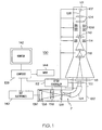
- Fig. 1 is a schematic side view of an energy filtering transmission electron microscope (EFTEM) system 100 operable in accordance with the present invention.
- the EFTEM system 100 includes a transmission electron microscope (TEM) 101 which comprises an electron gun 102, condenser lenses 104 and an illumination deflector system 106 which together focus a beam of electrons 108 onto a thin sample 110.
- the beam of electrons 108 thus focused upon the sample 110 are mono-energetic, i.e., all the electrons in the beam have the same energy which is determined by an accelerating voltage applied to the electron gun 102 under the control of an EFTEM controller 112.
- the beam energy or the energy supplied to each beam electron as a result of the accelerating voltage has an operator-selected value in the range of about 40,000 to about 2,000,000 electron-volts (eVs) with a typical tolerance of ⁇ 1 eV.
- Electrons transmitted through the sample 110 form an image which is magnified by an objective lens 114, aligned with an optic axis of the projector lens system by shift coils 115, 117 and further magnified by projector lenses 116.
- the beam electrons interact with the sample 110 by a variety of mechanisms, thereby transferring varying amounts of energy to the sample 110.
- the energy transfers termed energy losses in the field of transmission electron microscopy, alter the distribution of electron energies present in the image at all points beyond the sample 110 or specimen plane. Accordingly, the transmitted image no longer consists of mono-energetic electrons, but rather of electrons with energies that have been reduced in energy by anywhere between zero and several thousand eVs relative to the initial acceleration energy.
- a portion of the transmitted electron image is passed through an entrance aperture assembly 118 of an energy filtering system 120, conditioned by pre-slit optics 122, and passed through an electron prism or energy dispersing element 124.
- the entrance aperture assembly 118 is controlled by a computer 126 to position one of a number of different filter entrance apertures to intercept the beam or to retract the apertures fully to permit the entire beam to enter the filtering system 120.
- Three or four aperture sizes or shapes are commonly used; however, any reasonable number of apertures can be provided for a given EFTEM.
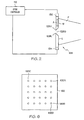
- the pre-slit optics 122 and the dispersing element 124 act upon the beam to produce a beam intensity profile P at the plane of an energy-selecting slit assembly 128, which defines a slit opening 128S and a beam detector made up by current detectors 132, 134 of Fig. 2 .
- One of the two orthogonal spatial dimensions of the beam or rather beam image is reduced to have a very narrow spatial width and, in its place, the beam electron energy losses are dispersed along that dimension, as suggested in Figs. 1 and 2 , to form an energy loss spectrum at the energy selecting slit assembly 128.
- the dispersion of the energy loss spectrum has a value in the range of 1 to 10 micrometers ( ⁇ m) per eV.
- the energy loss spectrum or beam intensity profile P is oriented such that the energy loss dimension is in the plane of Figs. 1 and 2 and directed across or transverse to upper and lower knife edges 128U, 128L of the energy-selecting slit assembly 128 as shown in Fig. 2 .
- the range of electron energies permitted to contribute to the electron image at all points beyond the plane of the energy-selecting slit assembly 128, especially at a beam detector assembly 130, is thus controlled by the size of the slit opening 128S and the positioning of the zero energy loss portion of the spectrum, which is termed the zero loss peak in the field of energy filtered transmission electron microscopy, with respect to the center of the slit opening 128S.
- a typical transmission sample 110 has a thickness so small that the zero loss peak is the most prominent feature of the spectrum, comprising at a minimum 5%, but more typically 30% or more, of the total spectrum intensity.
- the position of the zero loss peak with respect to the center of the slit opening 128S is controlled by two independent instrument parameters, the accelerating voltage at the electron gun 102 and the control current passing through the dispersing element 124, both of which can be controlled by the EFTEM controller 112 or by the computer 126 through the EFTEM controller 112.
- the energy selecting slit assembly 128 is also controlled by the EFTEM controller 112 or by the computer 126 through the EFTEM controller 112 to select the size of a desired slit opening 128S, as indicated by an arrow A in Fig. 2 , and also the positioning of the slit assembly 128, i.e., having a slit mechanism inserted into the beam path or entirely retracted from the beam path.
- the slit assembly 128 can be controlled to vary the size of the slit opening 128S from less 30 than 1 ⁇ m (micron), fully closed and approximating 0 ⁇ m, to about 300 ⁇ m. For a range of slit openings from about 0 ⁇ m to about 150 ⁇ m, the slit passes electrons having a range of energies from about 0 eV to about 75 eV.
- Any portion of the energy-dispersed beam intensity profile P intercepted by an upper portion U of the slit assembly 128 which defines the slit opening 128S is converted to a signal proportional to the intercepted beam current by the current detector 132 and is read by the computer 126. Any portion of the energy-dispersed beam intensity profile P intercepted by the lower portion L of the slit assembly 128 which defines the slit opening 128S is converted to a signal proportional to the intercepted beam current by the current detector 134 and is also read by the computer 126.
- the slit mechanism of the slit assembly 128 may also be fully retracted from the beam path, for example by the computer 126 via the EFTEM controller 112, for example when it is desired to have all energy losses contribute to an electron image formed beyond the plane of the slit assembly 128.
- the electron image is further conditioned by post-slit optics 136, and ultimately projected as a final image 138 onto the beam detector assembly 130.
- the beam detector assembly 130 transforms the electron image 138 into a series of signals which are sent to detector electronics 140, where the signals are processed and transmitted to the computer 126.
- the beam detector assembly 130 may comprise an electron camera and preferably a slow scan CCD camera that converts the electron image 138 into a light image in a thin scintillator, transmits the light image to a scientific-grade slow-scan CCD chip, reads and digitizes the image to have high sensitivity and dynamic range, and transmits the image to the computer 126 over a digital interface.
- cameras giving immediate electronic readout can also be used, such as TV-rate cameras adapted for the detection of electron images, 1-dimension detectors that detect images by scanning them over the detector in a transverse direction and even single-channel detectors that detect images by scanning them over the detector in two different directions.
- the computer 126 is equipped with a monitor 142 for displaying images and other data, and an input device 144 such as a keyboard, mouse, or a trackball for accepting user input.
- the computer 126 has communication links to the entire microscope/filtering system 101, 120 via the EFTEM controller 112, and is able to control all salient elements of the EFTEM system 100, including the accelerating voltage of the electron gun 102, the entrance aperture assembly 118, the pre-slit optics 122, the energy dispersing element 124, the slit assembly 128, the post-slit optics 136 and the beam detector assembly 130.
- a Castaing-Henry filter for use in the TEM 101 is described by Castaing et al. in Comptes Rendus d'Académie des Sciences (Paris), vol. 255, pp. 76-78 (1962 ); and, the action of sextupote lenses included in the EFTEM system 100 can be understood using the beam matrix approach described by Brown et al. in the report 80-04 published by the European Organization for Nuclear Research in Geneva, Switzerland (1980).
- the invention of the present application automatically performs the adjustments needed to set up EFTEMs for effective usage so that the EFTEMs are adjusted to correct for electron optical aberrations of the energy filtering system 120 which would otherwise be present.
- the invention will be described relative to a series of procedures, shown in Fig. 3 . each of which performs a beneficial adjustment for set up of the EFTEM with the procedures tending to be progressive in that, as the series progresses, the procedures achieve higher levels of refinement of the adjustment of the electron optics of the energy filtering system 120.
- each level of refinement corrects aberrations of the Nth order, where N ranges from 0 to an upper limit constrained primarily by practical limitations of electron optical technology.
- Aberrations of the lowest or 0th order involve lateral misalignments or displacements of the electron beam from a desired trajectory generally along an optical axis of the instrument.
- the most critical alignment is that of the energy-dispersed beam through the slit opening 128S of the energy selecting slit assembly 128.
- correction of 0th order aberrations requires precise adjustment of the control current passing through the dispersing element 124 so that a known reference point, such as the zero loss peak, within the energy-dispersed beam or energy loss spectrum formed at the plane of the slit assembly 128 passes through the center of the slit opening 128S, see 150 Figs. 3 and 4 .
- the automated adjustment for set up of the EFTEM to correct for 0th order aberrations is performed by first determining the approximate location of the energy-dispersed beam. First the entrance aperture assembly 118 and the slit assembly 128 are operated by the computer 126 to retract both from the beam path. The output image 138 captured by the beam detector assembly 130 or electron camera is read by the computer 126 and the intensities of all pixels of the output image 138 are summed to obtain a single numeric value proportional to the total electron beam intensity in the image 138, see block 152. Next, the slit assembly 128 is inserted into the beam path and the beam intensity of the resulting output image 138 is measured as before, see block 154.
- the total electron beam intensity with the slit inserted into the beam path is divided by the total electron beam intensity with the slit removed from the beam path to determine a ratio which represents the percentage of the energy-dispersed beam which passes through the slit opening 128S, see block 156.
- the ratio is compared to a selected percentage, for example ranging from about 10% to about 50% with 25% being selected for a working embodiment, see block 158.
- the ratio is at least 25% or at least the selected percentage, the zero loss peak of the energy loss spectrum is deemed to be coarsely aligned in the approximate vicinity of the slit opening 128S and the adjustment process proceeds to the next one of the series of adjustment procedures. If the ratio does not meet the selected percentage criterion, coarse alignment is performed by reading the beam current signals generated at the slit assembly 128 by the upper-slit beam current detector 132 and the lower-slit beam current detector 134, see block 160. The two beam current signals are compared to one another to determine whether the majority of the spectrum intensity falls on the upper slit half or on the lower slit half, see block 162.
- the control current passing through the dispersing element 124 is adjusted to move the zero loss peak away from the slit half with the higher beam current signal until the readings from the currents detectors 132, 134 are substantially balanced, see block 164, at which point adjustment of the zero loss peak of the energy loss spectrum is deemed to be coarsely aligned with the slit opening 128S.
- fine centering of the zero loss peak within the slit opening 128S is performed by locating the zero loss peak relative to the upper knife edge 128U of the energy-selecting slit assembly 128.
- the control current passing through the dispersing element 124 is adjusted to move the energy loss spectrum towards the upper slit half U until the beam intensity of the output image 138 captured by the beam detector assembly 130 is measured to be substantially zero, see blocks 166, 168, 170.
- control current passing through the dispersing element 124 is then adjusted in the reverse direction to move the energy loss spectrum toward the slit opening 128S in discrete steps ranging, for example, from about 0.1 eV to about 5 eV with 1 eV being used for a working embodiment, see block 172.
- the beam intensity in the output image 138 is measured at each step by the computer 126 via the beam detector assembly 130, see block 174.
- the difference between the just-measured intensity reading and the immediately preceding measured intensity is determined, see block 176.
- the energy loss spectrum is stepped until the current difference is smaller than the preceding one, i.e., until a peak intensity or maximum in the incremental intensity in the image 138 has been detected, see blocks 178, 180.
- the zero loss peak is deemed to have just passed the upper knife edge 128U and to therefore be positioned at the knife edge to within a precision of one step, for example 1 eV.
- the control current passing through the dispersing element 124 is then changed to move the zero loss peak toward the center of the slit opening 128S by an amount precisely equal to one half the slit width, see block 182.
- This precision control current change is possible because the computer 126 has calibrated information about the size of the slit opening 128S in eVs as well as calibrated information about the effect of control current changes to the dispersing element 124 in terms of energy loss spectrum displacements in eVs. While fine centering of the zero loss peak within the slit opening 128S could be performed directly as described without the coarse alignment, the initial coarse alignment greatly speeds up the entire alignment/centering procedure.
- the parameters of the electron optics of the energy filtering system 120 which are adjusted to correct the 1st order aberrations are: the degree to which components of the image formed with beam electrons of different energies are in perfect registration with each other, termed the achromaticity of the image, see block 186; the size, in both horizontal and vertical dimensions, of the image 138 formed at the beam detector assembly 130, termed the magnification and aspect ratio of the image 138, see block 188; and, the degree to which spatial information along the energy dimension of the energy loss spectrum formed at the slit assembly 128 has truly been demagnified to a vanishing spatial extent, termed the focus of the spectrum, see block 190.
- the achromaticity of the image 138 is adjusted by varying a current, Ich, passing through a chromatic adjustment quadrupole lens that is part of the post-slit optics 136.
- the magnification and aspect ratio of the image 138 formed at the beam detector assembly 130 are adjusted by varying currents, Im1 and Im2, passing through two additional independent magnification adjusting quadrupole lenses that are also part of the post-slit optics 136.
- the focus of the energy loss spectrum formed at energy-selecting slit assembly 128 is adjusted by varying currents, Ifx and Ify, passing through two independent spectrum-focusing quadrupole lenses that are part of the pre-slit optics 122.
- the achromaticity, magnification and aspect ratio of electron image 138 formed at the beam detector assembly 130 are assessed using the beam scanning capabilities of the TEM optics.
- the electron microscope optics that precede the energy filtering system 120 are used to finely focus the beam at the entrance to the filter, thus forming a well-defined ray of illumination.
- the beam thus formed is then scanned or deflected in a pattern of known geometry and dimension.
- the electron images of the scanned finely focused beam form spot pattern images.
- the spot pattern defines a beam intensity distribution wherein the center of the beam intensity distribution is successively placed at discrete positions.
- An image of the patterned beam scan is then formed at the beam detector assembly 130 or electron camera.
- a large variety of patterns can be used in the present invention with preferred forms of patterns defining discrete points of centered beam intensity distribution and having spacing between those points such that the points and spacing can be easily determined from the patterned beam scan image by the computer 126.
- preferred forms of patterns are most easily included with the operating procedures performed by the computer 126, many other forms can be used but will require more effort in terms of programming the computer 126.
- a particularly advantageous pattern comprises a square array wherein the center of the beam intensity distribution is successively placed at discrete positions defining the array.
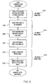
- This embodiment of the patterned beam scan comprises an n x n square array of such centers of the beam intensity distribution with n being odd and equal to or greater than 3, see for example, the pattern 192 of Fig. 6 which forms a 5 x 5 square array.
- the particular physical dimensions of the pattern are a function of the image magnification provided by the energy filtering system 120 and the size of the active area of the electron camera.
- the magnification is approximately 20 and the active area of the electron camera is 25 mm x 25 mm, thus the patterned beam scan, defining pattern 192, irrespective of geometry, must have an overall size of about 1 mm x 1 mm.
- the computer 126 captures the image of the patterned beam scan, defining pattern 192 with the electron camera and determines the location of each center of the beam intensity distribution within the image. The displacement of the location of each center of the beam intensity distribution of the pattern image from its anticipated position with perfectly adjusted optics, is measured, processed and converted by the computer 126 into correcting adjustments to currents Im1, Im2 and Ich passing through the aforementioned quadrupole lenses.
- the computer 126 follows the procedure diagrammed in Fig. 7 .
- the slit assembly 128 is retracted from the beam path and the pattern is inserted into the beam path, see block 194.
- the imaged pattern beam intensity distribution is then measured and stored by the computer 126 for later retrieval, see blocks 196, 198.
- +Measurement of the imaged pattern beam intensity distribution positions is repeated and, for each center of the beam intensity, the difference between its current position and that measured before the change in beam energy is determined, see blocks 202, 204.
- the resulting differences for all centers of the beam intensity are averaged and the net average displacement, Dc, is taken as a measure of the system's departure from a true achromatic imaging condition.
- the present value of Dc is substituted for dDc on the left side of equation (2), the equation is solved for dlch and the current passing through the chromatic adjustment quadrupole lens is reduced by dIch, see block 222. If greater focus precision is required, the procedure may be iterated starting with a new measurement of the imaged beam intensity distribution positions and calculation of Dc. Iteration is performed until Dc is substantially zero, i.e., within an operator specified tolerance. The image 138 formed at the beam detector assembly 130 is then deemed to be achromatic.
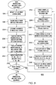
- the computer 126 follows the procedure diagrammed in Fig. 8 .
- the imaged centers of the beam intensity distribution positions of the patterned beam scan, defining pattern 192 are once again measured, see block 224.
- the average distance between the top row of centers of the beam intensity 192A and the bottom row of centers of the beam intensity 192B is calculated as a fraction of the vertical dimension of the active area of the electron camera, see block 226. This fraction is taken as a measure of the magnification in the vertical dimension.
- the horizontal magnification is measured in an analogous fashion using the left-most and right-most columns of centers of the beam intensity 192C,192D, see block 228.
- the average of the vertical and horizontal magnifications is then calculated and stored for later retrieval by the computer 126 to obtain the overall magnification, M, of the image 138, as is the ratio of the vertical to the horizontal magnification which is utilized to obtain the aspect ratio, A, of the image 138, see block 230. If M or A is outside of operator specified tolerances, see block 232, the current, Im1, passing through the one of the aforementioned quadrupole lenses of the post-slit optics 136 is then changed and the measurement of magnification, M, and aspect ratio A is repeated, see blocks 234, 236.
- Im1 is then restored to its original value and the current Im2, passing through the other relevant quadrupole lens, is changed, see block 240.
- dM dM / lm ⁇ 1 ⁇ dlm ⁇ 1 + dM / dlm ⁇ 2 ⁇ dlm ⁇ 2
- dA dA / lm ⁇ 1 ⁇ dlm ⁇ 1 + dA / dlm ⁇ 2 ⁇ dlm ⁇ 2
- the current changes thus determined are applied to the corresponding quadrupole lenses, see block 248.
- the measurements of M and A are repeated and, if the measured values still deviate from their preferred values by more than operator specified tolerances, the entire procedure, starting with the controlled changes to Im1 and Im2, is iterated until the specified tolerances are met.
- the focus of the energy loss spectrum at the slit assembly 128 is assessed through use of the upper knife edge 128U of the energy-selecting slit assembly 128. Focus assessment is based on the variation of the beam intensity across the image 138 at the electron camera as beam energy is varied by means of the accelerating voltage at the electron gun 102 to scan the zero-loss peak of the energy loss spectrum across the knife edge 128U.
- the image intensity across the entire detector area of the electron camera will abruptly go from zero intensity to full intensity as the zero loss peak is scanned across the knife edge 128U from a fully obscured to an unobscured position, or from full intensity to zero intensity as the zero loss peak is scanned across the knife edge 128U from an unobscured position to a fully obscured position.
- a defect of 1st-order focus along the energy dimension of the spectrum will cause beam intensity to first appear at the top or bottom edge of the image 138 at the electron camera and then gradually across the entire detector area of the camera as the defocused zero-loss peak is directed fully past the knife edge 128U.
- a defect of focus orthogonal to the energy dimension of the spectrum gives rise to a gradual disclosure of beam intensity from the left or right edge of the image 138 at the electron camera.
- the rate and orientation of beam intensity disclosure at the image 138 are measured, processed and converted by the computer 126 into correcting adjustments to currents Ifx and Ify passing through the spectrum-focusing quadrupole lenses that are part of the pre-slit optics 122.
- the computer 126 follows the procedure diagrammed in Fig. 9 .
- the entrance aperture assembly 118 is retracted from the electron beam path, the slit assembly 128 is inserted into the beam path by the computer 126, and the upper slit half U is moved downward by an amount SO/2 which is equal to one half the original slit opening 128S, see block 250.
- the beam energy is then changed by the computer 126 via the accelerating voltage at the electron gun 102 to move the zero loss peak of the spectrum up by an amount SO/4, i.e., one half the current slit opening above the upper knife edge 128U of the upper slit half U, see block 252.
- the electron camera is then controlled via the computer 126 to begin integrating beam intensity impinging at the image 138 while scanning the electron beam in energy across the upper knife edge 128U of the upper slit half U of the slit opening 128S, i.e., continuously and at a constant rate changing the beam energy to gradually shift the zero loss peak to a position SO/4 below the upper knife edge 128U, see block 254.
- the position SO/4 below the upper knife edge 128U is not critical but is used to ensure that the electron beam is not scanned onto the lower slit half L of the slit opening 128S.
- the electron camera Upon completion of the beam energy scan, the electron camera is controlled to halt integration of image intensity and to read out and transfer acquired image data to the computer 126.
- a surface plot of image intensity versus horizontal and vertical position within the image represents a surface that is tilted to the degree and direction that the spectrum is defocused, see block 256. In other words, if the spectrum is perfectly focused, the surface plot, termed the isochromatic surface, will be a perfectly flat and horizontal plane.
- F1 and F2 1st order aberration coefficients, give the slope of the isochromatic surface in the two orthogonal directions and serve as direct measures of the degree of spectrum defocus. If F1 or F2 is outside of specified tolerances, see block 258, the currents Ifx and Ify passing through spectrum-focusing quadrupole lenses that are part of the pre-slit optics 122 are changed by the computer 126 and the measurement of the coefficients F1 and F2 is repeated, see blocks 260-264.
- the current value of F1 is substituted for dF1 on the left side of equation (12) and the current value of F2 is substituted for dF2 on the left side of equation (13).
- the computer 126 solves each of the resulting equations for dIfx and dIfy and applies the current changes to the spectrum-focusing quadrupole lenses, see block 270.
- the energy loss spectrum is then deemed to be focused to correct the 1 st order aberration defects of the electron optics of the energy filtering system 120. If greater focus precision is required to attain operator specified tolerances, the procedure may be iterated starting with a new measurement of the isochromatic surface and calculation of new coefficients F1 and F2.
- the computer 126 restores the slit opening 128S to its original size and recenters the zero loss peak of the energy loss spectrum within the slit opening 128S.
- correction of the 2nd order aberration defects of the electron optics of the energy filtering system 120 are next performed, see 274 in Fig. 3 .
- the two most noticeable 2nd order aberration defects of the electron optics of the energy filtering system 120 are exhibited as geometric distortions of the image 138 formed at the beam detector assembly 130 which can not be accounted for simply in terms of a non-unity aspect ratio, see block 276 in Fig. 3 ; and, additional defects of the focus of the energy loss spectrum at the energy-selecting slit assembly 128 resulting not from tilts of the isochromatic surface but rather from curvature of the isochromatic surface, see block 278 in Fig. 3 .
- the 2nd order defects are corrected by the computer 126 following the procedures diagrammed in Figs. 10 and 11 which are extensions of the methods used to measure the corresponding 1 st order defects.
- the distortions in image 138 are corrected by varying currents, Id1, Id2, and Id3, passing through three distortion correcting sextupole lenses that are part of the post-slit optics 136.
- the 2nd order focus of the energy loss spectrum at the energy-selecting slit assembly 128 is adjusted by varying currents, Isx and Isy, passing through two orthogonal sextupole lenses that are part of the pre-slit optics 122.
- the computer 126 captures the image of the patterned beam scan, defining pattern 192, with the electron camera and determines the location of each center of the beam intensity distribution within the image, see blocks 280, 282.
- the following general equations for measured center of the beam intensity position (Xm, Ym) versus nominal center of the beam intensity position (x,y) are used as models in a pair of two dimensional least squares fits, one for horizontal measured coordinates, Xm, and the other for vertical measured coordinates, Ym.
- the nominal center of the beam intensity coordinates, x and y each range over the following set of values: ⁇ -1.0, -0.5, 0.0, 0.5, 1.0 ⁇ .
- the primary goal of this aspect of the present invention is therefore the nullification of the three aberration coefficients CX20, CX02, and CY11 through adjustments to the currents Id1, Id2, and Id3 passing through the aforementioned three sextupole lenses of the post-slit optics 136, see blocks 286, 288.
- the computer 126 first assesses, in turn, the effects of changes to each of the sextupole lens currents, Id1, Id2, and Id3.
- the computer 126 then calculates values for dCX20/dId2, dCX02/dId2, and dCY11/dId2.
- the computer 126 resets the value of Id2 to its original value, changes the current Id3, and calculates values for dCX20/dId3, dCX02/dId3, and dCY11/dId3, see blocks 296, 298.
- the computer 126 substitutes the current value of each of the coefficients, CX20, CX02, and CY11, on the left side of the corresponding equation of the equations (19), (20) and (21).
- the resulting system of three linear equations is solved for dId1, dld2, and dld3 and the resulting current changes are applied to the corresponding sextupole lenses, see block 300.
- the measurement of CX20, CX02, and CY11 is then repeated. If the coefficient magnitudes are still greater than operator specified tolerances, then the entire procedure, starting with the controlled changes to Id1 through Id3, is iterated until the specified tolerances are met.
- the adjustment of spectrum focus to correct 2nd order aberrations begins with the isochromatic surface data collected for the corrections of 1st order aberrations in the energy loss spectrum focus.
- S2, and S3 are the 2nd order aberration coefficients that quantitatively express the defect of 2nd order spectrum focus, i.e., if the spectrum is exactly in focus relative to 2nd order aberrations then each of S1, S2, and S3 has vanishing magnitude, see block 302. If (S1-S2) or S3 is too large, see block 304, the computer 126 then proceeds to change the currents, Isx and Isy, passing through the spectrum focusing sextupole lenses that are part of the pre-slit optics 122 and repeats the measurement of the aberration coefficients S1, S2, and S3, see blocks 306-310.
- the arrangement of the sextupole lenses is such that changes in Isx alter S1 and S2 by equal amounts but in opposite directions, while changes in Isy alter S3 exclusively.
- Optimal focus is thus achieved by nullifying the difference between the first two coefficients, S1, S2, and independently nullifying S3.
- the computer 126 substitutes current values of (S1-S2) and S3 on the left sides of equations (25) and (26), respectively, and solves for the required sextupole lens current changes dIsx and dIsy.
- the currents Isx and Isy are reduced by the determined current changes and the energy loss spectrum is thereby deemed to be focused to the 2nd order, see block 316. If greater focus precision is required, the procedure may be iterated starting with a new measurement of the isochromatic surface and calculation of new (S1-S2) and S3.
- the automatic adjustment of the electron optical elements is made possible by a link between the computer 126 and the energy filtering system 120, which permits the computer 126 to adjust the filter's electron optical elements under software control.
- the preferred link between the computer 126 and the energy filtering system 120 is a digital one, as illustrated through the EFTEM controller 112, but it is also possible to control the required electron optical elements by producing controlling voltages using digital-to-analog (D/A) converters driven by the computer 126, and sending appropriate voltages to analog summing junctions of the electronics of the energy filtering system 120.
- D/A digital-to-analog
- the beam at the entrance to the energy filtering system 120 is spread out but imprinted with a well-defined intensity distribution, such as normally occurs due to passage of the beam through the sample 110.
- the beam is scanned or deflected at the entrance to the energy filtering system 120 such that the center of the beam intensity distribution is successively placed at discrete positions corresponding to patterns of any appropriate known geometry and dimension selected for use in the invention.
- the scanned beam is imaged on the beam detector assembly 130, just as with the focused beam approach described immediately above.
- the resulting scanned spread beam images are cross-correlated with yet another electron beam image taken without scanning or deflecting the beam, i.e., an undeflected beam image.
- Each cross correlation yields an image containing a peak marking the effective displacement of each scan position due to the aberrations/distortions of the energy filter.
- These cross-correlation peak images are superimposed to yield spot pattern images equivalent to those obtained in the preceding focused beam approach and all the analyses and adjustments described above may be performed exactly as before.
- any modem transmission electron microscope provides several lenses that can serve to finely focus the beam at the entrance to the energy filtering system 120.
- the electron microscope also provides several sets of deflector elements that may be used to perform the patterned beam scan. These include the coils of the illumination deflector system 106 used to scan the illumination incident on the specimen, the image shift coils 115 used to align the initial specimen image with the optic axis of the projector lens system, or any projection system alignment coils 117 that precede the energy filtering system 120.
- the invention is generally applicable to energy filtering systems associated with any form of electron microscope, for example scanning transmission electron microscopes.
- the invention is generally applicable to EFTEMs wherever the energy filtering system may be located within the microscope.
- the invention is described with reference to a post-column EFTEM, it is equally applicable to in-column EFTEMs.
- currents were adjusted within the electron lenses of the EFTEM for the described embodiment, the invention is equally applicable to control of the electron lenses by forward or backward movement of the lenses along the optic axis of the microscope.
- the invention of the present application has been described relative to pre-slit and post-slit electron optics which, as described, is the currently preferred form of the invention.
- the only stipulation as to the positioning of the electron optics is that the optic elements which are used to adjust the spectrum at the slit plane must be pre-slit elements.
- the remaining optic elements may be positioned virtually anywhere between the entrance to the energy filtering system 120, even before the entrance aperture assembly 118, and the final image.
- the essential requirement in each instance is that the electron optic elements be so disposed and have sufficient strength to affect and correct the aberrations.
- the currently preferred control of the beam energy in order to characterize energy-depend aberrations is to vary the accelerating voltage at the TEM electron gun 102
- an offset voltage can be applied to an evacuated metal tube or drift tube of the energy filtering system 120 to effectively temporarily change the electron energies while they are in the electromagnetic field of the electron prism.
- the electron prism current can be varied.
- the computer 126 used to receive and analyze images can be replaced by a distributed computing system in which a first part receives images from the beam detector assembly 130; a second part, such as an array processor or other dedicated image processing hardware, performs fast computation of the noted parameters; and, either the first or the second part, or yet another part, determines the needed adjustments and communicates them to the microscope electronics.
- a distributed computing system in which a first part receives images from the beam detector assembly 130; a second part, such as an array processor or other dedicated image processing hardware, performs fast computation of the noted parameters; and, either the first or the second part, or yet another part, determines the needed adjustments and communicates them to the microscope electronics.
Landscapes
- Chemical & Material Sciences (AREA)
- Analytical Chemistry (AREA)
- Electron Sources, Ion Sources (AREA)
Applications Claiming Priority (3)
| Application Number | Priority Date | Filing Date | Title |
|---|---|---|---|
| US138416 | 1980-04-08 | ||
| US09/138,416 US6184524B1 (en) | 1996-08-07 | 1998-08-24 | Automated set up of an energy filtering transmission electron microscope |
| PCT/US1999/018186 WO2000011702A1 (en) | 1998-08-24 | 1999-08-11 | Automated set up of an energy filtering transmission electron microscope |
Publications (2)
| Publication Number | Publication Date |
|---|---|
| EP1110232A1 EP1110232A1 (en) | 2001-06-27 |
| EP1110232B1 true EP1110232B1 (en) | 2009-11-25 |
Family
ID=22481908
Family Applications (1)
| Application Number | Title | Priority Date | Filing Date |
|---|---|---|---|
| EP99967841A Expired - Lifetime EP1110232B1 (en) | 1998-08-24 | 1999-08-11 | Automated set up of an energy filtering transmission electron microscope |
Country Status (5)
| Country | Link |
|---|---|
| US (1) | US6184524B1 (enExample) |
| EP (1) | EP1110232B1 (enExample) |
| JP (1) | JP2002523869A (enExample) |
| DE (1) | DE69941711D1 (enExample) |
| WO (1) | WO2000011702A1 (enExample) |
Cited By (2)
| Publication number | Priority date | Publication date | Assignee | Title |
|---|---|---|---|---|
| EP4386809A1 (en) * | 2022-12-14 | 2024-06-19 | Gatan Inc. | System and method of operating an electron energy loss spectrometer |
| EP4625468A3 (en) * | 2024-03-29 | 2025-10-22 | FEI Company | Automatic correction of energy dependent defocus in particle beam systems due to a configuration change |
Families Citing this family (18)
| Publication number | Priority date | Publication date | Assignee | Title |
|---|---|---|---|---|
| NL1009959C2 (nl) * | 1998-08-28 | 2000-02-29 | Univ Delft Tech | Elektronenmicroscoop. |
| JP3687541B2 (ja) * | 1999-01-04 | 2005-08-24 | 株式会社日立製作所 | 元素マッピング装置、走査透過型電子顕微鏡および元素マッピング方法 |
| EP1209720A3 (en) * | 2000-11-21 | 2006-11-15 | Hitachi High-Technologies Corporation | Energy spectrum measurement |
| US20020170887A1 (en) * | 2001-03-01 | 2002-11-21 | Konica Corporation | Optical element producing method, base material drawing method and base material drawing apparatus |
| US6878935B2 (en) * | 2002-04-03 | 2005-04-12 | General Phosphorix | Method of measuring sizes in scan microscopes |
| GB2393571B (en) * | 2002-09-26 | 2007-03-21 | Leo Electron Microscopy Ltd | Improvements in and relating to the control of instruments |
| JP2004288519A (ja) * | 2003-03-24 | 2004-10-14 | Hitachi High-Technologies Corp | 電子顕微鏡 |
| DE102005014794B4 (de) * | 2005-03-31 | 2009-01-15 | Advanced Micro Devices, Inc., Sunnyvale | Verfahren zum Prüfen einer Halbleiterprobe mit mehreren Abtastungen |
| JP4464857B2 (ja) * | 2005-04-05 | 2010-05-19 | 株式会社日立ハイテクノロジーズ | 荷電粒子線装置 |
| NL1029129C2 (nl) * | 2005-05-25 | 2006-11-28 | Univ Delft Tech | Scanningtransmissie-elektronenmicroscoop. |
| US7238938B2 (en) * | 2005-06-16 | 2007-07-03 | Gatan, Inc. | Energy selecting slit and energy selective sample analysis systems utilizing the same |
| JP5315033B2 (ja) * | 2008-12-09 | 2013-10-16 | 株式会社日立ハイテクノロジーズ | 電子分光器を備えた透過型電子顕微鏡 |
| US8373137B2 (en) * | 2010-09-24 | 2013-02-12 | Nion Co. | High resolution energy-selecting electron beam apparatus |
| JP6340216B2 (ja) * | 2014-03-07 | 2018-06-06 | 株式会社日立ハイテクノロジーズ | 走査電子顕微鏡 |
| CN106804114B (zh) * | 2014-06-27 | 2019-05-28 | 加坦公司 | 电子能量损失光谱仪 |
| EP2998979A1 (en) * | 2014-09-22 | 2016-03-23 | Fei Company | Improved spectroscopy in a transmission charged-particle microscope |
| JP2017143060A (ja) | 2016-01-20 | 2017-08-17 | ガタン インコーポレイテッドGatan,Inc. | 直接検出センサを用いる電子エネルギー損失分光器 |
| EP4002420A1 (en) | 2020-11-12 | 2022-05-25 | FEI Company | Method of determining an energy width of a charged particle beam |
Family Cites Families (59)
| Publication number | Priority date | Publication date | Assignee | Title |
|---|---|---|---|---|
| NL6716628A (enExample) | 1967-12-07 | 1969-06-10 | ||
| NL7012388A (enExample) | 1970-08-21 | 1972-02-23 | ||
| US4017403A (en) | 1974-07-31 | 1977-04-12 | United Kingdom Atomic Energy Authority | Ion beam separators |
| SU516316A1 (ru) | 1975-03-03 | 1976-11-25 | Ордена Ленина Физико-Технический Институт Им. А.Ф.Иоффе | Электроннооптическое устройство со скорректированной сферической аберрацией |
| GB2002547B (en) | 1977-07-30 | 1982-01-20 | Tee W | Investigation of astigmatism in electron beam probe instruments |
| US4379250A (en) | 1979-10-19 | 1983-04-05 | Hitachi, Ltd. | Field emission cathode and method of fabricating the same |
| JPS5848011B2 (ja) | 1979-11-26 | 1983-10-26 | 日本鋼管株式会社 | 加熱炉燃焼制御方法 |
| SU920892A1 (ru) | 1980-07-23 | 1982-04-15 | Ордена Ленина физико-технический институт им.А.Ф.Иоффе | Электроннооптическое устройство со скорректированной сферической аберрацией |
| NL8100142A (nl) | 1981-01-14 | 1982-08-02 | Philips Nv | Inrichting voor het weergeven van beelden met behulp van een kathodestraalbuis. |
| NL8101888A (nl) | 1981-04-16 | 1982-11-16 | Philips Nv | Beeldweergeefinrichting. |
| GB2109539A (en) | 1981-11-02 | 1983-06-02 | Philips Electronic Associated | Electron beam alignment |
| GB2109538A (en) | 1981-11-02 | 1983-06-02 | Philips Electronic Associated | Electron beam alignment |
| US4414474A (en) | 1982-02-17 | 1983-11-08 | University Patents, Inc. | Corrector for axial aberrations in electron optic instruments |
| SU1048532A1 (ru) | 1982-05-14 | 1983-10-15 | Предприятие П/Я М-5273 | Электроннооптическое устройство с коррекцией аберраций |
| GB8322017D0 (en) | 1983-08-16 | 1983-09-21 | Vg Instr Ltd | Charged particle energy spectrometer |
| DE3423149A1 (de) | 1984-06-22 | 1986-01-02 | Fa. Carl Zeiss, 7920 Heidenheim | Verfahren und anordnung zur elektronenenergiegefilterten abbildung eines objektes oder eines objektbeugungsdiagrammes mit einem transmissions-elektronenmikroskop |
| JPS61277141A (ja) | 1985-05-31 | 1986-12-08 | Jeol Ltd | 磁界型エネルギ−フイルタ− |
| DE3532698A1 (de) | 1985-09-13 | 1987-03-26 | Zeiss Carl Fa | Elektronenenergiefilter vom alpha-typ |
| DE3532699A1 (de) | 1985-09-13 | 1987-03-26 | Zeiss Carl Fa | Elektronenenergiefilter vom omega-typ |
| JPS6298724A (ja) | 1985-10-25 | 1987-05-08 | Hitachi Ltd | 電子線描画装置 |
| NL8600685A (nl) | 1986-03-18 | 1987-10-16 | Philips Nv | Apparaat voor energie selectieve afbeelding. |
| JPS62240442A (ja) | 1986-04-09 | 1987-10-21 | Hitachi Ltd | 燃料制御装置 |
| NL8602177A (nl) | 1986-08-27 | 1988-03-16 | Philips Nv | Electronen detectie met energie discriminatie. |
| US4743756A (en) | 1987-08-10 | 1988-05-10 | Gatan Inc. | Parallel-detection electron energy-loss spectrometer |
| US4851670A (en) | 1987-08-28 | 1989-07-25 | Gatan Inc. | Energy-selected electron imaging filter |
| NL8702400A (nl) | 1987-10-09 | 1989-05-01 | Philips Nv | Kleurenbeeldbuis met asymmetrische deflektie-elektroden. |
| JPH01107532A (ja) | 1987-10-21 | 1989-04-25 | Hitachi Ltd | 電子線描画装置 |
| NL8702700A (nl) | 1987-11-12 | 1989-06-01 | Philips Nv | Werkwijze en inrichting voor automatische fasecorrectie van complexe nmr spectra. |
| NL8801050A (nl) | 1988-04-22 | 1989-11-16 | Philips Nv | Beeldversterkerbuis. |
| JP2686492B2 (ja) | 1988-12-12 | 1997-12-08 | 株式会社日立製作所 | 透過形電子顕微鏡の照射位置決め方法 |
| JP2842879B2 (ja) | 1989-01-06 | 1999-01-06 | 株式会社日立製作所 | 表面分析方法および装置 |
| NL8900067A (nl) | 1989-01-12 | 1990-08-01 | Philips Nv | Beeldweergeefinrichting. |
| US5343112A (en) | 1989-01-18 | 1994-08-30 | Balzers Aktiengesellschaft | Cathode arrangement |
| FR2642243B1 (fr) | 1989-01-24 | 1991-04-19 | Labo Electronique Physique | Circuit de predistorsion adaptative |
| GB2233124B (en) | 1989-06-06 | 1994-02-09 | Mitsubishi Electric Corp | Ion implantation apparatus |
| JP2791103B2 (ja) | 1989-06-09 | 1998-08-27 | 株式会社日立製作所 | 表面計測方法および装置 |
| US5004919A (en) | 1989-07-05 | 1991-04-02 | Jeol, Ltd. | Transmission electron microscope |
| US5225999A (en) | 1990-07-06 | 1993-07-06 | The Trustees Of The University Of Pennsylvania | Magnetic environment stabilization for effective operation of magnetically sensitive instruments |
| DE69030996T2 (de) | 1990-08-09 | 1998-01-02 | Philips Electronics Nv | Elektronenstrahlvorrichtung mit monopolförmigem, magnetischem Feld |
| NL9100380A (nl) | 1991-03-01 | 1992-10-01 | Philips Nv | Kathodestraalbuis met elektronenkanon met planparallelle optiek. |
| US5177631A (en) | 1991-06-28 | 1993-01-05 | Eastman Kodak Company | Magnetic position sensor |
| DE69213157T2 (de) | 1991-10-24 | 1997-03-06 | Philips Electronics Nv | Elektronenstrahlvorrichtung |
| DE69322890T2 (de) | 1992-02-12 | 1999-07-29 | Koninklijke Philips Electronics N.V., Eindhoven | Verfahren zur Verringerung einer räumlichen energiedispersiven Streuung eines Elektronenstrahlenbündels und eine für den Einsatz eines solchen Verfahrens geeignete Elektronenstrahlvorrichtung |
| DE69316960T2 (de) | 1992-11-12 | 1998-07-30 | Koninkl Philips Electronics Nv | Elektronenröhre mit Halbleiterkathode |
| US5432347A (en) | 1992-11-12 | 1995-07-11 | U.S. Philips Corporation | Method for image reconstruction in a high-resolution electron microscope, and electron microscope suitable for use of such a method |
| US5393976A (en) | 1992-11-26 | 1995-02-28 | Kabushiki Kaisha Topcon | Apparatus for displaying a sample image |
| JP3397347B2 (ja) | 1992-11-26 | 2003-04-14 | 日本電子株式会社 | オメガフィルタ |
| DE4310559A1 (de) | 1993-03-26 | 1994-09-29 | Zeiss Carl Fa | Abbildendes Elektronenenergiefilter |
| DE69402283T2 (de) | 1993-05-21 | 1997-09-18 | Philips Electronics Nv | Energiefilter mit Korrektur von chromatischen Aberrationen zweiter ordnung |
| JPH0712755A (ja) * | 1993-06-23 | 1995-01-17 | Res Dev Corp Of Japan | 電子線装置の調整方法および装置 |
| US5414261A (en) | 1993-07-01 | 1995-05-09 | The Regents Of The University Of California | Enhanced imaging mode for transmission electron microscopy |
| DE4328649A1 (de) | 1993-08-26 | 1995-03-02 | Zeiss Carl Fa | Elektronenoptisches Abbildungssystem mit regelbaren Elementen |
| US5578823A (en) | 1994-12-16 | 1996-11-26 | Hitachi, Ltd. | Transmission electron microscope and method of observing element distribution by using the same |
| JPH08195298A (ja) | 1995-01-13 | 1996-07-30 | Nissin High Voltage Co Ltd | ビームエネルギー安定化装置 |
| US5640012A (en) | 1995-08-25 | 1997-06-17 | Gatan, Inc. | Precision-controlled slit mechanism for electron microscope |
| US5798524A (en) | 1996-08-07 | 1998-08-25 | Gatan, Inc. | Automated adjustment of an energy filtering transmission electron microscope |
| JP3490597B2 (ja) * | 1997-01-07 | 2004-01-26 | 株式会社東芝 | マスク検査装置 |
| JP3439614B2 (ja) * | 1997-03-03 | 2003-08-25 | 株式会社日立製作所 | 透過型電子顕微鏡及び元素分布観察方法 |
| JPH10284384A (ja) * | 1997-04-09 | 1998-10-23 | Fujitsu Ltd | 荷電粒子ビーム露光方法及び装置 |
-
1998
- 1998-08-24 US US09/138,416 patent/US6184524B1/en not_active Expired - Lifetime
-
1999
- 1999-08-11 WO PCT/US1999/018186 patent/WO2000011702A1/en not_active Ceased
- 1999-08-11 DE DE69941711T patent/DE69941711D1/de not_active Expired - Lifetime
- 1999-08-11 EP EP99967841A patent/EP1110232B1/en not_active Expired - Lifetime
- 1999-08-11 JP JP2000566874A patent/JP2002523869A/ja active Pending
Cited By (2)
| Publication number | Priority date | Publication date | Assignee | Title |
|---|---|---|---|---|
| EP4386809A1 (en) * | 2022-12-14 | 2024-06-19 | Gatan Inc. | System and method of operating an electron energy loss spectrometer |
| EP4625468A3 (en) * | 2024-03-29 | 2025-10-22 | FEI Company | Automatic correction of energy dependent defocus in particle beam systems due to a configuration change |
Also Published As
| Publication number | Publication date |
|---|---|
| EP1110232A1 (en) | 2001-06-27 |
| WO2000011702A1 (en) | 2000-03-02 |
| JP2002523869A (ja) | 2002-07-30 |
| DE69941711D1 (de) | 2010-01-07 |
| US6184524B1 (en) | 2001-02-06 |
Similar Documents
| Publication | Publication Date | Title |
|---|---|---|
| EP0917725B1 (en) | Automated adjustment of an energy filtering transmissiion electron microscope | |
| EP1110232B1 (en) | Automated set up of an energy filtering transmission electron microscope | |
| US5750990A (en) | Method for measuring critical dimension of pattern on sample | |
| EP2387062B1 (en) | Simultaneous electron detection | |
| EP1993074B1 (en) | Image evaluation system and charged particle beam microscope | |
| Krivanek et al. | An imaging filter for biological applications | |
| US8008622B2 (en) | Electron beam apparatus and method of generating an electron beam irradiation pattern | |
| KR101829797B1 (ko) | 멀티 하전 입자빔상의 회전각 측정 방법, 멀티 하전 입자빔상의 회전각 조정 방법 및 멀티 하전 입자빔 묘화 장치 | |
| US6765217B1 (en) | Charged-particle-beam mapping projection-optical systems and methods for adjusting same | |
| US20060011836A1 (en) | Element mapping unit, scanning transmission electron microscope, and element mapping method | |
| JPWO2000041206A1 (ja) | 元素マッピング装置、走査透過型電子顕微鏡および元素マッピング方法 | |
| US20200388462A1 (en) | Systems and methods for tuning and calibrating charged particle beam apparatus | |
| US5396077A (en) | Electron beam lithography apparatus having electron optics correction system | |
| US20070085020A1 (en) | Method for controlling charged particle beam, and charged particle beam apparatus | |
| TWI824298B (zh) | 校正歸因於二次射束之反掃描偏轉而散焦的二次射束之焦點的方法及相關電腦可讀媒體 | |
| US10403487B2 (en) | Quantitative measurements of elemental and molecular species using high mass resolution mass spectrometry | |
| EP1105913B1 (en) | Electron microscope | |
| JP4449573B2 (ja) | 元素マッピング装置,走査透過型電子顕微鏡および元素マッピング方法 | |
| Gubbens et al. | A post-column imaging energy filter with a 20482-pixel slow-scan CCD camera | |
| EP4531072A1 (en) | Method of assessing a charged particle beam, and method of assessing a beam grid | |
| US12451325B2 (en) | Charged particle beam axial calibration | |
| EP4575637A1 (en) | Method and apparatus for assessing a sample surface, method of scanning a sample surface, and charged particle assessment apparatus | |
| JP2000100695A (ja) | 荷電ビーム描画装置および方法 | |
| WO2025131457A1 (en) | Method and apparatus for assessing a sample surface, method of scanning a sample surface, and charged particle assessment apparatus | |
| EP1428006B1 (en) | Method and apparatus for scanned instrument calibration |
Legal Events
| Date | Code | Title | Description |
|---|---|---|---|
| PUAI | Public reference made under article 153(3) epc to a published international application that has entered the european phase |
Free format text: ORIGINAL CODE: 0009012 |
|
| 17P | Request for examination filed |
Effective date: 20010323 |
|
| AK | Designated contracting states |
Kind code of ref document: A1 Designated state(s): AT BE CH CY DE DK ES FI FR GB GR IE IT LI LU MC NL PT SE |
|
| RBV | Designated contracting states (corrected) |
Designated state(s): DE FR GB |
|
| 17Q | First examination report despatched |
Effective date: 20040510 |
|
| GRAP | Despatch of communication of intention to grant a patent |
Free format text: ORIGINAL CODE: EPIDOSNIGR1 |
|
| GRAS | Grant fee paid |
Free format text: ORIGINAL CODE: EPIDOSNIGR3 |
|
| GRAA | (expected) grant |
Free format text: ORIGINAL CODE: 0009210 |
|
| AK | Designated contracting states |
Kind code of ref document: B1 Designated state(s): DE FR GB |
|
| REG | Reference to a national code |
Ref country code: GB Ref legal event code: FG4D |
|
| REF | Corresponds to: |
Ref document number: 69941711 Country of ref document: DE Date of ref document: 20100107 Kind code of ref document: P |
|
| PLBE | No opposition filed within time limit |
Free format text: ORIGINAL CODE: 0009261 |
|
| STAA | Information on the status of an ep patent application or granted ep patent |
Free format text: STATUS: NO OPPOSITION FILED WITHIN TIME LIMIT |
|
| 26N | No opposition filed |
Effective date: 20100826 |
|
| REG | Reference to a national code |
Ref country code: FR Ref legal event code: PLFP Year of fee payment: 17 |
|
| REG | Reference to a national code |
Ref country code: FR Ref legal event code: PLFP Year of fee payment: 18 |
|
| REG | Reference to a national code |
Ref country code: FR Ref legal event code: PLFP Year of fee payment: 19 |
|
| REG | Reference to a national code |
Ref country code: FR Ref legal event code: PLFP Year of fee payment: 20 |
|
| PGFP | Annual fee paid to national office [announced via postgrant information from national office to epo] |
Ref country code: DE Payment date: 20180830 Year of fee payment: 20 Ref country code: FR Payment date: 20180830 Year of fee payment: 20 |
|
| PGFP | Annual fee paid to national office [announced via postgrant information from national office to epo] |
Ref country code: GB Payment date: 20180830 Year of fee payment: 20 |
|
| REG | Reference to a national code |
Ref country code: DE Ref legal event code: R071 Ref document number: 69941711 Country of ref document: DE |
|
| REG | Reference to a national code |
Ref country code: GB Ref legal event code: PE20 Expiry date: 20190810 |
|
| PG25 | Lapsed in a contracting state [announced via postgrant information from national office to epo] |
Ref country code: GB Free format text: LAPSE BECAUSE OF EXPIRATION OF PROTECTION Effective date: 20190810 |
|
| P01 | Opt-out of the competence of the unified patent court (upc) registered |
Effective date: 20230615 |