EP1107320A2 - Méthode et appareil pour fabriquer une couche mince, couche mince et cellule solaire - Google Patents
Méthode et appareil pour fabriquer une couche mince, couche mince et cellule solaire Download PDFInfo
- Publication number
- EP1107320A2 EP1107320A2 EP00125676A EP00125676A EP1107320A2 EP 1107320 A2 EP1107320 A2 EP 1107320A2 EP 00125676 A EP00125676 A EP 00125676A EP 00125676 A EP00125676 A EP 00125676A EP 1107320 A2 EP1107320 A2 EP 1107320A2
- Authority
- EP
- European Patent Office
- Prior art keywords
- protrusions
- sheet
- silicon
- base
- melt
- Prior art date
- Legal status (The legal status is an assumption and is not a legal conclusion. Google has not performed a legal analysis and makes no representation as to the accuracy of the status listed.)
- Withdrawn
Links
- 238000004519 manufacturing process Methods 0.000 title claims description 99
- 238000001816 cooling Methods 0.000 claims abstract description 194
- 239000013078 crystal Substances 0.000 claims abstract description 139
- 239000000463 material Substances 0.000 claims abstract description 77
- 238000007598 dipping method Methods 0.000 claims abstract description 27
- 239000004065 semiconductor Substances 0.000 claims abstract description 21
- 239000000289 melt material Substances 0.000 claims abstract description 18
- 239000007769 metal material Substances 0.000 claims abstract description 18
- 230000002093 peripheral effect Effects 0.000 claims abstract description 10
- XUIMIQQOPSSXEZ-UHFFFAOYSA-N Silicon Chemical compound [Si] XUIMIQQOPSSXEZ-UHFFFAOYSA-N 0.000 claims description 299
- 229910052710 silicon Inorganic materials 0.000 claims description 299
- 239000010703 silicon Substances 0.000 claims description 299
- 229910052770 Uranium Inorganic materials 0.000 claims description 34
- 229910052720 vanadium Inorganic materials 0.000 claims description 33
- OKTJSMMVPCPJKN-UHFFFAOYSA-N Carbon Chemical compound [C] OKTJSMMVPCPJKN-UHFFFAOYSA-N 0.000 claims description 32
- HBMJWWWQQXIZIP-UHFFFAOYSA-N silicon carbide Chemical compound [Si+]#[C-] HBMJWWWQQXIZIP-UHFFFAOYSA-N 0.000 claims description 25
- 229910010271 silicon carbide Inorganic materials 0.000 claims description 23
- 229910052799 carbon Inorganic materials 0.000 claims description 19
- 239000000758 substrate Substances 0.000 claims description 13
- 229910052581 Si3N4 Inorganic materials 0.000 claims description 11
- 239000011248 coating agent Substances 0.000 claims description 11
- 238000000576 coating method Methods 0.000 claims description 11
- HQVNEWCFYHHQES-UHFFFAOYSA-N silicon nitride Chemical compound N12[Si]34N5[Si]62N3[Si]51N64 HQVNEWCFYHHQES-UHFFFAOYSA-N 0.000 claims description 11
- PZNSFCLAULLKQX-UHFFFAOYSA-N Boron nitride Chemical compound N#B PZNSFCLAULLKQX-UHFFFAOYSA-N 0.000 claims description 9
- 229910052582 BN Inorganic materials 0.000 claims description 8
- 238000000034 method Methods 0.000 abstract description 48
- 239000002585 base Substances 0.000 description 203
- 239000000155 melt Substances 0.000 description 70
- 239000007789 gas Substances 0.000 description 56
- 239000011295 pitch Substances 0.000 description 43
- KRHYYFGTRYWZRS-UHFFFAOYSA-N Fluorane Chemical compound F KRHYYFGTRYWZRS-UHFFFAOYSA-N 0.000 description 32
- 239000002826 coolant Substances 0.000 description 30
- 239000002210 silicon-based material Substances 0.000 description 20
- IJGRMHOSHXDMSA-UHFFFAOYSA-N Atomic nitrogen Chemical compound N#N IJGRMHOSHXDMSA-UHFFFAOYSA-N 0.000 description 18
- 230000008018 melting Effects 0.000 description 16
- 238000002844 melting Methods 0.000 description 16
- HEMHJVSKTPXQMS-UHFFFAOYSA-M Sodium hydroxide Chemical compound [OH-].[Na+] HEMHJVSKTPXQMS-UHFFFAOYSA-M 0.000 description 15
- 229910002804 graphite Inorganic materials 0.000 description 12
- 239000010439 graphite Substances 0.000 description 12
- 239000010453 quartz Substances 0.000 description 12
- VYPSYNLAJGMNEJ-UHFFFAOYSA-N silicon dioxide Inorganic materials O=[Si]=O VYPSYNLAJGMNEJ-UHFFFAOYSA-N 0.000 description 12
- ZOXJGFHDIHLPTG-UHFFFAOYSA-N Boron Chemical compound [B] ZOXJGFHDIHLPTG-UHFFFAOYSA-N 0.000 description 11
- GRYLNZFGIOXLOG-UHFFFAOYSA-N Nitric acid Chemical compound O[N+]([O-])=O GRYLNZFGIOXLOG-UHFFFAOYSA-N 0.000 description 11
- 229910052796 boron Inorganic materials 0.000 description 11
- 238000005530 etching Methods 0.000 description 11
- 238000005259 measurement Methods 0.000 description 11
- 229910017604 nitric acid Inorganic materials 0.000 description 11
- 230000007423 decrease Effects 0.000 description 10
- 238000007650 screen-printing Methods 0.000 description 10
- 230000015572 biosynthetic process Effects 0.000 description 9
- 229910052734 helium Inorganic materials 0.000 description 9
- 229910052751 metal Inorganic materials 0.000 description 9
- 239000002184 metal Substances 0.000 description 9
- XKRFYHLGVUSROY-UHFFFAOYSA-N Argon Chemical compound [Ar] XKRFYHLGVUSROY-UHFFFAOYSA-N 0.000 description 8
- 239000001307 helium Substances 0.000 description 7
- SWQJXJOGLNCZEY-UHFFFAOYSA-N helium atom Chemical compound [He] SWQJXJOGLNCZEY-UHFFFAOYSA-N 0.000 description 7
- PXHVJJICTQNCMI-UHFFFAOYSA-N Nickel Chemical compound [Ni] PXHVJJICTQNCMI-UHFFFAOYSA-N 0.000 description 6
- 239000003513 alkali Substances 0.000 description 6
- 238000005266 casting Methods 0.000 description 6
- 238000005520 cutting process Methods 0.000 description 6
- 238000009792 diffusion process Methods 0.000 description 6
- 229910001873 dinitrogen Inorganic materials 0.000 description 6
- 239000011261 inert gas Substances 0.000 description 6
- 229910052757 nitrogen Inorganic materials 0.000 description 6
- 229910000679 solder Inorganic materials 0.000 description 6
- 238000011109 contamination Methods 0.000 description 5
- 230000003247 decreasing effect Effects 0.000 description 5
- 238000010586 diagram Methods 0.000 description 5
- 230000006641 stabilisation Effects 0.000 description 5
- 238000011105 stabilization Methods 0.000 description 5
- 235000012431 wafers Nutrition 0.000 description 5
- 229910052786 argon Inorganic materials 0.000 description 4
- 239000002019 doping agent Substances 0.000 description 4
- 239000000203 mixture Substances 0.000 description 4
- 238000000059 patterning Methods 0.000 description 4
- XHXFXVLFKHQFAL-UHFFFAOYSA-N phosphoryl trichloride Chemical compound ClP(Cl)(Cl)=O XHXFXVLFKHQFAL-UHFFFAOYSA-N 0.000 description 4
- 238000005498 polishing Methods 0.000 description 4
- 238000007711 solidification Methods 0.000 description 4
- 230000008023 solidification Effects 0.000 description 4
- GWEVSGVZZGPLCZ-UHFFFAOYSA-N Titan oxide Chemical compound O=[Ti]=O GWEVSGVZZGPLCZ-UHFFFAOYSA-N 0.000 description 3
- 229910045601 alloy Inorganic materials 0.000 description 3
- 239000000956 alloy Substances 0.000 description 3
- 229910052782 aluminium Inorganic materials 0.000 description 3
- XAGFODPZIPBFFR-UHFFFAOYSA-N aluminium Chemical compound [Al] XAGFODPZIPBFFR-UHFFFAOYSA-N 0.000 description 3
- 239000000919 ceramic Substances 0.000 description 3
- 238000007796 conventional method Methods 0.000 description 3
- 230000000694 effects Effects 0.000 description 3
- 238000010438 heat treatment Methods 0.000 description 3
- 238000005286 illumination Methods 0.000 description 3
- 230000001771 impaired effect Effects 0.000 description 3
- 229910052759 nickel Inorganic materials 0.000 description 3
- 229910021420 polycrystalline silicon Inorganic materials 0.000 description 3
- XLYOFNOQVPJJNP-UHFFFAOYSA-N water Substances O XLYOFNOQVPJJNP-UHFFFAOYSA-N 0.000 description 3
- XEEYBQQBJWHFJM-UHFFFAOYSA-N Iron Chemical compound [Fe] XEEYBQQBJWHFJM-UHFFFAOYSA-N 0.000 description 2
- 229910019213 POCl3 Inorganic materials 0.000 description 2
- OAICVXFJPJFONN-UHFFFAOYSA-N Phosphorus Chemical compound [P] OAICVXFJPJFONN-UHFFFAOYSA-N 0.000 description 2
- 239000002253 acid Substances 0.000 description 2
- 230000002411 adverse Effects 0.000 description 2
- 229910052698 phosphorus Inorganic materials 0.000 description 2
- 239000011574 phosphorus Substances 0.000 description 2
- 238000005268 plasma chemical vapour deposition Methods 0.000 description 2
- GYHNNYVSQQEPJS-UHFFFAOYSA-N Gallium Chemical compound [Ga] GYHNNYVSQQEPJS-UHFFFAOYSA-N 0.000 description 1
- 229910004205 SiNX Inorganic materials 0.000 description 1
- ATJFFYVFTNAWJD-UHFFFAOYSA-N Tin Chemical compound [Sn] ATJFFYVFTNAWJD-UHFFFAOYSA-N 0.000 description 1
- HCHKCACWOHOZIP-UHFFFAOYSA-N Zinc Chemical compound [Zn] HCHKCACWOHOZIP-UHFFFAOYSA-N 0.000 description 1
- QCWXUUIWCKQGHC-UHFFFAOYSA-N Zirconium Chemical compound [Zr] QCWXUUIWCKQGHC-UHFFFAOYSA-N 0.000 description 1
- 238000013019 agitation Methods 0.000 description 1
- PNEYBMLMFCGWSK-UHFFFAOYSA-N aluminium oxide Inorganic materials [O-2].[O-2].[O-2].[Al+3].[Al+3] PNEYBMLMFCGWSK-UHFFFAOYSA-N 0.000 description 1
- 229910052787 antimony Inorganic materials 0.000 description 1
- WATWJIUSRGPENY-UHFFFAOYSA-N antimony atom Chemical compound [Sb] WATWJIUSRGPENY-UHFFFAOYSA-N 0.000 description 1
- 229910052785 arsenic Inorganic materials 0.000 description 1
- RQNWIZPPADIBDY-UHFFFAOYSA-N arsenic atom Chemical compound [As] RQNWIZPPADIBDY-UHFFFAOYSA-N 0.000 description 1
- 239000003575 carbonaceous material Substances 0.000 description 1
- 238000006243 chemical reaction Methods 0.000 description 1
- 238000010924 continuous production Methods 0.000 description 1
- 238000002425 crystallisation Methods 0.000 description 1
- 230000008025 crystallization Effects 0.000 description 1
- 230000007547 defect Effects 0.000 description 1
- 238000009826 distribution Methods 0.000 description 1
- 229910052733 gallium Inorganic materials 0.000 description 1
- 229910052732 germanium Inorganic materials 0.000 description 1
- GNPVGFCGXDBREM-UHFFFAOYSA-N germanium atom Chemical compound [Ge] GNPVGFCGXDBREM-UHFFFAOYSA-N 0.000 description 1
- 230000005484 gravity Effects 0.000 description 1
- 239000003779 heat-resistant material Substances 0.000 description 1
- 239000012535 impurity Substances 0.000 description 1
- 229910052738 indium Inorganic materials 0.000 description 1
- APFVFJFRJDLVQX-UHFFFAOYSA-N indium atom Chemical compound [In] APFVFJFRJDLVQX-UHFFFAOYSA-N 0.000 description 1
- 229910052742 iron Inorganic materials 0.000 description 1
- 230000001788 irregular Effects 0.000 description 1
- 230000003647 oxidation Effects 0.000 description 1
- 238000007254 oxidation reaction Methods 0.000 description 1
- RVTZCBVAJQQJTK-UHFFFAOYSA-N oxygen(2-);zirconium(4+) Chemical compound [O-2].[O-2].[Zr+4] RVTZCBVAJQQJTK-UHFFFAOYSA-N 0.000 description 1
- 238000007747 plating Methods 0.000 description 1
- 239000000843 powder Substances 0.000 description 1
- 230000005855 radiation Effects 0.000 description 1
- 230000003014 reinforcing effect Effects 0.000 description 1
- 238000005096 rolling process Methods 0.000 description 1
- 238000006748 scratching Methods 0.000 description 1
- 230000002393 scratching effect Effects 0.000 description 1
- 238000007493 shaping process Methods 0.000 description 1
- 150000003376 silicon Chemical class 0.000 description 1
- 239000011863 silicon-based powder Substances 0.000 description 1
- 239000000126 substance Substances 0.000 description 1
- 229910052718 tin Inorganic materials 0.000 description 1
- OGIDPMRJRNCKJF-UHFFFAOYSA-N titanium oxide Inorganic materials [Ti]=O OGIDPMRJRNCKJF-UHFFFAOYSA-N 0.000 description 1
- WFKWXMTUELFFGS-UHFFFAOYSA-N tungsten Chemical compound [W] WFKWXMTUELFFGS-UHFFFAOYSA-N 0.000 description 1
- 229910052721 tungsten Inorganic materials 0.000 description 1
- 239000010937 tungsten Substances 0.000 description 1
- 238000007740 vapor deposition Methods 0.000 description 1
- 229910052725 zinc Inorganic materials 0.000 description 1
- 239000011701 zinc Substances 0.000 description 1
- 229910001928 zirconium oxide Inorganic materials 0.000 description 1
Images


Classifications
-
- H—ELECTRICITY
- H01—ELECTRIC ELEMENTS
- H01L—SEMICONDUCTOR DEVICES NOT COVERED BY CLASS H10
- H01L31/00—Semiconductor devices sensitive to infrared radiation, light, electromagnetic radiation of shorter wavelength or corpuscular radiation and specially adapted either for the conversion of the energy of such radiation into electrical energy or for the control of electrical energy by such radiation; Processes or apparatus specially adapted for the manufacture or treatment thereof or of parts thereof; Details thereof
- H01L31/02—Details
- H01L31/0236—Special surface textures
- H01L31/02363—Special surface textures of the semiconductor body itself, e.g. textured active layers
-
- Y—GENERAL TAGGING OF NEW TECHNOLOGICAL DEVELOPMENTS; GENERAL TAGGING OF CROSS-SECTIONAL TECHNOLOGIES SPANNING OVER SEVERAL SECTIONS OF THE IPC; TECHNICAL SUBJECTS COVERED BY FORMER USPC CROSS-REFERENCE ART COLLECTIONS [XRACs] AND DIGESTS
- Y02—TECHNOLOGIES OR APPLICATIONS FOR MITIGATION OR ADAPTATION AGAINST CLIMATE CHANGE
- Y02E—REDUCTION OF GREENHOUSE GAS [GHG] EMISSIONS, RELATED TO ENERGY GENERATION, TRANSMISSION OR DISTRIBUTION
- Y02E10/00—Energy generation through renewable energy sources
- Y02E10/50—Photovoltaic [PV] energy
Definitions
- the present invention relates to a sheet manufacturing method and a manufacturing apparatus of manufacturing a sheet (a plate-like base) from a melt containing a metal material or a semiconductor material.
- the present invention relates to a technique for inexpensively manufacturing solar cells, where a silicon sheet for a solar cell is directly manufactured from a silicon melt.
- the present invention relates to a silicon sheet manufacturing apparatus and method enabling manufacture of a silicon sheet, which has protrusions or curved portions at least on the melt side when viewed in section.
- Examples of conventional methods of manufacturing polycrystalline silicon wafers for use in solar cells include a method of casting to form a polycrystalline body of e.g., silicon, disclosed in Japanese Patent Laying-Open No. 6-64913.
- a high-purity silicon material containing a dopant of phosphorus, boron, or the like is heated to melt in a crucible placed in an inert ambience.
- a silicon melt is poured into a casting mold for gradually cooling, so as to provide a polycrystalline ingot.
- the ingot is to be sliced by a wire saw or inner diameter blade.
- a method of continuously casting a silicon plate involves manufacture of a silicon sheet without slicing.
- a silicon melt is poured into a horizontal heat casting mold and a dummy graphite plate is horizontally inserted such that its leading end is dipped into the silicon melt under a control plate.
- the silicon plate is horizontally pulled out with use of a roller.
- Coolant gas supplied from gas blow-off pipe of a cooling apparatus provides for continuous formation of the silicon plate.
- the manufacturing apparatus for a silicon ribbon generally has a portion of heating to melt silicon and a cooling roller of a heat-resistant material.
- the cooling roller with one end of carbon net wound thereon, is directly dipped into a silicon melt for forming a silicon ribbon on the surface of the cooling roller.
- the carbon net wound on the cooling roller is pulled with rotation of the cooling roller for rolling out thus formed silicon ribbon.
- the manufacturing apparatus allows the silicon ribbon, formed from the silicon that first adhered to the carbon net, to be continuously rolled out.
- the method of continuously casting the silicon plate disclosed in the aforementioned laid-open application No. 7-256624 controls the thickness of the silicon plate by pulling out the silicon plate under the thickness control plate. In this case, it is difficult to control a thickness of 600 ⁇ m or smaller as is employed for solar cells.
- the silicon ribbon formed from the silicon that first adhered to the carbon net is continuously pulled and rolled out with rotation of the cooling roller.
- the silicon ribbon is somewhat fragile due to reaction of the carbon net and the silicon. If the formed silicon is extremely thin, the silicon ribbon may break to fall during pulling operation. In this situation, the operation must be stopped and productivity decreases.
- a mechanism which pressurizes to apply the silicon melt onto the peripheral surface of the cooling roller by jet pressure. Since the pressure is exerted by agitation of the silicon melt, unwanted pressure may be exerted to the formed silicon, thereby causing defects.
- a growth rate of silicon is determined by a number of factors including a temperature of a heater for maintaining the silicon in a molten state, dipping depth, type and flow rate of coolant gas circulating in the cooling roller, rotation speed of the cooling roller and the like. Thus, it is technically difficult to stably pull out the silicon ribbon while controlling the growth rate.
- a wedge is provided for removing any silicon residue left on the surface of the cooling roller. Such a wedge is brought into direct contact with the surface of the cooling roller where silicon grows, thereby disadvantageously scratching the surface of the cooling roller or striping a remover applied thereon. Consequently, evenness of the silicon ribbon is imp aired.
- An inexpensive solar cell requires a base which has excellent evenness and well-controlled thickness and which saves a slicing loss. In any of these conventional cases, it is difficult to provide a thin base with excellent evenness manufactured by mass production at low cost.
- An object of the present invention is to overcome the aforementioned problems associated with the conventional technique, so as to provide a method of manufacturing an inexpensive sheet with a desired thickness and excellent uniformity and evenness.
- the method enables manufacture of the silicon sheet with a desired thickness and excellent evenness without slicing while ensuring productivity.
- a sheet manufacturing method in which a base with protrusions is cooled and the surfaces of the protrusions of the cooled base are dipped into a melt material containing at least one of metal and semiconductor materials to form crystals of the material on the surfaces of the protrusions.
- a melt material containing at least one of metal and semiconductor materials to form crystals of the material on the surfaces of the protrusions.
- a sheet manufacturing method in which a roller having on its peripheral surface protrusions as well as a cooling system for cooling the protrusions is rotated and the surfaces of the cooled protrusions are dipped into a melt material containing at least one of metal and semiconductor materials to form crystals of the material on the surfaces of the protrusions.
- a sheet formed of the material is produced.
- the protrusions include at least one of a dot-like protrusion or a linear protrusion.
- the protrusions include at least one of a dot-like protrusion and a linear protrusion in addition to a planar protrusion.
- the protrusions are coated with a material of at least one of silicon carbide, boron nitride, silicon nitride, and pyrolitic carbon.
- the crystals of the material grow from the protrusions.
- a sheet which has curved portions formed by cooling a base with protrusions, dipping the surfaces of the protrusions of the cooled base into a melt material containing at least one of metal and semiconductor materials, and forming crystals of the material in a curved shape on the surface of the base from the protrusions.
- a sheet which has curved portions and planar portions formed by cooling a base with protrusions including at least one of a dot-like protrusion and a linear protrusion in addition to a planar protrusion, dipping the surfaces of the protrusions of the cooled base into a melt material containing at least one of metal and semiconductor materials, forming crystals of the material on the surface of the base in a curved shape from the dot-like protrusion or linear protrusion, and forming crystals of the material on the surface of the base in a planar shape from the planar protrusion.
- a sheet manufacturing apparatus which includes: a roller having on its peripheral surface protrusions and a cooling system for cooling the protrusions; and a crucible into which includes a material containing at least one of metal and semiconductor material and which allows the protrusions to be dipped into the melt by rotation of the roller.
- a solar cell is provided by forming an electrode on a sheet having a curved portion formed by cooling a base with protrusions, dipping the surfaces of the protrusions of the cooled base into a material containing at least one of a metal material and a semiconductor material, and forming crystals of the material on the surface of the base in a curved shape from the protrusion.
- a solar cell is provided by forming an electrode on a planar portion of a sheet with a curved portion and a planar portion obtained by cooling a base with protrusions including at least one of dot-like protrusions and linear protrusions in addition to planar protrusions, dipping the surfaces of the protrusions of the cooled base into the melt material containing at least one of a metal material and a semiconductor material, forming crystals of the material on the surface of the base in a curved shape from the dot-like protrusion or the linear protrusion, and forming crystals of the material on the surface of the base in a planar shape from the planar protrusion.
- a silicon sheet manufacturing apparatus for manufacturing a silicon sheet by rotating a cooling roller to solidify and form a silicon sheet.
- the apparatus is characterized in that the surface of the cooling roller is provided with protrusions arranged in a dot-like pattern or a linear pattern when viewed from above.
- the silicon sheet manufacturing apparatus is characterized in that spaces between the protrusions are in a V or U like shape (such spaces are hereinafter referred to as V or U grooves).
- the silicon sheet manufacturing apparatus is characterized in that the surface of the cooling roller is coated with SiC.
- the silicon sheet manufacturing apparatus is characterized in that the pitch of the V or U groove is at least 0.05mm and at most 5mm.
- the silicon sheet manufacturing apparatus is characterized in that the height of the protrusions is at least 0.05mm and at most 5mm.
- a silicon sheet manufacturing method for manufacturing a silicon sheet by rotating a cooling roller to solidify and form crystals of a silicon melt.
- the method is characterized in that the crystals are solidified and formed from protrusions of the cooling roller arranged in a dot-like pattern or a linear pattern when viewed from above.
- a solar cell is provided by forming an electrode on a silicon sheet obtained by rotating a roller having on its peripheral surface protrusions including at least one of a dot-like protrusion and a linear protrusion as well as a cooling portion for cooling the protrusions, dipping the surfaces of the cooled protrusions, and forming silicon crystals on the surfaces of the protrusions.
- the surface of the cooling roller for forming the silicon sheet has protrusions arranged in a dot-like pattern or a linear pattern and a silicon melt is solidified at the protrusions, so that curved protrusions are formed at least on one side of the silicon sheet.
- the silicon sheet of the present invention is characterized by a curved surface formed on the side of the silicon melt.
- the continuous protrusions serve as ribs to save the silicon material used and to enable mass production of silicon sheets with reduced thickness and yet sufficient strength.
- the silicon sheet manufacturing apparatus may include: a roller having on its peripheral surface protrusions including at least one of a dot-like protrusion and a linear protrusion as well as a cooling portion for cooling the protrusions; and a crucible containing a silicon melt and capable of dipping the protrusions into the silicon melt by rotation of the roller.
- the cooling roller is characterized in that the spaces between the protrusions on the surface of the cooling roller dipped into the silicon melt are V or U grooves.
- the protrusions with V or U grooves are formed in the surface of the cooling roller in a dot-like pattern or in a linear pattern with respect to a rotation direction.
- the top portions of the protrusions are dipped into the silicon melt, which are in turn cooled from inside. This produces crystal nuclei of silicon at the top portions of the protrusions, which gradually grow and combine together, i.e., one nuclei combines with those growing from the adjacent top portions.
- a silicon sheet is produced. In this way, stable growth of the silicon sheet is enabled.
- the cooling roller having the V or U groove-structure enables manufacture of a corrugation or wave-like silicon sheet directly on the cooling roller, depending on manufacturing conditions of the silicon sheet. Accordingly, the sheet has curved portions not only on the melt side but also on the side of the cooling roller, in accordance with the above mentioned dot-like pattern or linear pattern. This is due to changes in shape of the silicon crystals growing from peaks of the V or U grooves. Such curved portions provide for significant reduction in silicon material used.
- the following method further facilitates industrialization.
- a silicon carbide (SiC) coating is applied to the surface of the cooling roller.
- SiC silicon carbide
- the pitch of the V or U grooves of the cooling roller is at least 0.05mm and at most 5mm.
- the crystal nuclei of the silicon are produced only at the peaks of the V or U grooves of the cooling roller, so that the grain size or thickness of the silicon sheet can readily be controlled.
- a pitch less than 0.05mm may increase the number of protrusions to be dipped into the silicon melt to achieve higher growth rate, it is not desirable since the grain size would become extremely small. Although a pitch greater than 5mm may provide a greater grain size, in this case, a problem associated with the growth rate arises.
- the height of the protrusions of the cooling roller i.e., the depth of the V or U grooves is desirably at least 0.05mm and at most 5mm.
- the silicon sheet manufacturing apparatus further includes a bar-like remover for a silicon sheet, which is disposed at the trough of the cooling roller.
- the crystal nuclei of silicon are produced at the peaks of V or U grooves of the cooling roller, which gradually grow to combine with those from adjacent peaks to form a silicon sheet.
- formed silicon sheet is readily removed as a single sheet from the V or U grooves of the cooling roller.
- the remover is disposed at the trough of the cooling roller. Accordingly, the remover would not cause any damage to the peaks of the V or U grooves at which crystals grow.
- the presence of the SiC coating on the cooling roller can prevent a substance at the trough from falling.
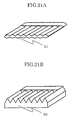
- Fig. 1 is a perspective view showing a base with linear protrusions of the present invention.
- Fig. 2 is a perspective view showing a base with dot-like protrusions of the present invention.
- Fig. 3 is a perspective view showing a base with linear protrusions and planar protrusions of the present invention.
- Fig. 4 is a perspective view showing a base with dot-like protrusions and planar protrusions of the present invention.
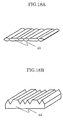
- Fig. 5A is a schematic perspective view showing a sheet
- Fig. 5B is a schematic perspective view showing a base with linear protrusions of the present invention.
- Fig. 6A is a schematic perspective view showing a sheet
- Fig. 6B is a schematic perspective view showing a base with linear protrusions of the present invention.
- Fig. 7A is a schematic perspective view showing a sheet
- Fig. 7B is a schematic perspective view showing a base with linear protrusions of the present invention.
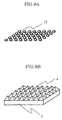
- Fig. 8A is a schematic perspective view showing a sheet
- Fig. 8B is a schematic perspective view showing a base with dot-like protrusions of the present invention.
- Fig. 9A is a schematic perspective view showing a sheet
- Fig. 9B is a schematic perspective view showing a base with dot-like protrusions of the present invention.
- Fig. 10A is a schematic perspective view showing a sheet
- Fig. 10B is a schematic perspective view showing a base with dot-like protrusions of the present invention.
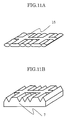
- Fig. 11A is a schematic perspective view showing a sheet
- Fig. 11B is a schematic perspective view showing a base with linear and planar protrusions of the present invention.
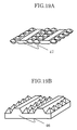
- Fig. 12A is a schematic perspective view showing a sheet
- Fig. 12B is a schematic perspective view showing a base with dot-like and planar protrusions of the present invention.
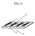
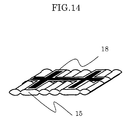
- Figs. 13 and 14 are schematic perspective views each showing a solar cell with an electrode arranged on the sheet of the present invention.
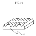
- Figs. 15 to 17 are perspective views each showing a base with linear and planar protrusions of the present invention.
- Fig. 18A is a schematic perspective view showing a sheet
- Fig. 18B is a schematic perspective view showing a base with linear and planar protrusions of the present invention.
- Fig. 19A is a schematic perspective view showing a sheet
- Fig. 19B is a schematic perspective view showing a base with dot-like and planar protrusions of the present invention.
- Fig. 20A is a schematic perspective view showing a sheet
- Fig. 20B is a schematic perspective view showing a base with linear and planar protrusions of the present invention.
- Fig. 21A is a schematic perspective view showing a sheet
- Fig. 21B is a schematic perspective view showing a base with linear and planar protrusions of the present invention.
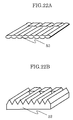
- Fig. 22A is a schematic perspective view showing a sheet
- Fig. 22B is a schematic perspective view showing a base with linear and planar protrusions of the present invention.
- Fig. 23A is a schematic perspective view showing a sheet
- Fig. 23B schematic perspective view showing a base with linear and planar protrusions of the present invention.
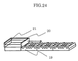
- Fig. 24 is a schematic perspective view showing a sheet manufacturing apparatus which employs a horizontal pulling method of the present invention.
- Fig. 25 is a schematic perspective view showing a sheet manufacturing apparatus which employs a rotation method of the present invention.
- Fig. 26 is a cross sectional view showing a sheet manufacturing apparatus provided with a cooling portion of the present invention.
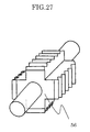
- Figs. 27 to 29 are schematic perspective views each showing a sheet manufacturing apparatus provided with a cooling portion of the present invention.
- Fig. 30 is a cross sectional view showing a general structure of the sheet manufacturing apparatus of the present invention.
- Fig. 31 is a cross sectional view showing the sheet manufacturing apparatus provided with a cooling portion of the present invention.
- Figs. 32 and 33 are cross sectional views each showing a completed silicon sheet and V grooves of the cooling roller of the present invention.
- Fig. 34 is a schematic cross sectional view showing a silicon sheet manufacturing apparatus of the present invention.
- Fig. 35 is a chart showing a manufacturing process of a solar cell according to the present invention.
- Fig. 36 is a perspective view showing a base with linear and planar protrusions of the present invention.
- the present invention is a sheet manufacturing method of directly forming on the surface of a cooled base crystals of a melt material containing at least one of a metal material and a semiconductor material and is characterized by the surface structure of the base. More specifically, the surface of the base has protrusions which are arranged in a dot-like pattern or a linear pattern when viewed from above.
- the linear protrusions refer to protrusions formed by grooves in a planar surface of the base.
- the concept of the linear protrusions include polishing and cutting formed on the surface of the base by machine processing of polishing or cutting. Namely, the linear protrusions include every protrusion in the surface of the base.
- the linear protrusions or dot-like protrusions are formed in the following manner. For example, when grooves having a width of lmm are machined in the planar surface of the base, the linear protrusions having a pitch of lmm are formed in the surface of the base. Further, the base with the linear protrusions is rotated for example by 90° and the grooves having a width of lmm are similarly formed.
- dot-like protrusions are formed having a pitch of lmm.
- the grooves in the surface of the planar base provide the linear or dot-like protrusions.
- such linear or dot-like protrusions may be polishing traces or cutting traces caused by polishing or cutting.
- the concept of the protrusions as used herein includes any protrusion in the surface of the base.
- the bases shown in Figs. 1 and 2 have protrusions in their respective surfaces.
- the base shown in Fig. 1 has linear protrusions, whereas the base shown in Fig. 2 has dot-like protrusions.
- reference numerals 1, 2, 3, and 4 respectively denote the base with protrusions, linear protrusions of the base, grooves of the base, and dot-like protrusions of the base. Note that peaks of linear protrusions 2 and dot-like protrusions 4 may be rounded.
- a sheet is formed by crystal growth on the planar base.
- crystal nuclei may be randomly produced on the base. Consequently, dendritic growth becomes dominant, resulting in large protrusions of the sheet and making it difficult to form crystals around those formed by dendritic growth.
- At least one of linear protrusion 2 and dot-like protrusion 4 facilitates removal of the sheet from the base. This is because at least one group of linear protrusion 2 and dot-like protrusion 4 enables setting/control of the starting point of crystallization (i.e., a point at which crystal nuclei is produced). Further, at least one group of linear protrusions 2 and dot-like protrusions 4 promotes nuclei production at the peak of the protrusions since such protrusion is first dipped into the melt. The protrusions provide improved removability of the sheet from the base and facilitate control of uniformity of the protrusions.
- the present invention is not particularly limited to such configuration.
- the depths of the grooves in the base are the same, while not limiting.
- the depths of the grooves may vary as necessary according to the material used.
- the bases shown in Figs. 3 and 4 have protrusions in their surfaces.
- a base 7 of Fig. 3 has linear protrusions 2 and planar protrusions 6.
- the base of Fig. 4 has dot-like protrusions 4 and planar protrusions 6.
- Planar protrusions 6 refer to protrusions formed in the surface of the base as a result of formation of grooves.
- reference numeral 6 denotes the planar protrusions.
- the protrusions have at least one of dot-like protrusions and linear protrusions, and must have planar protrusions.
- at least one of linear protrusions 2 and dot-like protrusions 4 are arranged in addition to planar protrusions 6.
- At least one group of linear protrusions 2 and dot-like protrusions 4 facilitates removal of the sheet from the base.
- Planar protrusions 6 further facilitate removability control.
- Fig. 5 is a perspective view showing a positional relationship between base 1 with linear protrusions 2 and a sheet 9 produced by crystal growth on the surface of base 1.
- a sheet produced by solidification of the melt and crystal growth on base 1 has curved portions. This is because crystals grow from linear protrusions 2 of base 1 in a curved shape. Thus, the produced sheet has curved portion.
- Crystal growth on the base occurs in the following manner. Namely, crystal nuclei are produced at peaks of linear protrusions 2 since these protrusions are first dipped into the melt. Then, since base 1 is cooled, crystal growth occurs from the crystal nuclei. The curved crystals on linear protrusions 2 grow to combine with those from adjacent linear protrusions 2, so as to produce sheet 9 with curved portions.
- the shape of sheet 9 does not conform to the protrusions of base 1 as shown in Fig. 5.
- the shape of sheet 9 is approximately as shown in Fig. 5, depending on various factors including surface tension of the melt, the temperature of the cooled base, the moving or rotating speed of the base, the shape of the protrusions and the like.
- the melt will disadvantageously proceed deeper in the grooves. In this case, removability of the sheet from the base would be impaired.
- crystal nuclei is first formed on cooled dot-like protrusion 4 and then crystal growth occurs based on the crystal nuclei. As crystal growth proceeds, crystals formed from dot-like protrusions 4 combine to form a sheet 12. Thus produced sheet 12 has curved portions.
- the moving or rotating speed of the base is high, and the melt temperature is low, rapid crystal growth occurs after formation of crystal nuclei to produce a sheet.
- Fig. 11 is a perspective view showing a positional relationship between the base with planar and linear protrusions and a sheet produced by crystal growth on the surface of the base.
- a sheet 15 produced by solidification and crystal growth of the melt on the surface of base 7 has both curved and planar portions. This is because the crystals formed from the planar protrusions of the base produce a planar portion but those formed from the linear protrusions produce a curved portion. Thus, a single sheet has both planar and curved portions.
- Crystal growth of the sheet on the base occurs as follows. Namely, crystal nuclei first produced on the planar and linear protrusions which are first dipped into the melt. Since the base is cooled down, crystal growth starts based on the crystal nuclei. The crystals in the planar shape from the planar protrusions and those in the curved shape from the linear protrusions combine together as they grow to produce a sheet with both planar and curved portions.
- resultant sheet 15 would not have the shape that conforms to the protrusions as shown in Fig. 11.
- Sheet 15 would have a shape generally as shown in Fig. 11, depending on various factors including surface tension of the melt, temperature of the cooled base, moving or rotating speed of the base, the shape of the protrusions and the like.
- crystal nuclei are first formed on the cooled planar protrusions 6 and dot-like protrusions 4, and crystal growth starts based on the crystal nuclei.
- crystals from adjacent planar protrusions 6 and dot-like protrusions 4 combine one another to form a sheet.
- the crystals formed from the linear or dot-like protrusions are curved in shape and tend to have small grain size.
- it is preferred that the planar protrusions occupy a greater percentage of the base area.
- Fig. 13 is a perspective view of sheet 9 with electrode 17 formed thereon.
- Fig. 14 is a perspective view of a sheet with a planar portion on which an electrode 18 is formed.
- Fig. 13 shows four electrodes, which are parallel to the recesses of the sheet, along with one additional electrode arranged orthogonal to these electrodes.
- the method of forming the electrode is not particularly limited to this. Namely, electrodes may be formed in the recesses of the sheet.
- Fig. 14 shows electrode 18 formed on the planar portion of the sheet. Such arrangement prevents breakage of electrode 18 and, in addition, electrode 18 on sheet 15 is not large in width.
- planar protrusions of the base produce planar portions of the sheet, so that the electrode can be readily formed thereon.
- the method of forming the electrode may employ for example screen printing, vapor deposition or plating, while not limiting.
- Reinforcing ribs of the sheet of the present invention permit usage of a method of forming an electrode with a screen mask being in contact, such as screen printing, where reduction of cost may be achieved.
- an electrode on the side of incident light (hereinafter referred to at a front electrode) is narrow, whereas a back electrode on the opposite side is formed over the entire area of the sheet.
- Both sides of the sheet with protrusions are similarly shaped and hence either side may be used as incident light side.
- the base side is preferably used as the back electrode side of the solar cell. This is because crystal nuclei are produced on linear, dot-like, and planar protrusions, resulting in extremely small crystal grains.
- a sheet manufactured by the sheet manufacturing method of the present invention is extremely effective for an electronic device which requires an electrode because the electrode can be formed directly on the planar portion.
- Sheet 15 of Fig. 14 is useful in that the base for manufacturing a solar cell may have a planar portion, which will be the light incident side to have a grid-like electrode thereon.
- a base may be manufactured from a single crystal sheet or polycrystalline sheet, such manufacture disadvantageously involves use of an oxide film, patterning by application of resist or the like, and further removal of any unwanted portion by etching.
- the sheet produced by the present invention is polycrystalline and hence includes crystal grains of various plane directions. Such variation in plane directions results in variation in etching speed during patterning, and therefore it is difficult to produce a sheet by the steps shown in conjunction with Figs. 5 to 14.
- an inexpensive sheet in a shape as shown in Figs. 5 to 14 is produced from the melt.
- a space between adjacent linear protrusions 2 of base 1 is not particularly limited.
- a constant pitch of linear protrusions 2 provides better uniformity of the sheet and is therefore more preferable.
- Even if the pitches of linear protrusions 2 are irregular, uniformity and evenness may be ensured by formation of the planar protrusions as shown in Fig. 3 or a relatively large width (area) of the planar protrusion.
- the space between the adjacent protrusions significantly governs removability of the base from the sheet. Namely, if the pitch of the linear protrusions is too small, the sheet is in contact with the base over a greater area, whereby removal of the sheet from the base requires greater force. On the other hand, if the pitch of the adjacent linear protrusions is too large, a relatively long time is required to allow crystal to grow on the base. To reduce the time required for crystal growth, the base temperature, melt temperature or the moving speed of the base must be decreased. As a result, productivity decreases. Note that the pitch of the adjacent dot-like protrusions significantly governs removability of the sheet from the base.
- the pitch of the adjacent planar protrusions 6 as shown in Figs. 3 and 4 is not particularly limited, greater width (area) of planar protrusions 6 provides better evenness of the sheet.
- relatively large width (area) of planar protrusions 6 tends to decrease removability of the sheet from the base, and therefore the width (area) of planar protrusions 6 must be properly selected.
- bases of Figs. 3 and 4 have linear or dot-like protrusions between the adjacent planar protrusions 6, the numbers thereof are not particularly limited, and the protrusions can be designed as appropriate considering evenness, removability or the like.
- the pitch of the linear protrusions is preferably at least 0.05mm.
- the pitch of the dot-like protrusions is also preferably at least 0.05mm.
- a pitch less than 0.05mm results in disadvantageously small crystal grains that impair the properties of the solar cell, and is not desirable.
- the recesses shown in Figs. 1 to 4 are in the shape of V like grooves, the recesses may be in the shape of V as shown in Figs. 15 to 17, U, trapezoid, oblique groove and the like, and are not particularly limited.
- Bases having linear and linear protrusions with U grooves, trapezoidal grooves and oblique grooves are respectively denoted by reference numerals 41, 42 and 43.
- the depth of the groove is at least 0.05mm and, more preferably, at least 0.1mm. A depth of the groove less than 0.05mm would make it difficult to remove the produced sheet from the base due to crystal growth at the groove.
- the depth of the groove must be appropriately selected in consideration of the structure of the base and the melt material since surface tension of the melt material may also determine the resulting effect.
- the grooves are shown in the drawing as having the same depth, they may have different depths. This is because the temperature more or less varies over the surface of the base according to the depth of the groove when the base is cooled. Thus, the surface shape and the depth of the groove must be appropriately determined for temperature control.
- planar protrusions 6 are arranged orthogonally in Figs. 3 and 4, they may not be orthogonal.
- Figs. 18 to 23 show schematic illustrations of a sheet obtained when the planar protrusions are not orthogonally arranged.
- Bases with protrusions are denoted by 44, 46, 48, 50, 52, and 54, whereas sheets resulting from these bases are denoted by 45, 47, 49, 51, 53 and 55.
- planar protrusions may be arranged in parallel as shown in Figs. 18 and 19. They may be arranged in parallel with the grooves as shown in Fig. 20. They may be formed orthogonally to the grooves as shown in Figs. 21 and 22. Grooves may be partially formed as shown in Fig. 23.
- the planar protrusions are orthogonally arranged. This is because the maximum possible current must be derived to improve the properties of the solar cell. More specifically, orthogonal arrangement of a bus bar electrode (main electrode) and a finger electrode (sub electrode) facilitates designing to reduce series resistance.
- the width of the planar protrusion is designed to reduce the series resistance.
- the portion to be the bus bar electrode has a larger width
- the portion to be the finger electrode has a smaller width.
- the protrusions of the base act as basis for crystal growth of the sheet, and crystal growth depends on the shape, width and pitch of the protrusions, the melt material, the melt temperature, base material, base temperature and the like. Therefore, it is preferable that these factors are appropriately determined.
- a material with excellent heat conductivity and heat resistance is used for the base with protrusions.
- materials used for the base include high-purity graphite, silicon carbide, quartz, boron nitride, alumina, zirconium oxide, and metal. The optimum material may be selected according to the melt used.
- High-purity graphite is more preferable because of its inexpensiveness and workability, which facilitate formation of protrusions.
- the material for the base can be appropriately selected by considering industrial inexpensiveness, various properties such as a base property of the produced sheet and the like, for determining the combination of the melt material and the base.
- Metal may be used for the base without causing any problem, as long as constant cooling is maintained, temperature of the metal is maintained below a melting point of the base, and it does not adversely affect the properties of the sheet.
- the base can be cooled either by direct or indirect cooling.
- a base is directly cooled by gas.
- the base is indirectly cooled by gas or melt.
- inert gas such as nitrogen, argon, or helium is preferred.
- Helium or mixture gas of helium and nitrogen is preferred particularly in terms of cooling ability, but nitrogen is preferable in terms of cost.
- the coolant gas is circulated with use of a heat exchanger or the like, for cost reduction.
- a sheet manufacturing apparatus using a base with protrusions will be described.
- a method of forming a sheet onto a continuous base having continuously arranged bases will be described.
- a continuous base having protrusions is denoted by 19, a crucible by 20, and a melt by 21.
- the melt in the crucible is heated to at least a melting point by a heater and maintained in a stable melt state.
- the melt include semiconductor materials such as silicon, germanium, gallium, arsenic, indium, phosphorus, boron, antimony, zinc, tin, or a melt including metal material such as aluminum, nickel, or iron.
- the bottom of crucible 20 has an opening, through which melt 21 can be continuously supplied onto continuous base 19. Crystals grow on continuous base 19 to form a sheet.
- melt 21 can be continuously supplied onto continuous base 19. Crystals grow on continuous base 19 to form a sheet.
- Fig. 25 is a schematic diagram showing a sheet manufacturing apparatus provided with a movable roller.
- a movable roller is denoted by 22, and protrusions in the surface thereof are denoted by 23.
- the protrusions include both linear and planar protrusions here.
- the roller is shown as having protrusions in its surface, these protrusions may be removably attached to the surface of the roller. Protrusions extend outwardly with respect to a rotation axis of the roller on the peripheral surface of the roller.
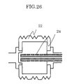
- Fig. 26 is a cross sectional view showing a cooling portion of the sheet manufacturing apparatus with a roller having the cooling system.
- Coolant gas nozzle is denoted by 24.
- Coolant gas nozzle 24 serves to gradually cool from inside roller 22, for indirectly cooling protrusions in the surface of roller 22.
- Such indirect cooling of protrusions enables continuous production of the sheet.
- a cooling means inside roller 22 may be any means so long as it uniformly cools the base mounted on the roller. Namely, a structure of cooling by gas or melt is preferred.
- inert gas such as nitrogen, argon, or helium is used as coolant gas. While helium or mixture gas of helium and nitrogen is preferred in terms of cooling ability, nitrogen is more preferable in terms of cost. Further, coolant gas or water is circulated with use of a heat exchanger or the like for cost reduction.
- Figs. 26 and 31 show linear and planar protrusions formed in the surface
- Fig. 31 shows only linear protrusions formed in the surface. While not shown in the drawings, dot-like protrusions may be formed.
- the cooling roller being cylindrical in shape, has been described in the above. Now, polygonal cooling roller will be described. In this case, since the side for crystal growth is planar, a planar sheet is obtained. Thus, a polygonal roller is extremely effective for the purpose of manufacturing solar cells.
- Fig. 27 is a schematic diagram showing a sheet manufacturing apparatus provided with a movable polygonal roller.
- the roller with linear protrusions is denoted by 56.
- the roller is shown as having four sides adapted to be used for crystal growth of the sheet, the roller may not necessarily have four sides.
- a roller with a large diameter is preferably employed so that one rotation provides a plurality of sheets.
- Fig. 27 shows linear protrusions formed on the roller having planar surfaces. In this case, the linear protrusions are arranged in the rotation direction of the roller.
- Fig. 28 shows linear protrusions formed orthogonal with respect to the rotation direction of the roller.
- a roller with linear protrusions is denoted by 57.
- linear protrusions are preferably formed in the same direction as the rotation direction of the roller. If the linear protrusions are in the rotation direction, the melt more easily spread over the surface of the base with protrusions. In other words, the melt can move smoothly over the surface, thereby preventing formation of a rough sheet due to thickened melt not spread smoothly.
- the grooves may be formed such that protrusions converge in one point to collect the melt. As shown in Fig. 36, for example, the oblique grooves collect the melt at the central portion.
- the above described polygonal roller may have protrusions in the base as shown in any of Figs. 1 to 4 and Figs. 15 to 23. Even in the case of Fig. 28, a sheet can be manufactured without having any protrusions. This is because the grooves in the surface as well as the spaces between the planar sides of the polygonal body can be controlled to provide desired shapes.
- the shapes of the protrusions in the base can be designed in consideration of the shape of the sheet to be produced, regardless of whether or not the base moves.
- a high-purity coating may be applied to the surface of the base with protrusions. Further, a high-purity coating may be applied to the surfaces of the protrusions.
- the coating material includes at least one of silicon carbide (SiC), boron nitride (BN) silicon nitride (SiNx), and pyrolitic carbon. Namely, the presence of the high-purity coating on the surface of the base prevents contamination of the sheet.
- silicon carbide, silicon nitride, pyrolitic carbon or the like can be used.
- a coating containing at least one material on the protrusions can prevent the melt from being poured into the grooves of the protrusions.
- a material with low wettability with respect to the silicon melt prevents such melt from entering the grooves. Even in the case of a material with high wettability with respect to the silicon melt such as pyrolitic carbon, if the material is formed in layers, the sheet can be readily removed from the base even under the condition that the sheet adheres to the planar surface, because of the protrusions in the surface of the base and the layered structure.
- thermal expansion coefficients of these materials do not differ largely. This is because the difference in thermal expansion coefficient between the surface of the base to be subjected to high temperature and the base to be cooled may cause a coating to come off.
- a high-quality sheet can be obtained by appropriately controlling the material or thickness of the coating on the surfaces of the protrusions.
- the sheet thus formed can be cut to have a desired size (length) with use of a microcutter, YAG laser or the like, or directly used as it is.
- Fig. 29 shows a schematic diagram of an internal portion of the sheet manufacturing apparatus with the roller
- a crucible is denoted by 25
- a crucible table with an elevator is denoted by 26
- a heater for temperature adjustment is denoted by 27.
- Crucible 25 containing the melt is disposed on crucible table 26.
- the roller having a cooling portion is arranged above the crucible table. In the drawing, it can be seen that linear protrusions are formed in the rotation direction in the surface of the roller so as to be dipped into the melt in the crucible.
- FIG. 30 of a schematic diagram which shows the sheet manufacturing apparatus, the method of manufacturing the sheet will be described.
- a pipe for additionally introducing material, a heat-resisting material, a chamber, and a guide roller for transportation of sheet are respectively denoted by 28, 29, 30, and 31.
- a cylindrical roller is employed herein, a polygonal roller as shown in Figs. 27 and 28 may be employed.
- the surface structure of the roller may be as shown in any of Figs. 1 to 4 and Figs. 15 to 23.
- the sheet manufacturing apparatus is provided in a tightly closed chamber 30 and gas exchange is performed with use of inert gas after evacuation.
- inert gas examples include argon and helium, where argon is more preferable in terms of cost.
- heat-resisting material 29 and a plurality of heaters for temperature adjustment 27 are arranged in chamber 30 to accurately control the melt temperature. Accurate control of the ambient temperature in chamber 30 and the melt temperature enables the sheets to be produced stably with higher reproducibility.
- the temperature of the melt is, preferably, at least the melting point of the metal material or the semiconductor material. If the temperature of the melt is near the melting point, when the cooled base is dipped in the melt, the melt surface may be coagulated.
- crucible table 26 is preferably provided with an elevator, so as to maintain the base in the melt at the same depth for forming the sheet on the base.
- polycrystalline body of the same material as the melt is molten or powder is sequentially added with use of pipe 28.
- the method of maintaining the level of the melt is not particularly limited. Note that fluctuation of the surface of the melt should be minimized. This is because the fluctuation of the surface of the melt may impair uniformity of the resultant sheet.
- Fig. 31 is a cross sectional view of a cooling roller of the present embodiment.
- the cooling roller of the present embodiment has protrusions in its surface.
- the protrusions are in the shape of V or U groove, and arranged in a dot-like pattern or a linear pattern.
- the silicon sheet is produced from the protrusions by solidification and crystal growth, and can be readily and continuously pulled out. The detailed description is given in the following.
- reference numerals 32, 33, 34, and 35 respectively denote a cooling roller, a peak of the V groove of the cooling roller (a top portion of the protrusion of the cooling roller), a trough of the V groove, and gas nozzle for introducing coolant gas.
- Any material can be used for cooling roller 32 if it has resistance to high temperature. Examples of the material include molds of high-purity carbon, fire-resisting ceramics, silicon nitride, and boron nitride. The carbon material is, preferably, inexpensive and has high workability. A metal material may also used for cooling roller 32.
- Any material may be used without any problem, which has a melting point higher than that of silicon and which does not adversely affect the semiconductor properties of the resultant silicon sheet. Even when the metal material has a melting point lower than that of silicon, if coolant gas or water is supplied to maintain the temperature below the melting point of that metal, such metal material can be used without causing any particular problem.
- a plurality of peaks 33 of V grooves are arranged in an annular manner in the surface of cooling roller 32, having a prescribed pitch and depth.
- the cooling roller has a hollow shape for the coolant gas or water.
- Gas nozzle 35 is coaxially provided inside cooling roller 32, which is adapted to direct externally supplied coolant gas toward the peaks 33 of V grooves.
- the type of the coolant gas is not particularly limited since it is not brought into direct contact with the silicon melt, preferably, the coolant gas is an inert gas such as N 2 , He, or Ar. He or a mixture of He and N 2 is preferable in terms of cooling ability, whereas N 2 is preferable in terms of cost.
- the coolant gas After cooling roller 1 from inside, the coolant gas is exhausted.
- the evacuated gas after cooling roller 1 may be circulated by an externally provided heat exchanger (not shown) for further reduction of cost.
- cooling roller 32 of the present embodiment has in its surface V grooves as shown in Fig. 31. Greater thickness of the peaks and troughs of the V grooves of cooling roller 32 may provide enhanced cooling effect. Note that a greater surface area, for example achieved by provision of protrusions inside cooling roller 32, can further enhance cooling effect. Namely, it is preferable to increase the contact area of the coolant gas by providing protrusions inside cooling roller 32.
- Cooling roller 32 is dipped into the silicon melt to form a silicon sheet on its surface. As shown in Fig. 32, cooled peaks 33 of V grooves are dipped into the silicon melt, so that the crystal nuclei of silicon are first produced at the peaks 33 of the V grooves. Crystal growth starts from based on the crystal nuclei. As crystal growth proceeds, the silicon crystals from adjacent peaks 33 of the V grooves combine to produce a silicon sheet 60.
- the resultant silicon sheet has curved portions on the melt side. Namely, the portions where the crystal nuclei are first formed correspond to the peaks of the V or U grooves of cooling roller 32, and the silicon crystals which grow therefrom are sufficiently cooled in an initial stage of crystal growth.
- the shape of the sheet generally reflects the surface structure of the cooling roller. However, the sheet may not conform to the surface structure of the cooling roller completely, when removability is considered. If the silicon sheet conforms completely to the surface structure of the cooling roller 32, it means that the sheet tightly adheres to cooling roller 32. Thus, a silicon sheet with sufficient removability is not obtained.
- the silicon melt On the melt side, the silicon melt is, partially, not completely cooled and still remains in the melt state. Such silicon provides curved portions with its force of gravity. Thus, a silicon sheet in a specific shape of the present invention is produced. In this method, an inexpensive silicon sheet can be provided because the slicing loss is saved and the curved portions provide corresponding reduction in the amount of silicon used.
- corrugated or wave-like silicon sheet can be directly formed on the cooling roller under manufacturing conditions of the silicon sheet.
- the silicon sheet has a feature on the side in contact with the cooling roller, in addition to the feature of the curved portions on the melt side.
- the crystal nuclei of silicon produced at the peaks of the V or U grooves of cooling roller 32 rapidly grow. Then, crystal growth of silicon starts, and the direction of crystal growth is determined by the cooling ability of the coolant gas or the rotating speed of cooling roller 32. If the cooling ability of the coolant gas is sufficient, the rotating speed of the roller 32 is high, and the melt temperature is low, silicon crystals grow after the crystal nuclei are produced along peaks 33 if the V or U grooves of cooling roller 32 in the direction toward the melt side, as shown in Fig 32.
- the surface structure of the cooling roller and the silicon sheet would not completely conform to each other as shown in figs 32 and 33. If the surface structure of the cooling roller completely conform to the silicon sheet, adhesion strength between the surface of the cooling roller and the silicon sheet is high, whereby removal becomes difficult. Thus, it is not desirable for serial production. As described above, by appropriately determining the conditions, a silicon sheet in a desired shape can be produced.
- a silicon sheet in a corrugated or wave-like shape can be manufactured with use of a silicon wafer, such manufacture involves patterning by application of an oxide film or resist and subsequent etching.
- the resultant silicon sheet is polycrystalline, and therefore crystal grains of various plane directions exist.
- a silicon sheet can be obtained inexpensively in this method of directing forming the silicon sheet in the corrugated or wave-like shape from the silicon melt.
- the melt side has curved portions as in the present invention.
- cooling roller 32 rotates with gas nozzle 35 shown in Fig. 31 fixed. If gas nozzle 35 rotates with cooling roller 32, the same portion is always cooled, whereby it becomes difficult to uniformly form the silicon sheet on the surface of cooling roller 32.
- Such a structure enables the internal portion of cooling roller 32 to be uniformly cooled, so that a uniform silicon sheet can be produced.
- gas nozzles 35 are shown in Fig. 31 being above each other, the arrangement is not particularly limited to this.
- a plurality of gas nozzles 35 are arranged in radial directions rather than in one direction.
- the crystal nuclei can be produced more effectively on the surface of cooling roller 32, so that a uniform silicon sheet can be produced.
- an SiC film is formed on the surface of the V or U grooves in cooling roller 32.
- cooling roller 32 is formed of graphite
- crystal nuclei of silicon are produced on a graphite surface, and therefore the silicon sheet would be produced on the graphite surface.
- graphite may come off with the silicon sheet.
- the graphite adhering to the silicon sheet may be readily removed by etching with use of a mixture of nitric acid and hydrofluoric acid, but the number of processes cost increase.
- a cooling roller of graphite is used, such roller is formed by cutting and shaping a graphite mold. It is almost impossible to completely remove the resulting cutting chips. The chips may fall into the silicon melt, thereby causing a problem associated with contamination of the silicon melt.
- the surface of the cooling roller is coated with an SiC film or the like.
- the SiC film is preferably formed of a ceramic film, for which a technique for forming a high-purity film is available.
- Cooling roller 32 has in its surface V or U grooves, on which the SiC film is formed. As such, the SiC film at the peaks of the V or U grooves is dipped in the silicon melt. More specifically, the crystal nuclei of silicon are produced on the SiC film for production of the silicon sheet. Thus, the contact area of the cooling roller 32 and the silicon sheet becomes extremely small, whereby the adhesion strength of the silicon sheet and the cooling roller decreases. As a result, removability of the silicon sheet from cooling roller 32 improves.
- a pitch of the V or U grooves in the surface of cooling roller 32 is at least 0.05mm and at most 5mm. If a pitch is smaller than 0.05mm, silicon crystals begin to grow from peaks 33 of the V grooves to combine with those from adjacent peaks 33 at troughs 34 of the V grooves. As a result, the crystal grain size of the silicon sheet would be about half the pitch. Thus, the pitch smaller than 0.05mm is not desirable when the sheet is to be used for a solar cell.
- a greater number of peaks of V or U grooves increases the adhesion area of the silicon to cooling roller 32. As a result, the adhesion strength of the silicon sheet and the cooling roller increases, whereby removal becomes difficult.
- a pitch of the grooves is greater than 5mm, on the other hand, a longer time is required for the silicon crystals growing from peaks 33 to combine with one another to form a silicon sheet. In such a case, for example, the rotating speed of cooling roller 32 needs to be decreased. As a result, productivity decreases and inexpensive silicon sheet cannot be provided.
- the depth of the V or U grooves of cooling roller 32 is at least 0.05 and at most 5mm.
- the height determines the dipping depth of cooling roller 32. More specifically, a greater depth allows the greater portion of the protrusions to be dipped into the melt, and vice versa.
- the silicon crystals grow in the silicon melt or near the surface of the silicon melt.
- the dipping depth needs to be appropriately determined as it determines the thickness of the sheet to be produced.
- the V or U groove in the surface of the cooling roller allows the crystal grain size or silicon sheet thickness to be relatively readily controlled.
- the crystal grain size or silicon sheet thickness also depends on the temperature of a heater, the flow rate of coolant gas flowing through the cooling roller, the rotation speed of the cooling roller and the like, which can be appropriately determined to provide a silicon sheet with a desired thickness.
- a bar-like remover can be arranged in a mechanism for pulling out the produced silicon sheet. Since cooling roller 32 has V or U grooves, it is possible to arrange the leading end of the bar-like remover along trough 34.
- the shape of the remover may be for example in a comb, bar or polygon-like shape, while not limiting. It is preferred that its shape conforms to trough 34 and the height of the remover is smaller than the depth of the V or U grooves. Namely, any shape may be employed which conforms to trough 34 of cooling roller 32 and not is not dipped into the silicon melt.
- Such a structure enables the silicon sheet to be easily and continuously pulled out without complicating the apparatus. There is no need to stop the operation of the apparatus even if the silicon crystals break or fall during crystal growth, such silicon crystals simply fall down into the melt, whereby continuous operation is enabled.
- the material for the remover may include a mold body of carbon, ceramics, tungsten, silicon nitride, boron nitride or the like, which are all materials stable in an inert ambient at high temperature, while not limiting. It is preferably the same material as the cooling roller because such material is maintained at the high temperature as being near the silicon melt and because such material does not cause damage to the surface of the cooling roller. Any shape conforming to the shape of the V or U groove may be employed, and the shape of the remover is limited to the bar-like shape. It may also be in a fork-like shape.
- V or U groove in the surface of cooling roller 32 and a remover conforming thereto enables the produced silicon sheet to be readily removed from the cooling roller.
- the removed silicon sheet is transported by a guide roller to outside the chamber.
- produced silicon sheet is cut by a microcutter, YAG laser or the like to have a desired size (length) and to provide silicon wafers.
- Fig. 34 shows a general structure of a silicon sheet manufacturing apparatus.
- a silicon melt, crucible, heater for temperature control, guide roll for transportation, and silicon sheet are respectively denoted by reference numerals 36, 37, 38, 39, and 40.
- the silicon sheet manufacturing apparatus is arranged in a tightly sealed chamber, and gas exchange is performed by inert gas after evacuation.
- the gas may be for example Ar or He, but Ar is more preferable in terms of cost.
- a plurality of heaters are arranged in the chamber for accurately controlling the temperature of the silicon melt. Accurate control of the temperature of the silicon melt enables the production of the silicon sheet with sufficient reproducibility.
- the temperature of the silicon melt is preferably at least the melting point of the silicon (about 1420°C). Near the melting point, the dipping of the cooled roller into the melt may cause solidification at the surface of the melt, and therefore the melt temperature is preferably maintained at 1430°C or higher.
- the crucible containing the melt silicon may be provided with an elevator. This is because the cooling roller must be dipped into the silicon melt always at the same depth to produce the silicon sheet on the cooling roller.
- the method of maintaining the position of the surface of the melt at the same level may include, for example, melting polycrystalline silicon ingot or introduction of silicon powders, while not limiting. However, it is preferable that fluctuation of the surface of the silicon melt is minimized.
- a silicon sheet is manufactured.
- a silicon material with boron concentration adjusted to have resistivity of 2 ⁇ cm was introduced into a crucible of quartz, which was protected by a crucible formed of high-purity carbon.
- the crucible was fixed in a chamber as shown in Fig. 30.
- the chamber was evacuated to have a pressure at or below 2 ⁇ 10 -5 torr. Thereafter, Ar gas was introduced to the chamber and the pressure was recovered to an atmospheric pressure. Subsequently, a flow of Ar gas was maintained from above the chamber, with a flow rate of 2L/min.
- the temperature of the heater for melting silicon was set at 1500°C and silicon was completely brought into a molten state.
- the melt surface was lowered as the silicon material melts.
- a silicon material was added by a pipe for introducing additional silicon material to maintain the position of the surface at a prescribed level.
- the temperature of the silicon melt was set at 1430°C, which temperature was maintained for 30 minutes for stabilization.
- nitrogen gas was sprayed to the internal portion of the roller with a flow rate of 700L/min for cooling.
- a base having linear and planar protrusions as shown in Fig. 3 was used.
- a pitch of linear protrusions was lmm and a width of planar protrusions was lmm.
- the depth of grooves was lmm and the outer dimension of the base was 50mm ⁇ 50mm.
- a polygonal roller as shown in Fig. 27 was employed.
- the quartz crucible was gradually elevated until it reaches the position allowing the base to be dipped into the melt by 3mm.
- the roller was rotated at 0.5rpm for producing a silicon sheet.
- the crucible table was lowered and dipping was stopped.
- the silicon sheet was pulled out when the chamber temperature was lowered to the room temperature. Then, the produced silicon sheet could be readily removed from the base.
- the silicon sheet had substantially the same size as the base, i.e., 50mm ⁇ 50mm.
- the produced silicon sheet was substantially in the shape as shown in Fig. 11, where the maximum thickness was about 0. 4mm and the minimum thickness was about 0.25mm.
- a solar cell was manufactured.
- the silicon sheet was etched by a solution of nitric acid and hydrofluoric acid and cleaned.
- alkali etching was performed by sodium hydroxide.
- an n layer was formed on a p type substrate by diffusion of POCI 3 .
- a silicon nitride film was formed on the n layer which was to be front side of the solar cell by plasma CVD.
- the n layer formed on the back side of the solar cell was etched and removed by a solution of nitric acid and hydrofluoric acid to expose the p substrate.
- the back electrode and a p+ layer are formed thereon at the same time.
- an electrode on the light receiving side was formed by screen printing.
- screen printing was performed such that the electrode was formed on the planar portion of the silicon sheet as shown in Fig. 14.
- solder dipping was performed to complete a solar cell.
- Thus manufactured solar cell was measured for its properties under irradiation condition of AM1.5, 100 mW/cm 2 .
- the results were short-circuit current of 30.3 (mA/cm 2 ), open-circuit voltage of 590 (mV), fill factor of 0.69, and efficiency of 12.3 (%).
- a silicon sheet and solar cell were manufactured in accordance with the same method as in the first embodiment except that the surface structure of the polygonal roller included only linear protrusions as shown in Fig. 1.
- a pitch of the linear protrusions of the base was lmm and the depth of the grooves was lmm.
- the surface of the sheet did not have any planar portion, so that a sub electrode was formed in parallel with the groove as shown in Fig. 13.
- the silicon sheet was in the same shape as in Fig. 5, where the thickness of the sheet was about 0.5mm and the manufactured solar cell showed the following measurement results: short-circuit current of 28.3 (mA/cm 2 ), open-circuit voltage of 580 (mV), fill factor of 0.61, and efficiency of 10.0(%).
- a silicon sheet and a solar cell were manufactured in the same method as in Embodiment 1 except that the surface structure of the polygonal roller included only dot-like protrusions as shown in Fig. 2.
- a pitch of the dot-like protrusions of the base was 0.1mm and the depth of the grooves was 0.1mm.
- the produced sheet did not have any planar portion, so that an electrode was formed in parallel with the sides of the base.
- the produced sheet was in the same shape as in Fig. 8, having a thickness of about 0.5mm.
- the manufactured solar cell showed the following measurement results: short-circuit current of 29.8 (mA/cm 2 ), open-circuit voltage of 587 (mV), fill factor of 0.67, and efficiency of 11.7 (%).
- a silicon sheet and solar cell were manufactured in the same method as in the first embodiment except that the surface structure of the polygonal roller had only dot-like protrusions and planar protrusions as shown in Fig. 4.
- a pitch of the dot-like protrusions of the base was 1.5mm and the width of the planar protrusions was lmm. The depth of the grooves was 0.5mm.
- the produced sheet was in the shape as shown in Fig. 12, having the thickness of about 0. 3mm.
- the manufactured solar cell showed the following measurement results: short-circuit current of 30.4 (mA/cm 2 ), open-circuit voltage of 588 (mV), fill factor of 0.69, and efficiency of 12.3 (%).
- a silicon sheet and a solar cell were manufactured in the same method as in the first embodiment except that the flow rate of the coolant gas in the polygonal roller was 1200 L/min.
- the produced silicon sheet was in the shape shown in Fig. 11, having a thickness of about 0.5mm.
- the manufactured solar cell showed the following measurement results: short-circuit current of 29.9 (mA/cm 2 ), open-circuit voltage of 588 (mV), fill factor of 0.68, and efficiency of 12.0 (%).
- a silicon sheet and a solar cell were manufactured in the same method as in the first embodiment except that the flow rate of the coolant gas in the polygonal roller was 500L/min.
- the produced silicon sheet was in the shape as shown in Fig. 11, having a thickness of about 0.7mm.
- the manufactured solar cell showed the following measurement results: short-circuit current of 30.1 (mA/cm 2 ), open-circuit voltage of 590 (mV), fill factor of 0.68, and efficiency of 12.1 (%).
- a silicon sheet was manufactured in the same method as in the first embodiment except that the flow rate of the coolant gas in the polygonal roller was 50L/min.
- the produced silicon sheet was in a shape similar to that shown in Fig. 11, but the silicon sheet could not be removed from the polygonal roller. Thus, a solar cell could not be manufactured.
- a silicon sheet was manufactured in the same method as in the first embodiment, and a solar cell was manufactured in the same method as in the first embodiment except that an electrode was formed in the portion other than the planar portion.
- the produced sheet has a thickness of about 0. 5mm, and the manufactured solar cell showed that following measurement results: short-circuit current of 29.1 (mA/cm 2 ), open-circuit voltage of 585 (mV), fill factor of 0.64, and efficiency of 10.9 (%).
- a silicon sheet was manufactured in the same method as in the first embodiment except that the surface structure of the polygonal roller had only a planar portion, free of protrusions, and a solar cell was also manufactured.
- the silicon sheet was mainly formed by dendritic growth and the surface structure of the produced silicon sheet was uneven.
- the manufactured solar cell showed the following measurement results: short-circuit current of 28.3 (mA/cm 2 ), open-circuit voltage of 580 (mV), fill factor of 0.65, and efficiency of 10.7 (%).
- a silicon sheet was manufactured.
- a silicon material of which boron concentration has been adjusted to have resistivity of 0.5 ⁇ cm was introduced to a crucible of quartz protected by a high-purity carbon crucible. The crucible is then fixed in a chamber as shown in Fig. 30.
- the chamber was evacuated to have a pressure at or below 2 ⁇ 10 -5 torr. Then, Ar gas was introduced into the chamber and the pressure was recovered to an atmospheric pressure. Subsequently, Ar gas was allowed to flow from above the chamber at 2 L/min. Then, the temperature of a heater for melting silicon was set at 1500°C to completely bring the silicon into a molten state. At the time, the silicon material melts and hence decreases its surface level. Thus, the silicon material is further introduced by a pipe to adjust the surface level to a prescribed position. Then, the temperature of the silicon melt is set at 1450°C and maintained thereat for 30 minutes for stabilization. Then, nitrogen gas is sprayed to the internal portion of the roller at 1000 L/min without rotating the roller for cooling.
- a cylindrical roller having a surface structure including linear and planar protrusions as shown in Fig. 4 was used.
- a pitch of dot-like protrusions was 2mm
- a width of the planar protrusions was lmm
- the roller had a diameter of 800mm.
- the quartz crucible was gradually elevated up to a level where the base was dipped into the melt by 4mm, where the roller was rotated at 5rpm for production of the silicon sheet.
- the crucible table was lowered to stop heating.
- the silicon sheet was pulled out when the chamber attains to a room temperature. In this case, the silicon sheet could readily be removed from the base.
- the silicon sheet was cut to have a size of 50mm ⁇ 40mm.
- the silicon sheet was in the shape as shown in Figs. 12, where the maximum thickness was about 0.3mm and the minimum thickness was about 0.2mm.
- a solar cell was manufactured using the produced silicon sheet.
- the produced silicon sheet was etched and cleaned using a solution of nitric acid and hydrofluoric acid and then subjected to alkali etching using sodium hydroxide. Thereafter, an n layer formed on a p type substrate by diffusion of POCI 3 .
- a PSG film formed on the surface of the sheet was removed by hydrofluoric acid, and a silicon nitride film was formed on the n layer to be a light receiving side of the solar cell by plasma CVD.
- the n layer formed on the back side of the solar cell was etched and removed by a solution of nitric acid and hydrofluoric acid, and the back electrode and p+ layer were formed at the same time.
- a silicon sheet was manufactured by the same method as in the seventh embodiment except that the rotating speed of a cylindrical roller was 15rpm.
- the produced silicon sheet had holes, because crystals were not formed at the grooves of the sheet.
- a silicon sheet and a solar cell were manufactured in the same method as in the seventh embodiment except that the surface structure of the cylindrical roller had only linear and planar protrusions as shown in Fig. 18.
- a pitch of the linear protrusions of the base was 2mm, a depth of the grooves was 0.1mm, and width of the planar protrusion was 10mm.
- the produced silicon sheet was in the shape as shown in Fig. 18, having a thickness of about 0.4mm.
- the manufactured solar cell showed the following measurement results: short-circuit current of 29.8 (mA/cm 2 ), open-circuit voltage of 588 (mV), fill factor of 0.68, and efficiency of 11.9 (%).
- a silicon sheet and a solar cell were manufactured in the same method as in the seventh embodiment except that the surface structure of the cylindrical roller had only dot-like protrusions and planar protrusions as shown in Fig. 19.
- a pitch of the linear protrusions of the base was 2mm, a depth of the grooves was lmm, and a width of the planar protrusions was 10mm.
- the produced silicon sheet was in the shape as shown in Fig. 19, having a thickness of about 0.4mm, the manufactured solar cell showed the following measurement results: short-circuit current of 29.9 (mA/cm 2 ), open-circuit voltage of 589 (mV), fill factor of 0.67, and efficiency of 11.8 (%).
- a silicon material of which boron concentration has been adjusted to have resistivity of 1 ⁇ cm was introduced into a crucible of quartz protected by a high-impurity carbon crucible and brought into a molten state. Then, as shown in Fig. 24, a crucible having at its bottom an opening is placed on the base with protrusions.
- the base with linear and planar protrusions as shown in Fig. 3 was used.
- a pitch of the linear protrusions was 2mm, a width of the planar protrusions was 2mm, and a depth of the grooves was 0.1mm.
- the base with protrusions was cooled down with a flow rate of coolant gas of 500L/min.
- molten silicon is introduced into the crucible and, at the same time, the crucible is moved at a speed of 1m/min to produce a silicon sheet.
- the produced silicon sheet was substantially the same as the base in size, having 50mm ⁇ 50mm.
- the produced silicon sheet had the maximum thickness of about 0.3mm and the minimum thickness of about 0. 15mm.
- a solar cell was manufactured with use of the produced silicon sheet.
- the produced silicon sheet was subjected to alkali etching using sodium hydroxide.
- an n layer was formed on a p type substrate by diffusion of POCl 3 .
- the PSG film formed on the surface of the sheet was removed by hydrofluoric acid, and a TiO 2 film was formed on the n layer on the front side of the solar cell.
- the n layer formed on the back side of the solar cell was etched and removed by a solution of nitric acid and hydrofluoric acid to expose the p substrate, on which the back electrode and p+ layer were simultaneously formed.
- an electrode on the front side was formed by screen printing.
- the screen printing was performed to form an electrode at the planar portion of the silicon sheet. Then, solder dipping was performed to produce a solar cell.
- the produced solar cell was measured for its cell properties under irradiation conditions of AM1.5, 100 mW/cm 2 . The measurement results showed short-circuit current of 25 (mA/cm 2 ), open-circuit voltage of 571 (mV), fill factor of 0.65, and efficiency of 9.3 (%).
- a sheet was manufactured in the same method as in the tenth embodiment except for usage of nickel.
- the produced nickel sheet was in the shape as shown in Fig. 11, having a thickness of about 0. 4mm.
- a sheet was manufactured in the same method as in the tenth embodiment except for usage of aluminum and the base of Fig. 2.
- a pitch of dot-like protrusions was lmm, and a depth of the grooves was 0.6mm.
- the produced aluminum sheet was in the shape as shown in Fig. 8, having a thickness of about 0.3mm.
- the base of the cooling roller had V grooves, for the purpose of observing variation in the shape of the silicon sheet according to the rotating speed.
- High-purity silicon (purity of 99.999999999%) and, as a dopant thereof, a master alloy with boron, were prepared.
- a silicon material of which boron concentration had been adjusted to have resistivity of 2 ⁇ cm was introduced into a quartz crucible protected by a high-purity carbon crucible.
- the crucible was fixed in a chamber (chamber wall is not shown) of the apparatus shown in Fig. 34.
- the chamber was evacuated to attain a pressure at or below 2 ⁇ 10 -5 torr.
- Ar gas was introduced into the chamber so that the chamber attained an atmospheric pressure. Subsequently, a flow of Ar gas was maintained from above into the chamber at 2L/min.
- the temperature of a heater for melting silicon is set at 1500°C to bring silicon completely in a molten state.
- silicon material melted its surface level significantly decreased.
- additional silicon material is introduced to adjust the surface of the melt at a prescribed level.
- the silicon melt temperature is set at 1430°C, which temperature is maintained for 30 minutes for stabilization.
- Nitrogen gas is sprayed to the internal portion of the cooling roller at a flow rate of 700 L/min without rotating the cooling roller having a SiC film of 10 ⁇ m.
- a pitch of the V grooves of the cooling roller then used was lmm, and a depth of the grooves was 1mm.
- the quartz crucible was gradually elevated to a level where the peaks of the V grooves of the roller were dipped into the melt by 3mm.
- the roller was rotated at a rotating speed of 0.5rpm, 5rpm, and 10rpm to produce a silicon sheet.
- the resultant silicon sheet had a thickness and average crystal grain size as shown in the following Table 1.
- ROTATING SPEED rpm
- THICKNESS ⁇ m
- GRAIN SIZE mm
- the thickness of the silicon sheet as well as average crystal grain size decrease. Namely, by controlling rotation of the cooling roller, the thickness of the silicon sheet formed on the cooling roller can readily be controlled.
- the shape of the produced silicon sheet had a cross section as shown in Fig. 33 at 0.5rpm, whereas the silicon sheet had a cross section as shown in Fig. 32 at 5rpm, and 10 rpm.
- a solar cell was manufactured in accordance with the procedure shown in conjunction with Fig. 35 with use of the produced silicon sheet.
- the silicon sheet was etched and cleaned by a solution of nitric acid and hydrofluoric acid and then subjected to alkali etching using sodium hydroxide.
- an n layer was formed in a p type substrate by diffusion of POCI 3 .
- a titanium oxide film was formed on the n layer on the front side of the solar cell as a anti-reflection film.
- the n layer formed on the back side of the solar cell was etched and removed by a solution of nitric acid and hydrofluoric acid to expose the p substrate, on which the back electrode and p+ layer were formed at the same time. Thereafter, the electrode on the front side was formed by screen printing and solder dipping is performed to produce a solar cell.
- the manufactured solar cell was measured for its cell properties under illumination conditions of AM1.5, 100 mW/cm 2 .
- the cell properties of the prototype solar cell are as shown in the following Table 2.
- a cooling roller with U grooves is used, for the purpose of observing variation in the shape of the silicon sheet according to the flow rate of the coolant gas.
- a master alloy with high-purity silicon (purity of 99.999999999%) and, as a dopant thereof, boron were prepared.
- a silicon material of which boron concentration had been adjusted to have resistivity of 3 ⁇ cm was introduced into a quartz crucible protected by a high-purity carbon crucible.
- the crucible is fixed in a chamber (chamber wall is not shown) of an apparatus shown in Fig. 34.
- the chamber is evacuated to attain a pressure at or below 2 ⁇ 10 -5 torr.
- Ar gas was introduced into the chamber to have the atmospheric pressure. Subsequently, a flow of Ar gas is maintained from above the chamber at 5L/min.
- the temperature of a heater for melting silicon is a set at 1500°C to bring silicon completely into a molten state. Then, as the silicon material melted, its surface was significantly lowered. Thus, additional silicon material was introduced to adjust the melt surface to a prescribed level. Then, the silicon melt temperature was set at 1450°C, which temperature was maintained for 30 minutes for stabilization. Then, nitrogen gas was sprayed to the internal portion of the cooling roller having an SiC film of 100 ⁇ m with a flow rate of 1000L/min without rotating the cooling roller. A pitch of U grooves of the cooling roller then employed was 5mm, and a depth of the U grooves was 3mm.
- the quartz crucible was gradually elevated to a level where the peaks of the U grooves of the roller were dipped by 3mm. At that point, the roller is rotated at a rotating speed of 0.5rpm for producing the silicon sheet. Further, by performing the similar operation, a silicon sheet was manufactured with the nitrogen gas flow rate of 800L/min, and 500L/min. The thickness and average crystal grain size of the produced silicon sheet are shown in the following Table 3.
- the thickness of the silicon sheet also decreases. Namely, by controlling the flow rate of the coolant gas, the thickness of the silicon sheet formed on the cooling roller can readily be controlled.
- the silicon sheet had a cross section as shown in Fig. 32 with the flow rate of 1000L/min and 800L/min whereas the silicon sheet had a cross section as shown in Fig. 33 with the flow rate of 500L/min.
- a solar cell was manufactured in accordance with the steps shown in conjunction with Fig. 35 with use of the produced silicon sheet.
- the produced silicon sheet was etched and cleaned by a solution of nitric acid and hydrofluoric acid and then subjected to alkali etching by sodium hydroxide.
- an n layer was formed on a p type substrate by diffusion of PSG.
- the PSG film formed on the surface of the base was removed by hydrofluoric acid, and a silicon nitride film was formed on the n layer on the light receiving side of the solar cell as an anti-reflection film.
- the n layer formed on the back side of the solar cell was etched and removed by a solution of nitric acid and hydrofluoric acid to expose a p substrate, and the back electrode and the p+ layer were formed thereon at the same time. Then, an electrode on the light receiving side was formed by screen printing. Thereafter, solder dipping was performed to produce a solar cell.
- the manufactured solar cell was measured for its cell properties under illumination conditions of AM1.5, 100 mW/cm 2 .
- the cell properties of the prototype solar cell are shown in the following Table 4.
- a cooling roller with V grooves is used, for the purpose of observing variation in the shape of the silicon sheet according to a pitch of the V grooves.
- a high purity silicon (purity of 99.999999999%) and master alloy included boron as a dopant were prepared.
- a silicon material of which boron concentration had been adjusted to have resistivity of 2 ⁇ cm was introduced into a quartz crucible protected by a high-purity carbon crucible.
- the crucible was fixed in a chamber (chamber wall is not shown) in the apparatus shown in Fig. 34.
- the chamber was evacuated to attain a pressure at or below 2 ⁇ 10 -5 torr.
- Ar gas was introduced into the chamber to attain a room pressure. Subsequently, a flow of Ar gas is maintained from above the chamber at 3L/min.
- the temperature of a heater for melting silicon was set at 1500°C to completely bring silicon into a molten state. Then, as the silicon material melted, its surface level decreased. Thus, additional silicon material was introduced to adjust the surface to a prescribed level. Thereafter, the silicon melt temperature is set at 1435°C, which temperature was maintained for 30 minutes for stabilization. Then, nitrogen gas was sprayed to the internal portion of the cooling roller having an SiC film of 200 ⁇ m with a flow rate of 500 L/min for cooling without rotating the cooling roller. A pitch of the V grooves of the cooling roller then used was 0.05mm and a depth of the grooves was lmm.
- the quartz crucible was gradually elevated to a level where peaks of the V grooves of the roller were dipped by 3 mm. At that point, the roller was rotated at the rotating speed of lOrpm to produce a silicon sheet. By performing a similar operation, the silicon sheet was manufactured with a pitch of the cooling roller being 2 mm or 5mm.
- the thickness and average grain size of the produced silicon sheet are shown in the following Table 5.
- a produced solar cell was manufactured in accordance with the steps shown in conjunction with Fig. 35.
- the produced silicon sheet was etched by acid and the base was cleaned.
- an n layer was formed on a p type substrate by diffusion of POCl 3 .
- a PSG film formed on the surface of the base was removed by flouric acid, and then a silicon nitride film was formed on an n layer on the light receiving side of the solar cell as an anti-reflection film.
- the n layer formed on the back side of the solar cell was etched and removed by a solution of nitric acid and hydrofluoric acid to expose the p substrate, on which a back electrode and a p+ layer were formed at the same time.
- inexpensive silicon sheet can be provided because solar cell properties can still be given without performing alkali etching. Although there are some differences in property due to difference in pitch of the V grooves of the roller, inexpensive solar cells can be provided because solar cell properties can be still given despite the simple cell process.
- a silicon sheet was manufactured in the same method as in the first embodiment except that the surfaces of the protrusions of a polygonal roller had two layers of BN and SiC films.
- the produced sheet exhibited good removability.
- the sheet was approximately in the shape as shown in Fig. 14.
- a silicon sheet was manufactured in the same method as in the first embodiment except that the polygonal roller was planar, free of protrusions, and having on its surface two layers of BN and SiC films. The produced sheet was partially removable.
- crystal nuclei can be first produced at the peaks of protrusions of the base, so that crystals from adjacent peaks combine together to form a sheet. Therefore, an inexpensive sheet with a desired thickness and shape can be rapidly produced with sufficient controllability.
- silicon nuclei can be first produced at the peaks of the protrusions of the cooling roller, and crystals from the adjacent peaks combine above troughs of the protrusions to form a silicon sheet. Therefore, a silicon sheet with a desired thickness and crystal grain size can be inexpensively and rapidly formed with high controllability. If an SiC film is formed on the surface of the cooling roller, contamination of the silicon sheet by the material of the cooling roller can be prevented, whereby high quality silicon sheet can be provided.
Applications Claiming Priority (4)
| Application Number | Priority Date | Filing Date | Title |
|---|---|---|---|
| JP33901699 | 1999-11-30 | ||
| JP33901699 | 1999-11-30 | ||
| JP2000326977 | 2000-10-26 | ||
| JP2000326977A JP4111669B2 (ja) | 1999-11-30 | 2000-10-26 | シート製造方法、シートおよび太陽電池 |
Publications (2)
| Publication Number | Publication Date |
|---|---|
| EP1107320A2 true EP1107320A2 (fr) | 2001-06-13 |
| EP1107320A3 EP1107320A3 (fr) | 2006-05-17 |
Family
ID=26576290
Family Applications (1)
| Application Number | Title | Priority Date | Filing Date |
|---|---|---|---|
| EP00125676A Withdrawn EP1107320A3 (fr) | 1999-11-30 | 2000-11-23 | Méthode et appareil pour fabriquer une couche mince, couche mince et cellule solaire |
Country Status (3)
| Country | Link |
|---|---|
| US (3) | US6521827B2 (fr) |
| EP (1) | EP1107320A3 (fr) |
| JP (1) | JP4111669B2 (fr) |
Cited By (5)
| Publication number | Priority date | Publication date | Assignee | Title |
|---|---|---|---|---|
| CN102237333A (zh) * | 2010-04-28 | 2011-11-09 | 索尼公司 | 导电元件及其制造方法、配线元件、信息输入装置 |
| CN102630125A (zh) * | 2011-02-07 | 2012-08-08 | 索尼公司 | 导电元件及其制造方法、配线元件、信息输入装置 |
| WO2014001888A1 (fr) * | 2012-06-27 | 2014-01-03 | Rgs Development B.V. | Film de matériau semi-conducteur polycristallin, procédé de fabrication de celui-ci et moules de surfusion pour celui-ci, et dispositif électronique |
| WO2014001886A1 (fr) * | 2012-06-27 | 2014-01-03 | Rgs Development B.V. | Film de matériau semi-conducteur polycristallin, procédé de fabrication de celui-ci et moules d'orientation/surfusion pour celui-ci, et dispositif électronique |
| EP1949457B1 (fr) * | 2005-10-27 | 2018-09-26 | RGS Development B.V. | Procede et dispositif permettant de produire des panneaux toles munis d'un motif |
Families Citing this family (47)
| Publication number | Priority date | Publication date | Assignee | Title |
|---|---|---|---|---|
| JP4111669B2 (ja) * | 1999-11-30 | 2008-07-02 | シャープ株式会社 | シート製造方法、シートおよび太陽電池 |
| JP2003128411A (ja) | 2001-10-18 | 2003-05-08 | Sharp Corp | 板状シリコン、板状シリコンの製造方法および太陽電池 |
| JP4242294B2 (ja) * | 2002-02-26 | 2009-03-25 | シャープ株式会社 | 板状シリコンの製造方法、板状シリコン製造用基板、板状シリコン、その板状シリコンを用いた太陽電池および太陽電池モジュール |
| WO2004003264A1 (fr) * | 2002-06-28 | 2004-01-08 | Sharp Kabushiki Kaisha | Jp0308056 procede de production de plaques minces et appareil de production de plaques minces |
| JP4134036B2 (ja) * | 2002-08-12 | 2008-08-13 | シャープ株式会社 | 板状シリコン、板状シリコンの製造方法および板状シリコン製造用基板 |
| FR2868598B1 (fr) * | 2004-04-05 | 2006-06-09 | Solarforce Soc Par Actions Sim | Procede de fabrication de plaques de silicium polycristallin |
| JP3922280B2 (ja) * | 2004-09-30 | 2007-05-30 | セイコーエプソン株式会社 | 配線パターンの形成方法及びデバイスの製造方法 |
| JP2006224370A (ja) * | 2005-02-16 | 2006-08-31 | Sharp Corp | スクリーン印刷方法およびその方法を用いて製造された太陽電池 |
| US8816191B2 (en) * | 2005-11-29 | 2014-08-26 | Banpil Photonics, Inc. | High efficiency photovoltaic cells and manufacturing thereof |
| US7572334B2 (en) * | 2006-01-03 | 2009-08-11 | Applied Materials, Inc. | Apparatus for fabricating large-surface area polycrystalline silicon sheets for solar cell application |
| JP2007294809A (ja) * | 2006-04-27 | 2007-11-08 | Sharp Corp | 多孔質成長基板クリーニング装置およびシート状基板作製方法 |
| JP4043498B2 (ja) * | 2006-06-16 | 2008-02-06 | シャープ株式会社 | 固相シートの製造方法 |
| JP5030102B2 (ja) * | 2007-10-23 | 2012-09-19 | シャープ株式会社 | シート製造方法およびシート製造用基板 |
| US8283560B2 (en) * | 2007-11-05 | 2012-10-09 | SolarExcel B.V. | Photovoltaic device |
| KR101494153B1 (ko) * | 2007-12-21 | 2015-02-23 | 주성엔지니어링(주) | 박막형 태양전지 및 그 제조방법 |
| JP2011513974A (ja) * | 2008-02-29 | 2011-04-28 | コーニング インコーポレイテッド | 純粋なまたはドープされた半導体材料の非支持型物品の製造方法 |
| US8080730B2 (en) * | 2008-03-10 | 2011-12-20 | SolarExcel B.V. | Photovoltaic device |
| EP2139048A1 (fr) * | 2008-06-23 | 2009-12-30 | Photon BV | Dispositif photovoltaïque doté d'une réponse spectrale améliorée |
| KR100997112B1 (ko) * | 2008-07-23 | 2010-11-30 | 엘지전자 주식회사 | 태양 전지 |
| US7998224B2 (en) * | 2008-10-21 | 2011-08-16 | Varian Semiconductor Equipment Associates, Inc. | Removal of a sheet from a production apparatus |
| JP5133848B2 (ja) * | 2008-10-31 | 2013-01-30 | シャープ株式会社 | 下地板製造方法ならびに下地板 |
| DE102009008371A1 (de) * | 2009-02-11 | 2010-08-12 | Schott Solar Ag | Integraler Prozeß von Waferherstellung bis Modulfertigung zur Herstellung von Wafern, Solarzellen und Solarmodulen |
| US7771643B1 (en) * | 2009-02-27 | 2010-08-10 | Corning Incorporated | Methods of making an unsupported article of semiconducting material by controlled undercooling |
| KR101805096B1 (ko) * | 2009-03-09 | 2017-12-05 | 1366 테크놀로지 인코포레이티드 | 용융금속으로부터 박형 반도체 물체를 제조하는 방법 및 장치 |
| US8664515B2 (en) * | 2009-03-16 | 2014-03-04 | National Cheng Kung University | Solar concentrator |
| TWI379430B (en) * | 2009-04-16 | 2012-12-11 | Atomic Energy Council | A method of fabricating a thin interface for internal light reflection and impurities isolation |
| US8398768B2 (en) * | 2009-05-14 | 2013-03-19 | Corning Incorporated | Methods of making an article of semiconducting material on a mold comprising semiconducting material |
| US8540920B2 (en) * | 2009-05-14 | 2013-09-24 | Corning Incorporated | Methods of making an article of semiconducting material on a mold comprising particles of a semiconducting material |
| JP5131860B2 (ja) * | 2009-06-01 | 2013-01-30 | シャープ株式会社 | シリコンシートおよび太陽電池 |
| JP2010278401A (ja) * | 2009-06-01 | 2010-12-09 | Sharp Corp | シリコンシート、太陽電池およびその製造方法 |
| JP2010278402A (ja) * | 2009-06-01 | 2010-12-09 | Sharp Corp | 太陽電池およびその製造方法 |
| US20110037195A1 (en) * | 2009-07-16 | 2011-02-17 | Hildeman Gregory J | Continuous Cast Silicon Strip Apparatus and Method |
| US8480803B2 (en) * | 2009-10-30 | 2013-07-09 | Corning Incorporated | Method of making an article of semiconducting material |
| US8591795B2 (en) * | 2009-12-04 | 2013-11-26 | Corning Incorporated | Method of exocasting an article of semiconducting material |
| US8242033B2 (en) * | 2009-12-08 | 2012-08-14 | Corning Incorporated | High throughput recrystallization of semiconducting materials |
| DE102010011853A1 (de) * | 2010-03-09 | 2011-09-15 | Schmid Silicon Technology Gmbh | Verfahren zur Herstellung von hochreinem Silizium |
| JP5071563B2 (ja) * | 2011-01-19 | 2012-11-14 | ソニー株式会社 | 透明導電性素子、入力装置、および表示装置 |
| JP5449579B2 (ja) * | 2011-02-01 | 2014-03-19 | 三菱電機株式会社 | 太陽電池セルとその製造方法、および太陽電池モジュール |
| JP5640854B2 (ja) * | 2011-03-25 | 2014-12-17 | ソニー株式会社 | 導電性素子およびその製造方法、配線素子、情報入力装置、表示装置、電子機器、ならびに原盤 |
| JP5148784B1 (ja) * | 2012-02-13 | 2013-02-20 | シャープ株式会社 | シリコン精製装置 |
| JP5853825B2 (ja) * | 2012-03-29 | 2016-02-09 | Jsr株式会社 | 光電変換装置用表面シート、光電変換装置、成形型、及び光電変換装置用表面シート製造装置 |
| BR112014029193A2 (pt) | 2012-05-22 | 2017-06-27 | Dsm Ip Assets Bv | composição e processo para a produção de um revestimento de óxido inorgânico poroso |
| US9957636B2 (en) * | 2014-03-27 | 2018-05-01 | Varian Semiconductor Equipment Associates, Inc. | System and method for crystalline sheet growth using a cold block and gas jet |
| KR101691195B1 (ko) * | 2014-06-10 | 2017-01-02 | 주식회사 지엘테크 | 태양빛 흡수력을 향상시킨 실리콘웨이퍼를 이용한 솔라 셀 |
| USD945952S1 (en) | 2019-05-07 | 2022-03-15 | Louis Fredrick Kiefer, III | Solar tower |
| KR102338543B1 (ko) * | 2020-12-24 | 2021-12-15 | (주)솔라플렉스 | 발전면적 증가형 태양전지의 제조방법 |
| JP2023136805A (ja) * | 2022-03-17 | 2023-09-29 | 日本碍子株式会社 | Si-SiC系複合構造体の製造方法 |
Citations (4)
| Publication number | Priority date | Publication date | Assignee | Title |
|---|---|---|---|---|
| US4251570A (en) * | 1979-11-19 | 1981-02-17 | Honeywell Inc. | Cold substrate growth technique for silicon-on-ceramic |
| US4688623A (en) * | 1981-12-21 | 1987-08-25 | Atlantic Richfield Company | Textured silicon ribbon growth wheel |
| US4717630A (en) * | 1982-11-17 | 1988-01-05 | Yoshihiro Hamakawa | Substrate for manufacturing single crystal thin films |
| EP0381051A1 (fr) * | 1989-01-27 | 1990-08-08 | HELIOTRONIC Forschungs- und Entwicklungsgesellschaft für Solarzellen-Grundstoffe mbH | Croissance de films, en particulier semi-conducteurs, à partir de la phase fondue à l'aide d'un substrat à surface profilée |
Family Cites Families (35)
| Publication number | Priority date | Publication date | Assignee | Title |
|---|---|---|---|---|
| US3648653A (en) | 1970-06-01 | 1972-03-14 | Bell Telephone Labor Inc | Liquid phase crystal growth apparatus |
| US3993533A (en) | 1975-04-09 | 1976-11-23 | Carnegie-Mellon University | Method for making semiconductors for solar cells |
| US4032370A (en) | 1976-02-11 | 1977-06-28 | International Audio Visual, Inc. | Method of forming an epitaxial layer on a crystalline substrate |
| DE2722784A1 (de) | 1977-05-20 | 1978-11-30 | Wacker Chemitronic | Verfahren zum reinigen von feststoffen |
| US4160682A (en) | 1978-03-30 | 1979-07-10 | Western Electric Co., Inc. | Depositing materials on stacked semiconductor wafers |
| DE2850805C2 (de) | 1978-11-23 | 1986-08-28 | Siemens AG, 1000 Berlin und 8000 München | Verfahren zum Herstellen von scheiben- oder bandförmigen Siliziumkristallen mit Kolumnarstruktur für Solarzellen |
| US4243472A (en) | 1979-03-02 | 1981-01-06 | Burroughs Corporation | Method for liquid phase epitaxy multiple dipping of wafers for bubble film growth |
| DE2914506A1 (de) | 1979-04-10 | 1980-10-16 | Siemens Ag | Verfahren zum herstellen von grossflaechigen, plattenfoermigen siliziumkristallen mit kolumnarstruktur |
| FI63064C (fi) | 1980-04-09 | 1983-04-11 | Ksv Chemicals Oy | Foerfarande foer fluorometrisk bestaemning av aktiviteten av fettspjaelkande enzymer och medel foer att genomfoera foerfarandet |
| DE3176676D1 (en) | 1980-04-10 | 1988-04-07 | Massachusetts Inst Technology | Methods of producing sheets of crystalline material and devices amde therefrom |
| US5217564A (en) | 1980-04-10 | 1993-06-08 | Massachusetts Institute Of Technology | Method of producing sheets of crystalline material and devices made therefrom |
| US4552289A (en) | 1980-05-08 | 1985-11-12 | Atlantic Richfield Company | Tundish for ribbon casting of semiconductor ribbon |
| DE3132776A1 (de) | 1981-08-19 | 1983-03-03 | Heliotronic Gmbh | Verfahren zur herstellung grob- bis einkristalliner folien aus halbleitermaterial |
| US4778478A (en) | 1981-11-16 | 1988-10-18 | University Of Delaware | Method of making thin film photovoltaic solar cell |
| JPS5978920A (ja) * | 1982-10-27 | 1984-05-08 | Toshiba Corp | シリコン薄帯の製造装置 |
| US4647437A (en) | 1983-05-19 | 1987-03-03 | Mobil Solar Energy Corporation | Apparatus for and method of making crystalline bodies |
| JPS61275119A (ja) | 1985-05-28 | 1986-12-05 | Kawasaki Steel Corp | シリコンリボンの製造方法 |
| EP0253134A3 (fr) | 1986-06-11 | 1989-07-19 | Manfred R. Kuehnle | Méthode et appareil de fabrication de rubans minéraux et structures formées à partir de ces rubans |
| JPS63201093A (ja) * | 1987-02-16 | 1988-08-19 | Sumitomo Electric Ind Ltd | 化合物結晶の製造装置 |
| AU612226B2 (en) * | 1987-12-17 | 1991-07-04 | Unisearch Limited | Solar cells with tilted geometrical features |
| JPH02289484A (ja) * | 1989-02-16 | 1990-11-29 | Sumitomo Electric Ind Ltd | 単結晶成長装置 |
| JP2693032B2 (ja) | 1990-10-16 | 1997-12-17 | キヤノン株式会社 | 半導体層の形成方法及びこれを用いる太陽電池の製造方法 |
| US5314571A (en) | 1992-05-13 | 1994-05-24 | Midwest Research Institute | Crystallization from high temperature solutions of Si in copper |
| JPH0696443B2 (ja) | 1992-07-17 | 1994-11-30 | 大同ほくさん株式会社 | シリコン等多結晶質物体の鋳造方法 |
| JPH07256624A (ja) | 1994-03-22 | 1995-10-09 | Kanegafuchi Chem Ind Co Ltd | シリコン板の連続鋳造法、及び連続鋳造装置 |
| JP3437034B2 (ja) | 1996-07-17 | 2003-08-18 | シャープ株式会社 | シリコンリボンの製造装置及びその製造方法 |
| JP3271990B2 (ja) * | 1997-03-21 | 2002-04-08 | 三洋電機株式会社 | 光起電力素子及びその製造方法 |
| JP3772456B2 (ja) * | 1997-04-23 | 2006-05-10 | 三菱電機株式会社 | 太陽電池及びその製造方法、半導体製造装置 |
| US6231667B1 (en) | 1997-11-28 | 2001-05-15 | Canon Kabushiki Kaisha | Liquid phase growth method and liquid phase growth apparatus |
| JPH11292264A (ja) | 1998-04-03 | 1999-10-26 | Nec Corp | 表面処理装置 |
| FI105720B (fi) * | 1998-06-23 | 2000-09-29 | Suunto Oy | Suunnistuskompassi ja etäisyysmittari |
| AUPP699798A0 (en) | 1998-11-06 | 1998-12-03 | Pacific Solar Pty Limited | Thin films with light trapping |
| JP3656821B2 (ja) * | 1999-09-14 | 2005-06-08 | シャープ株式会社 | 多結晶シリコンシートの製造装置及び製造方法 |
| JP4111669B2 (ja) * | 1999-11-30 | 2008-07-02 | シャープ株式会社 | シート製造方法、シートおよび太陽電池 |
| JP4121697B2 (ja) * | 1999-12-27 | 2008-07-23 | シャープ株式会社 | 結晶シートの製造方法およびその製造装置 |
-
2000
- 2000-10-26 JP JP2000326977A patent/JP4111669B2/ja not_active Expired - Fee Related
- 2000-11-23 EP EP00125676A patent/EP1107320A3/fr not_active Withdrawn
- 2000-11-29 US US09/723,278 patent/US6521827B2/en not_active Expired - Lifetime
-
2002
- 2002-12-20 US US10/323,666 patent/US20030111105A1/en not_active Abandoned
-
2004
- 2004-02-25 US US10/785,194 patent/US6946029B2/en not_active Expired - Fee Related
Patent Citations (4)
| Publication number | Priority date | Publication date | Assignee | Title |
|---|---|---|---|---|
| US4251570A (en) * | 1979-11-19 | 1981-02-17 | Honeywell Inc. | Cold substrate growth technique for silicon-on-ceramic |
| US4688623A (en) * | 1981-12-21 | 1987-08-25 | Atlantic Richfield Company | Textured silicon ribbon growth wheel |
| US4717630A (en) * | 1982-11-17 | 1988-01-05 | Yoshihiro Hamakawa | Substrate for manufacturing single crystal thin films |
| EP0381051A1 (fr) * | 1989-01-27 | 1990-08-08 | HELIOTRONIC Forschungs- und Entwicklungsgesellschaft für Solarzellen-Grundstoffe mbH | Croissance de films, en particulier semi-conducteurs, à partir de la phase fondue à l'aide d'un substrat à surface profilée |
Cited By (9)
| Publication number | Priority date | Publication date | Assignee | Title |
|---|---|---|---|---|
| EP1949457B1 (fr) * | 2005-10-27 | 2018-09-26 | RGS Development B.V. | Procede et dispositif permettant de produire des panneaux toles munis d'un motif |
| CN102237333A (zh) * | 2010-04-28 | 2011-11-09 | 索尼公司 | 导电元件及其制造方法、配线元件、信息输入装置 |
| EP2383606A3 (fr) * | 2010-04-28 | 2013-04-24 | Sony Corporation | Élément électro-conducteur, procédé de fabrication de l'élément électro-conducteur, élément de câblage, dispositif d'entrée d'informations, dispositif d'affichage et appareil électronique |
| US8928106B2 (en) | 2010-04-28 | 2015-01-06 | Sony Corporation | Electroconductive element, electroconductive element manufacturing method, wiring element, information input device, display device, and electronic apparatus |
| CN102630125A (zh) * | 2011-02-07 | 2012-08-08 | 索尼公司 | 导电元件及其制造方法、配线元件、信息输入装置 |
| EP2485572A3 (fr) * | 2011-02-07 | 2013-05-01 | Sony Corporation | Élément de conduction, procédé de fabrication associé, élément de câblage, dispositif d'entrée d'informations, dispositif d'affichage et appareil électronique |
| US8742530B2 (en) | 2011-02-07 | 2014-06-03 | Sony Corporation | Conduction element, manufacturing method thereof, wiring element, information input device, display device, and electronic apparatus |
| WO2014001888A1 (fr) * | 2012-06-27 | 2014-01-03 | Rgs Development B.V. | Film de matériau semi-conducteur polycristallin, procédé de fabrication de celui-ci et moules de surfusion pour celui-ci, et dispositif électronique |
| WO2014001886A1 (fr) * | 2012-06-27 | 2014-01-03 | Rgs Development B.V. | Film de matériau semi-conducteur polycristallin, procédé de fabrication de celui-ci et moules d'orientation/surfusion pour celui-ci, et dispositif électronique |
Also Published As
| Publication number | Publication date |
|---|---|
| US20010044163A1 (en) | 2001-11-22 |
| US6946029B2 (en) | 2005-09-20 |
| EP1107320A3 (fr) | 2006-05-17 |
| JP4111669B2 (ja) | 2008-07-02 |
| US20040175192A1 (en) | 2004-09-09 |
| JP2001223172A (ja) | 2001-08-17 |
| US20030111105A1 (en) | 2003-06-19 |
| US6521827B2 (en) | 2003-02-18 |
Similar Documents
| Publication | Publication Date | Title |
|---|---|---|
| US6946029B2 (en) | Sheet manufacturing method, sheet, sheet manufacturing apparatus, and solar cell | |
| US7071489B2 (en) | Silicon plate and solar cell | |
| EP2524977B1 (fr) | Appareil de fabrication de substrat de silicone pour cellule solaire utilisant un boîtier continu facilitant le contrôle de la température et procédé de fabrication du substrat de silicone l'utilisant | |
| JP4011335B2 (ja) | 固相シートの製造方法 | |
| JP3553487B2 (ja) | シリコンリボン製造装置 | |
| JP4132786B2 (ja) | 薄板製造方法および太陽電池 | |
| JP4817761B2 (ja) | 半導体インゴット及び太陽電池素子の製造方法 | |
| JP2003095630A (ja) | シリコンシートとそれを含む太陽電池 | |
| US6951585B2 (en) | Liquid-phase growth method and liquid-phase growth apparatus | |
| JP4282278B2 (ja) | 基板、その基板を用いた板状体の製造方法、板状体およびその板状体から作製した太陽電池 | |
| JP2005277186A (ja) | シートおよびその製造方法、ならびにシートを用いた太陽電池 | |
| JP5133848B2 (ja) | 下地板製造方法ならびに下地板 | |
| JP2004140087A (ja) | 太陽電池用多結晶シリコン基板とその製造法、及びこの基板を用いた太陽電池の製造法 | |
| JP5213037B2 (ja) | 半導体の製造方法および半導体製造装置 | |
| JP2006210395A (ja) | 太陽電池用多結晶シリコン基板の作製方法 | |
| JP4434837B2 (ja) | 太陽電池 | |
| JP4282492B2 (ja) | 板状シリコンおよびその製造方法ならびに板状シリコン製造用下地板、ならびに太陽電池 | |
| JP2004123433A (ja) | 板状シリコン、板状シリコンの製造方法、板状シリコンの製造用基板および太陽電池 | |
| JP2001019595A (ja) | 回転冷却体およびそれを用いた結晶シート製造装置 | |
| JP2004161583A (ja) | 薄板の製造方法および太陽電池 | |
| JP2005035814A (ja) | 薄板の製造方法および太陽電池 | |
| JP2003054932A (ja) | 半導体基板の製造装置、半導体基板およびその製造方法ならびに太陽電池 | |
| JP2003117638A (ja) | 薄板製造装置および太陽電池 | |
| JP2005119955A (ja) | 結晶シリコンの連続製造方法、及び製造装置 | |
| JP2004266214A (ja) | 板状シリコンの製造方法、板状シリコン製造用下地板、板状シリコンおよび該板状シリコンを用いた太陽電池 |
Legal Events
| Date | Code | Title | Description |
|---|---|---|---|
| PUAI | Public reference made under article 153(3) epc to a published international application that has entered the european phase |
Free format text: ORIGINAL CODE: 0009012 |
|
| AK | Designated contracting states |
Kind code of ref document: A2 Designated state(s): AT BE CH CY DE DK ES FI FR GB GR IE IT LI LU MC NL PT SE TR |
|
| AX | Request for extension of the european patent |
Free format text: AL;LT;LV;MK;RO;SI |
|
| RIN1 | Information on inventor provided before grant (corrected) |
Inventor name: NUNOI, TOHRU Inventor name: MITSUYASU, HIDEMI Inventor name: IGARASHI, KAZUTO Inventor name: YANO, KOZABUROU Inventor name: TANIGUCHI, HIROSHI Inventor name: TSUKUDA, YOSHIHIRO |
|
| PUAL | Search report despatched |
Free format text: ORIGINAL CODE: 0009013 |
|
| AK | Designated contracting states |
Kind code of ref document: A3 Designated state(s): AT BE CH CY DE DK ES FI FR GB GR IE IT LI LU MC NL PT SE TR |
|
| AX | Request for extension of the european patent |
Extension state: AL LT LV MK RO SI |
|
| RIN1 | Information on inventor provided before grant (corrected) |
Inventor name: NUNOI, TOURU Inventor name: MITSUYASU, HIDEMI Inventor name: IGARASHI, KAZUTO Inventor name: YANO, KOZABUROU Inventor name: TANIGUCHI, HIROSHI Inventor name: TSUKUDA, YOSHIHIRO |
|
| 17P | Request for examination filed |
Effective date: 20060802 |
|
| AKX | Designation fees paid |
Designated state(s): DE FR GB |
|
| 17Q | First examination report despatched |
Effective date: 20080414 |
|
| STAA | Information on the status of an ep patent application or granted ep patent |
Free format text: STATUS: THE APPLICATION IS DEEMED TO BE WITHDRAWN |
|
| 18D | Application deemed to be withdrawn |
Effective date: 20140603 |