EP1107265A2 - Elektronischer Halbleiterteil - Google Patents
Elektronischer Halbleiterteil Download PDFInfo
- Publication number
- EP1107265A2 EP1107265A2 EP00126322A EP00126322A EP1107265A2 EP 1107265 A2 EP1107265 A2 EP 1107265A2 EP 00126322 A EP00126322 A EP 00126322A EP 00126322 A EP00126322 A EP 00126322A EP 1107265 A2 EP1107265 A2 EP 1107265A2
- Authority
- EP
- European Patent Office
- Prior art keywords
- semiconductor
- ceramic substrate
- electronic part
- semiconductor ceramic
- internal electrode
- Prior art date
- Legal status (The legal status is an assumption and is not a legal conclusion. Google has not performed a legal analysis and makes no representation as to the accuracy of the status listed.)
- Withdrawn
Links
Images







Classifications
-
- H—ELECTRICITY
- H01—ELECTRIC ELEMENTS
- H01G—CAPACITORS; CAPACITORS, RECTIFIERS, DETECTORS, SWITCHING DEVICES, LIGHT-SENSITIVE OR TEMPERATURE-SENSITIVE DEVICES OF THE ELECTROLYTIC TYPE
- H01G4/00—Fixed capacitors; Processes of their manufacture
- H01G4/002—Details
- H01G4/005—Electrodes
- H01G4/012—Form of non-self-supporting electrodes
-
- H—ELECTRICITY
- H01—ELECTRIC ELEMENTS
- H01C—RESISTORS
- H01C1/00—Details
- H01C1/14—Terminals or tapping points specially adapted for resistors; Arrangements of terminals or tapping points on resistors
-
- H—ELECTRICITY
- H01—ELECTRIC ELEMENTS
- H01C—RESISTORS
- H01C7/00—Non-adjustable resistors formed as one or more layers or coatings; Non-adjustable resistors made from powdered conducting material or powdered semi-conducting material with or without insulating material
- H01C7/18—Non-adjustable resistors formed as one or more layers or coatings; Non-adjustable resistors made from powdered conducting material or powdered semi-conducting material with or without insulating material comprising a plurality of layers stacked between terminals
-
- H—ELECTRICITY
- H01—ELECTRIC ELEMENTS
- H01G—CAPACITORS; CAPACITORS, RECTIFIERS, DETECTORS, SWITCHING DEVICES, LIGHT-SENSITIVE OR TEMPERATURE-SENSITIVE DEVICES OF THE ELECTROLYTIC TYPE
- H01G4/00—Fixed capacitors; Processes of their manufacture
- H01G4/002—Details
- H01G4/018—Dielectrics
- H01G4/06—Solid dielectrics
- H01G4/08—Inorganic dielectrics
- H01G4/12—Ceramic dielectrics
- H01G4/1272—Semiconductive ceramic capacitors
Definitions
- the present invention relates to a semiconductor electronic part.
- Examples of the semiconductor electronic part according to the present invention include varistor, PTC thermistor, NTC thermistor, semiconductor capacitor, etc.
- semiconductor electronic parts Various kinds of semiconductor electronic parts are known heretofore.
- semiconductor electronic parts each having an internal electrode buried in a semiconductor ceramic substrate.
- the semiconductor electronic part of this type obtains semiconductor characteristic by utilizing contact between the internal electrode and the semiconductor ceramic substrate.
- the semiconductor ceramic substrate is selected in accordance with the kind of the semiconductor electronic part to be obtained.
- a material for constituting the internal electrode is selected so that predetermined semiconductor characteristic is obtained between the semiconductor ceramic substrate and the internal electrode.
- the composition of the internal electrode is required to be selected so that predetermined semiconductor characteristic can be obtained in accordance with the semiconductor ceramic substrate.
- strength of adhesion can be improved by adding a third component such as glass frit or the like to the constituent material for the electrode.
- the semiconductor characteristic deteriorates.
- the semiconductor electronic part basically has a problem that it is difficult to improve strength of adhesion of the internal electrode to the semiconductor ceramic substrate.
- the semiconductor ceramic substrate in the case of a varistor, a titanium oxide type substrate, a strontium titanate type substrate or a zinc oxide type substrate is generally used as the semiconductor ceramic substrate.
- a semiconductor ceramic substrate per se has voltage nonlinearity.
- the internal electrode In order to extract the voltage nonlinearity of the semiconductor ceramic substrate, the internal electrode must be selected from materials which come into ohmic contact with the semiconductor ceramic substrate. Specifically, the internal electrode must contain silver as a main component and at least one member selected from the group consisting of In, Ga, Sn, Sb, Cd, Zn and Al as an additive component. If glass frit, or the like, is added to improve strength of adhesion, ohmic contact characteristic deteriorates and, accordingly, voltage nonlinearity deteriorates.
- An electrode shaped like an I-type pattern or a T-type pattern is generally known as the internal electrode in the semiconductor electronic part.
- the internal electrode is shaped like the I-type pattern, the aforementioned problem appears more remarkably. Specifically, if the internal electrode is shaped like the I-type pattern, the internal electrode has a small portion exposed at the end edge of the semiconductor ceramic substrate. Hence, when a terminal electrode was applied onto the semiconductor ceramic substrate and baked, strength of adhesion between the internal electrode and the terminal electrode was so weak that failure in characteristic occurred in the peeling test (easy adhesive strength test).
- the internal electrode is shaper like the T-type pattern, the internal electrode has a large portion exposed at the end edge of the semiconductor ceramic substrate in comparison with the I-type internal electrode. Hence, strength of adhesion between the T-type internal electrode and the terminal electrode is larger than that between the I-type internal electrode and the terminal electrode so that the occurrence of electrode peeling decreases. In this case, however, chopping or cracking was easily caused by physical stress because the internal electrode is exposed up to a corner of the semiconductor ceramic substrate. As a result, failure in characteristic occurred frequently. This caused lowering of the yield of products.
- An object of the present invention is to provide a semiconductor electronic part in which strength of adhesion of an internal electrode to a semiconductor ceramic substrate is so large that troubles such as electrode peeling, chipping, cracking, etc. can be prevented securely.
- Another object of the present invention is to provide a semiconductor electronic part which is high in reliability because failure in characteristic little occurs.
- the semiconductor electronic part according to the present invention comprises a semiconductor ceramic substrate, and at least one internal electrode.
- the internal electrode is provided inside the semiconductor ceramic substrate.
- the internal electrode has one end side led out to an end edge of the semiconductor ceramic substrate, and at least one cutout region. The cutout region is provided inside the internal electrode.
- the internal electrode is protected by the semiconductor ceramic substrate because it is provided inside the semiconductor ceramic substrate. Hence, a semiconductor electronic part excellent in corrosion resistance, oxidation resistance, impact resistance, etc. is obtained.
- the internal electrode has one end side led out to an end edge of the semiconductor ceramic substrate.
- the semiconductor electronic part can be used as a chip-like electronic part by adding terminal electrodes to end edges of the semiconductor ceramic substrate.
- the internal electrode has at least one cutout region at its one end side.
- the cutout region of the internal electrode is filled with the semiconductor ceramic substrate as if the internal electrode is stitched by the semiconductor ceramic substrate filled in the cutout region. Accordingly, strength of adhesion between the internal electrode and the semiconductor ceramic substrate increases. Hence, troubles such as electrode peeling, chipping, cracking, etc. can be prevented securely. As a result, a semiconductor electronic part which is so high in reliability that the occurrence of failure in characteristic can be reduced is obtained.
- a plurality of cutout regions are provided.
- strength of adhesion between the internal electrode and the semiconductor ceramic substrate can be increased more greatly compared with the case where one cutout region is provided.
- troubles such as electrode peeling etc. can be prevented securely.
- the reliability of the semiconductor electronic part is improved more greatly, so that the occurrence of failure in characteristic is reduced more greatly.
- the cutout regions are provided to be distanced from one another in a direction of the width of the semiconductor ceramic substrate.
- strength of adhesion between the internal electrode and the semiconductor ceramic substrate can be increased more greatly compared with the case where one cutout region is provided at one side of the internal electrode in the direction of the width thereof.
- troubles such as electrode peeling etc. can be prevented securely.
- the reliability of the semiconductor electronic part is improved more greatly, so that the occurrence of failure in characteristic is reduced more greatly.
- Fig. 1 is a perspective view showing a semiconductor electronic part according to the present invention.
- Fig. 2 is an enlarged sectional view taken along the line 2-2 in Fig. 1.
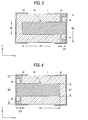
- Fig. 3 is a sectional view taken along the line 3-3 in Fig. 2.
- Fig. 4 is a sectional view taken along the line 4-4 in Fig. 2.
- Fig. 5 is a sectional view taken along the line 5-5 in Fig. 2.
- Fig. 6 is a sectional view taken along the line 6-6 in Fig. 2.
- Fig. 7 is a sectional view taken along the line 7-7 in Fig. 2.
- Fig. 8 is a sectional view showing another embodiment of the semiconductor electronic part according to the present invention.
- Fig. 9 is a sectional view showing another embodiment of the semiconductor electronic part according to the present invention.
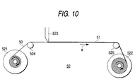
- Fig. 10 is a schematic view for explaining a step for producing the semiconductor electronic part according to the present invention.
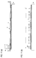
- Figs. 11(a) and 11(b) are schematic views for explaining production steps next to Fig. 10.
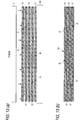
- Fig. 12 is a plan view showing an intermediate product obtained by the production step in Figs. 11(a) and 11(b).
- Figs. 13(a) and 13(b) are schematic views for explaining production steps next to Figs. 11(a) and 11(b).
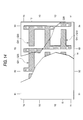
- Fig. 14 is a partly cutaway sectional view showing an intermediate product obtained by the production step in Figs. 13(a) and 13(b).
- Figs. 15(a) and 15(b) are schematic views for explaining a production step next to Figs. 13(a) and 13(b).
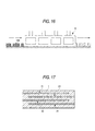
- Fig. 16 is a schematic view for explaining a production step next to Figs. 15(a) and 15(b).
- Fig. 17 is an enlarged sectional view showing an intermediate product obtained by the production step in Fig. 16.
- Figs. 18(a) and 18(b) are schematic views for explaining steps for producing the semiconductor electronic part according to the present invention.
- Figs. 19(a) and 19(b) are schematic views for explaining a production seep next to Figs. 18(a) and 18(b).
- Figs. 20(a), 20(b) and 20(c) are schematic views for explaining production steps next to Figs. 19(a) and 19(b).
- Fig. 1 is a perspective view showing a semiconductor electronic part according to the present invention.
- Fig. 2 is an enlarged sectional view taken along the line 2-2 in Fig. 1.
- Fig. 3 is a sectional view taken along the line 3-3 in Fig. 2.
- Fig. 4 is a sectional view taken along the line 4-4 in Fig. 2.
- Fig. 5 is a sectional view taken along the line 5-5 in Fig. 2.
- An embodiment shown in Figs. 1 to 5 shows a varistor.
- the present invention is not limited thereto but may be applied also to semiconductor electronic parts such as PTC thermistor, NTC thermistor, semiconductor capacitor, etc.
- the semiconductor electronic part shown in the drawings comprises a semiconductor ceramic substrate 1, and internal electrodes 21 to 24.
- the semiconductor ceramic substrate 1 is shaped like a rectangle about 1.0 mm long, about 0.5 mm wide and about 0.5 mm thick.
- the semiconductor ceramic substrate 1 is selected in accordance with the kind of the semiconductor electronic part to be obtained. Because a varistor is shown in this embodiment, it will go well if the semiconductor ceramic substrate 1 is made of voltage-nonlinearity semiconductor ceramics as described above.
- the internal electrodes 21 to 24 are provided inside the semiconductor ceramic substrate 1 so as to be distanced from one another in a thicknesswise direction Z. Each of the internal electrodes 21 and 23 has one end led out to one end edge of the semiconductor ceramic substrate 1 in the lengthwise direction X. Each of the internal electrodes 22 and 24 has the other end led out to the other end edge of the semiconductor ceramic substrate 1 in the lengthwise direction X.
- the internal electrode 21 has cutout regions 31 and 32.
- the internal electrode 22 has cutout regions 33 and 34.
- the internal electrode 23 has cutout regions 35 and 36.
- the internal electrode 24 has cutout regions 37 and 38. In this embodiment, as shown in Figs. 3 and 4, each of the cutout regions 31 to 38 is shaped like a rectangle.
- the cutout regions 31 and 32 are provided at one end edge of the internal electrode 21 in the lengthwise direction X so as to be separated by a distance from each other in a widthwise direction Y.
- the cutout regions 33 and 34 are provided at the other end edge of the internal electrode 22 in the lengthwise direction X so as to be separated by a distance from each other in the widthwise direction Y.
- the cutout regions 35 and 36 are provided at one end edge of the internal electrode 23 in the lengthwise direction X so as to be separated by a distance from each other in the widthwise direction Y.
- the cutout regions 37 and 38 are provided at the other end edge of the internal electrode 24 in the lengthwise direction X so as to be separated by a distance from each other in the widthwise direction Y.
- the internal electrodes 21 to 24 are of the so-called T-type.
- the internal electrodes 21 and 22 will be described below by way of example.
- the internal electrode 21 has a main electrode portion 211, and a pick-up electrode portion 212.
- the pick-up electrode portion 212 is provided on one end side of the main electrode portion 211 in the lengthwise direction X.
- the pick-up electrode portion 212 has a width W2 approximately equal to the width of the semiconductor ceramic substrate 1.
- the main electrode portion 211 has a width W1 smaller than the width W2 of the pick-up electrode portion 212.
- the internal electrode 22 has a main electrode portion 221, and a pick-up electrode portion 222.
- the pick-up electrode portion 222 is provided on the other end side of the main electrode portion 221 in the lengthwise direction X.
- the pick-up electrode portion 222 has a width W2 approximately equal to the width of the semiconductor ceramic substrate 1.
- the main electrode portion 221 has a width Wl smaller than the width W2 of the pick-up electrode portion222.
- each of the internal electrodes 21 to 24 is made of a material that comes into ohmic contact with the aforementioned semiconductor ceramic substrate.
- this embodiment has shown the case where four internal electrodes 21 to 24 are provided, the number of internal electrodes can be changed at option.
- each of the internal electrodes 21 to 24 may be shaped like any figure other than the T-type such as an I-type.
- the semiconductor electronic part shown in this embodiment further comprises terminal electrodes 41 and 42.
- the terminal electrode 41 is provided at one end of the semiconductor ceramic substrate 1 in the lengthwise direction X and connected to end portions of the internal electrodes 21 and 23.
- the terminal electrode 42 is provided at the other end of the semiconductor ceramic substrate 1 in the lengthwise direction X and connected to end portions of the internal electrodes 22 and 24.
- the internal electrodes 21 to 24 are disposed inside the semiconductor ceramic substrate 1, the internal electrodes 21 to 24 are protected by the semiconductor ceramic substrate 1. Hence, a semiconductor electronic part excellent in corrosion resistance, oxidation resistance, impact resistance, etc. is obtained.
- Each of the internal electrodes 21 and 23 has one end led out to one end edge of the semiconductor ceramic substrate 1 in the lengthwise direction X.
- Each of the internal electrodes 22 and 24 has the other end led out to the other end edge of the semiconductor ceramic substrate 1 in the lengthwise direction X.
- the semiconductor electronic part can be used as a chip-like electronic part by provision of the terminal electrodes 41 and 42 in end edges of the semiconductor ceramic substrate 1.
- the one-end sides of the internal electrodes 21 to 24 have cutout regions (31, 32) to (37, 38) respectively.
- the cutout regions (31, 32) to (37, 38) of the internal electrodes 21 to 24 are filled with the semiconductor ceramic substrate 1 as if the internal electrodes 21 to 24 are stitched by the semiconductor ceramic substrate 1 filled in the cutout regions (31, 32) to (37, 38).
- strength of adhesion between the internal electrodes 21 to 24 and the semiconductor ceramic substrate 1 increases.
- troubles such as electrode peeling, chipping, cracking, etc., can be securely prevented.
- the internal electrodes 21 to 24 have the cutout regions (31, 32) to (37, 38) respectively.
- the internal electrodes 21 to 24 have the cutout regions (31, 32) to (37, 38) respectively.
- the cutout regions 31 and 32 are provided at one end edge of the internal electrode 21 in the lengthwise direction X so as to be separated by a distance from each other in the widthwise direction Y.
- the cutout regions 33 and 34 are provided at the other end edge of the internal electrode 22 in the lengthwise direction X so as to be separated by a distance from each other in the widthwise directIon Y.
- the cutout regions 35 and 36 are provided at one end edge of the internal electrode 23 in the lengthwise direction X so as to be separated by a distance from each other in the widthwise direction Y.
- the cutout regions 37 and 38 are provided at one end edge of the internal electrode 24 in the lengthwise direction X so as to be separated by a distance from each other in the widthwise dIrection Y.
- strength of adhesion between the internal electrodes 21 to 24 and the semiconductor ceramic substrate 1 can be increased more greatly compared with the case where one cutout region is provided at one side of the internal electrodes 21 to 24 in the widthwise direction, troubles such as electrode peeling, etc., can be prevented more securely. As a result, the reliability of the semiconductor electronic part is improved more greatly.
- each of the internal electrodes 21 to 24 is shaped like the so-called T-type pattern. In this case, troubles such as electrode peeling, etc., can be prevented securely. Moreover, because of the positions where the cutout regions are provided, troubles such as chipping, cracking, etc. caused by physical stress can be prevented from occurring.
- Sample number #1 shows a conventional product having I-type internal electrodes.
- Sample number #2 shows a conventional product having T-type internal electrodes.
- Sample number #3 shows a semiconductor electronic part according to the present invention having the structure shown in Figs. 1 to 7.
- Table 1 shows the rate of occurrence of defects (chipping, cracking) in external appearance and the rate of occurrence of electrode peeling with respect to the semiconductor electronic parts shown as sample numbers #1 to #3.
- electrode peeling between the internal electrodes and the terminal electrodes is detected in the condition that adhesive double coated tapes are first stuck onto surfaces of the terminal electrodes and then peeled therefrom.
- electrode peeling is observed in 3 in 1000 samples in the semiconductor electronic part shown. as sample number #1 whereas all 1000 samples are good products in the semiconductor electronic part shown as sample number #3.
- chipping is observed in 43 in 1000 samples in the semiconductor electronic part shown as sample number #2 whereas all 1000 samples are good products in the semiconductor electronic part shown as sample number #3.
- cracking is observed in 7 in 10000 samples in the semiconductor electronic part shown as sample number #2 whereas all 10000 samples are good products in the semiconductor electronic part shown as sample number #3, It is apparent from these results that the semiconductor electronic part according to the present invention can prevent troubles such as electrode peeling, chipping, cracking, etc. securely.
- Figs. 8 and 9 are sectional views showing other embodiments of the semiconductor electronic part according to the present invention.
- constituent parts the same as those shown in Figs. 1 to 7 are referenced correspondingly.
- the drawings show the internal electrode 22, they can be applied to the other electrodes 21, 23 and 24.
- each of the cutout regions 31 to 38 is shaped like a half circle.
- the embodiment shown in Fig. 9 is characterized in that the cutout regions 31 to 38 are provided on the inside of an end edge of pick-up electrode portions 212 to 242.
- Each of the embodiments fulfills the same operation and effect as those in the embodiment shown in Figs. 1 to 7.
- a sheet lamination method, a printing method, or the like is known as a method of producing the semiconductor electronic part according to the present invention.
- the producing method will be described below with reference to the drawings, taking the semiconductor electronic part shown in Figs. 1 to 7 as an example.
- Figs. 10 to 17 are schematic views for explaining the sheet lamination method.
- a semiconductor ceramic paste 51 which is prepared by weighing and mixing semiconductor ceramic powder, an organic binder and a solvent in a predetermined proportion, is applied onto a flexible support film 50 by a method such as a doctor blade method, an extrusion method, or the like.
- a ceramic film is obtained.
- the doctor blade method will be described below.
- a coating apparatus 52 includes a feed roller 521, a take-up roller 522, a doctor blade 523, and auxiliary rollers 524 and 525.
- the feed roller 521 and the take-up roller 522 are arranged so as to be separated by a distance from each other.
- the feed roller 521 is wound with one end side of the flexible support film 50, while the take-up roller 522 is wound with the other end side of the flexible support film 50.
- the doctor blade 523 applies the semiconductor ceramic paste 51 onto one surface side of the flexible support film 50 which is running in one direction a .
- the auxiliary rollers 524 and 525 are arranged so as to come into contact with the opposite surface of the flexible support film 50 to the surface of the flexible support film 50 onto which the semiconductor ceramic paste 51 is applied. In this manner, a required number of semiconductor ceramic sheets each having a thickness of from about 0.05 mm to about 0.5 mm are produced.
- a conductor paste 20 is applied onto the semiconductor ceramic sheet 11 to thereby form an electrically conductive coating film set Q.
- the electrically conductive coating film set Q is constituted by a matrix of three rows and three columns of electrically conductive coating films Q11 to Q33, and an electrically conductive coating film Q00. Although the arrangement of the electrically conductive coating films Q11 to Q33 is expressed as a matrix of three rows and three columns, the number of rows and the number of columns can be changed at option.
- the electrically conductive coating film Q00 plays the role of a marker at the time of cutting thereafter.
- a screen printing method using a screen 61 and a squeegee 62 as shown in Fig. 11 (a) is suitable for a method of applying the conductor paste 20.
- the reference numeral 60 designates a support table on which the semiconductor ceramic sheet 11 is mounted.
- the semiconductor ceramic sheets 11 to 15 obtained in the aforementioned steps are oiled up as shown in Fig. 13(a) .
- the semiconductor ceramic sheets 11 to 15 are hot-pressed to thereby obtain a green sheet 10 made from the semiconductor ceramic sheets 11 to 15.
- the temperature and pressure for hot-pressing are preferably in a range of from 40 to 120 °C and in a range of from about 50 X 9.8 X 10 4 Pa to about 1000 X 9.8 X 10 4 Pa, respectively.
- the green sheet 10 is divided individually in the X and Y directions see Fig. 14) in accordance with the arrangement of the electrically conductive coating films Q11 to Q33 to thereby obtain green chips.
- the green chips 100 obtained thus are subjected to a binder removing step as shown in Fig. 16, so that a binder contained in each green chip 100 is removed by heating.
- the green chips 100 are further kept in the temperature condition of about 1000 °C for about 10 minutes to thereby fire the green chips 100.
- the reference numeral 8 designates a firing furnace.
- Figs. 18(a) to 20(c) are schematic views. for explaining a printing method.
- constituent parts the same as those shown in Figs. 10 to 17 are referenced correspondingly.
- a semiconductor ceramic paste 51 onto a support table 60 is repeated by a required number of times by use of a screen 61 and a squeegee 62.
- a semiconductor ceramic sheet 11 is obtained as shown in Fig. 18(b).
- a conductor paste 20 is applied onto the semiconductor ceramic sheet 11 by use of the screen 61 and the squeegee 62.
- a conductor paste 20 is applied onto the semiconductor ceramic sheet 11 by use of the screen 61 and the squeegee 62.
- Fig. 19(b) an arrangement of electrically conductive coating films Q11 to Q33 and Q00 is formed on the semiconductor ceramic sheet 11.
- the semiconductor ceramic paste 51 and the conductor paste 20 are alternately applied by use of the screen 61 and the squeegee 62 to thereby obtain a green sheet 10 shown in Fig. 20(c).
- the green sheet 10 obtained thus is subjected to the individually dividing step, the binder removing step and the firing step and then the terminal electrodes 41 and 42 are added to the green sheet, in the same manner as that in the sheet lamination method.
- the semiconductor electronic part which is a final product is obtained.
Landscapes
- Engineering & Computer Science (AREA)
- Power Engineering (AREA)
- Microelectronics & Electronic Packaging (AREA)
- Ceramic Engineering (AREA)
- Chemical & Material Sciences (AREA)
- Manufacturing & Machinery (AREA)
- Inorganic Chemistry (AREA)
- Physics & Mathematics (AREA)
- Electromagnetism (AREA)
- Thermistors And Varistors (AREA)
- Ceramic Capacitors (AREA)
- Led Device Packages (AREA)
Applications Claiming Priority (2)
| Application Number | Priority Date | Filing Date | Title |
|---|---|---|---|
| JP34549399A JP2001167908A (ja) | 1999-12-03 | 1999-12-03 | 半導体電子部品 |
| JP34549399 | 1999-12-03 |
Publications (2)
| Publication Number | Publication Date |
|---|---|
| EP1107265A2 true EP1107265A2 (de) | 2001-06-13 |
| EP1107265A3 EP1107265A3 (de) | 2006-03-29 |
Family
ID=18376965
Family Applications (1)
| Application Number | Title | Priority Date | Filing Date |
|---|---|---|---|
| EP00126322A Withdrawn EP1107265A3 (de) | 1999-12-03 | 2000-12-01 | Elektronischer Halbleiterteil |
Country Status (4)
| Country | Link |
|---|---|
| US (1) | US6385034B2 (de) |
| EP (1) | EP1107265A3 (de) |
| JP (1) | JP2001167908A (de) |
| NO (1) | NO20006133L (de) |
Cited By (1)
| Publication number | Priority date | Publication date | Assignee | Title |
|---|---|---|---|---|
| WO2007084658A1 (en) * | 2006-01-18 | 2007-07-26 | Kemet Electronics Corporation | Low inductance capacitor |
Families Citing this family (29)
| Publication number | Priority date | Publication date | Assignee | Title |
|---|---|---|---|---|
| TW412755B (en) * | 1998-02-10 | 2000-11-21 | Murata Manufacturing Co | Resistor elements and methods of producing same |
| JP2003051423A (ja) * | 2001-08-03 | 2003-02-21 | Tdk Corp | 電子部品 |
| US20070007621A1 (en) * | 2005-03-30 | 2007-01-11 | Yamaha Corporation | Fuse breakdown method adapted to semiconductor device |
| WO2007020757A1 (ja) * | 2005-08-19 | 2007-02-22 | Murata Manufacturing Co., Ltd. | 積層セラミックコンデンサ |
| JP2007134555A (ja) * | 2005-11-11 | 2007-05-31 | Matsushita Electric Ind Co Ltd | 電子部品及びその製造方法 |
| JP4600309B2 (ja) * | 2006-02-13 | 2010-12-15 | Tdk株式会社 | バリスタ及び発光装置 |
| TWI427646B (zh) | 2006-04-14 | 2014-02-21 | Bourns Inc | 具表面可裝設配置之傳導聚合物電子裝置及其製造方法 |
| US20080057619A1 (en) * | 2006-08-30 | 2008-03-06 | Honeywell International Inc. | Microcontainer for Hermetically Encapsulating Reactive Materials |
| JP4378370B2 (ja) * | 2006-09-25 | 2009-12-02 | Tdk株式会社 | 積層コンデンサ |
| JP4378371B2 (ja) * | 2006-09-29 | 2009-12-02 | Tdk株式会社 | 積層コンデンサ |
| JP4385385B2 (ja) * | 2006-12-14 | 2009-12-16 | Tdk株式会社 | 積層コンデンサ |
| WO2009001842A1 (ja) * | 2007-06-27 | 2008-12-31 | Murata Manufacturing Co., Ltd. | 積層セラミック電子部品及びその実装構造 |
| JP4428446B2 (ja) * | 2007-12-28 | 2010-03-10 | Tdk株式会社 | 積層コンデンサ |
| DE102008024479A1 (de) * | 2008-05-21 | 2009-12-03 | Epcos Ag | Elektrische Bauelementanordnung |
| US8446705B2 (en) * | 2008-08-18 | 2013-05-21 | Avx Corporation | Ultra broadband capacitor |
| JP2010073759A (ja) * | 2008-09-16 | 2010-04-02 | Tdk Corp | 積層型チップバリスタ及び電子部品 |
| JP5472667B2 (ja) * | 2011-02-04 | 2014-04-16 | 株式会社村田製作所 | バリスタ機能付き積層型半導体セラミックコンデンサとその製造方法 |
| DE102011109007A1 (de) * | 2011-07-29 | 2013-01-31 | Epcos Ag | Verfahren zum Herstellen eines elektrischen Bauelements und elektrisches Bauelement |
| KR102126420B1 (ko) * | 2013-06-10 | 2020-06-24 | 삼성전기주식회사 | 적층 세라믹 커패시터 및 적층 세라믹 커패시터 실장 기판 |
| US20150146340A1 (en) * | 2013-11-26 | 2015-05-28 | Qualcomm Incorporated | Multilayer ceramic capacitor including at least one slot |
| JP2014222783A (ja) * | 2014-08-13 | 2014-11-27 | 株式会社村田製作所 | 積層コンデンサ及び積層コンデンサの実装構造体 |
| JP2014220528A (ja) * | 2014-08-13 | 2014-11-20 | 株式会社村田製作所 | 積層コンデンサ |
| KR102236098B1 (ko) * | 2015-02-16 | 2021-04-05 | 삼성전기주식회사 | 적층 세라믹 전자 부품 |
| MY192095A (en) * | 2016-03-07 | 2022-07-27 | Kyocera Avx Components Corp | Multi-layer electronic device |
| AU2018374354A1 (en) * | 2017-12-01 | 2020-06-11 | KYOCERA AVX Components Corporation | Low aspect ratio varistor |
| JP7200499B2 (ja) * | 2018-04-26 | 2023-01-10 | Tdk株式会社 | 積層コイル部品 |
| KR20200040429A (ko) * | 2018-10-10 | 2020-04-20 | 삼성전기주식회사 | 적층 세라믹 전자부품 |
| DE102019105116A1 (de) * | 2019-02-28 | 2020-09-03 | Tdk Electronics Ag | Bauelement |
| KR102762876B1 (ko) * | 2019-09-17 | 2025-02-07 | 삼성전기주식회사 | 적층형 전자 부품 |
Family Cites Families (14)
| Publication number | Priority date | Publication date | Assignee | Title |
|---|---|---|---|---|
| US3740624A (en) * | 1972-06-21 | 1973-06-19 | Sprague Electric Co | Monolithic capacitor having corner internal electrode terminations |
| US4731697A (en) * | 1987-05-05 | 1988-03-15 | Avx Corporation | Arc resistant trimable ceramic capacitor |
| JPH01312817A (ja) * | 1988-06-09 | 1989-12-18 | Murata Mfg Co Ltd | 積層セラミックコンデンサの製造方法 |
| JPH03178107A (ja) * | 1989-12-06 | 1991-08-02 | Matsushita Electric Ind Co Ltd | 積層セラミックコンデンサ |
| JPH0590064A (ja) * | 1991-09-26 | 1993-04-09 | Nec Kansai Ltd | 積層セラミツクコンデンサ及びその製造方法 |
| JPH0590062A (ja) * | 1991-09-26 | 1993-04-09 | Matsushita Electric Ind Co Ltd | 積層型粒界絶縁型半導体セラミツクコンデンサ |
| JPH06208903A (ja) * | 1993-01-11 | 1994-07-26 | Murata Mfg Co Ltd | 正の抵抗温度特性を有する積層型半導体磁器 |
| JPH0897071A (ja) * | 1994-09-29 | 1996-04-12 | Kyocera Corp | 積層型磁器コンデンサ |
| US6153069A (en) * | 1995-02-09 | 2000-11-28 | Tall Oak Ventures | Apparatus for amperometric Diagnostic analysis |
| JPH09260198A (ja) * | 1996-03-25 | 1997-10-03 | Taiyo Yuden Co Ltd | 積層コンデンサ |
| US5872695A (en) * | 1997-02-26 | 1999-02-16 | International Business Machines Corporation | Integrated electronic components having conductive filled through holes |
| JPH10275736A (ja) * | 1997-03-28 | 1998-10-13 | Tdk Corp | 積層基板の切断位置の良否判定方法と積層セラミック電子部品 |
| JP3684290B2 (ja) * | 1997-06-16 | 2005-08-17 | 太陽誘電株式会社 | 積層電子部品とその製造方法 |
| US5880925A (en) * | 1997-06-27 | 1999-03-09 | Avx Corporation | Surface mount multilayer capacitor |
-
1999
- 1999-12-03 JP JP34549399A patent/JP2001167908A/ja active Pending
-
2000
- 2000-12-01 EP EP00126322A patent/EP1107265A3/de not_active Withdrawn
- 2000-12-01 US US09/726,512 patent/US6385034B2/en not_active Expired - Fee Related
- 2000-12-01 NO NO20006133A patent/NO20006133L/no not_active Application Discontinuation
Cited By (1)
| Publication number | Priority date | Publication date | Assignee | Title |
|---|---|---|---|---|
| WO2007084658A1 (en) * | 2006-01-18 | 2007-07-26 | Kemet Electronics Corporation | Low inductance capacitor |
Also Published As
| Publication number | Publication date |
|---|---|
| NO20006133D0 (no) | 2000-12-01 |
| EP1107265A3 (de) | 2006-03-29 |
| JP2001167908A (ja) | 2001-06-22 |
| US6385034B2 (en) | 2002-05-07 |
| NO20006133L (no) | 2001-06-05 |
| US20010002873A1 (en) | 2001-06-07 |
Similar Documents
| Publication | Publication Date | Title |
|---|---|---|
| US6385034B2 (en) | Semiconductor electronic part | |
| US6232867B1 (en) | Method of fabricating monolithic varistor | |
| US5075665A (en) | Laminated varistor | |
| EP1347476B1 (de) | Keramisches elektronikbauteil und dessen herstellungsverfahren | |
| KR101055161B1 (ko) | 세라믹 소자 | |
| US4792781A (en) | Chip-type resistor | |
| US5963416A (en) | Electronic device with outer electrodes and a circuit module having the electronic device | |
| US6316726B1 (en) | Surface mount electronic component having electrodes suppressing the occurrence of migration | |
| GB2224392A (en) | Conducive ceramic terminations of capacitor | |
| US20040140595A1 (en) | Method for manufacturing multilayer ceramic electronic component | |
| KR20190058239A (ko) | 적층 세라믹 커패시터 및 그 제조방법 | |
| EP0858085B1 (de) | Chip-Vielschichtlaminat-Varistor und Verfahren zu seiner Herstellung | |
| KR20200062354A (ko) | 향상된 연결성을 갖는 다층 전자 디바이스 및 다층 전자 디바이스의 제조 방법 | |
| JPH03173402A (ja) | チップバリスタ | |
| US7372357B2 (en) | Varistor body and varistor | |
| JPH056805A (ja) | チツプ型バリスタ | |
| US4756928A (en) | Method of forming electrodes of an electronic component of chip type for connecting to the external | |
| KR100693119B1 (ko) | 세라믹 부품 요소, 세라믹 부품 및 그 제조 방법 | |
| US20070229209A1 (en) | Varistor body and varistor | |
| US20250201477A1 (en) | Multilayer ceramic electronic device and manufacturing method of the same | |
| JPH04154104A (ja) | 積層セラミックコンデンサ | |
| US12354804B2 (en) | Multilayer ceramic electronic device | |
| JP2000068109A (ja) | チップ型サーミスタとその製造方法 | |
| TWI761589B (zh) | 陶瓷電子零件及其製造方法 | |
| EP0390944B1 (de) | Herstellungsprozess für ein keramisches mehrschichtiges Substrat |
Legal Events
| Date | Code | Title | Description |
|---|---|---|---|
| PUAI | Public reference made under article 153(3) epc to a published international application that has entered the european phase |
Free format text: ORIGINAL CODE: 0009012 |
|
| AK | Designated contracting states |
Kind code of ref document: A2 Designated state(s): AT BE CH CY DE DK ES FI FR GB GR IE IT LI LU MC NL PT SE TR |
|
| AX | Request for extension of the european patent |
Free format text: AL;LT;LV;MK;RO;SI |
|
| PUAL | Search report despatched |
Free format text: ORIGINAL CODE: 0009013 |
|
| AK | Designated contracting states |
Kind code of ref document: A3 Designated state(s): AT BE CH CY DE DK ES FI FR GB GR IE IT LI LU MC NL PT SE TR |
|
| AX | Request for extension of the european patent |
Extension state: AL LT LV MK RO SI |
|
| AKX | Designation fees paid | ||
| STAA | Information on the status of an ep patent application or granted ep patent |
Free format text: STATUS: THE APPLICATION IS DEEMED TO BE WITHDRAWN |
|
| 18D | Application deemed to be withdrawn |
Effective date: 20060930 |
|
| REG | Reference to a national code |
Ref country code: DE Ref legal event code: 8566 |