EP1102182A2 - Verfahren zum automatischen Entwurf eines Layouts für LSI, Maskensatz und nach dem Verfahren hergestellte integrierte Halbleiterschaltung, und Aufzeichnungsmedium zur Speicherung das Programms - Google Patents
Verfahren zum automatischen Entwurf eines Layouts für LSI, Maskensatz und nach dem Verfahren hergestellte integrierte Halbleiterschaltung, und Aufzeichnungsmedium zur Speicherung das Programms Download PDFInfo
- Publication number
- EP1102182A2 EP1102182A2 EP00124343A EP00124343A EP1102182A2 EP 1102182 A2 EP1102182 A2 EP 1102182A2 EP 00124343 A EP00124343 A EP 00124343A EP 00124343 A EP00124343 A EP 00124343A EP 1102182 A2 EP1102182 A2 EP 1102182A2
- Authority
- EP
- European Patent Office
- Prior art keywords
- line
- lines
- clock
- oblique
- chip
- Prior art date
- Legal status (The legal status is an assumption and is not a legal conclusion. Google has not performed a legal analysis and makes no representation as to the accuracy of the status listed.)
- Withdrawn
Links
Images







Classifications
-
- H—ELECTRICITY
- H10—SEMICONDUCTOR DEVICES; ELECTRIC SOLID-STATE DEVICES NOT OTHERWISE PROVIDED FOR
- H10D—INORGANIC ELECTRIC SEMICONDUCTOR DEVICES
- H10D84/00—Integrated devices formed in or on semiconductor substrates that comprise only semiconducting layers, e.g. on Si wafers or on GaAs-on-Si wafers
-
- H—ELECTRICITY
- H10—SEMICONDUCTOR DEVICES; ELECTRIC SOLID-STATE DEVICES NOT OTHERWISE PROVIDED FOR
- H10W—GENERIC PACKAGES, INTERCONNECTIONS, CONNECTORS OR OTHER CONSTRUCTIONAL DETAILS OF DEVICES COVERED BY CLASS H10
- H10W20/00—Interconnections in chips, wafers or substrates
- H10W20/40—Interconnections external to wafers or substrates, e.g. back-end-of-line [BEOL] metallisations or vias connecting to gate electrodes
- H10W20/41—Interconnections external to wafers or substrates, e.g. back-end-of-line [BEOL] metallisations or vias connecting to gate electrodes characterised by their conductive parts
- H10W20/43—Layouts of interconnections
-
- G—PHYSICS
- G06—COMPUTING OR CALCULATING; COUNTING
- G06F—ELECTRIC DIGITAL DATA PROCESSING
- G06F1/00—Details not covered by groups G06F3/00 - G06F13/00 and G06F21/00
- G06F1/04—Generating or distributing clock signals or signals derived directly therefrom
- G06F1/10—Distribution of clock signals, e.g. skew
-
- G—PHYSICS
- G06—COMPUTING OR CALCULATING; COUNTING
- G06F—ELECTRIC DIGITAL DATA PROCESSING
- G06F30/00—Computer-aided design [CAD]
- G06F30/30—Circuit design
- G06F30/39—Circuit design at the physical level
- G06F30/394—Routing
Definitions
- This invention relates to a technique of automatic layout design applied to CAD for placement and routing.
- the invention also relates to a mask set and a semiconductor integrated circuit manufactured by the automatic layout design technique, and to a recording medium storing the automatic layout program.
- horizontal and vertical lines In designing interconnection of basic horizontal and vertical lines in the orthogonal coordinate system on CAD, horizontal and vertical lines often terminate at an intersection of two or more orthogonal lines. If the horizontal lines and the vertical lines are formed in different layers in an actual semiconductor device, a via hole must be formed at the terminal portions of the metal lines to connect the horizontal and vertical lines three-dimensionally. Accordingly, a connection pattern corresponds to the via hole must be defined at a terminal of horizontal and vertical lines on CAD.
- terminal processing is carried out to extend the ends of the orthogonal lines by W/2.
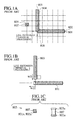
- FIG. 1 shows an example of terminal processing of the basic orthogonal lines of the minimum width.
- a horizontal line 801 and a vertical line 803 meet each other at a terminal.
- a CAD system only the intersection point at which the center lines 802 and 804 of the respective lines cross each other is recognized as an intersection 808.
- the CAD does not recognize the overlap of two orthogonal lines at all.
- connection pattern 805 (Fig. 1C) at the intersection of the two orthogonal lines 801 and 803.
- the connection pattern 805 consists of a bottom metal 801a, which is a part of the end portion of the line 801, a top metal 803a, which is a part of the end portion of the line 803, and an opening 807 (hereinafter, referred to as a "cut") for connecting the top and bottom metals 803a and 801a.
- the CAD recognizes two lines crossing each other, and accordingly, it is possible to define the connection pattern 805 at the intersection recognized by the CAD. However, if the two lines terminate in the state shown in FIG. lA, the overlapped area between the horizontal line 801 and the vertical line 803 is very small. If a via hole is formed in an actual integrated circuit based on the layout shown in Fig. 1A, the lines of the upper and lower layers can not be reliably connected.
- connection pattern 805 is placed on the overlapped area.
- FIG. 1C illustrates a connection pattern 805 and a side view of a via hole formed in an actual integrated circuit.
- the connection pattern 805 is square because it is placed at the intersection of two basic orthogonal lines.
- FIG. 2 illustrates another conventional example of terminal processing of two orthogonal lines.
- two wider orthogonal lines meet each other and terminate at the junction.
- the wide lines are treated as special lines in CAD
- both of the horizontal line 811 and the vertical line 811 are extended by W/2, so that the end portions of these lines completely overlap each other, like in Fig. 1. Because the overlapped area is large, a connection pattern 805 having a plurality of cuts 817 is placed in the overlapped area.
- the inventors of the present invention have proposed in Japanese Patent Application Nos. 10-176285 and 11-175930 a technique for greatly reducing a line resistance of oblique lines itself. This is achieved by setting the width and film thickness of the oblique line to ⁇ 2 times as large as those of the basic orthogonal lines.
- the optimal shapes of via holes for connecting metal lines of different layers are also proposed in order to reliably guarantee the cross-sectional area of the cut.
- the inventors also proposed a tree-type clock supply path comprised of a combination of oblique lines and the basic orthogonal lines.
- LSI large scaled integrated circuit
- the CSD can generate a circuit layout using oblique lines with less data amount.
- an automatic layout method used to, for example, CAD is provided.
- a first line having a first width is generated in a prescribed direction.
- a second line having a second width is generated so that the second line extends at an oblique angle with respect to the first line and terminates at an end portion of the first line with an overlapped area between the first and second lines.
- one or more VIA patterns are placed in the overlapped area so that one of them is located at an intersection of the longitudinal center lines of the first and second lines.
- the method further comprises the step of detecting if there are any unnecessary areas projecting from the overlapped area, and deleting the unnecessary areas if there are any.
- the wiring resources i.e., effective areas on a semiconductor substrate
- first and second lines have the minimum line width of the lithography technique
- a single connection pattern is set at the intersection. If neither the first or second line has the minimum width, then, multiple connection patterns are set inside the overlapped area. In the latter case, the data processing time and amount can be reduced because only the same connection pattern is repeatedly generated.
- connection pattern is a combination of parallelograms (including squares and rectangles). At least a pair of parallel sides of the parallelogram is parallel to either the first or second line. In addition, the first and second lines can be reliably connected in an actual device manufactured from the layout.
- connection pattern consists of, for example, a first parallelogram, which is the end portion of the first line, a second parallelogram, which is the end portion of the second line, and a cut square placed inside the overlapped area of the first and second parallelograms.
- a parallelogram includes a square and a rectangle.
- An assembled VIA pattern may be placed on the overlapped area if the overlapped area is relatively large.
- the assembled VIA pattern consists of a first parallelogram, which is the end portion of the first line, a second parallelogram, which is the end portion of the second line, and a set of cut squares in the overlapped area of the first and second parallelograms. One of the cut squares is located at the intersection of the first and second lines.
- the first and second lines represent, for example, wiring patterns located in different layers of a semiconductor device. Alternatively, the first and second lines represent wiring patterns located in a same layer of a semiconductor device.
- an exposure mask set used to manufacture a semiconductor device comprising at least a first mask having basic orthogonal line patterns, a second mask having aperture patterns for via holes, and a third mask having oblique line patterns.
- the aperture patterns of the second mask are aligned to the end portions of the orthogonal line patterns of the first mask.
- the oblique line patterns of the third mask extend at an oblique angle with respect to the orthogonal line patterns of the fist mask.
- the end portions of the oblique line patterns are aligned to both the end portions of the orthogonal line patterns of the first mask and the aperture patterns of the second mask.
- a multi-layered wiring structure using oblique lines can be manufactured, in which upper-layer lines and lower-layer lines are reliably connected, while preventing waste of the wiring resources at each layer.
- a semiconductor integrated circuit having an oblique line structure which is manufactured using the above-mentioned mask set, is provided.
- One example of such integrated circuit comprises a first wiring layer including orthogonal line patterns with a first line width, an insulating layer placed on the first wiring layer, and a second wiring layer placed on the insulating layer and including oblique line patterns with a second line width.
- Via contacts penetrate through the insulating layer in order to connect the orthogonal line patterns of the first layer and the oblique line patterns of the second layers.
- the end portions of the oblique line patterns are positioned directly above the end portions of the orthogonal line patterns of the first wiring layer.
- the via contact connects the orthogonal line pattern and the oblique line pattern at the end portions of these line patters.
- the horizontal cross-section of the via contact is square, and is completely inside the end portion of a narrower line pattern.
- the end portion of an orthogonal line may be connected to the end portion of an oblique line through one or more via contacts.
- one of the via contacts is located at the intersection of the center lines of the orthogonal line and the oblique line.
- oblique-line integrated circuit comprises a PLL (phase-locked loop circuit) located at a corner of a chip, a main clock supply line extending from the PLL toward the center of the chip.
- the main clock supply line extends obliquely with respect to the orthogonal coordinate axes of the chip, and a clock tree extends from the end of the main clock supply line.
- the clock tree consists of clock lines that symmetrically branch off in oblique directions with respect to the basic orthogonal coordinate axes.
- This configuration allows the load capacitance to be balanced in the chip, and allows the PLL to supply clocks accurately at a high speed.
- the clock tree is comprised of multiple layers, and clock lines located in a same layer extends in a same oblique direction. This arrangement can reduce variations in signal transfer.
- Still another example of the oblique-line integrated circuit comprises a PLL located at a corner of a chip, and a clock mesh covering the entire area of the chip.
- the clock mesh consists of oblique lines extending at an oblique angle with respect to the orthogonal coordinate axes of the chip.
- the clock mesh is formed in a same layer, thereby allowing a clock to be supplied to elements in the chip quickly.
- Still another example of the oblique-line integrated circuit comprises a clock mesh consisting of oblique lines extending at an oblique angle with respect to the orthogonal coordinate axes of a chip, and a root driver for driving the entire clock mesh.
- a main clock supply line extends from the root driver, and multiple sub-drivers are connected to the main clock supply line. The sub-drivers drive the oblique lines independently. This arrangement can reduce a delay and a skew in the circuit.
- an LSI comprises a main PLL positioned near the periphery of a chip of the integrated circuit, a base-clock supply line extending from the main phase-locked loop, and a plurality of random blocks arranged in the chip.
- the base-clock supply line supplies a base clock (or a global clock) at a lower frequency.
- Each of the random blocks has a clock driver cell connected to the base-clock supply line, and a clock tree consisting of oblique lines.
- the clock driver cell converts the base clock into a higher frequency clock, and supplies the higher frequency clock to elements inside the associated block via the clock tree.
- the base-clock supply line extends across the chip in a direction parallel to an orthogonal coordinate axis of the chip, or alternatively, it extends across the chip in a direction oblique with respect to the orthogonal coordinate axes of the chip.
- the LSI comprises a main PLL positioned near the periphery of a chip, a base-clock supply line extending from the main PLL, and a plurality of random blocks having oblique clock meshes.
- the base-clock supply line supplies base clocks at a relatively low frequency.
- Each random block has a clock driver cell connected to the base-clock supply line. The clock driver cell converts the base clock into a higher frequency clock and supplies the higher frequency clock to elements inside the block via the oblique clock mesh.
- clock mesh consisting of oblique lines
- high-frequency clocks can be supplied to various elements scattered in the block at the shortest distance with little delay.
- a Method for manufacturing a semiconductor integrated circuit is provided.
- first metal lines extending in a prescribed direction are formed on a semiconductor substrate.
- an insulating layer is formed over the first metal lines and the semiconductor substrate.
- via holes are formed in the insulating layer.
- the via-holes penetrate through the insulating layer and reach the end portions of the first metal lines.
- the bottom of each via hole is completely inside the associated first metal line.
- the via-holes are filled with a conductive material to form contacts.
- second metal lines extending at an oblique angle with respect to the first metal lines are formed on the insulating layer, so that the end portions of the second metal lines completely cover the top faces of the contacts.
- a storage medium storing an automatic layout program is provided.
- This program is used to operate a CAD for designing, for example, an LSI.
- the program comprises the following steps:
- the storage medium includes, but are not limited to, external memory, a semiconductor memory, a magnetic disc, optical disc, an optomagnetic disc, a magnetic tape, and so on. Floppy diskette, CD-ROM, MO discs are also included in the storage medium.
- a terminal area or an overlapped area
- the most suitable connection pattern is selected and placed at the terminal area, so that the oblique line and the orthogonal line are reliably connected in an actual device or circuit.
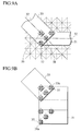
- FIG. 3 is a terminal layout of two lines produced on a CAD based on an automatic design method according to a first embodiment.
- a horizontal line 1 with the minimal line width of lithography is produced.
- an oblique line 13 whose line width is ⁇ 2 times as large as horizontal line 1 is produced.
- the ⁇ 2-time width of the oblique line is the minimum width of the oblique line in this invention.
- the oblique line 13 extends at an oblique angle (135 degrees in the illustrative embodiment) with respect to the horizontal line 11.
- the oblique line 13 terminates at the end portion of the horizontal line 11.
- the oblique line 13 may extend at an angle of 45 degrees or other angles with respect to the horizontal line 11.
- Such layouts are also included in the scope of the invention.
- connection pattern 15A for connecting the horizontal line 11 and the oblique line 13 is produced at an intersection 18 of the center line 12 of the horizontal line 11 and the center line 14 of the oblique line 13.
- the connection pattern is generally called a "via", which corresponds to a via-contact in the actual semiconductor integrated circuit device.
- the connection pattern 15A has a cut pattern 17, which is the innermost cross-marked square in Fig. 3.
- the cut pattern 17 represents a via hole, in which a conductive material, such as doped poly-silicon, tungsten (W), molybdenum (Mo), titanium (Ti), or their silicide (WSi 2 , MoSi 2 , TiSi 2 ), is filled in order to connect the horizontal line 11 and the oblique line 13 in the actual semiconductor device.
- a cut pattern produced in the layout is merely called "cut”.
- a significant feature of the automatic layout design shown in Fig. 3 is that the horizontal line 11 and the oblique line 13 sufficiently overlap each other at their terminal ends, and consequently, the projection 16 sticking out of the edge of the line is extremely small.
- projection due to the horizontal line 11 is zero, and the projection due to the oblique line 13 is only a small triangular region 16. Since the projection 16 is so small that it does not adversely affect the coupling capacitance between adjacent lines or the capacitance between the wiring pattern and the substrate.
- the wiring resource in the layer of the oblique lines is efficiently used minimizing wasted region in that layer.
- connection pattern 15A is generated in square shape only. Generating figures using only those lines crossing at right angle for the same layer (i.e., the same mask) requires relatively small amount of data, as compared with producing figures using non-orthogonal lines, such as a parallelogram or a diamond shape.
- Fig. 4 illustrates the configuration of the connection pattern 15A.
- Fig. 4A shows the horizontal line 11 and oblique line 13 in an exploded manner for convenience of illustration.
- Fig. 4B and Fig. 4C are top and sectional views defining the shape of the connection pattern 15A on EDA (placement and routing tool).
- the connection pattern 15A is comprised of a top metal 13a, a bottom metal lla, and a cut 17 for connecting the top and bottom metals.
- the top metal 13a is a part of the end portion of the oblique line 13, and the bottom metal lla is a part of the end portion of the horizontal line 11.
- both metals have square shapes whose sides are consistent with the sides of the lines 11 and 13.
- the shapes of the top and bottom metals may be rectangular, instead of square.
- a fringe may be provided to the top and/or bottom metals so that the metals expand beyond the are contour of the oblique and/or horizontal lines 13 and 11. In this case, the end portions of the oblique line 13 and the horizontal line 11 are expanded outward in advance.
- a cut 17 is defined inside the overlapped area between the top metal 13a and the bottom metal lla.
- Fig. 4B is a top view of the connection pattern 15A.
- the square drawn by the dashed line represents the bottom metal lla.
- a connection pattern that consists of only squares of the minimum widths is called a standard via in this specification.
- the connection pattern 15A shown in Fig. 4 is the standard via.
- Fig. 4C is a sectional shape of the connection pattern 15A on EDA.
- the cut 17 is completely covered with the top metal 13a.
- the automatic design method illustrated in Fig. 3 has advantages of not requiring deletion of unnecessary area, which results in reduced amount of data processing.
- a connection pattern can be generated by a combination of squares only, which also allows the amount of data processing to be reduced.
- the mask data for each layer contain only orthogonal line data. In this way, the overall computation of CAD is reduced, and consequently, the layout processing speed is improved. In addition, this arrangement facilitates verification of the design rule.
- An actual semiconductor device manufacture by this method has a reliable performance because the via-holes filled with a metal are completely covered with the top metals, and the metal in the via-holes is prevented from melting out of the holes.
- the oblique line structure can improve the signal transfer speed to a target element (for example, a flip-flop).
- Figs. 5 and 6 illustrate another example of automatic layout design for oblique line patterns with the minimum line width.
- a horizontal line 11 of the minimum width is first produced.
- the end of the horizontal line 11 is extended by W/2 from the intersection 18 as in Fig. 3.
- an oblique line 13, which is ⁇ 2 times as wide as the horizontal line 11, is produced.
- the end of the oblique line 13 is extended from the intersection 18 by an amount W so that the end portion of the oblique line 13 sufficiently overlaps the horizontal line 11.
- a connection pattern 15B of a parallelogram is defined at the intersection 18 of the center line 12 of the horizontal line 11 and the center line 14 of the oblique line 13.
- Fig. 5B illustrates a layout after deletion.
- the deletion of a part of the line requires an increased amount of programming data in CAD.
- deletion of the projection 16 can remove the problems of adverse influence to the coupling capacitance and waste of the wiring resources.
- the oblique line 13 completely overlaps the horizontal line 11 at the parallelogramic area. This means that these two lines are securely connected to each other in an actual device.
- connection pattern 15B illustrates the connection pattern 15B more clearly in a top view and a sectional view.
- the connection pattern 15B consists of a parallelogramic top metal 13b, a square bottom metal 11b, and a cut 17.
- the top metal 13b is a part of the end portion of the oblique line 13.
- the bottom metal 11b is a part of the end portion of the horizontal line 11.
- the cut 17 is positioned inside the overlapped area between the top metal 13b and the bottom metal 11b.
- connection pattern 15B In order to define the connection pattern 15B on CAD, it is better to generate a parallelogramic connection pattern on the program in advance and to store it in, for example, a library. Producing the bottom metal 11b and the cut 17 for the connection pattern 15B is easy because of their square shapes. On the other hand, generating the parallelogramic top metal 13b on the layout requires a great amount of computation. Accordingly, it is much efficient to produce the parallelogramic connection pattern 15B on the program in advance, and store it in the database. The connection pattern 15B is read out of the database when it is required. This method can facilitate the terminal treatment of oblique line patterns. By using the connection pattern 15B, the top metal 13a securely covers the cut 17, and prevents the metals in the lower layers from melting during the actual process at a high temperature.
- a parallelogram For producing and storing a connection pattern of a parallelogram, a parallelogram may be defined as it is, or alternatively, it may be defined by dividing into triangles and rectangles in accordance with the actual process.
- the horizontal line 11 is in a lower layer and the oblique line 13 is in an upper layer, the location of these lines may be reversed. Such a configuration can also achieve the same effect and advantages of the invention.
- the horizontal line 11 may be a vertical line, as long as it is parallel to the orthogonal coordinate axes of the layout.
- the present invention is not limited to the two-layer structure, but is also applicable to multi-layered structure including three or more layers and three-dimensional interconnections.
- Fig. 7 illustrates a terminal layout of an oblique line and a horizontal line whose line widths are greatly different.
- the oblique line 23 is much wider than the horizontal line 21 that has the minimum width of lithography.
- a horizontal line 21 with the minimum width is generated.
- an oblique line 23 is generated at an oblique angle (135 degrees in Fig. 7) with respect to the horizontal line 21, so that the end portion of the oblique line 23 overlaps the end portion of the horizontal line 21.
- a connection pattern 25A is placed at the intersection of the center line 22 of the horizontal line 21 and the center line 24 of the oblique line 23.
- the crossed square inside the connection pattern 25A is a cut 27 for connecting the horizontal line 21 and the oblique line 23.
- connection pattern 25A used in this layout is a standard via. This pattern is the same as the connection pattern 15A of the first embodiment shown in Figs. 4B and 4C.
- the connection pattern 25A includes a square 23a located at the middle of the end of the oblique line 23, which represents an top metal 23a, and an end square 21a of the horizontal line 21 indicated by dashed line, which represents a bottom metal 21a.
- CAD generally recognizes a crossing point, at which the longitudinal center lines of two metal lines cross each other, as an intersection of the metal lines, regardless of the line width, in order to handle graphic data efficiently. If the oblique line 23 is moved upward a little more, no intersection will exist in the overlapped area, and a connection pattern cannot be defined. Accordingly, the location of the oblique line 23 shown in Fig. 7 is the upper limit. With this layout, the VIA pattern 25A (including the cut and the upper and lower metals) is completely included in the wide oblique line 23, and there is no need to delete any portions on the layout, while achieving reliable connection.
- FIG. 8 illustrates another example of a terminal layout of a wide oblique line, in which an unnecessary projection 26 is to be deleted after the horizontal line 21 and the oblique line 23 are produced.
- the lower end of the oblique line 24 is aligned with the longer side of the horizontal line 21.
- a parallelogramic connection pattern 25B is placed at the intersection of the two lines 24 and 22.
- a parallelogram that is a part of the end portion of the oblique line 23 becomes the top metal 23b
- a square that is a part of the end portion of the horizontal line 21 becomes the bottom metal 21b.
- a square cut 27 is formed inside the overlapped area between the top and bottom metals 23b and 21b.
- the amount of data processing increases because of the deletion of the projection 26.
- this deletion allows the contour of wiring pattern to be greatly simplified. Since the cut 27 is located deeply inside the oblique line 23, the horizontal line 21 and the oblique line 23 are securely connected by a via-contact in an actual device.
- the number of layers and which layer contains the oblique lines are not limited to the aforementioned example.
- a wide oblique line and a wide horizontal line cross each other and terminate at the intersection of these lines.
- the third embodiment illustrates a terminal layout of connection of the oblique line and the basic orthogonal line, both having line widths greater than the minimum width of lithography.
- Fig. 9A illustrates a terminal layout of connection between a wide oblique line 33 and a wide horizontal line 31.
- Fig. 9B is an exploded view of the oblique line 33 in, for example, an upper layer and the horizontal line 31 in a lower layer.
- a wide horizontal line 31 is produced.
- an oblique line 33 that extends at an oblique angle (e.g., 135 degrees) with respect to the horizontal line 31 is generated so that the end of the oblique line 33 overlaps the end of the horizontal line 33.
- a plurality of connection patterns 35 are placed in the overlapped area.
- One of the connection patterns 35 must be placed at the intersection of the center line 32 of the horizontal line 31 and the center line 34 of the oblique line 33.
- connection pattern 35 consists of a square top metal 33a, a square bottom metal 31a, and a square cut 37 inside the bottom metal 31a.
- the top metal 33a is a square region that is a part of the oblique line 33.
- the bottom metal 31a is also a square region that is a part of the horizontal line 31.
- an assembled connection pattern is used in place of a plurality of independent standard-via patterns for connecting two wide lines.
- the assembled connection pattern consists of a top metal, a bottom metal, and a set of cuts in the overlapped area of the top and bottom metals.
- the assembled connection pattern is automatically generated by a CAD system in accordance with prescribed rules.
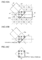
- a wide oblique line 43 overlaps the end portion of a wide horizontal line 41, and an assembled connection pattern 45A is placed in the overlapped area.
- a wide horizontal line 41 is produced.
- a wide oblique line 43 extending at an oblique angle (135 degrees in Fig. 10) with respect to the horizontal line 41 is produced.
- an assembled connection pattern 45A is placed at the intersection of the oblique line 43 and the horizontal line 41.
- Fig. 10B shows the top metal 43a of the connection pattern 45A, which makes use of the end portion of the oblique line 43, and the cuts 47 arranged at a predetermined interval inside the overlapped area.
- Fig. 10C shows the bottom metal 41a, which makes use of the end portion of the horizontal line 41, and the cuts 47.
- one of the cuts 47 must be positioned at the intersection of the center line 42 of the horizontal line 41 and the center line 44 of the oblique line 43.
- the other cuts 47 are positioned at the grid points of the orthogonal coordinate system inside the overlapped area.
- the top metal 43a is a rectangle rotated by 45 degrees with respect to the square bottom metal 41a.
- the rectangular top metal is generated using orthogonal lines only, and therefore, the amount of data does not increase. In addition, there is almost no projection that comes out of the contour of lines, and deletion process is unnecessary.
- connection pattern 35A shown in Fig 10 has overhangs in which cuts cannot be applied.
- both the top metal 43a and the bottom metal 41a have triangle areas (i.e., overhangs) in which no cuts are defined.
- the maximum number of cuts under the adapted design rule are defined in the overlapped area, and as a result, the total number of cuts in the assembled connection pattern becomes greater than the number of the independent connection patterns used in the third embodiment. This further results in that the resistance of the via-contact manufactured from the assembled connection pattern is reduced, as compared with the arrangement shown in Fig. 9.
- Fig. 11 illustrates another layout of terminal connection using an assembled connection pattern.
- a wide horizontal line 41 is produced, and a wide oblique line 43 is produced so that its end portion sufficiently overlaps the end portion of the horizontal line 41.
- a square assembled connection pattern 45B is placed in the overlapped area.
- the overlapped area between the horizontal line 41 and the oblique line 43 is larger than the overlapped area of the assembled connection pattern 45A shown in Fig. 10.
- the projection 46 (Fig. 11A) coming out of the contour of the line becomes large.
- the assembled connection pattern 45B consists of a square top metal 43b, which makes use of the end portion of the oblique line 43, a square bottom metal 41b, which makes use of the end portion of the horizontal line 41, and multiple cuts 47.
- the cuts are positioned at the grid points inside the overlapped area.
- One of the cut is positioned at the intersection of the center line 42 of the horizontal line 41 and the center line 44 of the oblique line 43 within the square of the bottom metal 41b.
- the layout of Fig. 11 is superior in that the assembled connection pattern is created in the easiest manner on CAD because it consists of squares only. This layout allows the minimum amount of data processing because of the easy connection pattern and no deletion of the projection.
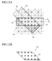
- Fig. 12 illustrates a terminal layout of two lines using an assembled connection pattern of parallelogram.
- a wide horizontal line 51 is produced, and a wide oblique line 53 is produced so that the end portion sufficiently overlaps the end portion of the horizontal line 51.
- An assembled connection pattern 55 of a parallelogram is placed in the overlapped area.
- the wiring layout program becomes slightly complicated because deletion of projections is required. However, the line shape is greatly simplified, and adverse influence to the coupling capacitance can be prevented. It is better to prepare the parallelogramic connection pattern 55 in advance on the program. This layout can guarantee reliable connection between the horizontal line and the oblique line located in different layers because of sufficient overlapped area and the increased number of cuts.
- the first through fifth embodiments illustrate the terminal layouts for connecting two lines located in different layers.
- a terminal layout for connection of an oblique line and a basic orthogonal line located in the same layer is provided.
- a horizontal line 61 with the minimum line width W is produced, and an oblique line 63 with the minimum width ⁇ 2 W is produced.
- the CAD recognizes the intersection 68 of the center line 62 of the horizontal line 61 and the center line 64 of the oblique line 63, and therefore, it recognizes that these two lines cross each other.
- the CAD also needs to know that these two lines 61 and 61 must be actually connected to each other, in addition to the fact that the two lines cross each other at the intersection 68.
- a plane connection pattern 65A must be placed in the overlapped area between the horizontal line 61 and the oblique line 63.
- a connection pattern for connecting those lines located in the same layer is called a "turn via".
- the plane connection pattern (i.e., the turn via) 65A consists of two squares. As show in Fig. 13B, the line width of the horizontal line 61 is W, and the line width of the oblique line 63 is ⁇ 2 W. Thus, the square 61a, which is the end portion of the horizontal line 61, is completely included in the square 63a, which is the end portion of the oblique line 63. Since the turn via 65A is easy to produce because of the simple combination of two squares, the terminal layout using an automatic layout design technique is greatly simplified when connecting an oblique line and a basic orthogonal line in the same layer at their end portions.
- Fig. 14 illustrates another terminal layout for connecting two lines having the same line width and located in the same layer.
- a horizontal line 67 with a width of ⁇ 2 W is produced, and an oblique line 63 with the same width ⁇ 2 W is produced.
- a turn via 65B is placed at the intersection 68 of the center line 69 of the horizontal line 67 and the center line 64 of the oblique line 63.
- the turn via (or the plane connection pattern) 65B is a combination of two squares of the same size, one of which is rotated by 45 degrees with respect to the other.
- the seventh embodiment illustrates how a semiconductor device having a three-dimensional oblique line structure is manufactured from a layout produced by the automatic layout design technique described above. To manufacture such a semiconductor device, a mask set is prepared from the layout.
- Fig. 15 is a schematic plan view of a cell 70, which is a part of a semiconductor integrated circuit, formed on a semiconductor substrate.
- An oblique line structure in which oblique lines 73 and basic orthogonal lines (including horizontal lines 71) exist in a transistor region 72 of the cell 70, is schematically illustrated. The detailed line structure is omitted from this figure for the convenience of explanation.
- the mask pattern layout data produced by the aforementioned automatic design technique is inputted to a pattern generator, such as an optical exposure device, an electron beam exposure device, and an X-ray exposure device.
- the layout data is used to print the line patterns onto reticles (that is, exposure masks).
- the number of reticles used to manufacture a semiconductor integrated circuit is from ten to several tens, or more, depending on the steps of the manufacturing process or the scale of the semiconductor.
- Fig. 16 illustrates three reticles, which is only a part of an actual reticle set.
- the three masks are referred to as a mask set 75, each mask shows only a part of patterns for the convenience sake.
- the mask set 75 includes a first mask 75A, a second mask 75B, and a third mask 75C.
- the first mask 75A has opaque line patterns (light-blocking region) 76A formed of, for example, a chromium (Cr) film on a, for example, a quartz mask substrate.
- the opaque line patterns correspond to horizontal lines of a first wiring layer.
- the second mask 75B has apertures (i.e., transparent regions) 76B, which become cut patterns of via holes.
- the third mask 75C has oblique line patterns (i.e., opaque regions) 76C that extend at an oblique angle (e.g., 45 degrees or 135 degrees) with respect to the first line patterns 76A. If the first, second, and third masks are superimposed, the terminal ends of the oblique line patterns 76C and the terminal ends of the horizontal line patterns 75A are aligned with the cut patterns 76B.
- Fig. 15 The three-dimensional oblique line structure illustrated in Fig. 15 is achieved using a series of reticles that includes the mask set 75 shown in Fig. 16. It is needless to say that various other masks are required to for transistors or other interconnections of a semiconductor integrated. However, explanation for other masks will be omitted.
- Fig. 17 is a schematic sectional view of a part of a semiconductor integrated circuit with an oblique line structure 80.
- the oblique line structure 80 comprises basic orthogonal lines 81 extending in the horizontal or the vertical direction on the first insulating layer on the silicon (Si) substrate 90, and oblique lines 83 located above the basic orthogonal lines via the second insulating layer 94.
- the oblique lines 83 extend at an angle of 45 degrees or 135 degrees with respect to the orthogonal lines 81.
- Via-contacts 85 connect the orthogonal lines and the oblique lines at their end portions or the intersections.
- each via-contact is a square whose two facing sides are along the longitudinal edges of the narrower line, either the oblique line or the orthogonal line (the latter one in the example shown in Fig. 17).
- the oblique lines 83 are covered with a passivation layer or the third insulating layer 99.
- the via-contact 85 is made of a conductive material, such as tungsten (W), filled in a via-hole formed based on the layout designed by the automatic design method of the present invention.
- An upper oblique line 83 and a lower orthogonal line 81 are connected by one or more via-contacts 85 inside the overlapped area of these two lines.
- One of the via-contacts 85 is located at the intersection of the center line of the oblique line 83 and the center line of the orthogonal line 81.
- first through third insulating layers are shown in Fig. 17 for the convenience sake, there may be other insulating layers and lower wiring layers.
- Fig. 18 illustrates the steps of fabricating the oblique line structure 80 shown in Fig. 17 using the mask set 75 illustrated in Fig. 16.
- first metal film 81 and second metal film 97 are connected by via-contacts.
- there may be three-dimensional connection structures for example, connection between a third metal film and a fourth metal film located in different wiring layers.
- the line patterns may be printed directly onto the wafer without using the mask set.
- the line patterns are written by scanning, for example, an electron beam based on the layout data of the automatic layout design.
- At least one of the first metal film 81 and second metal film 97 may not be made of Al allow.
- either or both metal films may be made of copper (Cu), and Damascene wiring structures may be employed.
- Fig. 19 illustrates a semiconductor integrated circuit 100 having a clock tree composed of oblique lines.
- the semiconductor integrated circuit 100 comprises a PLL (phase locked loop) 110 positioned at a corner of the chip, and a main clock line 101 extending obliquely from the PLL at an angle of 45 degrees with respect to the orthogonal coordinate axes of the chip.
- the main clock line 101 terminates at or near the center of the chip.
- a clock tree branches off symmetrically from the terminal end C of the main clock line into oblique directions at an angle of 45 degrees or 135 degrees with respect to the orthogonal coordinate axes.
- the bold numbers 1 through 5 represent the branching hierarchy of the clock tree.
- the oblique line 102 of the second branching hierarchy extends symmetrically from the terminal end C of the main clock line 101 in a direction perpendicular to the main clock line 101.
- oblique lines 103a and 103b of the third branching hierarchy extend again symmetrically with respect to the terminal end C of the main clock line 101.
- oblique lines 104a through 104d of the fourth branching hierarchy extend symmetrically with respect to the main clock line 101. In this manner, as the branching hierarchy lowers, each line branches off symmetrically with respect to the main clock line.
- a clock tree consisting of oblique lines is spread symmetrically with respect to the center C of the chip.
- a basic orthogonal line patterns are formed below the clock tree.
- the end portions of the oblique lines of the tree are connected to the end portions or the intersections of the orthogonal lines of the lower layer through via-contacts according to the terminal layout generated by the automatic design method of the invention.
- the lines in the same branching hierarchy always belong to the same layer. Therefore, the four oblique lines 104a through 104b in the fourth branching hierarchy belong to the same layer.
- Those lines that belong to different hierarchies, but extend in the same direction may be located in the same layer, or alternatively, they may be located in different layer.
- the oblique lines 103 in the third branching hierarchy and the oblique lines 105 in the fifth hierarchy in Fig. 19 may be located in the same layer because they all extend in the same direction.
- the most significant effect of using the oblique lines resides in that balances in circuit design, such as load capacitance, are easily computed. In addition, variations in clock delay due to process fluctuation can be reduced. Since the lines in the same branching hierarchy are arranged in the same layer so as to be symmetrical, variations among different wiring layers are eliminated. Pulses are supplied through symmetrical shorter paths, clock delay between two arbitrary points is reduced, while balancing the load capacitance for each branch.
- the line width is narrowed based on the Elmore's wiring delay computation formula.
- the current density flowing through the interconnection becomes small as branching proceeds. Accordingly, the line width can be narrowed within the range not exceeding the acceptable value of the current density of the metal line.
- the clock tree structure of oblique lines can realize a high-performance integrated circuit with less load capacitance and variation.
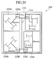
- Fig. 20 illustrates a layout of a part of an LSI, to which the clock tree illustrated in the eighth embodiment is applied.
- the integrated circuit 200 comprises a main PLL 210 positioned at an end of the circuit, a global clock line 212 extending from the main PLL 210, and a plurality of random blocks 230A to 230C.
- the main PLL 210 supplies a global clock of a comparatively low frequency (some hundreds MHz).
- Each random block 230 includes a clock driver cell connected to the global clock line 212, and a clock tree composed of oblique lines.
- the clock driver cell is a DLL (delay-locked loop) 220 in the eighth embodiment.
- the main PPL 210 adjusts the phases of clocks between the integrated circuit 200 and other integrated circuits (not shown).
- a global clock which is a basic clock for the overall chip, is supplied to a circuit block or a random block inside the chip.
- a random block is a set of partial circuits including multiple logical circuit modules designed by, for example, an engineer, in a dividing manner.
- the DLL 220 provided in each random block converts a global clock of a comparatively low frequency into a local clock of a high frequency (several GHz), and supplies the high-frequency clock inside of the random block via the associated clock tree.
- the clock tree of each block 230 is connected to the basic orthogonal lines in a lower layer by via-contacts.
- the terminal ends of the oblique lines configuring the clock tree are securely connected to the terminal end of the basic orthogonal lines by the via-contacts based on the layout produced by the automatic design method.
- the wiring delay is greatly affected by the wiring resistance and capacitance.
- a pulse rate of several hundreds MHz is the upper limit for synchronizing a chip of 10 mm square. If a higher rate is desired, the thickness of the clock lines must be increased to some tens to some hundreds times of a standard signal line. The manufacture process of such thick lines is difficult, and it is difficult to handle such thick lines on CAD.
- a global clock is fed at a comparatively low frequency, and is converted into a high frequency for each random block.
- the local blocks are synchronized with one another by the high frequency signal.
- This arrangement allows faster operation in a chip of a conventional size.
- a clock tree consisting of symmetrical oblique lines, a delay is reduced.
- random blocks 230 are disposed on both sides of the global clock line 212. Accordingly, the DLL of each random block 230 can be positioned along the periphery of the circuit, which allows a voltage to be supplied easily.
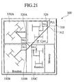
- Fig. 21 illustrates a modification of the semiconductor integrated circuit of Fig. 20.
- a PLL 310 is positioned at a corner of the circuit, and a global clock line 312 for supplying a global clock is arranged obliquely.
- a delay is likely to be caused among global clock lines for supplying a global clock.
- the configuration shown in Fig. 21 is advantageous in that the delay cased in the global clock line is reduced because of its oblique arrangement.
- the DLLs 320 of the random blocks are gathered around the end of the global clock line 312 in order to supply the global clock to the respective random blocks 330 at a high speed almost simultaneously.
- a power is supplied to each DDL from a dedicated pad (not shown) attached to the top face of the chip.
- the frequency of the global clock itself can be increased. This achieves a faster circuit operation.
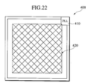
- FIG. 22 shows an example of a semiconductor integrated circuit that has a clock mesh of oblique lines.
- a semiconductor integrated circuit 400 comprises a PLL 410 positioned at a corner of a chip, and a clock mesh 420 consisting of oblique lines. The clock mesh is arranged almost over the chip.
- clock supply lines in a mesh structure have less process variations. Accordingly, variations due to a delay can also be reduced over the entire region of the circuit. Because the clock mesh of oblique lines is used in the tenth embodiment, the clock delay is further reduced, as compared with a conventional clock mesh consisting of horizontal and vertical lines.
- a basic orthogonal wiring layer that is connected directly to the cell may be located below the clock mesh of the oblique lines.
- the end portions of the orthogonal lines are connected to the oblique lines of the clock mesh by via-contact according to the layout produced by the automatic layout design of the invention.
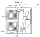
- FIG. 23 illustrates a part of an LSI, to which clock mesh shown in Fig. 22 is applied.
- a semiconductor integrated circuit 500 comprises a main PLL 510 positioned along the periphery of the circuit, a global clock line 512 extending from the main PLL 510, and a plurality of random blocks 530.
- the global clock line 512 supplies a global clock at a comparatively low frequency (e.g., some hundreds MHz).
- Each random block 530 has a clock driver cell (DLL in the eleventh embodiment) 520 connected to the global clock line 512, and an oblique clock mesh 540 of oblique lines.
- the DLL 520 converts a global clock of a comparatively low frequency into a high-frequency (several GHz) local clock, and supplies the high-frequency local clock inside the random block via the associated clock mesh 540.
- a basic orthogonal wiring layer may be furnished below the clock mesh 540 in each random block 530.
- the end portions of the orthogonal lines of the lower layer are connected to the cell by via-contact fabricated from the terminal layout produced by the automatic design method of the invention.
- the DLL 520 synchronizes a supplied global clock with the clocks in the other blocks at a high frequency.
- a high-frequency signal is supplied from the DLL 520 to each site via the oblique clock mesh that has little delay variation. This arrangement allows a fast operation of the circuit.
- the vertical global clock supply line 512 may be run obliquely across the chip, as in the example shown in FIG. 21. In this case, the frequency of the global clock itself can be increased, which results in faster operation of the circuit.
- FIG. 24 illustrates still another example of a semiconductor integrated circuit using a clock mesh.
- a semiconductor integrated circuit 600 comprises a route driver 610 positioned at a corner of the chip, a main clock supply line 612 extending obliquely from the route driver 610 across the chip, and a clock mesh 630 covering the entire area of the chip.
- Multiple sub-drivers 620 are connected to the main clock supply line 612.
- the main clock supply line 612 has a comparatively large driving force.
- the sub-drivers 620 drive the oblique lines that form the clock mesh 630.
- a skew of the clock signal which is the most problematic in a logical LSI, can be reduced. Variation in the manufacturing process is also reduced.
- FIG. 25 shows still another example of a semiconductor integrated circuit employing a clock mesh structure.
- a semiconductor integrated circuit 700 comprises a route driver 710 positioned near the edge of the circuit, a main clock supply line 712 extending from the route driver 710 along the periphery of the circuit, and a clock mesh 730 spread over the circuit.
- Multiple sub-drivers 720 are connected to the main clock supply line 712.
- the root driver 710 has a comparatively large driving force.
- the sub-drivers drive the associated oblique lines of the clock mesh 630.
- the feature of the semiconductor integrated circuit 700 is that the sub-drivers 720 are arranged along the periphery of the circuit.
- the sub-drivers 620 that can be a source of noise are disposed deep inside the circuit.
- the noise sources are placed along the periphery of the circuit in the thirteenth embodiment. This arrangement is unlikely to cause a voltage drop. Since a voltage drop causes a difference in performance between the center and the periphery of the circuit. To this end, the configuration shown in Fig. 25 is superior in achieving a uniform performance.
- FIG. 26 is a schematic block diagram of an automatic design apparatus that carries out the automatic design method according to the invention.
- An automatic design apparatus 1000 comprises a program database 1003 for storing an automatic design program, a layout database 1005 for storing layout data, a process controller 1007 for controlling the data processing of the automatic layout design.
- the apparatus also has a layout display 1009 for displaying a layout produced by the automatic design apparatus, an input device 1011 for inputting patterns or and figures, and an output device 1013 for output the layout produced by automatic design apparatus.
- the process controller 1007 includes a rule checker 1021 for checking the design rules and the electrical rules, an automatic routing 1023 for automatically selecting a signal-transfer path and a bypass route of layout data; and a graphic editor 1025 for editing the produced layout.
- the layout database 1005 stores circuit diagrams that have already been produced, and a variety of lines and connection patterns of various widths and shapes.
- the program database 1003 stores a program for automatically designing a layout.
- the program allows the automatic design apparatus to produce a wiring layout on a two-dimensional plane, and defining connection patterns at desired positions for connecting wiring patterns of different layers or the same layer.
- This program may be temporarily stored in a magnetic disk, an optical disk, a magneto-optical disk, or a magnetic tape (specifically, floppy disks, CD-ROMs, MO disks, or cassette tapes) before it is stored in the program database 1005.
- the automatic design program includes at least the following steps:
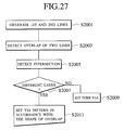
- Fig. 27 is a flow chart of terminal processing of two lines to be connected, that is carried out by the automatic design apparatus based on the program stored in the program database 1003.
- step S2001 first and second lines are produced based on the information inputted from the input unit 1011 shown in Fig. 26.
- the first line extends, for example, along the basic orthogonal coordinate axes.
- the second line extends at an oblique angle with respect to the first line.
- the process controller 1007 detects an overlapped area of the end portions of the first and second.
- step S2005 the intersection of the center line of the first line and the center line of the second line is detected inside the overlapped area.
- step S2007 it is determined whether or not the first and second lines are located in different layers based on the information inputted from the input unit 1011. If NO in step S2007 (that is, if the first and second lines are in the same layer), the process proceeds to step S2009, in which a turn VIA is placed at the intersection in the overlapped area. This indicates that the first and second lines are connected to each other in the same layer. If YES in step S2007, the process jumps to step S2011, and a connection pattern is selected in accordance with the shape of the overlapped area, and placed at the intersection in the overlapped area.
- the detected overlapped area is a rectangular region located at the terminal end of two lines with the minimum width
- a standard via is read from the layout database 1005, and set at the intersection.
- the detected overlapped area is a parallelogram or a quadrangle having an oblique side located at the terminal end of two lines with the minimum width
- a connection pattern of parallelogram is read out of the layout database 1005, and placed at the intersection.
- Such parallologramic connection pattern is generated in advance, and stored in the data. If the first and second lines are wide lines, an assembled connection pattern may be read according to the shape of the overlapped area.
- a square standard via and an assembled via having a set of standard cuts are patterns formed of a combination of orthogonal lines only. When using these patterns, the amount of data is small, and therefore, the readout time and writing time are reduced.
- step S2003 it may be determined whether or not there is a request for deletion of an unnecessary projection coming out of the overlapped area after step S2003. If a request for deletion occurs, the unnecessary projection is deleted.
- the layout data including oblique lines processed by the automatic design program is monitored on the layout display 1009.
- the layout data is inputted to a pattern generator, which creates a mask pattern for each layer based on the layout data.
- a mask set consisting of a predetermined number of the masks (or reticles)
- a semiconductor integrated circuit is fabricated by photolithography using an exposure apparatus, such as a stepper.
- arrangement of random blocks and the positions of the DLLs in the semiconductor integrated circuit may be changed arbitrarily as long as the frequency of the global clock can be converted into a high frequency.
- the amount of computation on CAD is also reduced, and the design rule is easily verified.
- Most part of the mask patters of the mask set of the present invention is generated from the orthogonal data, which improves alignment of patterns in different layers.
- the semiconductor integrated circuit having an oblique line structure can reduce a wiring delay efficiently.
- the semiconductor integrated circuit of the present invention supplies a clock via a clock-supply structure of oblique lines.
- the clock signal supplied through the oblique line structure is hardly affected by the variation in process or capacitance among different layers. Consequently, a skew of the clock signal is reduced.
- the frequency of a global clock itself which is generally driven at a comparatively low frequency, can be increased.
- the low-frequency global clock is converted into a high frequency local clock, and the local clock is supplied throughout the block via a clock supply network formed by oblique lines. Under this arrangement, a delay of the entire circuit can be significantly reduced.
- a recording medium containing the automatic design program of the present invention enables a CAD to process a terminal layout of connection between an oblique line and an orthogonal line at a high efficiency.
Landscapes
- Engineering & Computer Science (AREA)
- Theoretical Computer Science (AREA)
- Physics & Mathematics (AREA)
- General Engineering & Computer Science (AREA)
- General Physics & Mathematics (AREA)
- Computer Hardware Design (AREA)
- Computer Networks & Wireless Communication (AREA)
- Evolutionary Computation (AREA)
- Geometry (AREA)
- Design And Manufacture Of Integrated Circuits (AREA)
- Preparing Plates And Mask In Photomechanical Process (AREA)
- Semiconductor Integrated Circuits (AREA)
Applications Claiming Priority (2)
| Application Number | Priority Date | Filing Date | Title |
|---|---|---|---|
| JP32737099A JP3822009B2 (ja) | 1999-11-17 | 1999-11-17 | 自動設計方法、露光用マスクセット、半導体集積回路装置、半導体集積回路装置の製造方法、および自動設計プログラムを記録した記録媒体 |
| JP32737099 | 1999-11-17 |
Publications (2)
| Publication Number | Publication Date |
|---|---|
| EP1102182A2 true EP1102182A2 (de) | 2001-05-23 |
| EP1102182A3 EP1102182A3 (de) | 2009-03-18 |
Family
ID=18198393
Family Applications (1)
| Application Number | Title | Priority Date | Filing Date |
|---|---|---|---|
| EP00124343A Withdrawn EP1102182A3 (de) | 1999-11-17 | 2000-11-17 | Verfahren zum automatischen Entwurf eines Layouts für LSI, Maskensatz und nach dem Verfahren hergestellte integrierte Halbleiterschaltung, und Aufzeichnungsmedium zur Speicherung des Programms |
Country Status (6)
| Country | Link |
|---|---|
| US (2) | US6546540B1 (de) |
| EP (1) | EP1102182A3 (de) |
| JP (1) | JP3822009B2 (de) |
| KR (2) | KR100402222B1 (de) |
| CN (1) | CN1169204C (de) |
| TW (1) | TW486645B (de) |
Cited By (3)
| Publication number | Priority date | Publication date | Assignee | Title |
|---|---|---|---|---|
| GB2368463A (en) * | 2000-07-11 | 2002-05-01 | Hewlett Packard Co | Optimising the size and placement of contact elements in integrated circuits |
| WO2003019620A3 (en) * | 2001-08-21 | 2003-08-28 | Sun Microsystems Inc | Technique to minimize crosstalk in electronic packages |
| WO2004006328A1 (ja) * | 2002-07-09 | 2004-01-15 | Sony Corporation | 半導体装置およびその製造方法 |
Families Citing this family (107)
| Publication number | Priority date | Publication date | Assignee | Title |
|---|---|---|---|---|
| JP2000211993A (ja) * | 1999-01-22 | 2000-08-02 | Mitsubishi Electric Corp | 半導体ウェハの製造方法、半導体製造装置、および、半導体装置 |
| JP3390393B2 (ja) * | 1999-12-21 | 2003-03-24 | エヌイーシーマイクロシステム株式会社 | 自動配置配線システムの配線方法および自動配置配線システムの配線方法を記録した記録媒体 |
| US6889372B1 (en) | 2000-07-15 | 2005-05-03 | Cadence Design Systems Inc. | Method and apparatus for routing |
| US6898773B1 (en) | 2002-01-22 | 2005-05-24 | Cadence Design Systems, Inc. | Method and apparatus for producing multi-layer topological routes |
| US7024650B2 (en) * | 2000-12-06 | 2006-04-04 | Cadence Design Systems, Inc. | Method and apparatus for considering diagonal wiring in placement |
| US6516455B1 (en) * | 2000-12-06 | 2003-02-04 | Cadence Design Systems, Inc. | Partitioning placement method using diagonal cutlines |
| US7003754B2 (en) * | 2000-12-07 | 2006-02-21 | Cadence Design Systems, Inc. | Routing method and apparatus that use of diagonal routes |
| US6826737B2 (en) * | 2000-12-06 | 2004-11-30 | Cadence Design Systems, Inc. | Recursive partitioning placement method and apparatus |
| US7055120B2 (en) * | 2000-12-06 | 2006-05-30 | Cadence Design Systems, Inc. | Method and apparatus for placing circuit modules |
| US6957410B2 (en) * | 2000-12-07 | 2005-10-18 | Cadence Design Systems, Inc. | Method and apparatus for adaptively selecting the wiring model for a design region |
| AU2002233977A1 (en) * | 2000-12-06 | 2002-06-18 | Simplex Solutions, Inc. | Method and apparatus for considering diagonal wiring in placement |
| US7080336B2 (en) * | 2000-12-06 | 2006-07-18 | Cadence Design Systems, Inc. | Method and apparatus for computing placement costs |
| US7073150B2 (en) * | 2000-12-07 | 2006-07-04 | Cadence Design Systems, Inc. | Hierarchical routing method and apparatus that use diagonal routes |
| US6915501B2 (en) | 2001-01-19 | 2005-07-05 | Cadence Design Systems, Inc. | LP method and apparatus for identifying routes |
| US6738960B2 (en) * | 2001-01-19 | 2004-05-18 | Cadence Design Systems, Inc. | Method and apparatus for producing sub-optimal routes for a net by generating fake configurations |
| JP2002312414A (ja) * | 2001-04-13 | 2002-10-25 | Toshiba Corp | 半導体集積回路装置のレイアウト設計システム、配線設計方法、配線設計プログラム及び半導体集積回路装置の製造方法 |
| JP2002329783A (ja) | 2001-04-27 | 2002-11-15 | Toshiba Corp | 配線パターンの自動レイアウト方法、レイアウトパターンの光学補正方法、自動レイアウト方法と光学補正方法に基づいて製造される半導体集積回路、および自動レイアウト光学補正プログラムを記録した記録媒体 |
| US6957408B1 (en) | 2002-01-22 | 2005-10-18 | Cadence Design Systems, Inc. | Method and apparatus for routing nets in an integrated circuit layout |
| US6877146B1 (en) | 2001-06-03 | 2005-04-05 | Cadence Design Systems, Inc. | Method and apparatus for routing a set of nets |
| US7107564B1 (en) | 2001-06-03 | 2006-09-12 | Cadence Design Systems, Inc. | Method and apparatus for routing a set of nets |
| US6895569B1 (en) | 2001-06-03 | 2005-05-17 | Candence Design Systems, Inc. | IC layout with non-quadrilateral Steiner points |
| US6882055B1 (en) | 2001-06-03 | 2005-04-19 | Cadence Design Systems, Inc. | Non-rectilinear polygonal vias |
| US6859916B1 (en) * | 2001-06-03 | 2005-02-22 | Cadence Design Systems, Inc. | Polygonal vias |
| US7310793B1 (en) | 2001-06-03 | 2007-12-18 | Cadence Design Systems, Inc. | Interconnect lines with non-rectilinear terminations |
| US6957411B1 (en) | 2001-06-03 | 2005-10-18 | Cadence Design Systems, Inc. | Gridless IC layout and method and apparatus for generating such a layout |
| US6976238B1 (en) | 2001-06-03 | 2005-12-13 | Cadence Design Systems, Inc. | Circular vias and interconnect-line ends |
| US6829757B1 (en) | 2001-06-03 | 2004-12-07 | Cadence Design Systems, Inc. | Method and apparatus for generating multi-layer routes |
| US6951005B1 (en) | 2001-06-03 | 2005-09-27 | Cadence Design Systems, Inc. | Method and apparatus for selecting a route for a net based on the impact on other nets |
| US7069530B1 (en) | 2001-06-03 | 2006-06-27 | Cadence Design Systems, Inc. | Method and apparatus for routing groups of paths |
| JP4929437B2 (ja) * | 2001-08-03 | 2012-05-09 | 富士通セミコンダクター株式会社 | 集積回路の配線レイアウト方法 |
| US6795958B2 (en) | 2001-08-23 | 2004-09-21 | Cadence Design Systems, Inc. | Method and apparatus for generating routes for groups of related node configurations |
| US7398498B2 (en) | 2001-08-23 | 2008-07-08 | Cadence Design Systems, Inc. | Method and apparatus for storing routes for groups of related net configurations |
| US7143382B2 (en) | 2001-08-23 | 2006-11-28 | Cadence Design Systems, Inc. | Method and apparatus for storing routes |
| US7155697B2 (en) * | 2001-08-23 | 2006-12-26 | Cadence Design Systems, Inc. | Routing method and apparatus |
| US6931616B2 (en) * | 2001-08-23 | 2005-08-16 | Cadence Design Systems, Inc. | Routing method and apparatus |
| US7058913B1 (en) * | 2001-09-06 | 2006-06-06 | Cadence Design Systems, Inc. | Analytical placement method and apparatus |
| US7080329B1 (en) | 2002-01-22 | 2006-07-18 | Cadence Design Systems, Inc. | Method and apparatus for identifying optimized via locations |
| US6938234B1 (en) | 2002-01-22 | 2005-08-30 | Cadence Design Systems, Inc. | Method and apparatus for defining vias |
| US6892371B1 (en) | 2002-01-22 | 2005-05-10 | Cadence Design Systems, Inc. | Method and apparatus for performing geometric routing |
| US7117468B1 (en) | 2002-01-22 | 2006-10-03 | Cadence Design Systems, Inc. | Layouts with routes with different spacings in different directions on the same layer, and method and apparatus for generating such layouts |
| US6944841B1 (en) | 2002-01-22 | 2005-09-13 | Cadence Design Systems, Inc. | Method and apparatus for proportionate costing of vias |
| US7089524B1 (en) | 2002-01-22 | 2006-08-08 | Cadence Design Systems, Inc. | Topological vias route wherein the topological via does not have a coordinate within the region |
| US7013451B1 (en) | 2002-01-22 | 2006-03-14 | Cadence Design Systems, Inc. | Method and apparatus for performing routability checking |
| US7096449B1 (en) | 2002-01-22 | 2006-08-22 | Cadence Design Systems, Inc. | Layouts with routes with different widths in different directions on the same layer, and method and apparatus for generating such layouts |
| US7036105B1 (en) | 2002-01-22 | 2006-04-25 | Cadence Design Systems, Inc. | Integrated circuits with at least one layer that has more than one preferred interconnect direction, and method for manufacturing such IC's |
| JP3767520B2 (ja) | 2002-06-12 | 2006-04-19 | 日本電気株式会社 | 集積回路装置 |
| US6769103B2 (en) | 2002-07-19 | 2004-07-27 | Micron Technology, Inc. | Line width check in layout database |
| JP4373065B2 (ja) * | 2002-09-20 | 2009-11-25 | 株式会社日立製作所 | 半導体装置およびその製造方法 |
| US7093221B2 (en) | 2002-11-18 | 2006-08-15 | Cadence Design Systems, Inc. | Method and apparatus for identifying a group of routes for a set of nets |
| US7047513B2 (en) | 2002-11-18 | 2006-05-16 | Cadence Design Systems, Inc. | Method and apparatus for searching for a three-dimensional global path |
| US7010771B2 (en) | 2002-11-18 | 2006-03-07 | Cadence Design Systems, Inc. | Method and apparatus for searching for a global path |
| US6988257B2 (en) | 2002-11-18 | 2006-01-17 | Cadence Design Systems, Inc. | Method and apparatus for routing |
| US7624367B2 (en) | 2002-11-18 | 2009-11-24 | Cadence Design Systems, Inc. | Method and system for routing |
| US7080342B2 (en) | 2002-11-18 | 2006-07-18 | Cadence Design Systems, Inc | Method and apparatus for computing capacity of a region for non-Manhattan routing |
| US7003752B2 (en) | 2002-11-18 | 2006-02-21 | Cadence Design Systems, Inc. | Method and apparatus for routing |
| US6892369B2 (en) | 2002-11-18 | 2005-05-10 | Cadence Design Systems, Inc. | Method and apparatus for costing routes of nets |
| US7171635B2 (en) | 2002-11-18 | 2007-01-30 | Cadence Design Systems, Inc. | Method and apparatus for routing |
| US7480885B2 (en) | 2002-11-18 | 2009-01-20 | Cadence Design Systems, Inc. | Method and apparatus for routing with independent goals on different layers |
| US7216308B2 (en) | 2002-11-18 | 2007-05-08 | Cadence Design Systems, Inc. | Method and apparatus for solving an optimization problem in an integrated circuit layout |
| US6996789B2 (en) | 2002-11-18 | 2006-02-07 | Cadence Design Systems, Inc. | Method and apparatus for performing an exponential path search |
| US6936898B2 (en) * | 2002-12-31 | 2005-08-30 | Transmeta Corporation | Diagonal deep well region for routing body-bias voltage for MOSFETS in surface well regions |
| US7089519B1 (en) | 2002-12-31 | 2006-08-08 | Cadence Design System, Inc. | Method and system for performing placement on non Manhattan semiconductor integrated circuits |
| US7013445B1 (en) | 2002-12-31 | 2006-03-14 | Cadence Design Systems, Inc. | Post processor for optimizing manhattan integrated circuits placements into non manhattan placements |
| US7506295B1 (en) | 2002-12-31 | 2009-03-17 | Cadence Design Systems, Inc. | Non manhattan floor plan architecture for integrated circuits |
| US6934929B2 (en) * | 2003-01-13 | 2005-08-23 | Lsi Logic Corporation | Method for improving OPC modeling |
| JP2004228164A (ja) | 2003-01-20 | 2004-08-12 | Toshiba Corp | 半導体集積回路及びその製造方法 |
| JP2004289007A (ja) * | 2003-03-24 | 2004-10-14 | Toshiba Corp | クロック配線、クロックレイアウトシステム及びクロックレイアウト方法 |
| US7243328B2 (en) * | 2003-05-07 | 2007-07-10 | Cadence Design Systems, Inc. | Method and apparatus for representing items in a design layout |
| US7065731B2 (en) * | 2003-05-07 | 2006-06-20 | Cadence Design Systems, Inc. | Removal of acute angles in a design layout |
| US7080339B2 (en) * | 2003-05-07 | 2006-07-18 | Cadence Design Systems, Inc. | Plane representation of wiring in a design layout |
| JP4245418B2 (ja) | 2003-06-25 | 2009-03-25 | 富士通マイクロエレクトロニクス株式会社 | 斜め方向配線を有する半導体集積回路装置及びそのレイアウト方法 |
| TWI246138B (en) * | 2003-09-08 | 2005-12-21 | Realtek Semiconductor Corp | Method for checking via density in IC layout |
| JP4509521B2 (ja) * | 2003-10-01 | 2010-07-21 | 東芝マイクロエレクトロニクス株式会社 | 自動設計方法、自動設計装置、レチクルセット、半導体集積回路及び設計プログラム |
| US7174528B1 (en) | 2003-10-10 | 2007-02-06 | Transmeta Corporation | Method and apparatus for optimizing body bias connections in CMOS circuits using a deep n-well grid structure |
| US7049699B1 (en) * | 2003-11-12 | 2006-05-23 | Transmeta Corporation | Low RC structures for routing body-bias voltage |
| US7328417B2 (en) * | 2003-12-09 | 2008-02-05 | Lsi Logic Corporation | Cell-based method for creating slotted metal in semiconductor designs |
| JP4357287B2 (ja) * | 2003-12-18 | 2009-11-04 | 株式会社東芝 | 修正指針の発生方法、パターン作成方法、マスクの製造方法、半導体装置の製造方法及びプログラム |
| JP2005208473A (ja) * | 2004-01-26 | 2005-08-04 | Toshiba Corp | 自動設計装置,自動設計方法,及びこれらを用いて製造可能なレチクルセット,半導体集積回路 |
| US7645673B1 (en) * | 2004-02-03 | 2010-01-12 | Michael Pelham | Method for generating a deep N-well pattern for an integrated circuit design |
| JP2005268748A (ja) * | 2004-02-18 | 2005-09-29 | Nec Electronics Corp | 半導体装置及びその製造方法 |
| US7388260B1 (en) * | 2004-03-31 | 2008-06-17 | Transmeta Corporation | Structure for spanning gap in body-bias voltage routing structure |
| US7448012B1 (en) | 2004-04-21 | 2008-11-04 | Qi-De Qian | Methods and system for improving integrated circuit layout |
| JP4464218B2 (ja) * | 2004-07-16 | 2010-05-19 | Necエレクトロニクス株式会社 | Lsi設計システム、lsi設計方法、及びレイアウトデータ構造 |
| JP4801333B2 (ja) * | 2004-07-23 | 2011-10-26 | パナソニック株式会社 | 電源配線構造および該電源配線構造を備えた半導体集積回路 |
| JP4316469B2 (ja) * | 2004-10-15 | 2009-08-19 | 株式会社東芝 | 自動設計装置 |
| US6946692B1 (en) * | 2004-11-16 | 2005-09-20 | United Microelectronics Corp. | Interconnection utilizing diagonal routing |
| US7571408B1 (en) | 2005-03-09 | 2009-08-04 | Cadence Design Systems, Inc. | Methods and apparatus for diagonal route shielding |
| JP4443450B2 (ja) * | 2005-03-24 | 2010-03-31 | 新光電気工業株式会社 | 自動配線決定装置 |
| US8510703B1 (en) * | 2005-04-01 | 2013-08-13 | Cadence Design Systems, Inc. | Method and mechanism for implementing PCB routing |
| US7652668B1 (en) * | 2005-04-19 | 2010-01-26 | Adobe Systems Incorporated | Gap closure in a drawing |
| US7305647B1 (en) | 2005-07-28 | 2007-12-04 | Transmeta Corporation | Using standard pattern tiles and custom pattern tiles to generate a semiconductor design layout having a deep well structure for routing body-bias voltage |
| US7694258B1 (en) | 2005-08-01 | 2010-04-06 | Cadence Design Systems, Inc. | Method and apparatus for inserting metal fill in an integrated circuit (“IC”) layout |
| JP2007081220A (ja) * | 2005-09-15 | 2007-03-29 | Matsushita Electric Ind Co Ltd | 半導体集積回路およびそのレイアウト設計方法 |
| US7467367B1 (en) * | 2005-10-27 | 2008-12-16 | Cadence Design Systems, Inc. | Method and system for clock tree synthesis of an integrated circuit |
| JP2007250933A (ja) * | 2006-03-17 | 2007-09-27 | Matsushita Electric Ind Co Ltd | 半導体集積回路およびそのレイアウト設計方法 |
| CN100468735C (zh) * | 2006-08-25 | 2009-03-11 | 威盛电子股份有限公司 | 集成电路的电源地网络及其布置方法 |
| JP2008140301A (ja) * | 2006-12-05 | 2008-06-19 | Fujitsu Ltd | Cad装置およびcadプログラム |
| JP4335933B2 (ja) * | 2007-03-22 | 2009-09-30 | Necエレクトロニクス株式会社 | 半導体集積回路及び半導体集積回路の設計プログラム |
| US8178927B2 (en) * | 2008-05-14 | 2012-05-15 | Qimonda Ag | Integrated circuits having a contact structure having an elongate structure and methods for manufacturing the same |
| US7940544B2 (en) * | 2009-04-30 | 2011-05-10 | Kabushiki Kaisha Toshiba | Memory system having multiple vias at junctions between traces |
| TWI495915B (zh) * | 2009-10-21 | 2015-08-11 | Hitachi Chemical Co Ltd | Optical waveguide substrate having a positioning structure, a method of manufacturing the same, and a method of manufacturing the photoelectric hybrid substrate |
| US8816218B2 (en) * | 2012-05-29 | 2014-08-26 | Zhuhai Advanced Chip Carriers & Electronic Substrate Solutions Technologies Co. Ltd. | Multilayer electronic structures with vias having different dimensions |
| KR102012904B1 (ko) | 2012-11-30 | 2019-08-21 | 삼성전자주식회사 | 반도체 집적회로와 그 동작 방법 |
| US8977988B2 (en) | 2013-04-09 | 2015-03-10 | United Microelectronics Corp. | Method of optical proximity correction for modifying line patterns and integrated circuits with line patterns modified by the same |
| KR102428311B1 (ko) | 2015-08-06 | 2022-08-02 | 삼성전자주식회사 | 반도체 장치 |
| KR102545141B1 (ko) | 2017-12-01 | 2023-06-20 | 삼성전자주식회사 | 반도체 소자 및 그의 제조 방법 |
| US11030372B2 (en) | 2018-10-31 | 2021-06-08 | Taiwan Semiconductor Manufacturing Company Ltd. | Method for generating layout diagram including cell having pin patterns and semiconductor device based on same |
Family Cites Families (13)
| Publication number | Priority date | Publication date | Assignee | Title |
|---|---|---|---|---|
| JPH02198154A (ja) | 1989-01-27 | 1990-08-06 | Hitachi Ltd | 配線の形成方法及びこれを利用した半導体装置 |
| SG52794A1 (en) * | 1990-04-26 | 1998-09-28 | Hitachi Ltd | Semiconductor device and method for manufacturing same |
| JPH05102305A (ja) * | 1991-10-08 | 1993-04-23 | Nec Ic Microcomput Syst Ltd | 半導体集積回路の自動レイアウト方法 |
| JPH05243379A (ja) * | 1992-02-27 | 1993-09-21 | Nec Ic Microcomput Syst Ltd | 半導体集積回路装置 |
| JP3181353B2 (ja) * | 1992-03-13 | 2001-07-03 | 株式会社東芝 | 多層プリント配線板設計cad装置 |
| JPH0653320A (ja) * | 1992-07-29 | 1994-02-25 | Fujitsu Ltd | 半導体装置 |
| JPH0786414A (ja) | 1993-09-14 | 1995-03-31 | Kawasaki Steel Corp | 半導体装置 |
| US5621594A (en) * | 1995-02-17 | 1997-04-15 | Aiwa Research And Development, Inc. | Electroplated thin film conductor coil assembly |
| JPH09153083A (ja) | 1995-09-26 | 1997-06-10 | Fujitsu Ltd | 自動配線設計システムの斜め線分生成装置及び方法 |
| US5798937A (en) * | 1995-09-28 | 1998-08-25 | Motorola, Inc. | Method and apparatus for forming redundant vias between conductive layers of an integrated circuit |
| US6128767A (en) * | 1997-10-30 | 2000-10-03 | Chapman; David C. | Polygon representation in an integrated circuit layout |
| JP3120838B2 (ja) * | 1998-03-24 | 2000-12-25 | 日本電気株式会社 | 図形レイアウト圧縮システム及び図形レイアウト圧縮方法 |
| JP3070679B2 (ja) * | 1998-03-24 | 2000-07-31 | 日本電気株式会社 | 図形レイアウト圧縮システム及び図形レイアウト圧縮方法 |
-
1999
- 1999-11-17 JP JP32737099A patent/JP3822009B2/ja not_active Expired - Fee Related
-
2000
- 2000-11-15 US US09/713,050 patent/US6546540B1/en not_active Expired - Fee Related
- 2000-11-17 CN CNB001372270A patent/CN1169204C/zh not_active Expired - Fee Related
- 2000-11-17 KR KR10-2000-0068364A patent/KR100402222B1/ko not_active Expired - Fee Related
- 2000-11-17 TW TW089124427A patent/TW486645B/zh not_active IP Right Cessation
- 2000-11-17 EP EP00124343A patent/EP1102182A3/de not_active Withdrawn
-
2002
- 2002-10-24 US US10/279,403 patent/US6813756B2/en not_active Expired - Fee Related
-
2003
- 2003-04-21 KR KR10-2003-0025050A patent/KR100421407B1/ko not_active Expired - Fee Related
Cited By (6)
| Publication number | Priority date | Publication date | Assignee | Title |
|---|---|---|---|---|
| GB2368463A (en) * | 2000-07-11 | 2002-05-01 | Hewlett Packard Co | Optimising the size and placement of contact elements in integrated circuits |
| US6484302B1 (en) | 2000-07-11 | 2002-11-19 | Hewlett-Packard Company | Auto-contactor system and method for generating variable size contacts |
| GB2368463B (en) * | 2000-07-11 | 2004-06-23 | Hewlett Packard Co | Auto-contactor system and method for generating variable size contacts |
| WO2003019620A3 (en) * | 2001-08-21 | 2003-08-28 | Sun Microsystems Inc | Technique to minimize crosstalk in electronic packages |
| WO2004006328A1 (ja) * | 2002-07-09 | 2004-01-15 | Sony Corporation | 半導体装置およびその製造方法 |
| US7038317B2 (en) | 2002-07-09 | 2006-05-02 | Sony Corporation | Semiconductor device and method of manufacturing same |
Also Published As
| Publication number | Publication date |
|---|---|
| CN1169204C (zh) | 2004-09-29 |
| US6546540B1 (en) | 2003-04-08 |
| US6813756B2 (en) | 2004-11-02 |
| US20030079194A1 (en) | 2003-04-24 |
| JP3822009B2 (ja) | 2006-09-13 |
| TW486645B (en) | 2002-05-11 |
| CN1308369A (zh) | 2001-08-15 |
| KR100402222B1 (ko) | 2003-11-13 |
| KR100421407B1 (ko) | 2004-03-18 |
| JP2001142931A (ja) | 2001-05-25 |
| KR20030043831A (ko) | 2003-06-02 |
| KR20010060340A (ko) | 2001-07-06 |
| EP1102182A3 (de) | 2009-03-18 |
Similar Documents
| Publication | Publication Date | Title |
|---|---|---|
| US6813756B2 (en) | Method of automatic layout design for LSI, mask set and semiconductor integrated circuit manufactured by automatic layout design method, and recording medium storing automatic layout design program | |
| US6763508B2 (en) | Layout design system, layout design method and layout design program of semiconductor integrated circuit, and method of manufacturing the same | |
| US6714903B1 (en) | Placement and routing of circuits using a combined processing/buffer cell | |
| US6473891B1 (en) | Wire routing to control skew | |
| US6182272B1 (en) | Metal layer assignment | |
| US6480989B2 (en) | Integrated circuit design incorporating a power mesh | |
| US6057169A (en) | Method for I/O device layout during integrated circuit design | |
| US7042079B2 (en) | Variable rotational assignment of interconnect levels in integrated circuit fabrication | |
| US6674166B2 (en) | Flip-chip integrated circuit routing to I/O devices | |
| US6174742B1 (en) | Off-grid metal layer utilization | |
| US6202191B1 (en) | Electromigration resistant power distribution network | |
| US7124389B2 (en) | Automated wiring pattern layout method | |
| TWI502386B (zh) | 用以佈線藉由側壁影像轉印所製造之積體電路之方法、系統及程式產品 | |
| US6789246B1 (en) | Method and apparatus for automatic layout of circuit structures | |
| US5665989A (en) | Programmable microsystems in silicon | |
| US6323559B1 (en) | Hexagonal arrangements of bump pads in flip-chip integrated circuits | |
| CN115769217A (zh) | 半导体电路设计和单元引脚布置 | |
| US6587990B1 (en) | Method and apparatus for formula area and delay minimization | |
| US6327696B1 (en) | Method and apparatus for zero skew routing from a fixed H trunk | |
| US6243849B1 (en) | Method and apparatus for netlist filtering and cell placement | |
| US20060085778A1 (en) | Automatic addition of power connections to chip power | |
| Preas et al. | Automatic layout of silicon-on-silicon hybrid packages | |
| US6519746B1 (en) | Method and apparatus for minimization of net delay by optimal buffer insertion | |
| US6530063B1 (en) | Method and apparatus for detecting equivalent and anti-equivalent pins | |
| JP2910734B2 (ja) | レイアウト方法 |
Legal Events
| Date | Code | Title | Description |
|---|---|---|---|
| PUAI | Public reference made under article 153(3) epc to a published international application that has entered the european phase |
Free format text: ORIGINAL CODE: 0009012 |
|
| 17P | Request for examination filed |
Effective date: 20001117 |
|
| AK | Designated contracting states |
Kind code of ref document: A2 Designated state(s): AT BE CH CY DE DK ES FI FR GB GR IE IT LI LU MC NL PT SE TR |
|
| AX | Request for extension of the european patent |
Free format text: AL;LT;LV;MK;RO;SI |
|
| PUAL | Search report despatched |
Free format text: ORIGINAL CODE: 0009013 |
|
| AK | Designated contracting states |
Kind code of ref document: A3 Designated state(s): AT BE CH CY DE DK ES FI FR GB GR IE IT LI LU MC NL PT SE TR |
|
| AX | Request for extension of the european patent |
Extension state: AL LT LV MK RO SI |
|
| AKX | Designation fees paid |
Designated state(s): DE FR GB |
|
| STAA | Information on the status of an ep patent application or granted ep patent |
Free format text: STATUS: THE APPLICATION IS DEEMED TO BE WITHDRAWN |
|
| 18D | Application deemed to be withdrawn |
Effective date: 20090919 |