EP1079602B1 - Bildeingabevorrichtung - Google Patents
Bildeingabevorrichtung Download PDFInfo
- Publication number
- EP1079602B1 EP1079602B1 EP00307097.6A EP00307097A EP1079602B1 EP 1079602 B1 EP1079602 B1 EP 1079602B1 EP 00307097 A EP00307097 A EP 00307097A EP 1079602 B1 EP1079602 B1 EP 1079602B1
- Authority
- EP
- European Patent Office
- Prior art keywords
- image
- signals
- output
- pixel
- average value
- Prior art date
- Legal status (The legal status is an assumption and is not a legal conclusion. Google has not performed a legal analysis and makes no representation as to the accuracy of the status listed.)
- Expired - Lifetime
Links
Images


Classifications
-
- H—ELECTRICITY
- H04—ELECTRIC COMMUNICATION TECHNIQUE
- H04N—PICTORIAL COMMUNICATION, e.g. TELEVISION
- H04N1/00—Scanning, transmission or reproduction of documents or the like, e.g. facsimile transmission; Details thereof
- H04N1/40—Picture signal circuits
- H04N1/407—Control or modification of tonal gradation or of extreme levels, e.g. background level
-
- H—ELECTRICITY
- H04—ELECTRIC COMMUNICATION TECHNIQUE
- H04N—PICTORIAL COMMUNICATION, e.g. TELEVISION
- H04N1/00—Scanning, transmission or reproduction of documents or the like, e.g. facsimile transmission; Details thereof
- H04N1/40—Picture signal circuits
- H04N1/401—Compensating positionally unequal response of the pick-up or reproducing head
Definitions
- the present invention relates to an image input apparatus for forming image information of an object by photoelectric conversion, a correcting unit for use therein, an image input system, including such an apparatus, a method of image processing and a computer readable storage medium for implementing such a method.
- An image input apparatus using a linear image sensor is known.
- Fig. 1 shows the structure of a linear CCD image sensor used in a conventional image input apparatus.
- reference numeral 101 represents a light receiving pixel array of a linear CCD image sensor.
- Reference numeral 102 represents an analog shift register for sequentially reading electric charges accumulated in odd pixels of the pixel array
- reference numeral 103 represents an analog shift register for sequentially reading electric charges accumulated in even pixels of the pixel array.
- Reference numerals 104 and 105 represent output amplifiers for converting the electric charges read by the analog shift registers 102 and 103 into voltage signals.
- Electric charges of the pixel array 101 of the linear CCD image sensor shown in Fig. 1 are read by grouping the pixels into even and odd pixels, in order to obtain a read speed higher than a predetermined speed, because the analog shift registers 102 and 103 have a limit in the transfer speed.
- An image input apparatus having a read speed higher than that of a conventional linear CCD image sensor of an even/odd separation read type such as shown in Fig. 1 has been desired.
- a linear CCD image sensor capable of realizing a read speed two times as fast as that of a linear CCD image sensor of an odd/even separation read type has been proposed. As shown in Fig. 3 , this linear CCD image sensor has a right/left division read structure in addition to an even/odd separation read structure.
- the linear CCD image sensor shown in Fig. 3 has four analog shift registers 302 to 305 to read electric charges from a light receiving pixel array by dividing them into right and left pixels and grouping each of the right and left pixels into even and odd pixels.
- the linear CCD image sensor of the right/left division type shown in Fig. 3 is, however, associated with the following problem.
- a level of each of the read signals of right/left four channels becomes different at the boundary between the right and left pixels if an offset of read signal of each channel has a different offset level.
- Document US 5 917 620 A discloses an image reading apparatus comprising plural line sensors for converting light from an object into image signals, charge transfer unit for transferring the image signals, converted by the line sensors, mutually among the line sensors, correction unit for correcting signal levels of the image signals and control unit for effecting control so as to vary a manner of correction by the correction unit, according to a direction of transfer of the image signals by the charge transfer means among the line sensors.
- the image input apparatus of the present invention is intended to correct offset components contained in signals and obtain an image of good quality.
- an image input apparatus as defined in claim 1.
- an image processing method as defined in claim 5 there is provided an image processing method as defined in claim 5.
- Fig. 3 is a diagram showing the structure of a linear CCD image sensor 208 of a right/left division read type to be used as photoelectric conversion means.
- reference numeral 301 represents a light receiving pixel array or arrangement.
- Reference numerals 302, 303, 304 and 305 represent an analog shift register (reading means).
- Reference numerals 306, 307, 308 and 309 represent an output amplifier for converting electric charges read from each of the analog shift registers 302 to 305 into a voltage signal.
- This image sensor 208 reads electric charges by dividing pixels into even and odd pixels and by dividing the light receiving pixel array 301 of the image sensor 208 into right and left pixel subarrays 301R and 301L at the halfway position of the array 301.
- Electric charges accumulated in the left pixel subarray 301L are output from the output amplifier 306 for odd pixels and from the output amplifier 308 for even pixels, respectively as pixel signals ODD-1 and EVEN-1.
- electric charges accumulated in the right pixel subarray 301R are output from the output amplifier 307 for odd pixels and from the output amplifier 309 for even pixels, respectively as pixel signals ODD-2 and EVEN-2.
- Fig. 5 is a block diagram showing the structure of a signal processing unit of the image input apparatus.
- reference numerals 501 to 504 represent an amplifier for amplifying each output of the linear CCD image sensor of the right/left division read type used as photoelectric conversion means shown in Fig. 3 .
- Reference numerals 505 to 508 represent an AD converter for converting an output of each of the output amplifiers 501 to 504 into a digital signal.
- Reference numerals 509 to 512 represent an adder circuit used as adding means for adding image signals of each channel during an optional period.
- Reference numerals 513 to 516 represent a subtractor circuit used as subtracting means for subtracting a black offset component from an image signal of each channel.
- Reference numerals 517 to 520 represent a black correction value setting register used for adjusting means for setting the black offset component.
- Reference numerals 521 to 524 represent a shading correction circuit for executing a shading correction process of the image signal of each channel.
- Reference numeral 525 represents a memory circuit used for rearranging the order (shown in Fig. 4 ) of image signals output from the linear CCD image sensor of the right/left division read type into a predetermined order.
- Reference numeral 526 represents a CPU for controlling the adder circuits, black correction value setting registers and the like.
- the adder circuits, subtractor circuits and black correction value setting registers constitute correcting means for correcting an offset component by adjusting a fluctuation of the offset component contained in each image signal output of the linear CCD image sensor.
- the offset component fluctuation occurs whole image information of an object such as an original is picked up.
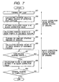
- the flow chart shown in Fig. 7 includes two parts, one is a process of setting a black offset correction value to be executed before an original read operation, and the other is a process of updating (changing) a black offset correction value to be executed during an original read operation.
- Fig. 6 shows an sample of an image signal of one line (during 1H).
- an image signal (indicated by a broken line in Fig. 6 ) while a lamp is turned off is used.
- a signal during a blanking period (during a non-image period) is used.
- Step 801 the lamp is turned off.
- each of the adder circuits 509 to 512 calculates an average value B of image signals, of effective pixels. This average value B of pixel signals in this lamp turn-off state is set as a black offset correction value at Step 803.
- Step 804 an average value K of pixel signals from a non-image pixel portion of each respective sub-array of pixels is calculated by the respective adder circuits 509 to 512.
- Step 805 the lamp is turned on to allow the image input apparatus to start reading an original and acquire image information.
- a respective average value RK of the pixel signals is calculated by the respective adder circuits 509 to 512.
- Step 807 it is checked whether the period is a non-original reading period (a period from the end of reading one original to the start of reading another original). If during the non-original reading period, at Step 808 each of the black value offset setting registers 517 to 520 updates (changes) the black correction value to correct any change in the black correction value during reading the previous original and prevent a change in the image quality caused by such change.
- the updated black correction value is "B + (RK-K)" which cancels out an offset fluctuation changing every moment.
- the black offset of an image signal can be corrected reliably by updating (changing) the black correction value by using signals output during the non-image pixel period.
- a precision of black correction may be lowered more or less because a signal from the black reference pixel portion contains, in many cases, clamp pulse noises (such as crosstalk from a clamp pulse) generated in an analog circuit such as a clamp circuit at the stage before the AD converters. If clamp pulse noises are not contained, a signal from the black reference pixel can be used for black correction at a high precision, similar to a signal from the non-image pixel portion.
- clamp pulse noises such as crosstalk from a clamp pulse
- a background example will be described.
- a method of calculating an updated value for updating (changing) the black correction value is different from the invention .
- the other structure and operation are same as the invention.
- Fig. 8 is a flow chart illustrating the operation of an image input apparatus of this example.
- the updated value for updating (changing) the black correction value is set at Step 808 by using a difference between the average value RK of pixel signals in the non-image pixel portion in the lamp turn-on state and the average value K in the non-image pixel portion in the lamp turn-off state.
- the updated value for updating (changing) the black correction value is set at Step 908 by using a difference between the average value RK of pixel signals in the non-image pixel portion in the lamp turn-on state and an average value of RK values of the non-image pixel portion of four channels in the lamp turn-on state.
- correcting means corrects an offset component by adjusting a fluctuation of the offset component contained in a signal output from photoelectric conversion means during picking up image information of an object.
- the present invention can be implemented by applying the image input apparatus with a storage medium storing software program codes realizing the functions of the invention described above, and by reading and executing the programs codes stored in the storage medium by a computer (CPU or MPU) of the image input apparatus.
- a computer CPU or MPU
- the program codes themselves read from the storage medium realize the functions of each embodiment. Therefore, the storage medium storing such program codes constitutes the present invention.
- the storage medium for storing such program codes may be a floppy disk, a hard disk, an optical disk, a magnetooptical disk, a CD-ROM, a CD-R, a magnetic tape, a nonvolatile memory card, a ROM or the like.
- the functions of of the invention can be realized by executing the program codes read by a computer, but also the case wherein the functions of the invention can be realized by executing a portion or the whole of processes by an OS running on the computer, in accordance with the program codes.
- the functions of the invention can be realized by writing the program codes read from the storage medium into a memory of a function expansion board inserted into a computer or of a function expansion unit connected to the computer, and thereafter by executing a portion or the whole of actual processes by a CPU of the function expansion board or function expansion unit.
- the invention provides an image input system using an image input apparatus as described above.
- reference numeral 201 represents an original support glass
- reference numeral 202 represents an original
- reference numeral 203 represents an illumination lamp for illuminating an original.
- Reference numeral 207 represents a lens for focussing an original image on a light receiving surface of the linear image sensor 208 of one of the first to fifth embodiments.
- Reference numerals 204 to 205 represent first to third mirrors for guiding light reflected from the original to the lens 207.
- Reference numeral 209 represents a white board which is read as a reference of the shading correction process.
- Reference numeral 210 represents a dummy glass for making the optical distance from the linear image sensor 208 to the white board surface equal to that to the original surface.
- the mirrors move in the sub-scan direction so that the original can be read two-dimensionally.
Landscapes
- Engineering & Computer Science (AREA)
- Multimedia (AREA)
- Signal Processing (AREA)
- Facsimile Image Signal Circuits (AREA)
- Facsimile Scanning Arrangements (AREA)
- Transforming Light Signals Into Electric Signals (AREA)
Claims (7)
- Bildeingabevorrichtung, mit:einer photoelektrischen Umwandlungseinheit (208), die dazu angepasst ist, Bildinformationen eines Objekts zu beschaffen und entsprechende Signale von jeder einer Vielzahl von Ausgabeeinheiten (302 - 305) auszugeben, wobei die photoelektrische Umwandlungseinheit einen Effektivpixelabschnitt und einen Nichtabbildungspixelabschnitt, der von dem Effektivpixelabschnitt verschieden ist, umfasst; undeiner Korrektureinheit (513 - 516), die dazu angepasst ist, die Ausgabesignale, die von jeder der Ausgabeeinheiten während einer Periode des Beschaffens der Bildinformationen ausgegeben werden, basierend auf einem Schwarzkorrekturwert zu korrigieren, undeiner Einstelleinheit (526), die dazu angepasst ist, den Schwarzkorrekturwert basierend auf einem ersten Mittelwert B von Pixelsignalen einzustellen und den Schwarzkorrekturwert basierend auf einer Differenz zwischen einem zweiten Mittelwert K von Pixelsignalen und einem dritten Mittelwert RK von Pixelsignalen zu aktualisieren,wobeider erste Mittelwert B von Pixelsignalen aus Ausgabesignalen von dem Effektivpixelabschnitt berechnet wird, bevor das Objekt gelesen wird,der zweite Mittelwert K von Pixelsignalen aus Ausgabesignalen von dem Nichtabbildungspixelabschnitt berechnet wird, bevor das Objekt gelesen wird, undder dritte Mittelwert RK von Pixelsignalen aus Ausgabesignalen von dem Nichtabbildungspixelabschnitt berechnet wird, während das Objekt gelesen wird.
- Bildeingabevorrichtung gemäß Anspruch 1, wobei die photoelektrische Umwandlungseinheit einen linearen Bildsensor aufweist und jede der Ausgabeeinheiten ein Signal von einem unterschiedlichen Pixel in dem linearen Bildsensor ausgibt.
- Bildeingabevorrichtung gemäß einem der vorstehenden Ansprüche, wobei die Korrektureinheit dazu angepasst ist, den Schwarzkorrekturwert von Signalen, die von der photoelektrischen Umwandlungseinheit während der Periode des Beschaffens der Bildinformationen ausgegeben werden, zu subtrahieren, und
die Einstelleinheit umfasst:eine Berechnungseinheit, die dazu angepasst ist, eine Differenz zwischen den zweiten und dritten Mittelwerten zu berechnen; undeine Anpasseinheit (526), die dazu angepasst ist, den ersten Mittelwert unter Verwendung der Differenz anzupassen. - Bildeingabevorrichtung gemäß Anspruch 3, wobei das Anpassen des ersten Mittelwerts durch die Anpasseinheit (526) während einer anderen Periode als einer Periode des Beschaffens von Bildinformationen ausgeführt wird.
- Bildverarbeitungsverfahren des Verarbeitens von Signalen, die von einer photoelektrischen Umwandlungseinheit (208) ausgegeben werden, die dazu angepasst ist, Bildinformationen eines Objekts (202) zu beschaffen und die entsprechenden Signale von jeder einer Vielzahl von Ausgabeeinheiten (302 - 305) auszugeben, wobei die photoelektrische Umwandlungseinheit einen Effektivpixelabschnitt und einen Nichtabbildungspixelabschnitt, der von dem Effektivpixelabschnitt verschieden ist, umfasst, wobei das Verfahren aufweist:Korrigieren der Ausgabesignale, die von jeder der Ausgabeeinheiten während einer Periode des Beschaffens der Bildinformationen ausgegeben werden, basierend auf einem Schwarzkorrekturwert, undEinstellen des Schwarzkorrekturwerts basierend auf einem ersten Mittelwert B von Pixelsignalen einzustellen und Aktualisieren des Schwarzkorrekturwerts basierend auf einer Differenz zwischen einem zweiten Mittelwert K von Pixelsignalen und einem dritten Mittelwert RK von Pixelsignalen,wobeider erste Mittelwert B von Pixelsignalen aus Ausgabesignalen von dem Effektivpixelabschnitt berechnet wird, bevor das Objekt gelesen wird,der zweite Mittelwert K von Pixelsignalen aus Ausgabesignalen von dem Nichtabbildungspixelabschnitt berechnet wird, bevor das Objekt gelesen wird, undder dritte Mittelwert RK von Pixelsignalen aus Ausgabesignalen von dem Nichtabbildungspixelabschnitt berechnet wird, während das Objekt gelesen wird.
- Computer-lesbares Speichermedium mit darauf gespeichertem Computerprogrammcode, der dazu angepasst ist, eine Bildverarbeitung gemäß dem Bildverarbeitungsverfahren nach Anspruch 5 auszuführen.
- Bildeingabesystem, mit:einer Vorlagenhalterung (201), um eine Vorlage (202) darauf zu platzieren;eine Beleuchtungslampe (203) zum Beleuchten einer Vorlage, die auf der Vorlagenhalterung platziert ist;der Bildeingabevorrichtung gemäß einem der Ansprüche 1 bis 4;einer Linse (207) zum Fokussieren von Licht das von der mit der Beleuchtungslampe beleuchteten Vorlage auf der Bildeingabevorrichtung reflektiert wird; undeine Vielzahl von Spiegeln (204 - 206) zum Führen des von der Vorlage reflektierten Lichts zu der Linse.
Applications Claiming Priority (4)
| Application Number | Priority Date | Filing Date | Title |
|---|---|---|---|
| JP23246399A JP3792956B2 (ja) | 1999-08-19 | 1999-08-19 | 画像入力装置及びそれを用いた画像入力システム |
| JP23246399 | 1999-08-19 | ||
| JP2000016949A JP2001211297A (ja) | 2000-01-26 | 2000-01-26 | 画像読み取り装置、方法及び記憶媒体 |
| JP2000016949 | 2000-01-26 |
Publications (3)
| Publication Number | Publication Date |
|---|---|
| EP1079602A2 EP1079602A2 (de) | 2001-02-28 |
| EP1079602A3 EP1079602A3 (de) | 2004-07-07 |
| EP1079602B1 true EP1079602B1 (de) | 2013-10-16 |
Family
ID=26530480
Family Applications (1)
| Application Number | Title | Priority Date | Filing Date |
|---|---|---|---|
| EP00307097.6A Expired - Lifetime EP1079602B1 (de) | 1999-08-19 | 2000-08-18 | Bildeingabevorrichtung |
Country Status (2)
| Country | Link |
|---|---|
| US (2) | US7053941B1 (de) |
| EP (1) | EP1079602B1 (de) |
Families Citing this family (8)
| Publication number | Priority date | Publication date | Assignee | Title |
|---|---|---|---|---|
| US7050098B2 (en) | 2001-03-29 | 2006-05-23 | Canon Kabushiki Kaisha | Signal processing apparatus and method, and image sensing apparatus having a plurality of image sensing regions per image frame |
| DE10242516A1 (de) * | 2002-09-12 | 2004-03-25 | Bts Media Solutions Gmbh | Verfahren und Anordnung zur Korrektur von Videosignalen |
| AU2004249063B2 (en) * | 2003-06-24 | 2008-12-11 | Olympus Corporation | Encapsulated endoscope and encapsulated endoscope system |
| JP4340503B2 (ja) * | 2003-09-18 | 2009-10-07 | 株式会社リコー | 原稿読取装置 |
| US7385636B2 (en) * | 2004-04-30 | 2008-06-10 | Eastman Kodak Company | Low noise sample and hold circuit for image sensors |
| JP4424753B2 (ja) * | 2007-12-28 | 2010-03-03 | キヤノン株式会社 | 固体撮像装置及びその駆動方法 |
| JP5262744B2 (ja) * | 2009-01-20 | 2013-08-14 | 富士ゼロックス株式会社 | 画像読取装置、黒補正実行判定プログラム |
| JP7508391B2 (ja) * | 2021-03-10 | 2024-07-01 | 株式会社東芝 | 固体撮像装置、固体撮像装置の駆動方法 |
Family Cites Families (30)
| Publication number | Priority date | Publication date | Assignee | Title |
|---|---|---|---|---|
| JPS6352575A (ja) | 1986-08-22 | 1988-03-05 | Matsushita Electric Ind Co Ltd | シエ−デイング補正装置 |
| US5233414A (en) | 1987-12-08 | 1993-08-03 | Canon Kabushiki Kaisha | Color image processing apparatus |
| JPH0787532B2 (ja) * | 1988-08-24 | 1995-09-20 | 富士写真フイルム株式会社 | 画像情報読取装置のシェーディング補正方法 |
| US5267053A (en) | 1988-10-27 | 1993-11-30 | Eastman Kodak Company | Automatic reference control for image scanners |
| JPH02148972A (ja) | 1988-11-29 | 1990-06-07 | Fuji Photo Film Co Ltd | 画像信号補正方法および装置 |
| JPH04113766A (ja) | 1990-09-04 | 1992-04-15 | Canon Inc | 固体撮像装置 |
| JPH04271678A (ja) | 1991-02-27 | 1992-09-28 | Sony Corp | 固体撮像素子 |
| JP3192441B2 (ja) | 1991-07-11 | 2001-07-30 | 株式会社リコー | 画像読取装置 |
| US5289286A (en) * | 1991-07-18 | 1994-02-22 | Minolta Camera Kabushiki Kaisha | Solid state sensor having logarithmic photovoltaic response, with pixel uniformity correction and white balance circuitry therefor |
| JPH05227427A (ja) | 1992-02-10 | 1993-09-03 | N T T Data Tsushin Kk | シェ−ディング補正システム |
| JPH05292242A (ja) | 1992-04-06 | 1993-11-05 | Sony Corp | 電荷転送装置 |
| JPH05328039A (ja) | 1992-05-25 | 1993-12-10 | Ricoh Co Ltd | 画像読取装置 |
| JP3241882B2 (ja) | 1993-07-08 | 2001-12-25 | ソニー株式会社 | 固体撮像装置 |
| JPH0738814A (ja) | 1993-07-21 | 1995-02-07 | Fujitsu Ltd | 固体撮像装置 |
| JP3494462B2 (ja) | 1993-12-28 | 2004-02-09 | 株式会社東芝 | 信号処理装置 |
| KR0136067B1 (ko) | 1994-08-12 | 1998-04-27 | 김광호 | 이치화상 프로세서 |
| US5659355A (en) * | 1994-10-31 | 1997-08-19 | Eastman Kodak Company | CCD dark mean level correction circuit employing digital processing and analog subtraction requiring no advance knowledge of dark mean level |
| US5917620A (en) | 1995-03-07 | 1999-06-29 | Canon Kabushiki Kaisha | Image reading apparatus |
| JPH0951410A (ja) | 1995-05-26 | 1997-02-18 | Minolta Co Ltd | フィルム画像読取装置 |
| JP3612803B2 (ja) | 1995-07-10 | 2005-01-19 | ソニー株式会社 | 固体撮像装置及び固体撮像素子の出力信号処理方法 |
| JPH0937040A (ja) | 1995-07-24 | 1997-02-07 | Canon Inc | 画像走査装置 |
| JPH09200605A (ja) | 1996-01-12 | 1997-07-31 | Sanyo Electric Co Ltd | ディジタルビデオカメラ |
| JPH09298647A (ja) | 1996-05-01 | 1997-11-18 | Fuji Photo Film Co Ltd | リニアイメージセンサのオフセットレベル補正方法およびその装置 |
| JP3804113B2 (ja) | 1996-08-26 | 2006-08-02 | コニカミノルタホールディングス株式会社 | 固体撮像装置 |
| JP3466855B2 (ja) * | 1997-02-07 | 2003-11-17 | 株式会社リコー | 画像読取装置 |
| JP3574563B2 (ja) | 1997-04-04 | 2004-10-06 | ペンタックス株式会社 | 画素信号処理装置 |
| US6337713B1 (en) | 1997-04-04 | 2002-01-08 | Asahi Kogaku Kogyo Kabushiki Kaisha | Processor for image-pixel signals derived from divided sections of image-sensing area of solid-type image sensor |
| US6330083B1 (en) * | 1997-05-28 | 2001-12-11 | Minolta Co., Ltd. | Image reading device performing light quantity detection and correction with timing corresponding to selected copying mode |
| JP3940489B2 (ja) | 1998-03-13 | 2007-07-04 | 株式会社東芝 | 画像読み取り装置及び方法 |
| JPH11289432A (ja) | 1998-04-03 | 1999-10-19 | Mita Ind Co Ltd | デジタル画像読取装置 |
-
2000
- 2000-08-16 US US09/639,082 patent/US7053941B1/en not_active Expired - Fee Related
- 2000-08-18 EP EP00307097.6A patent/EP1079602B1/de not_active Expired - Lifetime
-
2005
- 2005-09-26 US US11/234,099 patent/US7542081B2/en not_active Expired - Fee Related
Also Published As
| Publication number | Publication date |
|---|---|
| US7542081B2 (en) | 2009-06-02 |
| EP1079602A2 (de) | 2001-02-28 |
| US7053941B1 (en) | 2006-05-30 |
| EP1079602A3 (de) | 2004-07-07 |
| US20060017819A1 (en) | 2006-01-26 |
Similar Documents
| Publication | Publication Date | Title |
|---|---|---|
| US7477302B2 (en) | Solid-state image pickup apparatus and image pickup method | |
| US7679658B2 (en) | Solid-state image pickup apparatus | |
| US9800809B2 (en) | Imaging apparatus, imaging system, and method for reducing a difference in resolutions | |
| EP1137255B1 (de) | Korrekturverfahren und -vorrichtung für Bildsignale die durch einen Bildsensor mit mehreren Ausgangskanälen erzeugt wurden | |
| JP3809226B2 (ja) | リニアイメージセンサの出力画像信号の補正方法 | |
| US20050243193A1 (en) | Suppression of row-wise noise in an imager | |
| US20080054320A1 (en) | Method, apparatus and system providing suppression of noise in a digital imager | |
| EP2161919B1 (de) | Ableseverfahren für eine CMOS-Bildgebungsvorrichtung mit verringertem Dunkelstrom | |
| EP1079602B1 (de) | Bildeingabevorrichtung | |
| JPH04363967A (ja) | 原稿読取り装置 | |
| US7869086B2 (en) | Offset adjusting device, correcting device, and method of adjusting analog image signal | |
| US5940125A (en) | Correcting offset level using a proportional distribution of a difference in dark current levels in a line image sensor | |
| US6445413B1 (en) | System for determining a video offset from dark photosensors in an image sensor array | |
| US6853402B2 (en) | Combined multiplexing and offset correction for an image sensor array | |
| JP3879571B2 (ja) | 撮像装置 | |
| EP0848546A1 (de) | Festkörper-Bildaufnahmeanordnung und Steuerverfahren dafür | |
| JP2021110885A (ja) | 撮像装置及びその制御方法 | |
| JP2010093759A (ja) | 撮像センサ及び撮像装置 | |
| JP3792956B2 (ja) | 画像入力装置及びそれを用いた画像入力システム | |
| EP0808057B1 (de) | Verfahren und Vorrichtung zum Korrigieren eines Ausgangssignals eines Zeilensensors | |
| JP2001346012A (ja) | 画像読取装置及び画像信号の調整方法 | |
| JP4101192B2 (ja) | 画像読取装置及び画像処理装置 | |
| JP2020129755A (ja) | 画像処理装及び方法、及び撮像装置 | |
| EP0542267B1 (de) | Korrekturschaltung für Bildabtaster | |
| JP4303875B2 (ja) | 固体撮像装置 |
Legal Events
| Date | Code | Title | Description |
|---|---|---|---|
| PUAI | Public reference made under article 153(3) epc to a published international application that has entered the european phase |
Free format text: ORIGINAL CODE: 0009012 |
|
| AK | Designated contracting states |
Kind code of ref document: A2 Designated state(s): AT BE CH CY DE DK ES FI FR GB GR IE IT LI LU MC NL PT SE |
|
| AX | Request for extension of the european patent |
Free format text: AL;LT;LV;MK;RO;SI |
|
| RIC1 | Information provided on ipc code assigned before grant |
Ipc: 7H 04N 9/04 B Ipc: 7H 04N 5/335 B Ipc: 7H 04N 5/217 B Ipc: 7H 04N 1/401 B Ipc: 7H 04N 1/40 B Ipc: 7H 04N 1/46 B Ipc: 7H 04N 3/15 B Ipc: 7H 04N 1/04 B Ipc: 7H 04N 1/407 A |
|
| PUAL | Search report despatched |
Free format text: ORIGINAL CODE: 0009013 |
|
| AK | Designated contracting states |
Kind code of ref document: A3 Designated state(s): AT BE CH CY DE DK ES FI FR GB GR IE IT LI LU MC NL PT SE |
|
| AX | Request for extension of the european patent |
Extension state: AL LT LV MK RO SI |
|
| 17P | Request for examination filed |
Effective date: 20041122 |
|
| 17Q | First examination report despatched |
Effective date: 20041228 |
|
| AKX | Designation fees paid |
Designated state(s): DE FR GB IT |
|
| 17Q | First examination report despatched |
Effective date: 20041228 |
|
| GRAP | Despatch of communication of intention to grant a patent |
Free format text: ORIGINAL CODE: EPIDOSNIGR1 |
|
| GRAS | Grant fee paid |
Free format text: ORIGINAL CODE: EPIDOSNIGR3 |
|
| RIC1 | Information provided on ipc code assigned before grant |
Ipc: H04N 1/04 20060101ALI20130613BHEP Ipc: H04N 9/04 20060101ALI20130613BHEP Ipc: H04N 1/40 20060101ALI20130613BHEP Ipc: H04N 5/335 20110101ALI20130613BHEP Ipc: H04N 5/217 20110101ALI20130613BHEP Ipc: H04N 1/407 20060101AFI20130613BHEP Ipc: H04N 1/401 20060101ALI20130613BHEP |
|
| GRAA | (expected) grant |
Free format text: ORIGINAL CODE: 0009210 |
|
| AK | Designated contracting states |
Kind code of ref document: B1 Designated state(s): DE FR GB IT |
|
| REG | Reference to a national code |
Ref country code: GB Ref legal event code: FG4D |
|
| REG | Reference to a national code |
Ref country code: DE Ref legal event code: R096 Ref document number: 60048297 Country of ref document: DE Effective date: 20131212 |
|
| REG | Reference to a national code |
Ref country code: DE Ref legal event code: R097 Ref document number: 60048297 Country of ref document: DE |
|
| PLBE | No opposition filed within time limit |
Free format text: ORIGINAL CODE: 0009261 |
|
| STAA | Information on the status of an ep patent application or granted ep patent |
Free format text: STATUS: NO OPPOSITION FILED WITHIN TIME LIMIT |
|
| PG25 | Lapsed in a contracting state [announced via postgrant information from national office to epo] |
Ref country code: IT Free format text: LAPSE BECAUSE OF FAILURE TO SUBMIT A TRANSLATION OF THE DESCRIPTION OR TO PAY THE FEE WITHIN THE PRESCRIBED TIME-LIMIT Effective date: 20131016 |
|
| 26N | No opposition filed |
Effective date: 20140717 |
|
| REG | Reference to a national code |
Ref country code: DE Ref legal event code: R097 Ref document number: 60048297 Country of ref document: DE Effective date: 20140717 |
|
| REG | Reference to a national code |
Ref country code: DE Ref legal event code: R119 Ref document number: 60048297 Country of ref document: DE |
|
| GBPC | Gb: european patent ceased through non-payment of renewal fee |
Effective date: 20140818 |
|
| REG | Reference to a national code |
Ref country code: DE Ref legal event code: R119 Ref document number: 60048297 Country of ref document: DE Effective date: 20150303 |
|
| REG | Reference to a national code |
Ref country code: FR Ref legal event code: ST Effective date: 20150430 |
|
| PG25 | Lapsed in a contracting state [announced via postgrant information from national office to epo] |
Ref country code: GB Free format text: LAPSE BECAUSE OF NON-PAYMENT OF DUE FEES Effective date: 20140818 Ref country code: DE Free format text: LAPSE BECAUSE OF NON-PAYMENT OF DUE FEES Effective date: 20150303 |
|
| PG25 | Lapsed in a contracting state [announced via postgrant information from national office to epo] |
Ref country code: FR Free format text: LAPSE BECAUSE OF NON-PAYMENT OF DUE FEES Effective date: 20140901 |