EP1079602B1 - Image input apparatus - Google Patents
Image input apparatus Download PDFInfo
- Publication number
- EP1079602B1 EP1079602B1 EP00307097.6A EP00307097A EP1079602B1 EP 1079602 B1 EP1079602 B1 EP 1079602B1 EP 00307097 A EP00307097 A EP 00307097A EP 1079602 B1 EP1079602 B1 EP 1079602B1
- Authority
- EP
- European Patent Office
- Prior art keywords
- image
- signals
- output
- pixel
- average value
- Prior art date
- Legal status (The legal status is an assumption and is not a legal conclusion. Google has not performed a legal analysis and makes no representation as to the accuracy of the status listed.)
- Expired - Lifetime
Links
Images


Classifications
-
- H—ELECTRICITY
- H04—ELECTRIC COMMUNICATION TECHNIQUE
- H04N—PICTORIAL COMMUNICATION, e.g. TELEVISION
- H04N1/00—Scanning, transmission or reproduction of documents or the like, e.g. facsimile transmission; Details thereof
- H04N1/40—Picture signal circuits
- H04N1/407—Control or modification of tonal gradation or of extreme levels, e.g. background level
-
- H—ELECTRICITY
- H04—ELECTRIC COMMUNICATION TECHNIQUE
- H04N—PICTORIAL COMMUNICATION, e.g. TELEVISION
- H04N1/00—Scanning, transmission or reproduction of documents or the like, e.g. facsimile transmission; Details thereof
- H04N1/40—Picture signal circuits
- H04N1/401—Compensating positionally unequal response of the pick-up or reproducing head
Definitions
- the present invention relates to an image input apparatus for forming image information of an object by photoelectric conversion, a correcting unit for use therein, an image input system, including such an apparatus, a method of image processing and a computer readable storage medium for implementing such a method.
- An image input apparatus using a linear image sensor is known.
- Fig. 1 shows the structure of a linear CCD image sensor used in a conventional image input apparatus.
- reference numeral 101 represents a light receiving pixel array of a linear CCD image sensor.
- Reference numeral 102 represents an analog shift register for sequentially reading electric charges accumulated in odd pixels of the pixel array
- reference numeral 103 represents an analog shift register for sequentially reading electric charges accumulated in even pixels of the pixel array.
- Reference numerals 104 and 105 represent output amplifiers for converting the electric charges read by the analog shift registers 102 and 103 into voltage signals.
- Electric charges of the pixel array 101 of the linear CCD image sensor shown in Fig. 1 are read by grouping the pixels into even and odd pixels, in order to obtain a read speed higher than a predetermined speed, because the analog shift registers 102 and 103 have a limit in the transfer speed.
- An image input apparatus having a read speed higher than that of a conventional linear CCD image sensor of an even/odd separation read type such as shown in Fig. 1 has been desired.
- a linear CCD image sensor capable of realizing a read speed two times as fast as that of a linear CCD image sensor of an odd/even separation read type has been proposed. As shown in Fig. 3 , this linear CCD image sensor has a right/left division read structure in addition to an even/odd separation read structure.
- the linear CCD image sensor shown in Fig. 3 has four analog shift registers 302 to 305 to read electric charges from a light receiving pixel array by dividing them into right and left pixels and grouping each of the right and left pixels into even and odd pixels.
- the linear CCD image sensor of the right/left division type shown in Fig. 3 is, however, associated with the following problem.
- a level of each of the read signals of right/left four channels becomes different at the boundary between the right and left pixels if an offset of read signal of each channel has a different offset level.
- Document US 5 917 620 A discloses an image reading apparatus comprising plural line sensors for converting light from an object into image signals, charge transfer unit for transferring the image signals, converted by the line sensors, mutually among the line sensors, correction unit for correcting signal levels of the image signals and control unit for effecting control so as to vary a manner of correction by the correction unit, according to a direction of transfer of the image signals by the charge transfer means among the line sensors.
- the image input apparatus of the present invention is intended to correct offset components contained in signals and obtain an image of good quality.
- an image input apparatus as defined in claim 1.
- an image processing method as defined in claim 5 there is provided an image processing method as defined in claim 5.
- Fig. 3 is a diagram showing the structure of a linear CCD image sensor 208 of a right/left division read type to be used as photoelectric conversion means.
- reference numeral 301 represents a light receiving pixel array or arrangement.
- Reference numerals 302, 303, 304 and 305 represent an analog shift register (reading means).
- Reference numerals 306, 307, 308 and 309 represent an output amplifier for converting electric charges read from each of the analog shift registers 302 to 305 into a voltage signal.
- This image sensor 208 reads electric charges by dividing pixels into even and odd pixels and by dividing the light receiving pixel array 301 of the image sensor 208 into right and left pixel subarrays 301R and 301L at the halfway position of the array 301.
- Electric charges accumulated in the left pixel subarray 301L are output from the output amplifier 306 for odd pixels and from the output amplifier 308 for even pixels, respectively as pixel signals ODD-1 and EVEN-1.
- electric charges accumulated in the right pixel subarray 301R are output from the output amplifier 307 for odd pixels and from the output amplifier 309 for even pixels, respectively as pixel signals ODD-2 and EVEN-2.
- Fig. 5 is a block diagram showing the structure of a signal processing unit of the image input apparatus.
- reference numerals 501 to 504 represent an amplifier for amplifying each output of the linear CCD image sensor of the right/left division read type used as photoelectric conversion means shown in Fig. 3 .
- Reference numerals 505 to 508 represent an AD converter for converting an output of each of the output amplifiers 501 to 504 into a digital signal.
- Reference numerals 509 to 512 represent an adder circuit used as adding means for adding image signals of each channel during an optional period.
- Reference numerals 513 to 516 represent a subtractor circuit used as subtracting means for subtracting a black offset component from an image signal of each channel.
- Reference numerals 517 to 520 represent a black correction value setting register used for adjusting means for setting the black offset component.
- Reference numerals 521 to 524 represent a shading correction circuit for executing a shading correction process of the image signal of each channel.
- Reference numeral 525 represents a memory circuit used for rearranging the order (shown in Fig. 4 ) of image signals output from the linear CCD image sensor of the right/left division read type into a predetermined order.
- Reference numeral 526 represents a CPU for controlling the adder circuits, black correction value setting registers and the like.
- the adder circuits, subtractor circuits and black correction value setting registers constitute correcting means for correcting an offset component by adjusting a fluctuation of the offset component contained in each image signal output of the linear CCD image sensor.
- the offset component fluctuation occurs whole image information of an object such as an original is picked up.
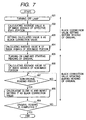
- the flow chart shown in Fig. 7 includes two parts, one is a process of setting a black offset correction value to be executed before an original read operation, and the other is a process of updating (changing) a black offset correction value to be executed during an original read operation.
- Fig. 6 shows an sample of an image signal of one line (during 1H).
- an image signal (indicated by a broken line in Fig. 6 ) while a lamp is turned off is used.
- a signal during a blanking period (during a non-image period) is used.
- Step 801 the lamp is turned off.
- each of the adder circuits 509 to 512 calculates an average value B of image signals, of effective pixels. This average value B of pixel signals in this lamp turn-off state is set as a black offset correction value at Step 803.
- Step 804 an average value K of pixel signals from a non-image pixel portion of each respective sub-array of pixels is calculated by the respective adder circuits 509 to 512.
- Step 805 the lamp is turned on to allow the image input apparatus to start reading an original and acquire image information.
- a respective average value RK of the pixel signals is calculated by the respective adder circuits 509 to 512.
- Step 807 it is checked whether the period is a non-original reading period (a period from the end of reading one original to the start of reading another original). If during the non-original reading period, at Step 808 each of the black value offset setting registers 517 to 520 updates (changes) the black correction value to correct any change in the black correction value during reading the previous original and prevent a change in the image quality caused by such change.
- the updated black correction value is "B + (RK-K)" which cancels out an offset fluctuation changing every moment.
- the black offset of an image signal can be corrected reliably by updating (changing) the black correction value by using signals output during the non-image pixel period.
- a precision of black correction may be lowered more or less because a signal from the black reference pixel portion contains, in many cases, clamp pulse noises (such as crosstalk from a clamp pulse) generated in an analog circuit such as a clamp circuit at the stage before the AD converters. If clamp pulse noises are not contained, a signal from the black reference pixel can be used for black correction at a high precision, similar to a signal from the non-image pixel portion.
- clamp pulse noises such as crosstalk from a clamp pulse
- a background example will be described.
- a method of calculating an updated value for updating (changing) the black correction value is different from the invention .
- the other structure and operation are same as the invention.
- Fig. 8 is a flow chart illustrating the operation of an image input apparatus of this example.
- the updated value for updating (changing) the black correction value is set at Step 808 by using a difference between the average value RK of pixel signals in the non-image pixel portion in the lamp turn-on state and the average value K in the non-image pixel portion in the lamp turn-off state.
- the updated value for updating (changing) the black correction value is set at Step 908 by using a difference between the average value RK of pixel signals in the non-image pixel portion in the lamp turn-on state and an average value of RK values of the non-image pixel portion of four channels in the lamp turn-on state.
- correcting means corrects an offset component by adjusting a fluctuation of the offset component contained in a signal output from photoelectric conversion means during picking up image information of an object.
- the present invention can be implemented by applying the image input apparatus with a storage medium storing software program codes realizing the functions of the invention described above, and by reading and executing the programs codes stored in the storage medium by a computer (CPU or MPU) of the image input apparatus.
- a computer CPU or MPU
- the program codes themselves read from the storage medium realize the functions of each embodiment. Therefore, the storage medium storing such program codes constitutes the present invention.
- the storage medium for storing such program codes may be a floppy disk, a hard disk, an optical disk, a magnetooptical disk, a CD-ROM, a CD-R, a magnetic tape, a nonvolatile memory card, a ROM or the like.
- the functions of of the invention can be realized by executing the program codes read by a computer, but also the case wherein the functions of the invention can be realized by executing a portion or the whole of processes by an OS running on the computer, in accordance with the program codes.
- the functions of the invention can be realized by writing the program codes read from the storage medium into a memory of a function expansion board inserted into a computer or of a function expansion unit connected to the computer, and thereafter by executing a portion or the whole of actual processes by a CPU of the function expansion board or function expansion unit.
- the invention provides an image input system using an image input apparatus as described above.
- reference numeral 201 represents an original support glass
- reference numeral 202 represents an original
- reference numeral 203 represents an illumination lamp for illuminating an original.
- Reference numeral 207 represents a lens for focussing an original image on a light receiving surface of the linear image sensor 208 of one of the first to fifth embodiments.
- Reference numerals 204 to 205 represent first to third mirrors for guiding light reflected from the original to the lens 207.
- Reference numeral 209 represents a white board which is read as a reference of the shading correction process.
- Reference numeral 210 represents a dummy glass for making the optical distance from the linear image sensor 208 to the white board surface equal to that to the original surface.
- the mirrors move in the sub-scan direction so that the original can be read two-dimensionally.
Description
- The present invention relates to an image input apparatus for forming image information of an object by photoelectric conversion, a correcting unit for use therein, an image input system, including such an apparatus, a method of image processing and a computer readable storage medium for implementing such a method.
- An image input apparatus using a linear image sensor is known.
-
Fig. 1 shows the structure of a linear CCD image sensor used in a conventional image input apparatus. - In
Fig. 1 ,reference numeral 101 represents a light receiving pixel array of a linear CCD image sensor.Reference numeral 102 represents an analog shift register for sequentially reading electric charges accumulated in odd pixels of the pixel array, andreference numeral 103 represents an analog shift register for sequentially reading electric charges accumulated in even pixels of the pixel array.Reference numerals analog shift registers - Electric charges of the
pixel array 101 of the linear CCD image sensor shown inFig. 1 are read by grouping the pixels into even and odd pixels, in order to obtain a read speed higher than a predetermined speed, because theanalog shift registers - An image input apparatus having a read speed higher than that of a conventional linear CCD image sensor of an even/odd separation read type such as shown in
Fig. 1 has been desired. - A linear CCD image sensor capable of realizing a read speed two times as fast as that of a linear CCD image sensor of an odd/even separation read type has been proposed. As shown in
Fig. 3 , this linear CCD image sensor has a right/left division read structure in addition to an even/odd separation read structure. - The linear CCD image sensor shown in
Fig. 3 has fouranalog shift registers 302 to 305 to read electric charges from a light receiving pixel array by dividing them into right and left pixels and grouping each of the right and left pixels into even and odd pixels. - The linear CCD image sensor of the right/left division type shown in
Fig. 3 is, however, associated with the following problem. - A level of each of the read signals of right/left four channels becomes different at the boundary between the right and left pixels if an offset of read signal of each channel has a different offset level.
- In a conventional linear CCD image sensor of the even/odd separation read type, even if there is a signal level difference between even/odd pixels, only a very fine repetitive pattern appears on an image. However, in a linear CCD image sensor of the right/left division read type, even if difference between a read signal levels of the four channels is very small, a visually conspicuous line appears on an image at the right/left boundary.
- Such offset levels can be corrected by proper means.
- Such correction is performed once prior to reading an original, and thus the following problem occurs. An offset level fluctuates during the original read operation because of temperature change in a CCD sensor, analog circuits, video circuits and the like. Therefore, the read signal level fluctuates as shown in
Fig. 2 . This fluctuation causes clear difference in a signal level between the right and left images picked up with an image input apparatus using a linear CCD image sensor of the right/left division read type. - Document
US 5 917 620 A discloses an image reading apparatus comprising plural line sensors for converting light from an object into image signals, charge transfer unit for transferring the image signals, converted by the line sensors, mutually among the line sensors, correction unit for correcting signal levels of the image signals and control unit for effecting control so as to vary a manner of correction by the correction unit, according to a direction of transfer of the image signals by the charge transfer means among the line sensors. - The image input apparatus of the present invention is intended to correct offset components contained in signals and obtain an image of good quality.
- According to an aspect of the present invention, there is provided an image input apparatus as defined in
claim 1. - According to another aspect of the present invention, there is provided an image processing method as defined in
claim 5. - According to still another aspect of the present invention, there is provided a system as defined in claim 7.
- Further aspects and features of the invention are set out in the dependent claims.
- The features of this invention will become apparent from the following detailed description of embodiments when read in conjunction with the accompanying drawings wherein:
-
Fig. 1 is a diagram showing a conventional CCD sensor; -
Fig. 2 is a graph illustrating a problem associated with conventional techniques; -
Fig. 3 is a diagram showing a right/left division read type CCD sensor used by the invention; -
Fig. 4 is a diagram showing image signals output from a right/left division read type CCD sensor ; -
Fig. 5 is a diagram showing the structure of a processing unit according to the invention; -
Fig. 6 is a diagram showing an image signal illustrating the invention; -
Fig. 7 is a flow chart illustrating the operation of the image input apparatus according to the invention ; -
Fig. 8 is a flow chart illustrating the operation of the image input apparatus according to a background example; and -
Fig. 9 is a diagram showing the structure of an image input system according to the invention. - The invention will be described with reference to
Figs. 3 to 7 . -
Fig. 3 is a diagram showing the structure of a linearCCD image sensor 208 of a right/left division read type to be used as photoelectric conversion means. - In
Fig. 3 , reference numeral 301 represents a light receiving pixel array or arrangement.Reference numerals Reference numerals analog shift registers 302 to 305 into a voltage signal. - This
image sensor 208 reads electric charges by dividing pixels into even and odd pixels and by dividing the light receiving pixel array 301 of theimage sensor 208 into right andleft pixel subarrays output amplifier 306 for odd pixels and from theoutput amplifier 308 for even pixels, respectively as pixel signals ODD-1 and EVEN-1. Similarly, electric charges accumulated in the right pixel subarray 301R are output from theoutput amplifier 307 for odd pixels and from theoutput amplifier 309 for even pixels, respectively as pixel signals ODD-2 and EVEN-2. -
Fig. 5 is a block diagram showing the structure of a signal processing unit of the image input apparatus. - In
Fig. 5 ,reference numerals 501 to 504 represent an amplifier for amplifying each output of the linear CCD image sensor of the right/left division read type used as photoelectric conversion means shown inFig. 3 .Reference numerals 505 to 508 represent an AD converter for converting an output of each of theoutput amplifiers 501 to 504 into a digital signal. Reference numerals 509 to 512 represent an adder circuit used as adding means for adding image signals of each channel during an optional period.Reference numerals 513 to 516 represent a subtractor circuit used as subtracting means for subtracting a black offset component from an image signal of each channel.Reference numerals 517 to 520 represent a black correction value setting register used for adjusting means for setting the black offset component.Reference numerals 521 to 524 represent a shading correction circuit for executing a shading correction process of the image signal of each channel.Reference numeral 525 represents a memory circuit used for rearranging the order (shown inFig. 4 ) of image signals output from the linear CCD image sensor of the right/left division read type into a predetermined order.Reference numeral 526 represents a CPU for controlling the adder circuits, black correction value setting registers and the like. - The adder circuits, subtractor circuits and black correction value setting registers constitute correcting means for correcting an offset component by adjusting a fluctuation of the offset component contained in each image signal output of the linear CCD image sensor. The offset component fluctuation occurs whole image information of an object such as an original is picked up.
- Next, the operation of the image input apparatus of the first embodiment will be described with reference to the flow chart shown in
Fig. 7 . - The flow chart shown in
Fig. 7 includes two parts, one is a process of setting a black offset correction value to be executed before an original read operation, and the other is a process of updating (changing) a black offset correction value to be executed during an original read operation. -
Fig. 6 shows an sample of an image signal of one line (during 1H). For the black offset correction value setting to be executed before the original read operation, an image signal (indicated by a broken line inFig. 6 ) while a lamp is turned off is used. For the black offset correction value updating to be executed during the original read operation, a signal during a blanking period (during a non-image period) is used. - Reverting to
Fig. 7 , atStep 801 the lamp is turned off. AtStep 802 each of the adder circuits 509 to 512 calculates an average value B of image signals, of effective pixels. This average value B of pixel signals in this lamp turn-off state is set as a black offset correction value atStep 803. - Next, while the lamp is turned off, at
Step 804 an average value K of pixel signals from a non-image pixel portion of each respective sub-array of pixels is calculated by the respective adder circuits 509 to 512. - At
Step 805, the lamp is turned on to allow the image input apparatus to start reading an original and acquire image information. - At
Step 806, during this period while the lamp is turned on, a respective average value RK of the pixel signals, obtained from the non-image pixel portion of each sub-array of pixels, is calculated by the respective adder circuits 509 to 512. AtStep 807 it is checked whether the period is a non-original reading period (a period from the end of reading one original to the start of reading another original). If during the non-original reading period, atStep 808 each of the black value offset settingregisters 517 to 520 updates (changes) the black correction value to correct any change in the black correction value during reading the previous original and prevent a change in the image quality caused by such change. - The updated black correction value is "B + (RK-K)" which cancels out an offset fluctuation changing every moment.
- As shown in
Fig. 6 , there is a small level difference Δ (shown inFig. 7 ) between the level of an image signal output from the effective pixels during a lamp turn-off state and the level of a signal output from the non-image pixel portion. This difference results from the dark current in pixels (photodiodes) in the CCD light reception area, which dark current is accumulated during the light reception period (accumulation time). However, the linear CCD sensor of the right/left division read type has a very short accumulation time because of a read operation at high speed. Therefore, this difference is almost constant. - Therefore, the black offset of an image signal can be corrected reliably by updating (changing) the black correction value by using signals output during the non-image pixel period.
- If a signal in a black reference pixel shown in
Fig. 6 is used instead of using a signal from the non-image pixel, a precision of black correction may be lowered more or less because a signal from the black reference pixel portion contains, in many cases, clamp pulse noises (such as crosstalk from a clamp pulse) generated in an analog circuit such as a clamp circuit at the stage before the AD converters. If clamp pulse noises are not contained, a signal from the black reference pixel can be used for black correction at a high precision, similar to a signal from the non-image pixel portion. - A background example will be described. In this example, a method of calculating an updated value for updating (changing) the black correction value is different from the invention . The other structure and operation are same as the invention.
-
Fig. 8 is a flow chart illustrating the operation of an image input apparatus of this example. - In the invention, the updated value for updating (changing) the black correction value is set at
Step 808 by using a difference between the average value RK of pixel signals in the non-image pixel portion in the lamp turn-on state and the average value K in the non-image pixel portion in the lamp turn-off state. In this example, the updated value for updating (changing) the black correction value is set atStep 908 by using a difference between the average value RK of pixel signals in the non-image pixel portion in the lamp turn-on state and an average value of RK values of the non-image pixel portion of four channels in the lamp turn-on state. - In the invention and in the foregoing example, although a linear CCD image sensor is used as photoelectric 32 conversion means, other sensors such as a MOS type sensor may also be used with advantageous effects similar to those described above.
- Other updated values may be used if they can adjust a fluctuation of an offset component during reading image information of an object.
- Although a linear CCD image sensor of the right/left division read type is used, other image sensors without the right/left division read structure may also be used. For example, an image sensor having a MOS transistor for amplifying a signal of a photodiode of each pixel may be used. Such the image sensor has a relatively large variation in the performance of MOS transistors and thus requires to correct such the variation. However, an image of good quality can be obtained by applying the first or second embodiment to this MOS image sensor. Namely, correcting means corrects an offset component by adjusting a fluctuation of the offset component contained in a signal output from photoelectric conversion means during picking up image information of an object.
- The present invention can be implemented by applying the image input apparatus with a storage medium storing software program codes realizing the functions of the invention described above, and by reading and executing the programs codes stored in the storage medium by a computer (CPU or MPU) of the image input apparatus.
- In such a case, the program codes themselves read from the storage medium realize the functions of each embodiment. Therefore, the storage medium storing such program codes constitutes the present invention.
- The storage medium for storing such program codes may be a floppy disk, a hard disk, an optical disk, a magnetooptical disk, a CD-ROM, a CD-R, a magnetic tape, a nonvolatile memory card, a ROM or the like.
- The functions of of the invention can be realized by executing the program codes read by a computer, but also the case wherein the functions of the invention can be realized by executing a portion or the whole of processes by an OS running on the computer, in accordance with the program codes.
- The functions of the invention can be realized by writing the program codes read from the storage medium into a memory of a function expansion board inserted into a computer or of a function expansion unit connected to the computer, and thereafter by executing a portion or the whole of actual processes by a CPU of the function expansion board or function expansion unit.
- The invention provides an image input system using an image input apparatus as described above.
- Referring to
Fig. 9 ,reference numeral 201 represents an original support glass,reference numeral 202 represents an original, andreference numeral 203 represents an illumination lamp for illuminating an original.Reference numeral 207 represents a lens for focussing an original image on a light receiving surface of thelinear image sensor 208 of one of the first to fifth embodiments.Reference numerals 204 to 205 represent first to third mirrors for guiding light reflected from the original to thelens 207.Reference numeral 209 represents a white board which is read as a reference of the shading correction process.Reference numeral 210 represents a dummy glass for making the optical distance from thelinear image sensor 208 to the white board surface equal to that to the original surface. - While the original is read, the mirrors move in the sub-scan direction so that the original can be read two-dimensionally.
- Many widely different embodiments of the present invention may be constructed without departing from the scope of the present invention. It should be understood that the present invention is not limited to the matter described in the specification, except as defined in the appended claims.
Claims (7)
- An image input apparatus comprising:a photoelectric conversion unit (208) adapted to acquire image information of an object and to output corresponding signals from each of a plurality of output units (302-305), wherein said photoelectric conversion unit includes an effective-pixel portion and a non-image pixel portion that is different from the effective-pixel portion; anda correcting unit (513-516) adapted to correct the output signals output from each of the output units during a period of acquiring the image information, based on a black correction value, anda setting unit (526) adapted to set the black correction value on the basis of a first average value B of pixel signals and to update the black correction value based on a difference between a second average value K of pixel signals and a third average value RK of pixel signals,whereinthe first average value B of pixel signals is calculated from output signals from the effective-pixel portion before the object is read,the second average value K of pixel signals is calculated from output signals from the non-image pixel portion before the object is read, andthe third average value RK of pixel signals is calculated from output signals from the non-image pixel portion during the object is read.
- The image input apparatus according to claim 1, wherein the photoelectric conversion unit comprises a linear image sensor, and each of the output units outputs a signal from a different pixel in the linear image sensor.
- The image input apparatus according to any preceding claim, wherein the correcting unit is adapted to subtract the black correction value from signals output from said photoelectric conversion unit during the period of acquiring the image information, and- the setting unit includes:a calculating unit adapted to calculate a difference between the second and third average values; andan adjusting unit (526) adapted to adjust the first average value by using the difference.
- An image input apparatus according to claim 3, wherein the adjusting of the first average value by said adjusting unit (526) is executed during a period other than a period of acquiring image information.
- An image processing method of processing signals output from a photoelectric conversion unit (208) adapted to acquire image information of an object (202) and output the corresponding signals from each of the plurality of output units (302-305), wherein said photoelectric conversion unit includes an effective-pixel portion and a non-image pixel portion that is different from the effective-pixel portion, said method comprising:correcting the output signals output from each of the output units during a period of acquiring the image information, based on a black correction value, andsetting the black correction value on the basis of a first average value B of pixel signals and updating the black correction value based on a difference between a second average value K of pixel signals and a third average value RK of pixel signals,whereinthe first average value B of pixel signals is calculated from output signals from the effective-pixel portion before the object is read,the second average value K of pixel signals is calculated from output signals from the non-image pixel portion before the object is read, andthe third average value RK of pixel signals is calculated from output signals from the non-image pixel portion during the object is read.
- A computer readable storage medium having stored thereon computer program code adapted to execute image processing according to the image processing method of claim 5.
- An image input system comprising:an original support (201) for placing an original (202) thereon;an illumination lamp (203) for illuminating an original placed on said original support;the image input apparatus recited in any preceding claim 1 to 4;a lens (207) for focusing light reflected from the original illuminated with said illumination lamp on the image input apparatus; anda plurality of mirrors (204-206) for guiding light reflected from the original to said lens.
Applications Claiming Priority (4)
| Application Number | Priority Date | Filing Date | Title |
|---|---|---|---|
| JP23246399 | 1999-08-19 | ||
| JP23246399A JP3792956B2 (en) | 1999-08-19 | 1999-08-19 | Image input device and image input system using the same |
| JP2000016949A JP2001211297A (en) | 2000-01-26 | 2000-01-26 | Image trader, its method and storage medium |
| JP2000016949 | 2000-01-26 |
Publications (3)
| Publication Number | Publication Date |
|---|---|
| EP1079602A2 EP1079602A2 (en) | 2001-02-28 |
| EP1079602A3 EP1079602A3 (en) | 2004-07-07 |
| EP1079602B1 true EP1079602B1 (en) | 2013-10-16 |
Family
ID=26530480
Family Applications (1)
| Application Number | Title | Priority Date | Filing Date |
|---|---|---|---|
| EP00307097.6A Expired - Lifetime EP1079602B1 (en) | 1999-08-19 | 2000-08-18 | Image input apparatus |
Country Status (2)
| Country | Link |
|---|---|
| US (2) | US7053941B1 (en) |
| EP (1) | EP1079602B1 (en) |
Families Citing this family (8)
| Publication number | Priority date | Publication date | Assignee | Title |
|---|---|---|---|---|
| US7050098B2 (en) | 2001-03-29 | 2006-05-23 | Canon Kabushiki Kaisha | Signal processing apparatus and method, and image sensing apparatus having a plurality of image sensing regions per image frame |
| DE10242516A1 (en) * | 2002-09-12 | 2004-03-25 | Bts Media Solutions Gmbh | Video signal correcting method for video signal transmission distributes video signal processing into multiple segments with different signal transfer characteristics |
| US20050049461A1 (en) * | 2003-06-24 | 2005-03-03 | Olympus Corporation | Capsule endoscope and capsule endoscope system |
| JP4340503B2 (en) * | 2003-09-18 | 2009-10-07 | 株式会社リコー | Document reader |
| US7385636B2 (en) * | 2004-04-30 | 2008-06-10 | Eastman Kodak Company | Low noise sample and hold circuit for image sensors |
| JP4424753B2 (en) * | 2007-12-28 | 2010-03-03 | キヤノン株式会社 | Solid-state imaging device and driving method thereof |
| JP5262744B2 (en) * | 2009-01-20 | 2013-08-14 | 富士ゼロックス株式会社 | Image reading apparatus, black correction execution determination program |
| JP2022138434A (en) * | 2021-03-10 | 2022-09-26 | 株式会社東芝 | Solid-state imaging device and method of driving solid-state imaging device |
Family Cites Families (30)
| Publication number | Priority date | Publication date | Assignee | Title |
|---|---|---|---|---|
| JPS6352575A (en) | 1986-08-22 | 1988-03-05 | Matsushita Electric Ind Co Ltd | Shading correction device |
| US5233414A (en) | 1987-12-08 | 1993-08-03 | Canon Kabushiki Kaisha | Color image processing apparatus |
| JPH0787532B2 (en) * | 1988-08-24 | 1995-09-20 | 富士写真フイルム株式会社 | Shading correction method for image information reader |
| US5267053A (en) | 1988-10-27 | 1993-11-30 | Eastman Kodak Company | Automatic reference control for image scanners |
| JPH02148972A (en) | 1988-11-29 | 1990-06-07 | Fuji Photo Film Co Ltd | Method and apparatus for correcting picture signal |
| JPH04113766A (en) | 1990-09-04 | 1992-04-15 | Canon Inc | Solid-state image pickup device |
| JPH04271678A (en) | 1991-02-27 | 1992-09-28 | Sony Corp | Solid-state image pickup device |
| JP3192441B2 (en) | 1991-07-11 | 2001-07-30 | 株式会社リコー | Image reading device |
| US5289286A (en) * | 1991-07-18 | 1994-02-22 | Minolta Camera Kabushiki Kaisha | Solid state sensor having logarithmic photovoltaic response, with pixel uniformity correction and white balance circuitry therefor |
| JPH05227427A (en) | 1992-02-10 | 1993-09-03 | N T T Data Tsushin Kk | Shading correction system |
| JPH05292242A (en) | 1992-04-06 | 1993-11-05 | Sony Corp | Charge transfer device |
| JPH05328039A (en) | 1992-05-25 | 1993-12-10 | Ricoh Co Ltd | Image reader |
| JP3241882B2 (en) | 1993-07-08 | 2001-12-25 | ソニー株式会社 | Solid-state imaging device |
| JPH0738814A (en) | 1993-07-21 | 1995-02-07 | Fujitsu Ltd | Solid-state image pickup device |
| JP3494462B2 (en) | 1993-12-28 | 2004-02-09 | 株式会社東芝 | Signal processing device |
| KR0136067B1 (en) | 1994-08-12 | 1998-04-27 | 김광호 | Two value image processor |
| US5659355A (en) * | 1994-10-31 | 1997-08-19 | Eastman Kodak Company | CCD dark mean level correction circuit employing digital processing and analog subtraction requiring no advance knowledge of dark mean level |
| US5917620A (en) | 1995-03-07 | 1999-06-29 | Canon Kabushiki Kaisha | Image reading apparatus |
| JPH0951410A (en) | 1995-05-26 | 1997-02-18 | Minolta Co Ltd | Film image reader |
| JP3612803B2 (en) | 1995-07-10 | 2005-01-19 | ソニー株式会社 | Solid-state imaging device and output signal processing method for solid-state imaging device |
| JPH0937040A (en) | 1995-07-24 | 1997-02-07 | Canon Inc | Image scanning device |
| JPH09200605A (en) | 1996-01-12 | 1997-07-31 | Sanyo Electric Co Ltd | Digital video camera |
| JPH09298647A (en) | 1996-05-01 | 1997-11-18 | Fuji Photo Film Co Ltd | Offset level correction method for linear image sensor and device therefor |
| JP3804113B2 (en) | 1996-08-26 | 2006-08-02 | コニカミノルタホールディングス株式会社 | Solid-state imaging device |
| JP3466855B2 (en) * | 1997-02-07 | 2003-11-17 | 株式会社リコー | Image reading device |
| US6337713B1 (en) | 1997-04-04 | 2002-01-08 | Asahi Kogaku Kogyo Kabushiki Kaisha | Processor for image-pixel signals derived from divided sections of image-sensing area of solid-type image sensor |
| JP3574563B2 (en) | 1997-04-04 | 2004-10-06 | ペンタックス株式会社 | Pixel signal processing device |
| US6330083B1 (en) * | 1997-05-28 | 2001-12-11 | Minolta Co., Ltd. | Image reading device performing light quantity detection and correction with timing corresponding to selected copying mode |
| JP3940489B2 (en) | 1998-03-13 | 2007-07-04 | 株式会社東芝 | Image reading apparatus and method |
| JPH11289432A (en) | 1998-04-03 | 1999-10-19 | Mita Ind Co Ltd | Digital image reader |
-
2000
- 2000-08-16 US US09/639,082 patent/US7053941B1/en not_active Expired - Fee Related
- 2000-08-18 EP EP00307097.6A patent/EP1079602B1/en not_active Expired - Lifetime
-
2005
- 2005-09-26 US US11/234,099 patent/US7542081B2/en not_active Expired - Fee Related
Also Published As
| Publication number | Publication date |
|---|---|
| US7542081B2 (en) | 2009-06-02 |
| EP1079602A3 (en) | 2004-07-07 |
| EP1079602A2 (en) | 2001-02-28 |
| US20060017819A1 (en) | 2006-01-26 |
| US7053941B1 (en) | 2006-05-30 |
Similar Documents
| Publication | Publication Date | Title |
|---|---|---|
| US9800809B2 (en) | Imaging apparatus, imaging system, and method for reducing a difference in resolutions | |
| US7477302B2 (en) | Solid-state image pickup apparatus and image pickup method | |
| US7679658B2 (en) | Solid-state image pickup apparatus | |
| JP3809226B2 (en) | Correction method of output image signal of linear image sensor | |
| US7542081B2 (en) | Image input apparatus | |
| US7869086B2 (en) | Offset adjusting device, correcting device, and method of adjusting analog image signal | |
| US20050243193A1 (en) | Suppression of row-wise noise in an imager | |
| US20080054320A1 (en) | Method, apparatus and system providing suppression of noise in a digital imager | |
| EP1137255B1 (en) | Correction method and apparatus for image signals obtained by an image sensor having a multiple output channels | |
| JPH04363967A (en) | Original reader | |
| EP2482544A1 (en) | Image pickup device, drive control method, and program | |
| US5940125A (en) | Correcting offset level using a proportional distribution of a difference in dark current levels in a line image sensor | |
| US6445413B1 (en) | System for determining a video offset from dark photosensors in an image sensor array | |
| US6853402B2 (en) | Combined multiplexing and offset correction for an image sensor array | |
| JP3879571B2 (en) | Imaging device | |
| EP0848546A1 (en) | Solid-state imaging device and method for driving the same | |
| JP2010093759A (en) | Imaging sensor and imaging apparatus | |
| JP3792956B2 (en) | Image input device and image input system using the same | |
| EP0808057B1 (en) | Apparatus for and method of correcting output signal of linear image sensor | |
| JP2021110885A (en) | Image capturing apparatus and control method thereof | |
| JP2020129755A (en) | Image processing device and method, and imaging device | |
| JP2001346012A (en) | Image reader and adjusting method of image signal | |
| JP4101192B2 (en) | Image reading apparatus and image processing apparatus | |
| EP0542267B1 (en) | Image scanner | |
| JP2005304075A (en) | Image input device and image input system using the same |
Legal Events
| Date | Code | Title | Description |
|---|---|---|---|
| PUAI | Public reference made under article 153(3) epc to a published international application that has entered the european phase |
Free format text: ORIGINAL CODE: 0009012 |
|
| AK | Designated contracting states |
Kind code of ref document: A2 Designated state(s): AT BE CH CY DE DK ES FI FR GB GR IE IT LI LU MC NL PT SE |
|
| AX | Request for extension of the european patent |
Free format text: AL;LT;LV;MK;RO;SI |
|
| RIC1 | Information provided on ipc code assigned before grant |
Ipc: 7H 04N 9/04 B Ipc: 7H 04N 5/335 B Ipc: 7H 04N 5/217 B Ipc: 7H 04N 1/401 B Ipc: 7H 04N 1/40 B Ipc: 7H 04N 1/46 B Ipc: 7H 04N 3/15 B Ipc: 7H 04N 1/04 B Ipc: 7H 04N 1/407 A |
|
| PUAL | Search report despatched |
Free format text: ORIGINAL CODE: 0009013 |
|
| AK | Designated contracting states |
Kind code of ref document: A3 Designated state(s): AT BE CH CY DE DK ES FI FR GB GR IE IT LI LU MC NL PT SE |
|
| AX | Request for extension of the european patent |
Extension state: AL LT LV MK RO SI |
|
| 17P | Request for examination filed |
Effective date: 20041122 |
|
| 17Q | First examination report despatched |
Effective date: 20041228 |
|
| AKX | Designation fees paid |
Designated state(s): DE FR GB IT |
|
| 17Q | First examination report despatched |
Effective date: 20041228 |
|
| GRAP | Despatch of communication of intention to grant a patent |
Free format text: ORIGINAL CODE: EPIDOSNIGR1 |
|
| GRAS | Grant fee paid |
Free format text: ORIGINAL CODE: EPIDOSNIGR3 |
|
| RIC1 | Information provided on ipc code assigned before grant |
Ipc: H04N 1/04 20060101ALI20130613BHEP Ipc: H04N 9/04 20060101ALI20130613BHEP Ipc: H04N 1/40 20060101ALI20130613BHEP Ipc: H04N 5/335 20110101ALI20130613BHEP Ipc: H04N 5/217 20110101ALI20130613BHEP Ipc: H04N 1/407 20060101AFI20130613BHEP Ipc: H04N 1/401 20060101ALI20130613BHEP |
|
| GRAA | (expected) grant |
Free format text: ORIGINAL CODE: 0009210 |
|
| AK | Designated contracting states |
Kind code of ref document: B1 Designated state(s): DE FR GB IT |
|
| REG | Reference to a national code |
Ref country code: GB Ref legal event code: FG4D |
|
| REG | Reference to a national code |
Ref country code: DE Ref legal event code: R096 Ref document number: 60048297 Country of ref document: DE Effective date: 20131212 |
|
| REG | Reference to a national code |
Ref country code: DE Ref legal event code: R097 Ref document number: 60048297 Country of ref document: DE |
|
| PLBE | No opposition filed within time limit |
Free format text: ORIGINAL CODE: 0009261 |
|
| STAA | Information on the status of an ep patent application or granted ep patent |
Free format text: STATUS: NO OPPOSITION FILED WITHIN TIME LIMIT |
|
| PG25 | Lapsed in a contracting state [announced via postgrant information from national office to epo] |
Ref country code: IT Free format text: LAPSE BECAUSE OF FAILURE TO SUBMIT A TRANSLATION OF THE DESCRIPTION OR TO PAY THE FEE WITHIN THE PRESCRIBED TIME-LIMIT Effective date: 20131016 |
|
| 26N | No opposition filed |
Effective date: 20140717 |
|
| REG | Reference to a national code |
Ref country code: DE Ref legal event code: R097 Ref document number: 60048297 Country of ref document: DE Effective date: 20140717 |
|
| REG | Reference to a national code |
Ref country code: DE Ref legal event code: R119 Ref document number: 60048297 Country of ref document: DE |
|
| GBPC | Gb: european patent ceased through non-payment of renewal fee |
Effective date: 20140818 |
|
| REG | Reference to a national code |
Ref country code: DE Ref legal event code: R119 Ref document number: 60048297 Country of ref document: DE Effective date: 20150303 |
|
| REG | Reference to a national code |
Ref country code: FR Ref legal event code: ST Effective date: 20150430 |
|
| PG25 | Lapsed in a contracting state [announced via postgrant information from national office to epo] |
Ref country code: GB Free format text: LAPSE BECAUSE OF NON-PAYMENT OF DUE FEES Effective date: 20140818 Ref country code: DE Free format text: LAPSE BECAUSE OF NON-PAYMENT OF DUE FEES Effective date: 20150303 |
|
| PG25 | Lapsed in a contracting state [announced via postgrant information from national office to epo] |
Ref country code: FR Free format text: LAPSE BECAUSE OF NON-PAYMENT OF DUE FEES Effective date: 20140901 |