EP0848546A1 - Solid-state imaging device and method for driving the same - Google Patents
Solid-state imaging device and method for driving the same Download PDFInfo
- Publication number
- EP0848546A1 EP0848546A1 EP97121568A EP97121568A EP0848546A1 EP 0848546 A1 EP0848546 A1 EP 0848546A1 EP 97121568 A EP97121568 A EP 97121568A EP 97121568 A EP97121568 A EP 97121568A EP 0848546 A1 EP0848546 A1 EP 0848546A1
- Authority
- EP
- European Patent Office
- Prior art keywords
- charge
- solid
- imaging device
- state imaging
- voltage converting
- Prior art date
- Legal status (The legal status is an assumption and is not a legal conclusion. Google has not performed a legal analysis and makes no representation as to the accuracy of the status listed.)
- Granted
Links
- 238000003384 imaging method Methods 0.000 title claims abstract description 32
- 238000000034 method Methods 0.000 title claims description 22
- 238000012546 transfer Methods 0.000 claims abstract description 25
- 238000006243 chemical reaction Methods 0.000 claims abstract description 8
- 238000007599 discharging Methods 0.000 claims abstract description 7
- 238000009792 diffusion process Methods 0.000 claims description 9
- 230000035945 sensitivity Effects 0.000 claims description 7
- 238000001444 catalytic combustion detection Methods 0.000 description 20
- 230000008878 coupling Effects 0.000 description 5
- 238000010168 coupling process Methods 0.000 description 5
- 238000005859 coupling reaction Methods 0.000 description 5
- 238000003491 array Methods 0.000 description 4
- 239000004065 semiconductor Substances 0.000 description 2
- 239000003086 colorant Substances 0.000 description 1
- 238000012937 correction Methods 0.000 description 1
- 238000010586 diagram Methods 0.000 description 1
- 238000012986 modification Methods 0.000 description 1
- 230000004048 modification Effects 0.000 description 1
- 238000012545 processing Methods 0.000 description 1
- 238000005070 sampling Methods 0.000 description 1
- 239000007787 solid Substances 0.000 description 1
- 239000000758 substrate Substances 0.000 description 1
Images


Classifications
-
- H—ELECTRICITY
- H04—ELECTRIC COMMUNICATION TECHNIQUE
- H04N—PICTORIAL COMMUNICATION, e.g. TELEVISION
- H04N25/00—Circuitry of solid-state image sensors [SSIS]; Control thereof
- H04N25/70—SSIS architectures; Circuits associated therewith
- H04N25/701—Line sensors
-
- H—ELECTRICITY
- H04—ELECTRIC COMMUNICATION TECHNIQUE
- H04N—PICTORIAL COMMUNICATION, e.g. TELEVISION
- H04N25/00—Circuitry of solid-state image sensors [SSIS]; Control thereof
- H04N25/50—Control of the SSIS exposure
- H04N25/53—Control of the integration time
- H04N25/533—Control of the integration time by using differing integration times for different sensor regions
- H04N25/534—Control of the integration time by using differing integration times for different sensor regions depending on the spectral component
-
- H—ELECTRICITY
- H04—ELECTRIC COMMUNICATION TECHNIQUE
- H04N—PICTORIAL COMMUNICATION, e.g. TELEVISION
- H04N25/00—Circuitry of solid-state image sensors [SSIS]; Control thereof
- H04N25/60—Noise processing, e.g. detecting, correcting, reducing or removing noise
- H04N25/617—Noise processing, e.g. detecting, correcting, reducing or removing noise for reducing electromagnetic interference, e.g. clocking noise
-
- H—ELECTRICITY
- H04—ELECTRIC COMMUNICATION TECHNIQUE
- H04N—PICTORIAL COMMUNICATION, e.g. TELEVISION
- H04N25/00—Circuitry of solid-state image sensors [SSIS]; Control thereof
- H04N25/70—SSIS architectures; Circuits associated therewith
- H04N25/71—Charge-coupled device [CCD] sensors; Charge-transfer registers specially adapted for CCD sensors
- H04N25/745—Circuitry for generating timing or clock signals
Definitions
- the present invention relates to a solid-state imaging device such as a CCD linear sensor, a CCD area sensor or the like and a method for driving such a solid-state imaging device.
- a color CCD linear sensor having a plurality of sensor lines it has been proposed that it is provided with a shutter function by which the amplitudes of a plurality of signals from the sensor lines can be controlled.
- a main purpose to use such a shutter function is, for example, in a color linear sensor having three sensor lines of R(red), G(green) and B(blue), to adjust the white balance of the output voltages from the R, G and B sensors. If the same accumulating time is set, the magnitudes of each of the R, G and B output voltages are different depending on their sensitivities. This leads to the difference of dynamic range in the R, G and B output voltages.
- ⁇ ROG is a period from a time when a reading gate pulse is applied to a time when the next reading gate pulse is applied
- the ⁇ ROG is set to a charge accumulating period to the sensor portion (this is defined as 1H period), and then an effective accumulating period each of the R,G,B is varied by a shutter pulse input.
- 1H period consists of a period for transferring a signal charge, namely, an effective signal period and the subsequent non-transfer period.
- the input of the shutter pulse (for example, of making the shutter pulse off) is set in the period other than the effective signal period, namely, the non-effective period. That is, if the effective signal period is set as the input period of the shutter pulse, for example, a potential of a common semi-conductor well area on a semi-conductor substrate side fluctuates as a result of the input of shutter pulse and therefore the wave form of an output signal also fluctuates owing to the influence of the coupling of shutter pulse to affect on the quality of an image. Accordingly, the input time of the shutter pulse is set in a so-called non-transfer period other than the effective signal period.
- the input time of the shutter pulse is set in the non-transfer period other than the effective signal period, a variable range of the signal charge accumulating time is so limited that there is no marginal time, because the remaining period the shutter operation becomes is a signal charge accumulating time. Accordingly, if the effective accumulating time is to be set longer, the ⁇ ROG is set as a longer time and the non-transfer period must be made long. At this time, such a drawback is produced that the signal processing time on a set increases.
- a solid-state imaging device includes a sensor portion for accumulating a signal charge produced by photoelectric conversion, a charge transfer register for transferring the signal charge, a charge/voltage converting portion connected to the charge transfer register, and a means for carrying out a shutter operation for discharging the charge accumulated by the sensor unit in synchronization with a signal charge reset period of the charge/voltage converting portion.
- a method is one of driving a solid-state imaging device having a sensor portion for accumulating a signal charge generated by photoelectric conversion, a charge transfer register, and a charge/voltage converting portion connected to the charge transfer register.
- the method includes a step of carrying out a shutter operation for discharging a charge accumulated by the sensor portion in synchronization with a reset period of the charge/voltage converting portion.
- a method is one of driving a solid-state imaging device having a plurality of sensor portions and a plurality of sensor lines for accumulating charges generated by photoelectric conversion and a plurality of charge transfer registers for transferring the signal charges and a charge/voltage converting portion connected to the plurality of charge transfer registers.
- the method includes a step of carrying out a shutter operation for discharging the charges accumulated by the sensor lines in synchronization with a reset period of the charge/voltage converting portion.
- a solid-state imaging device comprises a sensor portion, a charge transfer register, and means for performing a shutter operation in synchronism with a reset period of a charge voltage converter portion.
- the solid-state imaging device is a linear sensor having a plurality of sensor lines and being capable of controlling the amplitude of output signals from the sensor lines by a shutter function, and a means for performing a shutter operation in each sensor line in synchronism with the reset period of the charge voltage converter portion.
- a method of driving a solid state image sensor according to the present invention enables to perform a shutter operation in synchronism with the reset period of the charge voltage converter portion.
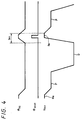
- FIG. 1 shows an embodiment of the present invention which is incorporated in a color CCD linear sensor.
- a color CCD linear sensor is generally designated by reference numeral 1.
- the color CCD linear sensor 1 is formed of a plurality of sensor lines, in this embodiment three sensor lines, which are comprised of a single linear sensor (an image element), namely, a R(red) linear sensor 2R, a G(green) linear sensor 2G and a B(blue) linear sensor 2B.
- the R linear sensor 2R, the G linear sensor 2G and the B linear sensor 2B have a R sensor array 3r, a G sensor array 3g and a B sensor array 3b respectively, each array including a plurality of sensor portions 3.
- charge transfer registers which are referred to as CCD registers
- 4r, 4g and 4b which are for example constructed as two-phase drive CCDs, via reading gate portions 5r, 5g and 5b respectively while on the other sides of the sensor arrays 3r, 3g and 3b there are provided shutter drain regions 7r, 7g and 7b via shutter gate portions 6r, 6g and 6b respectively.
- an output gate portion 11 and a floating diffusion region 12 which becomes a charge voltage converter unit are formed and further, a reset gate portion 13 and a reset drain 14 adjoining the floating diffusion region are formed.
- An output circuit 15 is connected to the floating diffusion region 12.
- a reading gate pulses ⁇ ROG is applied to the reading gate portions 5r, 5g and 5b, a reset pulse ⁇ RS is applied to the reset gate portion 13 and a fixed voltage is applied to the output gate portion 11.
- Two-phase drive clock pulses ⁇ 1 and ⁇ 2 are applied to the CCD registers 4r, 4g and 4b and particularly a drive clock pulse ⁇ LH which is the same to the ⁇ 1 , is applied to the end stage of the transfer portion.
- a shutter means is formed of each of the shutter gate portions 6r, 6g and 6b and the shutter drain regions 7r, 7g and 7b.
- shutter pulses ⁇ SHUT-R , ⁇ SHUT-G and ⁇ SHUT-B See FIG. 2 are applied to the shutter gate portions 6r, 6g and 6b respectively, the signal charges which have been accumulated in the sensor arrays 3r, 3g and 3b are discharged to the shutter drain regions 7r, 7g and 7b via the shutter gate portions 6r, 6g and 6b respectively.
- the period from the time when the reading gate pulse ⁇ ROG is applied to the time when the subsequent reading gate pulse ⁇ ROG is applied is ⁇ ROG and this ⁇ ROG is set as a period for accumulating the charge in the sensor portion 3 (which is defined as 1H period).
- This 1H period consists of an effective signal period T A for transferring and outputting the signal charge and the subsequent non-transfer period T B .
- the signal charges which have been accumulated in the respective sensor arrays 3r, 3g and 3b by means of photo-electric conversion are read simultaneously to the CCD registers 4r, 4g and 4b respectively by applying the reading gate pulse ⁇ ROG to the reading gate portions 5r, 5g and 5b.
- the two-phase drive clock pulses ⁇ 1 , ⁇ 2 and ⁇ LH are applied to the CCD registers 4r, 4g and 4b, the charges are transferred during the effective signal period T A of FIG. 2 and the signal charge at each one pixel (sensor portion) is read via the floating diffusion regions 12 as an output signal by the output circuit 15.
- the floating diffusion region 12 is reset when the reset pulse ⁇ RS is supplied to the reset gate portions 13 at each pixel.
- the non-transfer period T B from the end of the effective signal period T A and before the subsequent reading gate pulse ⁇ ROG is applied is a state such that no charge is transferred.
- the input of the shutter pulses ⁇ SHUT-R , ⁇ SHUT-G , and ⁇ SHUT-B can be performed.
- the shutter pulses ⁇ SHUT-R , ⁇ SHUT-G , and ⁇ SHUT-B are input in synchronism with the reset period T RS of the floating diffusion region 12 or the charge voltage converter portions. In this way, the shutter operation can be performed during the reset period T RS of the reset pulse ⁇ RS .
- the shutter pulse ⁇ SHUT is off.
- the shutter pulse ⁇ SHUT is applied during the period T RS when the reset pulse ⁇ RS is applied in the effective signal period T A .
- the shutter pulse ⁇ SHUT-R is not input to the R linear sensor 2R which has the lowest sensibility among the R linear sensor 2R, the G linear sensor 2G and the B linear sensor 2B, but the shutter pulses ⁇ SHUT-G and ⁇ SHUT-B are input to the G linear sensor 2G and the B linear sensor 2B respectively.
- the effective accumulating times of the R linear sensor 2R, the G linear sensor 2G and the B-linear sensor 2B become t R , t G and t B respectively.
- the input times of the shutter pulses ⁇ SHUT ( ⁇ SHUT-R , ⁇ SHUT-G and ⁇ SHUT-B ) can be set at any time in the 1H period whether in or out the effective signal period T A and therefore the variable ranges of the effective accumulating times t R , t G and t B of respective colors by the shutter control can be set wider than that of the prior art. Further, the influence of the coupling of the shutter pulses ⁇ SHUT on the wave form of output signal can be suppressed.
- the floating diffusion region is used as the charge voltage converter portion, but the floating gate or the like can be also used.
- the present invention is applied to the color CCD linear sensor 1 having three single linear sensors 2R, 2G and 2B but may be applied to a color CCD linear sensor having a plurality of, other than three, single linear sensors. Further, the present invention can be applied to a single color linear sensor.
- the present invention can also be applied to a CCD area sensor.
- the shutter operation is performed in synchronism with the reset period of the charge voltage converter portion which is connected to a horizontal transfer register.
- the influence of the coupling based on the shutter operation is not affected on the wave form of output signal and the shutter operation can be performed at anytime of the period including the period of reading a signal. Accordingly, the variable range of the effective accumulating period by the shutter control can be set wider than that of the related art.
Landscapes
- Engineering & Computer Science (AREA)
- Multimedia (AREA)
- Signal Processing (AREA)
- Physics & Mathematics (AREA)
- Spectroscopy & Molecular Physics (AREA)
- Electromagnetism (AREA)
- Transforming Light Signals Into Electric Signals (AREA)
- Solid State Image Pick-Up Elements (AREA)
Abstract
Description
Claims (19)
- A solid-state imaging device, comprising:a sensor portion for accumulating a signal charge produced by photoelectric conversion;a charge transfer register for transferring said signal charge;a charge/voltage converting portion connected to said charge transfer register; anda means for carrying out a shutter operation for discharging the charge accumulated by said sensor portion in synchronisation with a signal charge reset period of said charge/voltage converting portion.
- A solid-state imaging device according to claim 1, further comprising:a plurality of line sensors, wherein said means for carrying out the shutter operation discharges a charge accumulated by a line sensor having a higher sensitivity as compared with a line sensor having the lowest sensitivity among those of said plurality of line sensors.
- A solid-state imaging device according to claim 1, wherein a charge reset is carried out by applying a reset pulse to said charge/voltage converting portion during said signal charge reset period.
- A solid-state imaging device according to claim 3, wherein said means for carrying out the shutter operation applies a shutter pulse during a period when said reset pulse is applied to said charge/voltage converting portion.
- A solid-state imaging device according to claim 3, wherein said means for carrying out the shutter operation sets a shutter pulse in its off level during the period when said reset pulse is applied to said charge/voltage converting portion.
- A solid-state imaging device according to claim 1, wherein said charge/voltage converting portion comprises a floating diffusion portion.
- A solid-state imaging device according to claim 1, wherein said charge/voltage converting portion comprises a floating gate.
- A method of driving a solid-state imaging device having a sensor portion for accumulating a signal charge generated by photoelectric conversion, a charge transfer register, and a charge/voltage converting portion connected to said charge transfer register, comprising the step of:carrying out a shutter operation for discharging a charge accumulated by said sensor portion in synchronization with a reset period of said charge/voltage converting portion.
- A method of driving a solid-state imaging device according to claim 8, wherein said solid-state imaging device comprises a plurality of line sensors, and in said shutter operation a charge accumulated by a line sensor having a higher sensitivity as compared with a line sensor the lowest sensitivity among those of said plurality of line sensors.
- A method of driving a solid-state imaging device according to claim 8, wherein a charge reset is carried out by applying a reset pulse to said charge/voltage converting portion during said signal charge reset period.
- A method of driving a solid-state imaging device according to claim 8, wherein said means for carrying out the shutter operation applies a shutter pulse during a period when said reset pulse is applied to said charge/voltage converting portion.
- A method of driving a solid-state imaging device according to claim 10, wherein said means for carrying out the shutter operation sets a shutter pulse in its off level during the period when said reset pulse is applied to said charge/voltage converting portion.
- A method of driving a solid-state imaging device according to claim 8, wherein said charge/voltage converting portion comprises a floating diffusion portion.
- A method of driving a solid-state imaging device according to claim 8, wherein said charge/voltage converting portion comprises a floating gate.
- A method of driving a solid-state imaging device having a plurality of line sensors each of which has a sensor line with a plurality of sensor portions for accumulating charges generated by photoelectric conversion and a charge transfer register for transferring said signal charges and a charge/voltage converting portion connected to said plurality of charge transfer registers, comprising the step of:carrying out a shutter operation for discharging the charges accumulated by said sensor lines in synchronization with a reset period of said charge/voltage converting portion.
- A method of driving a solid-state imaging device according to claim 15, wherein said solid-state imaging device comprises a plurality of line sensors, and in said shutter operation a charge accumulated by a line sensor having a higher sensitivity as compared with a line sensor having the lowest sensitivity among those of said plurality of line sensors.
- A method of driving a solid-state imaging device according to claim 15, wherein a charge reset is carried out by applying a reset pulse to said charge/voltage converting portion during said signal charge reset period.
- A method of driving a solid-state imaging device according to claim 15, wherein said means for carrying out the shutter operation applies a shutter pulse during a period when said reset pulse is applied to said charge/voltage converting portion.
- A method of driving a solid-state imaging device according to claim 15, wherein said means for carrying out the shutter operation sets a shutter pulse in its off level during the period when said reset pulse is applied to said charge/voltage converting portion.
Applications Claiming Priority (3)
| Application Number | Priority Date | Filing Date | Title |
|---|---|---|---|
| JP329924/96 | 1996-12-10 | ||
| JP32992496 | 1996-12-10 | ||
| JP32992496A JP3637707B2 (en) | 1996-12-10 | 1996-12-10 | Solid-state imaging device and driving method thereof |
Publications (2)
| Publication Number | Publication Date |
|---|---|
| EP0848546A1 true EP0848546A1 (en) | 1998-06-17 |
| EP0848546B1 EP0848546B1 (en) | 2003-06-18 |
Family
ID=18226798
Family Applications (1)
| Application Number | Title | Priority Date | Filing Date |
|---|---|---|---|
| EP97121568A Expired - Lifetime EP0848546B1 (en) | 1996-12-10 | 1997-12-08 | Solid-state imaging device and method for driving the same |
Country Status (4)
| Country | Link |
|---|---|
| US (1) | US6473125B1 (en) |
| EP (1) | EP0848546B1 (en) |
| JP (1) | JP3637707B2 (en) |
| DE (1) | DE69722903T2 (en) |
Cited By (1)
| Publication number | Priority date | Publication date | Assignee | Title |
|---|---|---|---|---|
| US6728009B1 (en) | 1999-02-11 | 2004-04-27 | Fujifilm Electronic Imaging Limited | Charge coupled device scanning system and method |
Families Citing this family (9)
| Publication number | Priority date | Publication date | Assignee | Title |
|---|---|---|---|---|
| JP3141940B2 (en) * | 1998-05-08 | 2001-03-07 | 日本電気株式会社 | Color linear image sensor |
| JP4665276B2 (en) * | 1999-11-08 | 2011-04-06 | ソニー株式会社 | Solid-state imaging device and driving method thereof |
| TW510980B (en) * | 2000-12-12 | 2002-11-21 | Veutron Corp | Method for balancing different color channel outputs of color sensor |
| JP4024057B2 (en) * | 2002-03-06 | 2007-12-19 | 富士フイルム株式会社 | Digital camera |
| JP4587642B2 (en) * | 2003-01-21 | 2010-11-24 | ルネサスエレクトロニクス株式会社 | Linear image sensor |
| JP4082276B2 (en) * | 2003-05-26 | 2008-04-30 | セイコーエプソン株式会社 | Imaging apparatus and driving method thereof |
| JP3832661B2 (en) * | 2003-12-12 | 2006-10-11 | ソニー株式会社 | Driving method of solid-state imaging device |
| JP4758616B2 (en) * | 2004-04-13 | 2011-08-31 | ルネサスエレクトロニクス株式会社 | Linear image sensor |
| JP5103913B2 (en) * | 2007-01-30 | 2012-12-19 | ソニー株式会社 | Imaging device and video signal generator |
Citations (2)
| Publication number | Priority date | Publication date | Assignee | Title |
|---|---|---|---|---|
| WO1992006564A1 (en) * | 1990-09-28 | 1992-04-16 | Eastman Kodak Company | Image sensor |
| WO1993025042A1 (en) * | 1992-06-01 | 1993-12-09 | Eastman Kodak Company | Lateral overflow gate driver circuit for linear ccd sensor |
Family Cites Families (3)
| Publication number | Priority date | Publication date | Assignee | Title |
|---|---|---|---|---|
| US5606366A (en) * | 1991-10-28 | 1997-02-25 | Canon Kabushiki Kaisha | Image sensor driving apparatus wherein photoelectric conversion operations are performed a plurality of times |
| JPH04170175A (en) * | 1990-11-02 | 1992-06-17 | Canon Inc | Driver for solid-state image pickup element |
| JP3758205B2 (en) * | 1995-06-07 | 2006-03-22 | ソニー株式会社 | Solid-state imaging device, video camera using the same, and driving method of XY address type solid-state imaging device |
-
1996
- 1996-12-10 JP JP32992496A patent/JP3637707B2/en not_active Expired - Fee Related
-
1997
- 1997-12-08 DE DE69722903T patent/DE69722903T2/en not_active Expired - Lifetime
- 1997-12-08 EP EP97121568A patent/EP0848546B1/en not_active Expired - Lifetime
- 1997-12-09 US US08/987,387 patent/US6473125B1/en not_active Expired - Lifetime
Patent Citations (2)
| Publication number | Priority date | Publication date | Assignee | Title |
|---|---|---|---|---|
| WO1992006564A1 (en) * | 1990-09-28 | 1992-04-16 | Eastman Kodak Company | Image sensor |
| WO1993025042A1 (en) * | 1992-06-01 | 1993-12-09 | Eastman Kodak Company | Lateral overflow gate driver circuit for linear ccd sensor |
Non-Patent Citations (2)
| Title |
|---|
| SLESSOR M D ET AL: "A SIMPLE AND LOW-COST CCD-BASED IMAGING SYSTEM", MEASUREMENT SCIENCE AND TECHNOLOGY (FOR THE WHOLE COLLECTION USE BOCA..LI MAX), vol. 3, no. 4, 1 April 1992 (1992-04-01), pages 421 - 423, XP000290912 * |
| YOSHINORI KUNO ET AL: "A 7K-PIXELX3 LINE COLOR LINEAR SENSOR WITH SINGLE-SIDE READOUT METHOD", IEEE TRANSACTIONS ON CONSUMER ELECTRONICS, vol. 41, no. 3, 1 August 1995 (1995-08-01), pages 436 - 440, XP000539488 * |
Cited By (1)
| Publication number | Priority date | Publication date | Assignee | Title |
|---|---|---|---|---|
| US6728009B1 (en) | 1999-02-11 | 2004-04-27 | Fujifilm Electronic Imaging Limited | Charge coupled device scanning system and method |
Also Published As
| Publication number | Publication date |
|---|---|
| JPH10174001A (en) | 1998-06-26 |
| DE69722903D1 (en) | 2003-07-24 |
| DE69722903T2 (en) | 2004-05-19 |
| EP0848546B1 (en) | 2003-06-18 |
| US6473125B1 (en) | 2002-10-29 |
| JP3637707B2 (en) | 2005-04-13 |
Similar Documents
| Publication | Publication Date | Title |
|---|---|---|
| US5438364A (en) | Solid state color imager with on-chip color balance | |
| EP2378764B1 (en) | A camera | |
| US20060098109A1 (en) | Charge transfer device and a driving method thereof and a driving method for solid-state image sensing device | |
| JPH09162381A (en) | Linear sensor | |
| US5801850A (en) | Linear sensor having a plurality of sensor rows | |
| US4528595A (en) | Line transfer imager and television camera including such an imager | |
| US8120567B2 (en) | Shift register, and solid state image sensor and camera using shift register | |
| US6473125B1 (en) | Solid-state imaging device with shutter operation in sync with signal charge reset and method of driving same | |
| US6002497A (en) | Three-line linear sensor | |
| US5841554A (en) | Image pickup apparatus | |
| US4603343A (en) | Solid state image sensor applied with differing read-out gate voltages | |
| US20020006232A1 (en) | Analogue signal processing circuit | |
| US6980244B1 (en) | Solid state image pickup device, driving method thereof and camera | |
| US5973736A (en) | Color linear sensor | |
| JP3057534B2 (en) | Linear sensor and driving method thereof | |
| JP3155877B2 (en) | Solid-state imaging device and charge transfer method thereof | |
| JP3815495B2 (en) | Solid-state imaging device and driving method thereof | |
| JPH11164087A (en) | Solid-state imaging device and driving method therefor | |
| JPH09205520A (en) | Three-line linear sensor | |
| JP2763292B2 (en) | Image sensor | |
| JPH10327293A (en) | Picture reader | |
| JP2001157119A (en) | Method of driving solid-state image pickup device | |
| JPH11313256A (en) | Amplifier type solid-state image pickup device | |
| US20060087576A1 (en) | Charge transfer device, and control method therefor | |
| JP2994430B2 (en) | Image reading device |
Legal Events
| Date | Code | Title | Description |
|---|---|---|---|
| PUAI | Public reference made under article 153(3) epc to a published international application that has entered the european phase |
Free format text: ORIGINAL CODE: 0009012 |
|
| AK | Designated contracting states |
Kind code of ref document: A1 Designated state(s): DE FR GB |
|
| AX | Request for extension of the european patent |
Free format text: AL;LT;LV;MK;RO;SI |
|
| 17P | Request for examination filed |
Effective date: 19981118 |
|
| AKX | Designation fees paid |
Free format text: DE FR GB |
|
| RBV | Designated contracting states (corrected) |
Designated state(s): DE FR GB |
|
| 17Q | First examination report despatched |
Effective date: 20011130 |
|
| GRAH | Despatch of communication of intention to grant a patent |
Free format text: ORIGINAL CODE: EPIDOS IGRA |
|
| GRAH | Despatch of communication of intention to grant a patent |
Free format text: ORIGINAL CODE: EPIDOS IGRA |
|
| GRAA | (expected) grant |
Free format text: ORIGINAL CODE: 0009210 |
|
| AK | Designated contracting states |
Designated state(s): DE FR GB |
|
| REG | Reference to a national code |
Ref country code: GB Ref legal event code: FG4D |
|
| REF | Corresponds to: |
Ref document number: 69722903 Country of ref document: DE Date of ref document: 20030724 Kind code of ref document: P |
|
| PLBE | No opposition filed within time limit |
Free format text: ORIGINAL CODE: 0009261 |
|
| STAA | Information on the status of an ep patent application or granted ep patent |
Free format text: STATUS: NO OPPOSITION FILED WITHIN TIME LIMIT |
|
| ET | Fr: translation filed | ||
| 26N | No opposition filed |
Effective date: 20040319 |
|
| REG | Reference to a national code |
Ref country code: GB Ref legal event code: 746 Effective date: 20120703 |
|
| REG | Reference to a national code |
Ref country code: DE Ref legal event code: R084 Ref document number: 69722903 Country of ref document: DE Effective date: 20120614 |
|
| PGFP | Annual fee paid to national office [announced via postgrant information from national office to epo] |
Ref country code: GB Payment date: 20121220 Year of fee payment: 16 |
|
| PGFP | Annual fee paid to national office [announced via postgrant information from national office to epo] |
Ref country code: FR Payment date: 20130130 Year of fee payment: 16 |
|
| GBPC | Gb: european patent ceased through non-payment of renewal fee |
Effective date: 20131208 |
|
| REG | Reference to a national code |
Ref country code: FR Ref legal event code: ST Effective date: 20140829 |
|
| PG25 | Lapsed in a contracting state [announced via postgrant information from national office to epo] |
Ref country code: GB Free format text: LAPSE BECAUSE OF NON-PAYMENT OF DUE FEES Effective date: 20131208 Ref country code: FR Free format text: LAPSE BECAUSE OF NON-PAYMENT OF DUE FEES Effective date: 20131231 |
|
| PGFP | Annual fee paid to national office [announced via postgrant information from national office to epo] |
Ref country code: DE Payment date: 20141211 Year of fee payment: 18 |
|
| REG | Reference to a national code |
Ref country code: DE Ref legal event code: R119 Ref document number: 69722903 Country of ref document: DE |
|
| PG25 | Lapsed in a contracting state [announced via postgrant information from national office to epo] |
Ref country code: DE Free format text: LAPSE BECAUSE OF NON-PAYMENT OF DUE FEES Effective date: 20160701 |