EP0808057B1 - Verfahren und Vorrichtung zum Korrigieren eines Ausgangssignals eines Zeilensensors - Google Patents
Verfahren und Vorrichtung zum Korrigieren eines Ausgangssignals eines Zeilensensors Download PDFInfo
- Publication number
- EP0808057B1 EP0808057B1 EP97107819A EP97107819A EP0808057B1 EP 0808057 B1 EP0808057 B1 EP 0808057B1 EP 97107819 A EP97107819 A EP 97107819A EP 97107819 A EP97107819 A EP 97107819A EP 0808057 B1 EP0808057 B1 EP 0808057B1
- Authority
- EP
- European Patent Office
- Prior art keywords
- pixel
- corrected
- signal
- pixel signal
- level
- Prior art date
- Legal status (The legal status is an assumption and is not a legal conclusion. Google has not performed a legal analysis and makes no representation as to the accuracy of the status listed.)
- Expired - Lifetime
Links
- 238000000034 method Methods 0.000 title claims description 34
- 238000012545 processing Methods 0.000 claims description 13
- 238000012937 correction Methods 0.000 description 30
- 230000008569 process Effects 0.000 description 27
- 230000001419 dependent effect Effects 0.000 description 12
- 238000012546 transfer Methods 0.000 description 9
- 230000005484 gravity Effects 0.000 description 7
- 238000010586 diagram Methods 0.000 description 6
- 238000009792 diffusion process Methods 0.000 description 5
- 230000003287 optical effect Effects 0.000 description 4
- 230000004044 response Effects 0.000 description 4
- 230000015556 catabolic process Effects 0.000 description 3
- 230000008859 change Effects 0.000 description 3
- 238000006731 degradation reaction Methods 0.000 description 3
- 230000000694 effects Effects 0.000 description 3
- 238000003491 array Methods 0.000 description 2
- 230000000737 periodic effect Effects 0.000 description 2
- 230000016776 visual perception Effects 0.000 description 2
- 229910052782 aluminium Inorganic materials 0.000 description 1
- XAGFODPZIPBFFR-UHFFFAOYSA-N aluminium Chemical compound [Al] XAGFODPZIPBFFR-UHFFFAOYSA-N 0.000 description 1
- 230000008901 benefit Effects 0.000 description 1
- 238000001444 catalytic combustion detection Methods 0.000 description 1
- 230000006870 function Effects 0.000 description 1
- 238000009499 grossing Methods 0.000 description 1
- 229910052736 halogen Inorganic materials 0.000 description 1
- 150000002367 halogens Chemical class 0.000 description 1
- 230000007246 mechanism Effects 0.000 description 1
- 229910052751 metal Inorganic materials 0.000 description 1
- 239000002184 metal Substances 0.000 description 1
- 238000012986 modification Methods 0.000 description 1
- 230000004048 modification Effects 0.000 description 1
- 238000013441 quality evaluation Methods 0.000 description 1
- 238000005303 weighing Methods 0.000 description 1
Images


Classifications
-
- H—ELECTRICITY
- H04—ELECTRIC COMMUNICATION TECHNIQUE
- H04N—PICTORIAL COMMUNICATION, e.g. TELEVISION
- H04N1/00—Scanning, transmission or reproduction of documents or the like, e.g. facsimile transmission; Details thereof
- H04N1/40—Picture signal circuits
- H04N1/409—Edge or detail enhancement; Noise or error suppression
- H04N1/4092—Edge or detail enhancement
Definitions
- the present invention relates to an apparatus for and a method of correcting an output signal from a linear image sensor such as a CCD (charge-coupled device) in an image reading system.
- a linear image sensor such as a CCD (charge-coupled device) in an image reading system.
- Image reading systems operate by applying illuminating light to a subject placed on a subject table, guiding light representing image information carried by the subject as reflected or transmitted light to a focusing optical system, and photoelectrically reading the light with a linear image sensor such as a CCD or the like.
- the subject is read in a main scanning direction by the linear image sensor while at the same time the subject is moved relatively to the linear image sensor in an auxiliary scanning direction that is substantially perpendicular to the main scanning direction, so that two-dimensional image information can be produced.
- the light L which is detected by the photodetector 2 is converted into electric charges by the respective pixels P.
- the electric charges are successively shifted from the odd- and even-numbered pixels Po, Pe to the corresponding odd- and even-numbered pixel transfer arrays 3o, 3e in response to shift pulses that are periodically generated at constant time intervals. Thereafter, the electric charges are outputted as odd- and even-numbered pixel signals So, Se from odd- and even-numbered output sections 4o, 4e of FDAs (floating diffusion amplifiers) or the like through respective output terminals of the linear image sensor. 1.
- FDAs floating diffusion amplifiers
- the odd- and even-numbered pixel signals So, Se are alternately read through a variable-gain amplifier and a selector switch (not shown), and then converted by an A/D (analog-to-digital) converter (not shown) into a digital image signal, which is then stored in a line memory or the like.
- A/D analog-to-digital
- an actual halftone-dot image outputted on the basis of the image signal contains a beat pattern produced by the superimposition of the periodic stripes and properties due to screen angles and screen ruling.
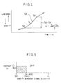
- FIG. 7 of the accompanying drawings shows such weighting coefficients k used in the proposed correction process.
- the weighting coefficients k are represented by the vertical axis, and the density D represented by the horizontal axis becomes progressively smaller toward a highlight (HL) area and larger toward a shadow (SD) area.
- the luminance of the original image, which is represented by the horizontal axis becomes progressively larger toward the highlight (HL) area and smaller toward the shadow (SD) area.
- the weighting coefficient k has a value of 1, and hence the corrected pixel signal Sc is determined according to the equation (1).
- the weighting coefficient k of the moving average is progressively larger from the density Db toward the density Da.
- the image data of a reproduced image at a positive-going edge thereof in the main scanning direction is smaller than the original image data which are not corrected due to a data-reducing image data shift by half pixel in the main scanning direction, and the image data of a reproduced image at a negative-going edge thereof in the main scanning direction is larger than the original image data which is not corrected due to a data-increasing image data shift by half pixel in the main scanning direction.
- US-A-5 408 338 discloses an image processing system in which the intensity of each pixel can be corrected to be an average intensity of a predetermined number of pixels surrounding each pixel in a predetermined area.
- the intensity of the pixel is corrected in accordance with the direction in which the edge faces.
- the focusing unit 18 comprises a plurality of prisms 32a ⁇ 32c mounted on a lower surface of a base 28 having a slit 31 defined therein.
- the prisms 32a ⁇ 32c serve to separate the transmitted light into lights R, G, B.
- Linear image sensors 1a ⁇ 1c in the form of CCDs are fixed as photoelectric transducers to the respective prisms 32a ⁇ 32c.
- Each of the linear image sensors 1a ⁇ 1c is basically of the same structure as the linear image sensor shown in FIG. 6.
- the image signals Sd are supplied from the A/D converter 55 through an input port 60.
- the image signals are stored in FIFO shift registers (storage means referred to as registers) 61, 62, 63 serving as memory means under the control of a CPU (control means). If the register 62 stores the level S of a pixel signal S, then the register 63 stores the level Sp of a pixel signal (preceding pixel signal) Sp which precedes the pixel signal S, and the register 61 stores the level Sa of a pixel signal (following pixel signal) Sa which follows the pixel signal S.
- FIFO shift registers storage means referred to as registers
- the register 63 stores the level Sp of a pixel signal (preceding pixel signal) Sp which precedes the pixel signal S
- the register 61 stores the level Sa of a pixel signal (following pixel signal) Sa which follows the pixel signal S.
- the pixel signals stored in the registers 61, 63 on the opposite sides of the central register 62 are even-numbered pixel signals Se (though they are denoted by "Se” used for analog pixel signals in FIG. 2, they are actually digital signals when stored in the registers).
- the pixel signal S stored in the central register 62 is an even-numbered pixel signal Se
- the pixel signals stored in the registers 61, 63 are odd-numbered pixel signals So.
- the pixel signal S or a corrected pixel signal S' which is the calculated pixel signal Sc is outputted from the selector switch 72 to an output terminal 74 for further processing.
- the signal correcting circuit 56 outputs the moving average signal Sc relative to the three successive pixel signals as the corrected image signal S'.
- final values of the reference density level Dr and the contrast density level Cr should preferably be determined through image quality evaluations in view of the overall characteristics of the image reading and platemaking system.
Landscapes
- Engineering & Computer Science (AREA)
- Multimedia (AREA)
- Signal Processing (AREA)
- Facsimile Image Signal Circuits (AREA)
- Transforming Light Signals Into Electric Signals (AREA)
- Facsimile Scanning Arrangements (AREA)
- Image Input (AREA)
Claims (4)
- Vorrichtung zum Korrigieren jedes einer ungeraden Anzahl von Pixelsignalen (So) und einer geraden Anzahl von Pixelsignalen (Se), die von einem linearen Bildsensor (1) ausgegeben und abwechselnd gelesen werden, um ein Bildsignal (Sd) zu bilden, umfassend:eine Speichereinrichtung (61-63) zum Speichern eines Pegels (S) eines zu korrigierenden Pixelsignals und von Pegeln (Sp, Sa) eines vorausgehenden und eines nachfolgenden Pixelsignals, die dem zu korrigierenden Pixelsignal vorausgehen bzw. nachfolgen; undeine Berechnungseinrichtung (71), die an eine Speichereinrichtung (61-63) angeschlossen ist, um den Pegel (S) des zu korrigierenden Pixelsignals und die Pegel (Sp, Sa) des vorausgehenden und nachfolgenden Pixelsignals zu verarbeiten und ein korrigierendes Pixelsignal (Sc) zu erzeugen, wobei die Berechnungseinrichtung (71) eine Einrichtung aufweist, um den Pegel (Sc) des korrigierten Signals gemäß folgender Gleichung zu bestimmen:wobei S den Pegel des zu korrigierenden Pixelsignals, Sp den Pegel des vorhergehenden Pixelsignals und Sa den Pegel des nachfolgenden Pixelsignals bedeutet,

gekennzeichnet durch eine Auswahleinrichtung (72, 73, 75, 76, 77, 78) zum Auswählen und Ausgeben des zu korrigierenden Pixelsignals oder des korrigierten Pixelsignals (Sc) basierend auf einem Durchschnitt (Dx) der oder einer Differenz (Cx) zwischen den Pegeln (Sp, Sa) des vorausgehenden und des nachfolgenden Pixelsignals, wobei die Auswahleinrichtung eine Einrichtung aufweist zum Auswählen und Ausgeben des korrigierten Pixelsignals (Sc), wenn der Durchschnittswert {(Sp + Sa)/2} der Pegel (Sp, Sa) des vorhergehenden und des folgenden Pixelsignals kleiner ist als ein erster Referenzwert, und der Absolutwert der Differenz (Sp-Sa) zwischen den Pegeln (Sp, Sa) des vorhergehenden und des nachfolgenden Pixelsignals kleiner als ein zweiter Referenzwert ist, und zum Auswählen und Ausgeben des zu korrigierenden Pixelsignals sonst. - Vorrichtung nach Anspruch 1, bei der der lineare Bildsensor ein linearer CCD-Bildsensor ist.
- Verfahren zum Korrigieren jedes aus einer ungeraden Anzahl von Pixelsignalen (So) und einer geraden Anzahl von Pixelsignalen (Se), die von einem linearen Bildsensor (1) ausgegeben und abwechselnd gelesen werden, um ein Bildsignal (Sd) zu erzeugen, umfassend folgende Schritte:
Verarbeiten eines zu korrigierenden Pixelsignals (S) und eines vorausgehenden und nachfolgenden Pixelsignals (Sp, Sa), die dem zu korrigierenden Pixelsignal vorausgehen bzw. nachfolgen, um ein korrigiertes Pixelsignal (Sc) zu erzeugen, wobei der Verarbeitungsschritt den Schritt beinhaltet, bei dem ein erster Durchschnittswert ((Sp + 2S + Sa)/4) des zu korrigierenden Pixelsignals (S) und ein zweiter Durchschnittswert ((Sp + Sa)/2) des vorhergehenden und des nachfolgenden Pixelsignals berechnet werden, dadurch gekennzeichnet, dass der erste Durchschnittswert ((Sp + 2S + Sa)/4) als das korrigierte Pixelsignal (Sc) ausgegeben wird, wenn die Dichte des zweiten Durchschnittswerts ((Sp + Sa)/2) des vorhergehenden und des nachfolgenden Pixelsignals (Sp, Sa) größer ist als ein vorbestimmter Dichtewert, und der Kontrast (Sa-Sp), der auf der Grundlage des Absolutwerts der Differenz zwischen den Pegeln (Sp, Sa) des vorhergehenden und des nachfolgenden Pixelsignals berechnet wird, kleiner als ein vorbestimmter Kontrastwert ist, ansonsten das zu korrigierende Pixelsignal (S) als das korrigierte Pixelsignal ausgegeben wird. - Verfahren nach Anspruch 3, bei dem der lineare Bildsensor einen linearen CCD-Bildsensor aufweist.
Applications Claiming Priority (2)
| Application Number | Priority Date | Filing Date | Title |
|---|---|---|---|
| JP12373496A JP3738080B2 (ja) | 1996-05-17 | 1996-05-17 | リニアイメージセンサの出力信号補正装置 |
| JP123734/96 | 1996-05-17 |
Publications (3)
| Publication Number | Publication Date |
|---|---|
| EP0808057A2 EP0808057A2 (de) | 1997-11-19 |
| EP0808057A3 EP0808057A3 (de) | 1999-01-07 |
| EP0808057B1 true EP0808057B1 (de) | 2006-12-13 |
Family
ID=14868028
Family Applications (1)
| Application Number | Title | Priority Date | Filing Date |
|---|---|---|---|
| EP97107819A Expired - Lifetime EP0808057B1 (de) | 1996-05-17 | 1997-05-13 | Verfahren und Vorrichtung zum Korrigieren eines Ausgangssignals eines Zeilensensors |
Country Status (4)
| Country | Link |
|---|---|
| EP (1) | EP0808057B1 (de) |
| JP (1) | JP3738080B2 (de) |
| CN (1) | CN1116761C (de) |
| DE (1) | DE69737079T2 (de) |
Families Citing this family (6)
| Publication number | Priority date | Publication date | Assignee | Title |
|---|---|---|---|---|
| JP2000307859A (ja) * | 1999-02-15 | 2000-11-02 | Seiko Epson Corp | 画像読取装置 |
| US7324236B2 (en) | 2000-02-01 | 2008-01-29 | Canon Kabushiki Kaisha | Discrepancy correction method and apparatus for correcting difference in levels of image signals obtained by an image sensor having a multiple output channels |
| JP4062175B2 (ja) * | 2003-01-09 | 2008-03-19 | セイコーエプソン株式会社 | 画像処理装置、方法、プログラムおよび該プログラムを記録した記録媒体 |
| JP2005348351A (ja) * | 2004-06-07 | 2005-12-15 | Ricoh Co Ltd | 画像読取装置及び画像形成装置 |
| JP2012085324A (ja) * | 2011-11-27 | 2012-04-26 | Yamaguchi Cinema Corp | 電荷増倍素子を用いた高感度・高速度の競技用電子判定装置 |
| JP2021068971A (ja) * | 2019-10-21 | 2021-04-30 | 京セラドキュメントソリューションズ株式会社 | 画像読取装置 |
Family Cites Families (9)
| Publication number | Priority date | Publication date | Assignee | Title |
|---|---|---|---|---|
| US3775559A (en) * | 1970-11-12 | 1973-11-27 | Xerox Corp | Aperture designs for facsimile scanning apparatus |
| JPS568140A (en) * | 1979-07-02 | 1981-01-27 | Dainippon Screen Mfg Co Ltd | Emphasizing method of sharpness in image scanning and recording apparatus |
| US4860118A (en) * | 1987-02-25 | 1989-08-22 | Canon Kabushiki Kaisha | Image signal processing apparatus with edge emphasis and variable magnification |
| US5319451A (en) * | 1988-05-31 | 1994-06-07 | Canon Kabushiki Kaisha | Color signal processing apparatus using a common low pass filter for the luminance signal and the color signals |
| EP0424111B1 (de) * | 1989-10-18 | 1997-06-18 | Sony Corporation | Vorrichtung zur Verarbeitung eines Videosignals |
| JPH04293359A (ja) * | 1991-03-22 | 1992-10-16 | Dainippon Screen Mfg Co Ltd | 画像読取装置 |
| JP3222183B2 (ja) * | 1992-02-19 | 2001-10-22 | 株式会社リコー | 画像処理装置 |
| JPH05284352A (ja) * | 1992-03-30 | 1993-10-29 | Asahi Glass Co Ltd | Ccdラインセンサ用ディジタルフィルタ |
| KR960003298A (ko) * | 1994-06-02 | 1996-01-26 | 이헌조 | 캠코더의 촬상관 결점보상 방법 및 장치 |
-
1996
- 1996-05-17 JP JP12373496A patent/JP3738080B2/ja not_active Expired - Fee Related
-
1997
- 1997-05-13 DE DE69737079T patent/DE69737079T2/de not_active Expired - Lifetime
- 1997-05-13 EP EP97107819A patent/EP0808057B1/de not_active Expired - Lifetime
- 1997-05-17 CN CN97112981A patent/CN1116761C/zh not_active Expired - Fee Related
Also Published As
| Publication number | Publication date |
|---|---|
| CN1170298A (zh) | 1998-01-14 |
| JP3738080B2 (ja) | 2006-01-25 |
| CN1116761C (zh) | 2003-07-30 |
| JPH09307764A (ja) | 1997-11-28 |
| EP0808057A2 (de) | 1997-11-19 |
| DE69737079D1 (de) | 2007-01-25 |
| DE69737079T2 (de) | 2007-07-12 |
| EP0808057A3 (de) | 1999-01-07 |
Similar Documents
| Publication | Publication Date | Title |
|---|---|---|
| JP3809226B2 (ja) | リニアイメージセンサの出力画像信号の補正方法 | |
| US4920428A (en) | Offset, gain and bad pixel correction in electronic scanning arrays | |
| JP3733446B2 (ja) | デジタル複写機 | |
| US4734762A (en) | Color image reading apparatus with a plurality of line sensors in which a white balance operation is performed by determining amplifier gains while reading a white reference plate | |
| US5483359A (en) | Color image scanning apparatus for reading a color original without color shift regardless of a magnification ratio of the original | |
| US5535007A (en) | Method and device for adjusting magnification of image | |
| JPH077617A (ja) | 色値処理方法および処理装置 | |
| JPS61227481A (ja) | 画像入力装置における補正用基準デ−タ取込方法 | |
| JPH04363967A (ja) | 原稿読取り装置 | |
| US5940125A (en) | Correcting offset level using a proportional distribution of a difference in dark current levels in a line image sensor | |
| EP0808057B1 (de) | Verfahren und Vorrichtung zum Korrigieren eines Ausgangssignals eines Zeilensensors | |
| EP1058448A2 (de) | Bildverarbeitungsgerät | |
| JPH0354679A (ja) | 画像処理装置 | |
| EP0420152B1 (de) | Verfahren und Vorrichtung zur Beseitigung von Falschbildern | |
| EP0424967B1 (de) | Bildsignalverarbeitungsanordnung | |
| EP1079602B1 (de) | Bildeingabevorrichtung | |
| JPH042262A (ja) | 画像読取装置 | |
| JP2592147B2 (ja) | 画像信号処理装置 | |
| JP3276026B2 (ja) | 画像読み取り装置の画像データ調整方法 | |
| JPS616978A (ja) | デジタル画像処理装置 | |
| JP2592146B2 (ja) | 画像信号処理装置 | |
| JPH02272878A (ja) | 原稿読取装置 | |
| JP3751422B2 (ja) | 画像読取装置 | |
| JP2003274122A (ja) | オリジナルイメージから電気的イメージ信号を生成する装置 | |
| JPH02211771A (ja) | 画像信号処理方法 |
Legal Events
| Date | Code | Title | Description |
|---|---|---|---|
| PUAI | Public reference made under article 153(3) epc to a published international application that has entered the european phase |
Free format text: ORIGINAL CODE: 0009012 |
|
| AK | Designated contracting states |
Kind code of ref document: A2 Designated state(s): DE FR GB |
|
| PUAL | Search report despatched |
Free format text: ORIGINAL CODE: 0009013 |
|
| AK | Designated contracting states |
Kind code of ref document: A3 Designated state(s): DE FR GB |
|
| 17P | Request for examination filed |
Effective date: 19990324 |
|
| 17Q | First examination report despatched |
Effective date: 20050315 |
|
| GRAP | Despatch of communication of intention to grant a patent |
Free format text: ORIGINAL CODE: EPIDOSNIGR1 |
|
| GRAS | Grant fee paid |
Free format text: ORIGINAL CODE: EPIDOSNIGR3 |
|
| RIN1 | Information on inventor provided before grant (corrected) |
Inventor name: SUGANUMA, ATSUSHI |
|
| GRAA | (expected) grant |
Free format text: ORIGINAL CODE: 0009210 |
|
| AK | Designated contracting states |
Kind code of ref document: B1 Designated state(s): DE FR GB |
|
| REG | Reference to a national code |
Ref country code: GB Ref legal event code: FG4D |
|
| REF | Corresponds to: |
Ref document number: 69737079 Country of ref document: DE Date of ref document: 20070125 Kind code of ref document: P |
|
| REG | Reference to a national code |
Ref country code: GB Ref legal event code: 732E |
|
| RAP2 | Party data changed (patent owner data changed or rights of a patent transferred) |
Owner name: FUJIFILM CORPORATION |
|
| ET | Fr: translation filed | ||
| REG | Reference to a national code |
Ref country code: FR Ref legal event code: TP Ref country code: FR Ref legal event code: CD |
|
| PLBE | No opposition filed within time limit |
Free format text: ORIGINAL CODE: 0009261 |
|
| STAA | Information on the status of an ep patent application or granted ep patent |
Free format text: STATUS: NO OPPOSITION FILED WITHIN TIME LIMIT |
|
| 26N | No opposition filed |
Effective date: 20070914 |
|
| PGFP | Annual fee paid to national office [announced via postgrant information from national office to epo] |
Ref country code: GB Payment date: 20100329 Year of fee payment: 14 |
|
| PGFP | Annual fee paid to national office [announced via postgrant information from national office to epo] |
Ref country code: FR Payment date: 20100525 Year of fee payment: 14 |
|
| PGFP | Annual fee paid to national office [announced via postgrant information from national office to epo] |
Ref country code: DE Payment date: 20100415 Year of fee payment: 14 |
|
| REG | Reference to a national code |
Ref country code: DE Ref legal event code: R119 Ref document number: 69737079 Country of ref document: DE |
|
| REG | Reference to a national code |
Ref country code: DE Ref legal event code: R119 Ref document number: 69737079 Country of ref document: DE |
|
| GBPC | Gb: european patent ceased through non-payment of renewal fee |
Effective date: 20110513 |
|
| REG | Reference to a national code |
Ref country code: FR Ref legal event code: ST Effective date: 20120131 |
|
| PG25 | Lapsed in a contracting state [announced via postgrant information from national office to epo] |
Ref country code: FR Free format text: LAPSE BECAUSE OF NON-PAYMENT OF DUE FEES Effective date: 20110531 |
|
| PG25 | Lapsed in a contracting state [announced via postgrant information from national office to epo] |
Ref country code: GB Free format text: LAPSE BECAUSE OF NON-PAYMENT OF DUE FEES Effective date: 20110513 |
|
| PG25 | Lapsed in a contracting state [announced via postgrant information from national office to epo] |
Ref country code: DE Free format text: LAPSE BECAUSE OF NON-PAYMENT OF DUE FEES Effective date: 20111130 |