EP0808057A2 - Verfahren und Vorrichtung zum Korrigieren eines Ausgangssignals eines Zeilensensors - Google Patents
Verfahren und Vorrichtung zum Korrigieren eines Ausgangssignals eines Zeilensensors Download PDFInfo
- Publication number
- EP0808057A2 EP0808057A2 EP97107819A EP97107819A EP0808057A2 EP 0808057 A2 EP0808057 A2 EP 0808057A2 EP 97107819 A EP97107819 A EP 97107819A EP 97107819 A EP97107819 A EP 97107819A EP 0808057 A2 EP0808057 A2 EP 0808057A2
- Authority
- EP
- European Patent Office
- Prior art keywords
- corrected
- pixel
- pixel signal
- signal
- level
- Prior art date
- Legal status (The legal status is an assumption and is not a legal conclusion. Google has not performed a legal analysis and makes no representation as to the accuracy of the status listed.)
- Granted
Links
- 238000000034 method Methods 0.000 title claims abstract description 38
- 238000012545 processing Methods 0.000 claims description 9
- 238000012937 correction Methods 0.000 abstract description 33
- 230000008569 process Effects 0.000 abstract description 30
- 230000005484 gravity Effects 0.000 abstract description 8
- 230000001419 dependent effect Effects 0.000 description 12
- 238000012546 transfer Methods 0.000 description 9
- 238000010586 diagram Methods 0.000 description 6
- 238000009792 diffusion process Methods 0.000 description 5
- 230000003287 optical effect Effects 0.000 description 4
- 230000004044 response Effects 0.000 description 4
- 230000015556 catabolic process Effects 0.000 description 3
- 230000008859 change Effects 0.000 description 3
- 238000006731 degradation reaction Methods 0.000 description 3
- 230000000694 effects Effects 0.000 description 3
- 238000003491 array Methods 0.000 description 2
- 230000000737 periodic effect Effects 0.000 description 2
- 230000016776 visual perception Effects 0.000 description 2
- 229910052782 aluminium Inorganic materials 0.000 description 1
- XAGFODPZIPBFFR-UHFFFAOYSA-N aluminium Chemical compound [Al] XAGFODPZIPBFFR-UHFFFAOYSA-N 0.000 description 1
- 238000001444 catalytic combustion detection Methods 0.000 description 1
- 230000006870 function Effects 0.000 description 1
- 229910052736 halogen Inorganic materials 0.000 description 1
- 150000002367 halogens Chemical class 0.000 description 1
- 230000007246 mechanism Effects 0.000 description 1
- 229910052751 metal Inorganic materials 0.000 description 1
- 239000002184 metal Substances 0.000 description 1
- 238000012986 modification Methods 0.000 description 1
- 230000004048 modification Effects 0.000 description 1
- 238000013441 quality evaluation Methods 0.000 description 1
- 238000005303 weighing Methods 0.000 description 1
Images


Classifications
-
- H—ELECTRICITY
- H04—ELECTRIC COMMUNICATION TECHNIQUE
- H04N—PICTORIAL COMMUNICATION, e.g. TELEVISION
- H04N1/00—Scanning, transmission or reproduction of documents or the like, e.g. facsimile transmission; Details thereof
- H04N1/40—Picture signal circuits
- H04N1/409—Edge or detail enhancement; Noise or error suppression
- H04N1/4092—Edge or detail enhancement
Definitions
- the present invention relates to an apparatus for and a method of correcting an output signal from a linear image sensor such as a CCD (charge-coupled device) in an image reading system.
- a linear image sensor such as a CCD (charge-coupled device) in an image reading system.
- Image reading systems operate by applying illuminating light to a subject placed on a subject table, guiding light representing image information carried by the subject as reflected or transmitted light to a focusing optical system, and photoelectrically reading the light with a linear image sensor such as a CCD or the like.
- the subject is read in a main scanning direction by the linear image sensor while at the same time the subject is moved relatively to the linear image sensor in an auxiliary scanning direction that is substantially perpendicular to the main scanning direction, so that two-dimensional image information can be produced.
- a general linear image sensor 1 basically comprises a photodetector 2 comprising a linear array of photoelectric transducer elements (hereinafter referred to as "pixels") P and a pixel transfer unit 3 comprising an odd-numbered pixel transfer array 3o and an even-numbered pixel transfer array 3e which are positioned one on each side of the photodetector 2.
- the pixels P include odd-numbered pixels Po and even-numbered pixels Pe.
- the pixel transfer unit 3 is covered with a metal film (not shown) such as an evaporated aluminum film or the like which shields the pixel transfer unit 3 from light L.
- the light L which is detected by the photodetector 2 is converted into electric charges by the respective pixels P.
- the electric charges are successively shifted from the odd-and even-numbered pixels Po, Pe to the corresponding odd-and even-numbered pixel transfer arrays 3o, 3e in response to shift pulses that are periodically generated at constant time intervals. Thereafter, the electric charges are outputted as odd- and even-numbered pixel signals So, Se from odd- and even-numbered output sections 4o, 4e of FDAs (floating diffusion amplifiers) or the like through respective output terminals of the linear image sensor 1.
- FDAs floating diffusion amplifiers
- the odd- and even-numbered pixel signals So, Se are alternately read through a variable-gain amplifier and a selector switch (not shown), and then converted by an A/D (analog-to-digital) converter (not shown) into a digital image signal, which is then stored in a line memory or the like.
- A/D analog-to-digital
- the digital image signal stored in the line memory has different levels respectively for the odd- and even-numbered pixel signals So, Se because of linearity differences of the odd- and even-numbered pixel signals So, Se, i.e., different changes in the amplitudes of the electric charges with respect to a small change in the light intensity.
- the odd- and even-numbered pixel signals So, Se are observed for their waveforms, then their levels suffer rectangular wave ripples.
- an image is reproduced on the basis of the image signal, therefore, it contains periodic longitudinal stripes along the auxiliary scanning direction.
- an actual halftone-dot image outputted on the basis of the image signal contains a beat pattern produced by the superimposition of the periodic stripes and properties due to screen angles and screen ruling.
- the odd- and even-numbered pixel level difference correction process based on the equation (1) is disadvantageous in that if an original image contains thin longitudinal stripes along the auxiliary scanning direction, then a reproduced image based on pixel signals corrected by the odd- and even-numbered pixel level difference correction process tends to be blurred due to a degradation of MTF (modulation transfer function).
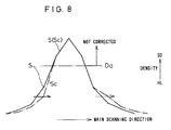
- human visual perception has a low MTF with respect to a low-density area of a reproduced image (a highlight area of an original image) and a high MTF with respect to a high-density area of the reproduced image (a shadow area of the original image), and proposed a correction process for correcting pixel signals with moving averages of a constant weighting coefficient in a high-density area where the density is higher than a value of 2.0 and correcting pixel signals with moving averages of progressively smaller weighting coefficients in a low-density area where the density is lower than the value of 2.0.
- FIG. 7 of the accompanying drawings shows such weighting coefficients k used in the proposed correction process.
- the weighting coefficients k are represented by the vertical axis, and the density D represented by the horizontal axis becomes progressively smaller toward a highlight (HL) area and larger toward a shadow (SD) area.
- the luminance of the original image, which is represented by the horizontal axis becomes progressively larger toward the highlight (HL) area and smaller toward the shadow (SD) area.
- the weighting coefficient k has a value of 1, and hence the corrected pixel signal Sc is determined according to the equation (1).
- the weighting coefficient k of the moving average is progressively larger from the density Db toward the density Da.
- Se outputted from the linear image sensor 1 are corrected by moving averages of two successive pixel signals depending on the density D, any MTF degradations in an image which contains thin longitudinal stripes along the auxiliary scanning direction are minimized to a level which cannot visually be perceived.
- the image data of a reproduced image at a positive-going edge thereof in the main scanning direction is smaller than the original image data which are not corrected due to a data-reducing image data shift by half pixel in the main scanning direction, and the image data of a reproduced image at a negative-going edge thereof in the main scanning direction is larger than the original image data which is not corrected due to a data-increasing image data shift by half pixel in the main scanning direction.
- Another object of the present invention is to provide an apparatus for and a method of correcting an output signal from a linear image sensor in a manner to prevent the center of gravity of a reproduced image from being positionally shifted after the output signal has been processed by an odd- and even-numbered pixel level difference correction process, and to effect the odd- and even-numbered pixel level difference correction process depending on the contents of an original image.
- FIGS. 1 through 5 Those parts of FIGS. 1 through 5 which are identical to those shown in FIGS. 6 through 8 are denoted by identical reference numerals and representations, and will not be described in detail below.
- FIGS. 6 through 8 will also be referred to when necessary in the description of the present invention.
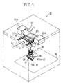
- FIG. 1 schematically shows an image reading system 10 to which the present invention is applied.
- the image reading system 10 has a feed mechanism 11 which moves a subject cassette 12 in the direction indicated by the arrow Y (auxiliary scanning direction Y) and an illuminating optical system (illuminating light source) 14 which applies illuminating light to the subject cassette 12 in the direction indicated by the arrow X (main scanning direction X or line direction X).
- Image information recorded on a transmissive subject F which is carried by the subject cassette 12 is carried by transmitted light L, which is focused by a focusing optical system 16 comprising a plurality of converging lenses onto a focusing unit 18.
- the focusing unit 18 converts the focused light L to an electric signal.
- the illuminating optical system 14 comprises a cylindrical diffusion chamber 22 having an inner light diffusion surface and a longitudinal slit 20, and a pair of light sources 24a, 24b mounted on the respective opposite ends of the cylindrical diffusion chamber 22 and each comprising a halogen lamp or the like.
- the focusing unit 18 comprises a plurality of prisms 32a ⁇ 32c mounted on a lower surface of a base 28 having a slit 31 defined therein.
- the prisms 32a ⁇ 32c serve to separate the transmitted light into lights R, G, B.
- Linear image sensors 1a ⁇ 1c in the form of CCDs are fixed as photoelectric transducers to the respective prisms 32a ⁇ 32c.
- Each of the linear image sensors 1a ⁇ 1c is basically of the same structure as the linear image sensor shown in FIG. 6.
- Odd- and even-numbered pixel signals So, Se outputted from the linear image sensors 1a ⁇ 1c are supplied through a flexible printed circuit to a signal processing board 34.
- the linear image sensors 1a ⁇ 1c effect an identical process of odd- and even-numbered pixel level difference correction as described below.
- the linear image sensors 1a ⁇ 1c will therefore be referred to collectively as a linear image sensor 1 unless they should separately be described.
- FIG. 2 schematically shows the linear image sensor 1 of the focusing unit 18 and a signal correcting apparatus according to the present invention for correcting level differences between the odd- and even-numbered pixel signals So, Se that are outputted from the linear image sensor 1.
- the transmitted light which carries the image information detected by the photodetector 2 is converted by the photoelectric transducer pixels P into electric charges, which are successively shifted from the odd- and even-numbered pixels P (P1, P2, P3, P4, ⁇ ) to the corresponding odd- and even-numbered pixel transfer arrays 3o, 3e in response to shift pulses that are periodically outputted from a timing generator (timing controller) 51. Thereafter, the electric charges are outputted as odd- and even-numbered pixel signals So, Se from odd- and even-numbered output sections 4o, 4e of FDAs (floating diffusion amplifiers) or the like through respective output terminals of the linear image sensor 1 in response to transfer clock pulses from the timing generator 51.
- FDAs floating diffusion amplifiers
- the odd- and even-numbered pixel signals So, Se are supplied through variable-gain amplifiers 52, 53 and a selector switch (multiplexer) 54, which are on the signal processing board 34, alternately in the sequence of pixels (P1, P2, ⁇ ) to an A/D (analog-to-digital) converter 55 having a 14-bit resolution.
- the A/D converter 55 converts the odd- and even-numbered pixel signals So, Se, which are analog signals, to digital image signals Sd that are supplied to a signal correcting circuit 56 which serves as an odd- and even-numbered pixel level difference correction circuit.
- A/D converters 55 may be connected parallel to each other to the output terminals of the respective variable-gain amplifiers 52, 53, and output digital signals from the A/D converters 55 may be switched by the multiplexer 54.
- FIG. 3 shows the signal correcting circuit 56 as an odd- and even-numbered pixel level difference correction circuit in greater detail.
- the image signals Sd are supplied from the A/D converter 55 through an input port 60.
- the image signals are stored in FIFO shift registers (storage means referred to as registers) 61, 62, 63 serving as memory means under the control of a CPU (control means). If the register 62 stores the level S of a pixel signal S, then the register 63 stores the level Sp of a pixel signal (preceding pixel signal) Sp which precedes the pixel signal S, and the register 61 stores the level Sp of a pixel signal (following pixel signal) Sa which follows the pixel signal S.
- FIFO shift registers storage means referred to as registers
- the register 63 stores the level Sp of a pixel signal (preceding pixel signal) Sp which precedes the pixel signal S
- the register 61 stores the level Sp of a pixel signal (following pixel signal) Sa which follows the pixel signal S.
- the level Sp of the pixel signal Sd of a certain pixel Pp (see FIG. 2) is stored in the register 61. Then, in synchronism with a next pixel clock pulse, the level Sp stored in the register 61 is shifted to the register 62, and the level S of the pixel signal Sd of a next pixel P is stored in the register 61. In synchronism with a next pixel clock pulse, the levels Sp, S are shifted from the registers 62, 61 respectively to the registers 63, 62, and the level Sa of the pixel signal of a next pixel Pa is stored in the register 61. Subsequently, each time a new pixel block pulse is applied, the pixel signals stored in the registers 61, 62, 63 are updated in the manner described above.
- the pixel signals stored in the registers 61, 63 on the opposite sides of the central register 62 are even-numbered pixel signals Se (though they are denoted by "Se” used for analog pixel signals in FIG. 2, they are actually digital signals when stored in the registers).
- the pixel signal S stored in the central register 62 is an even-numbered pixel signal Se
- the pixel signals stored in the registers 61, 63 are odd-numbered pixel signals So.
- the three successive pixel signals Sp, S, Sa are supplied to a successive three pixel weighted moving average calculating unit (calculating means) 71.
- the successive three pixel moving average calculating unit 71 calculates a weighted moving average of three successive pixels according to the equation (3), given below, and outputs a level Sc of a calculated pixel signal Sc.
- the pixel signal S is supplied from the register 62 to a terminal 72b of a selector switch or multiplexer (selecting means) 72, and the calculated pixel signal (corrected pixel signal) Sc is supplied from the successive three pixel weighted moving average calculating unit 71 to another terminal Sc of the selector switch 72.
- the selector switch 72 has a control signal 72d supplied with a selection control signal SE from a three-input AND gate (logic means) 73 which is part of the selecting means.
- the selector switch 72 also has a common terminal 72a which is selectively connected to the terminal 72c when the selection signal SE is of a high level and to the terminal 72b when the selection signal SE is of a low level.
- the pixel signal S or a corrected pixel signal S' which is the calculated pixel signal Sc is outputted from the selector switch 72 to an output terminal 74 for further processing.
- the preceding and following pixel signals Sp, Sa are supplied from the registers 63, 61 to a density calculating unit 75 and a contrast calculating unit 76.
- the density calculating unit 75 calculates a density dependent signal Dx (which is the same as the average U) according to the equation (4), given below, and supplies the density dependent signal Dx to a comparator 77.
- the contrast calculating unit 76 calculates a contrast dependent signal Cx according to the equation (5), given below, and supplies the contrast dependent signal Cx to a comparator 78.
- Dx (Sp + Sa)/2 (5)
- Cx
- the density dependent signal Dx which is a luminance signal when the density dependent signal Dx which is a luminance signal has a large value, it represents a low density (a highlight area of the original image), and when the density dependent signal Dx has a small value, it represents a high density (a shadow area of the original image) (see the horizontal axis of FIG. 5).
- a desired reference density signal (reference density) Dr (whose value or level is also denoted by Dr), serving as a first reference value, is supplied from a density input unit 81 comprising a data input unit such as a keyboard to the comparator 77.
- a desired reference contrast signal Cr (whose value or level is also denoted by Cr), serving as a second reference value, is supplied from a contrast input unit 82 to the comparator 78.
- the comparator 77 compares the density dependent signal Dx with the reference density signal Dr, and outputs a binary comparison result signal G1 according to the formulas (6), given below.
- the comparator 78 compares the contrast dependent signal Cx with the reference contrast signal Cr, and outputs a binary comparison result signal G2 according to the formulas (7), given below.
- Dx ⁇ Dr ⁇ G1 0 (6)
- Dx ⁇ Dr ⁇ G1 1
- Cx ⁇ Cr ⁇ G2 0 (7)
- Cx ⁇ Cr ⁇ G2 1
- the contrast density level Cr is set to a value of 500 in terms of a 14-bit luminance level.
- the reference density level Dr and the contrast density level Cr are determined in view of the overall characteristics of an image reading and platemaking system including a halftone dot image output apparatus (not shown) connected to the image reading system 10 shown in FIG. 1.
- the selection control signal SE from the 3-input AND gate 73 goes high in level, causing the selector switch 72 to output the calculated pixel signal Sc as the corrected pixel signal S'.
- the selection control signal SE from the 3-input AND gate 73 goes low in level, causing the selector switch 72 to output the original pixel signal S as the corrected pixel signal S'.
- the odd- and even-numbered pixel signals So, Se outputted from the linear image sensor 1 in response to the application of the light L that has passed through the transmissive subject F are alternately introduced in the sequence of pixels by the selector switch 54, and converted by the 14-bit A/D converter 55 to digital image signals Sd that are supplied to the signal correcting circuit 56, which effects the following correction process on the digital image signals Sd:
- a moving average signal Sc relative to the three successive pixel images Sp, S, Sa is produced according to the equation (3).
- the density calculating unit 75 calculates a density dependent signal Dx according to the equation (4) which represents an average of the preceding and following pixels signals Sp, Sa.
- the signal correcting circuit 56 outputs the moving average signal Sc as the corrected image signal S' in view of the fact that the MTF of the human visual perception is high when the density of an image is high.
- the signal correcting circuit 56 outputs the moving average signal Sc relative to the three successive pixel signals as the corrected image signal S'.
- the longitudinal stripes at a constant pitch which are caused on the basis of level differences between the odd- and even-numbered pixel signals are made less visually perceptible to the observer of the reproduced image.
- halftone-dot % data of C, M, Y, K are generated and converted into binary bit-map data based on desired screen angles and screen ruling. Then, halftone dot image films are generated on the basis of the binary data, and presensitized plates are produced from the halftone dot image films. Thereafter, a printed document carrying a reproduced halftone dot image is created using the presensitized plates. On the printed document, the reproduced halftone dot image is free of blurred image areas due to a one-sided edge phenomenon, and hence constitutes an accurate representation of the original image, which remains as sharp and fine as the original image.
- final values of the reference density level Dr and the contrast density level Cr should preferably be determined through image quality evaluations in view of the overall characteristics of the image reading and platemaking system.
- the correction process is carried out using luminance signals.
- the correction process may be carried out using density signals converted from the luminance signals.
- a pixel signal outputted from the linear image sensor is corrected according to the odd- and even-numbered pixel level difference correction process using the levels of three successive pixel signals including the pixel signal as the central pixel signal.
- the pixel signal is corrected by processing the level of the pixel signal to be corrected and the levels of the other pixel signals that precede and follow the pixel signal to be corrected.
- the center of gravity of the waveform of the corrected image or pixel signal is not positionally shifted unlike the conventional correction process which uses only the pixel signal to be corrected and the pixel signal that precedes the pixel signal to be corrected.
- the pixel signal to be corrected or the corrected pixel signal is selected and outputted on the basis of the average of and the difference between the pixel signals preceding and following the pixel signal to be corrected. Therefore, whether the pixel signal to be corrected or the corrected pixel is to be selected and outputted can be determined on the basis of the density of an image corresponding to the average of the preceding and following pixel signals and the contrast of an image corresponding to the difference between the preceding and following pixel signals.
- the odd- and even-numbered pixel level difference correction process can be performed on the linear image sensor accurately depending on the contents of the original image.
- the level Sc of the corrected pixel signal is outputted. Otherwise, the level S of the pixel signal to be corrected, i.e., the uncorrected pixel signal, is outputted.
- the center of gravity of the waveform of the corrected pixel signal remains positionally unshifted, and whether the pixel signal to be corrected or the corrected pixel is to be selected and outputted can be determined on the basis of the density of an image corresponding to the average of the preceding and following pixel signals and the contrast of an image corresponding to the difference between the preceding and following pixel signals.
Landscapes
- Engineering & Computer Science (AREA)
- Multimedia (AREA)
- Signal Processing (AREA)
- Facsimile Image Signal Circuits (AREA)
- Transforming Light Signals Into Electric Signals (AREA)
- Facsimile Scanning Arrangements (AREA)
- Image Input (AREA)
Applications Claiming Priority (2)
| Application Number | Priority Date | Filing Date | Title |
|---|---|---|---|
| JP12373496A JP3738080B2 (ja) | 1996-05-17 | 1996-05-17 | リニアイメージセンサの出力信号補正装置 |
| JP123734/96 | 1996-05-17 |
Publications (3)
| Publication Number | Publication Date |
|---|---|
| EP0808057A2 true EP0808057A2 (de) | 1997-11-19 |
| EP0808057A3 EP0808057A3 (de) | 1999-01-07 |
| EP0808057B1 EP0808057B1 (de) | 2006-12-13 |
Family
ID=14868028
Family Applications (1)
| Application Number | Title | Priority Date | Filing Date |
|---|---|---|---|
| EP97107819A Expired - Lifetime EP0808057B1 (de) | 1996-05-17 | 1997-05-13 | Verfahren und Vorrichtung zum Korrigieren eines Ausgangssignals eines Zeilensensors |
Country Status (4)
| Country | Link |
|---|---|
| EP (1) | EP0808057B1 (de) |
| JP (1) | JP3738080B2 (de) |
| CN (1) | CN1116761C (de) |
| DE (1) | DE69737079T2 (de) |
Cited By (3)
| Publication number | Priority date | Publication date | Assignee | Title |
|---|---|---|---|---|
| EP1030514A1 (de) * | 1999-02-15 | 2000-08-23 | Seiko Epson Corporation | Bildlesevorrichtung |
| EP1137255A3 (de) * | 2000-02-01 | 2004-05-06 | Canon Kabushiki Kaisha | Korrekturverfahren und -vorrichtung für Bildsignale die durch einen Bildsensor mit mehreren Ausgangskanälen erzeugt wurden |
| EP1615421A1 (de) * | 2004-06-07 | 2006-01-11 | Ricoh Company, Ltd. | Bildabtaster |
Families Citing this family (3)
| Publication number | Priority date | Publication date | Assignee | Title |
|---|---|---|---|---|
| JP4062175B2 (ja) * | 2003-01-09 | 2008-03-19 | セイコーエプソン株式会社 | 画像処理装置、方法、プログラムおよび該プログラムを記録した記録媒体 |
| JP2012085324A (ja) * | 2011-11-27 | 2012-04-26 | Yamaguchi Cinema Corp | 電荷増倍素子を用いた高感度・高速度の競技用電子判定装置 |
| JP2021068971A (ja) * | 2019-10-21 | 2021-04-30 | 京セラドキュメントソリューションズ株式会社 | 画像読取装置 |
Family Cites Families (9)
| Publication number | Priority date | Publication date | Assignee | Title |
|---|---|---|---|---|
| US3775559A (en) * | 1970-11-12 | 1973-11-27 | Xerox Corp | Aperture designs for facsimile scanning apparatus |
| JPS568140A (en) * | 1979-07-02 | 1981-01-27 | Dainippon Screen Mfg Co Ltd | Emphasizing method of sharpness in image scanning and recording apparatus |
| US4860118A (en) * | 1987-02-25 | 1989-08-22 | Canon Kabushiki Kaisha | Image signal processing apparatus with edge emphasis and variable magnification |
| US5319451A (en) * | 1988-05-31 | 1994-06-07 | Canon Kabushiki Kaisha | Color signal processing apparatus using a common low pass filter for the luminance signal and the color signals |
| EP0424111B1 (de) * | 1989-10-18 | 1997-06-18 | Sony Corporation | Vorrichtung zur Verarbeitung eines Videosignals |
| JPH04293359A (ja) * | 1991-03-22 | 1992-10-16 | Dainippon Screen Mfg Co Ltd | 画像読取装置 |
| JP3222183B2 (ja) * | 1992-02-19 | 2001-10-22 | 株式会社リコー | 画像処理装置 |
| JPH05284352A (ja) * | 1992-03-30 | 1993-10-29 | Asahi Glass Co Ltd | Ccdラインセンサ用ディジタルフィルタ |
| KR960003298A (ko) * | 1994-06-02 | 1996-01-26 | 이헌조 | 캠코더의 촬상관 결점보상 방법 및 장치 |
-
1996
- 1996-05-17 JP JP12373496A patent/JP3738080B2/ja not_active Expired - Fee Related
-
1997
- 1997-05-13 DE DE69737079T patent/DE69737079T2/de not_active Expired - Lifetime
- 1997-05-13 EP EP97107819A patent/EP0808057B1/de not_active Expired - Lifetime
- 1997-05-17 CN CN97112981A patent/CN1116761C/zh not_active Expired - Fee Related
Cited By (5)
| Publication number | Priority date | Publication date | Assignee | Title |
|---|---|---|---|---|
| EP1030514A1 (de) * | 1999-02-15 | 2000-08-23 | Seiko Epson Corporation | Bildlesevorrichtung |
| US6559981B1 (en) | 1999-02-15 | 2003-05-06 | Seiko Epson Corporation | Image reading apparatus |
| EP1137255A3 (de) * | 2000-02-01 | 2004-05-06 | Canon Kabushiki Kaisha | Korrekturverfahren und -vorrichtung für Bildsignale die durch einen Bildsensor mit mehreren Ausgangskanälen erzeugt wurden |
| US7324236B2 (en) | 2000-02-01 | 2008-01-29 | Canon Kabushiki Kaisha | Discrepancy correction method and apparatus for correcting difference in levels of image signals obtained by an image sensor having a multiple output channels |
| EP1615421A1 (de) * | 2004-06-07 | 2006-01-11 | Ricoh Company, Ltd. | Bildabtaster |
Also Published As
| Publication number | Publication date |
|---|---|
| CN1170298A (zh) | 1998-01-14 |
| JP3738080B2 (ja) | 2006-01-25 |
| CN1116761C (zh) | 2003-07-30 |
| JPH09307764A (ja) | 1997-11-28 |
| DE69737079D1 (de) | 2007-01-25 |
| DE69737079T2 (de) | 2007-07-12 |
| EP0808057B1 (de) | 2006-12-13 |
| EP0808057A3 (de) | 1999-01-07 |
Similar Documents
| Publication | Publication Date | Title |
|---|---|---|
| JP3809226B2 (ja) | リニアイメージセンサの出力画像信号の補正方法 | |
| JP3733446B2 (ja) | デジタル複写機 | |
| US5483359A (en) | Color image scanning apparatus for reading a color original without color shift regardless of a magnification ratio of the original | |
| JP3130593B2 (ja) | 原稿読取り装置 | |
| JPS61227481A (ja) | 画像入力装置における補正用基準デ−タ取込方法 | |
| US5940125A (en) | Correcting offset level using a proportional distribution of a difference in dark current levels in a line image sensor | |
| US6728425B1 (en) | Image processing device | |
| EP0808057B1 (de) | Verfahren und Vorrichtung zum Korrigieren eines Ausgangssignals eines Zeilensensors | |
| JPH06339026A (ja) | 補正データ生成装置 | |
| EP1079602B1 (de) | Bildeingabevorrichtung | |
| EP1030514B1 (de) | Bildlesevorrichtung | |
| US8179436B2 (en) | Method and device for scanning a document by means of a line camera | |
| US7692703B2 (en) | Image pick-up apparatus | |
| JPH042262A (ja) | 画像読取装置 | |
| US7440149B2 (en) | Arrangement and method for correcting different transfer characteristic curves for segmented image sensors (CCDs) | |
| JPH05260263A (ja) | 画像読み取り装置 | |
| JP2592147B2 (ja) | 画像信号処理装置 | |
| JPS616978A (ja) | デジタル画像処理装置 | |
| JPH114326A (ja) | 撮像装置 | |
| JPS63155868A (ja) | 画像読取装置 | |
| JPH02272878A (ja) | 原稿読取装置 | |
| JP2592146B2 (ja) | 画像信号処理装置 | |
| JP2001346012A (ja) | 画像読取装置及び画像信号の調整方法 | |
| JP3597586B2 (ja) | 画像読取り装置 | |
| JPH07154597A (ja) | 画像読み取り装置の画像データ調整方法 |
Legal Events
| Date | Code | Title | Description |
|---|---|---|---|
| PUAI | Public reference made under article 153(3) epc to a published international application that has entered the european phase |
Free format text: ORIGINAL CODE: 0009012 |
|
| AK | Designated contracting states |
Kind code of ref document: A2 Designated state(s): DE FR GB |
|
| PUAL | Search report despatched |
Free format text: ORIGINAL CODE: 0009013 |
|
| AK | Designated contracting states |
Kind code of ref document: A3 Designated state(s): DE FR GB |
|
| 17P | Request for examination filed |
Effective date: 19990324 |
|
| 17Q | First examination report despatched |
Effective date: 20050315 |
|
| GRAP | Despatch of communication of intention to grant a patent |
Free format text: ORIGINAL CODE: EPIDOSNIGR1 |
|
| GRAS | Grant fee paid |
Free format text: ORIGINAL CODE: EPIDOSNIGR3 |
|
| RIN1 | Information on inventor provided before grant (corrected) |
Inventor name: SUGANUMA, ATSUSHI |
|
| GRAA | (expected) grant |
Free format text: ORIGINAL CODE: 0009210 |
|
| AK | Designated contracting states |
Kind code of ref document: B1 Designated state(s): DE FR GB |
|
| REG | Reference to a national code |
Ref country code: GB Ref legal event code: FG4D |
|
| REF | Corresponds to: |
Ref document number: 69737079 Country of ref document: DE Date of ref document: 20070125 Kind code of ref document: P |
|
| REG | Reference to a national code |
Ref country code: GB Ref legal event code: 732E |
|
| RAP2 | Party data changed (patent owner data changed or rights of a patent transferred) |
Owner name: FUJIFILM CORPORATION |
|
| ET | Fr: translation filed | ||
| REG | Reference to a national code |
Ref country code: FR Ref legal event code: TP Ref country code: FR Ref legal event code: CD |
|
| PLBE | No opposition filed within time limit |
Free format text: ORIGINAL CODE: 0009261 |
|
| STAA | Information on the status of an ep patent application or granted ep patent |
Free format text: STATUS: NO OPPOSITION FILED WITHIN TIME LIMIT |
|
| 26N | No opposition filed |
Effective date: 20070914 |
|
| PGFP | Annual fee paid to national office [announced via postgrant information from national office to epo] |
Ref country code: GB Payment date: 20100329 Year of fee payment: 14 |
|
| PGFP | Annual fee paid to national office [announced via postgrant information from national office to epo] |
Ref country code: FR Payment date: 20100525 Year of fee payment: 14 |
|
| PGFP | Annual fee paid to national office [announced via postgrant information from national office to epo] |
Ref country code: DE Payment date: 20100415 Year of fee payment: 14 |
|
| REG | Reference to a national code |
Ref country code: DE Ref legal event code: R119 Ref document number: 69737079 Country of ref document: DE |
|
| REG | Reference to a national code |
Ref country code: DE Ref legal event code: R119 Ref document number: 69737079 Country of ref document: DE |
|
| GBPC | Gb: european patent ceased through non-payment of renewal fee |
Effective date: 20110513 |
|
| REG | Reference to a national code |
Ref country code: FR Ref legal event code: ST Effective date: 20120131 |
|
| PG25 | Lapsed in a contracting state [announced via postgrant information from national office to epo] |
Ref country code: FR Free format text: LAPSE BECAUSE OF NON-PAYMENT OF DUE FEES Effective date: 20110531 |
|
| PG25 | Lapsed in a contracting state [announced via postgrant information from national office to epo] |
Ref country code: GB Free format text: LAPSE BECAUSE OF NON-PAYMENT OF DUE FEES Effective date: 20110513 |
|
| PG25 | Lapsed in a contracting state [announced via postgrant information from national office to epo] |
Ref country code: DE Free format text: LAPSE BECAUSE OF NON-PAYMENT OF DUE FEES Effective date: 20111130 |