EP1073122A2 - Integrierter Halbleiterschaltkreis mit Basiszellen-Array hoher Dichte - Google Patents
Integrierter Halbleiterschaltkreis mit Basiszellen-Array hoher Dichte Download PDFInfo
- Publication number
- EP1073122A2 EP1073122A2 EP00306522A EP00306522A EP1073122A2 EP 1073122 A2 EP1073122 A2 EP 1073122A2 EP 00306522 A EP00306522 A EP 00306522A EP 00306522 A EP00306522 A EP 00306522A EP 1073122 A2 EP1073122 A2 EP 1073122A2
- Authority
- EP
- European Patent Office
- Prior art keywords
- type well
- type
- contact region
- regions
- wiring layer
- Prior art date
- Legal status (The legal status is an assumption and is not a legal conclusion. Google has not performed a legal analysis and makes no representation as to the accuracy of the status listed.)
- Granted
Links
Images






Classifications
-
- H—ELECTRICITY
- H10—SEMICONDUCTOR DEVICES; ELECTRIC SOLID-STATE DEVICES NOT OTHERWISE PROVIDED FOR
- H10D—INORGANIC ELECTRIC SEMICONDUCTOR DEVICES
- H10D84/00—Integrated devices formed in or on semiconductor substrates that comprise only semiconducting layers, e.g. on Si wafers or on GaAs-on-Si wafers
- H10D84/01—Manufacture or treatment
-
- H—ELECTRICITY
- H10—SEMICONDUCTOR DEVICES; ELECTRIC SOLID-STATE DEVICES NOT OTHERWISE PROVIDED FOR
- H10D—INORGANIC ELECTRIC SEMICONDUCTOR DEVICES
- H10D84/00—Integrated devices formed in or on semiconductor substrates that comprise only semiconducting layers, e.g. on Si wafers or on GaAs-on-Si wafers
- H10D84/90—Masterslice integrated circuits
- H10D84/903—Masterslice integrated circuits comprising field effect technology
- H10D84/907—CMOS gate arrays
Definitions
- the present invention relates to a semiconductor integrated circuit, in which base cells are arrayed in first and second directions perpendicular to each other, fabricated according to a master slice method or a standard cell method.
- FIG. 14(A) is a top view of a prior art base cell BCX in which gate lines are hatched (this applies to other figures).
- the base cell BCX comprises an N-type well 10 indicated with a double dot and dash line, P-type diffused regions 11, 12 and 13 arrayed in a column direction and formed in the N-type well 10, and gate lines 14 and 15 formed above a channel between the P-type diffused regions 11 and 12 and above a channel between the P-type diffused regions 12 and 13, respectively, with a gate insulating film, for example a gate oxide film, interposed between each channel and gate line. Further, the base cell BCX comprises N + -type well contact regions 16 and 17 formed in the N-type well 10 in such a manner that they sandwich the P-type diffused regions 11 to 13 as a whole.
- the base cell BCX comprises a P-type well 20 indicated with a double dot and dash line next to the N-type well 10, N type diffused regions 21, 22 and 23 arrayed in a column direction and formed in the P-type well 20, and gate lines 24 and 25 formed above a channel between the N-type diffused regions 21 and 22, and above a channel between the N-type diffused regions 22 and 23, respectively, with a gate insulating film interposed between each channel and gate line.
- P + -type well contact regions 26 and 27 are formed in the P-type well 20 in such a manner that they sandwich the N-type diffused regions 21 to 23 as a whole.
- one NAND gate with two inputs is constituted of one base cell BCX with connecting conductive lines in the cell in a first wiring layer and power supply lines in a second wiring layer.
- the N + -type well contact regions 16 and 27 are connected to a power supply line VDD and a ground line VSS, respectively, in the second wiring layer above the first wiring layer.
- the VDD and VSS lines are represented by center lines thereof (a single dot and dash line) for simplicity.
- Such base cells are arrayed in rows and columns on a semiconductor substrate to form, for example, a gate array according to a master slice method.
- base cells are arranged with no superimposition between adjacent cells.
- base cells are arranged with superimposing well contact regions adjacent to each other in a design.
- Cell pitches of the gate array in row and column directions are 10G and 4G, respectively, wherein G, for example, 0.8 mm ( ⁇ m) denotes a pitch of a grid in design.
- Interconnections between cells are implemented in a third wiring layer above the second wiring layer. Automatic interconnection design using a computer is performed along grid lines.
- the base cell BCX has the construction in which the N + -type well contact regions 16 and 17 are formed in the N-type well 10 in such a manner that they sandwich the P-type diffused regions 11 to 13, while the P + -type well contact regions 26 and 27 are formed in the P-type well 20 in such a manner that they sandwich the N-type diffused regions 21 to 23, a cell size is larger, thereby reducing a degree of integration.
- Connections between cells are mainly implemented by conductive lines in a column direction. However, connections in a column direction cannot be implemented in the second wiring layer since the power supply lines VDD and VSS are formed in a row direction in the second wiring layer.
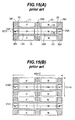
- FIG. 15(A) is a top view of another prior art base cell BCY.
- a gate line 34 serially passes above a channel between P-type diffused regions 11 and 12A and above a channel between N-type diffused regions 21 and 22A and similar to this, a gate line 35 serially passes above a channel between P-type diffused regions 12A and 13 and above a channel between N-type diffused regions 22A and 23.
- a cell pitch of a gate array in a row direction is (8G + G') as shown in FIG. 15(B), and the cell pitch is shorter than that of 10G of FIG. 14(B) by (2G - G').
- 2G - G' 0.6 mm.
- the reason why the cell pitch of the gate array in the row direction is not 9G but (8G + G') is that when cells are arrayed in the row direction, there arises a need to ensure a margin between adjacent gate contact regions, which is required from design rules.
- an N + -type well contact region 16A is formed in the N-type well 10 under a place between gate contact regions 341 and 351 formed at one ends of the gate lines 34 and 35, and similar to this, instead of the P + -type well contact regions 26 and 27 of FIG. 14(A), a P + -type well contact region 26A is formed in the P-type well 20 under a place between gate contact regions 342 and 352 formed at the other ends of the gate lines 34 and 35.
- a semiconductor integrated circuit comprising base cells arrayed in first and second directions perpendicular to each other, each base cell comprising: an N-type well; a plurality of P-type regions formed in the N-type well and arrayed in the second direction; a P-type well arranged adjacent to the N-type well in the first direction; a plurality of N-type regions formed in the P-type well and arrayed in the second direction; gate lines each formed in the first direction passing above a channel between adjacent two of the P-type regions and passing above a channel between adjacent two of the N-type regions, each of the gate lines not having gate contact regions at both ends thereof; an N-type well contact region formed in the N-type well on a side of a first directional end of one of the gate lines; a P-type well contact region formed in the P-type well on a side of an opposite first directional end of one of the gate lines; an intra-cell interconnection formed in a first wiring layer; a first power
- the power supply lines are formed in the second direction, interconnections between base cells in the second direction can be performed using the second wiring layer and automatic interconnection ratio can be increased. Thereby, a higher integration can be achieved.
- FIG. 1(A) is a top view of a base cell BC0 of a first embodiment according to the present invention.
- P-type diffused regions 11 to 13 are arrayed in a column direction in an N-type well 10 indicated with a double dot and dash line
- N-type diffused regions 21 to 23 are arrayed in a column direction in a P-type well 20 indicated with a double dot and dash line, next to the N-type well 10.
- a gate line 34A passes above a channel between the P-type diffused regions 11 and 12 and above a channel between the N-type diffused regions 21 and 22, while a gate line 35A passes above a channel between the P-type diffused regions 12 and 13 and above a channel between the N-type diffused regions 22 and 23.
- gate contact regions 340 and 350 are formed in the middle portions of the gate lines 34A and 35A.
- the gate contact region 340 is located above a place between the P-type diffused region 11 and the N-type diffused region 21, while the gate contact region 350 is located above a place between the P-type diffused region 13 and the N-type diffused region 23.
- An N + -type well contact region 16B is formed in the N-type well 10 on the side of one ends of the gate lines 34A and 35A, while a P + -type well contact region 26B is formed in the P-type well 20 on the side of the other ends of the gate lines 34A and 35A.
- No gate contact regions are formed at both ends of each of the gate lines 34A and 35B.
- widths of the diffused regions 12 and 22 in a column direction can be narrower than those of the diffused regions 12A and 22A of FIG. 15(A). That is, the widths of the diffused regions 12 and 22 in the column direction are same as those of the other diffused regions.
- a power supply line VDD and a ground line VSS are formed, in a second wiring layer above a first wiring layer, above the N + -type well contact region 16B and the P + -type well contact region 26B and in a column direction.
- the power supply lines VDD and VSS are represented by their center lines drawn with a single dot and dash line for simplicity, and this applies to other figures.
- a base cell BC1 shown in FIG. 1(B) is a modification made to that of FIG. 1 (A), and an N + -type well contact region 16C and a P + -type well contact region 26C are formed in the N-type well 10 and the P-type well 20, respectively, in a column direction and lengths thereof are equal to a length in the column direction of a cell frame.
- the other points are same as those in the base cell BC0 of FIG. 1(A).
- FIG. 1(C) shows a two-input NAND gate having the basic BC1 of FIG. 1(B), interconnections L1, L2 and L3 formed in the first wiring layer, and interlayer contacts C1 to C7 indicated by marks ⁇ [$B!_ ⁇ [(J.
- the interlayer contact C1 is for connecting the P-type diffused region 11 and the conductive line L1
- the interlayer contact C2 is for connecting the N + -type well contact region 16C and for connecting the conductive line L1 and the power supply line VDD thereabove
- the interlayer contact C3 is for connecting the P-type diffused region 13 and the conductive line L1.
- the interlayer contact C4 is for connecting-the P-type diffused region 12 and the conductive line L2, and the interlayer contact C5 is for connecting the N-type diffusion region 21 and the conductive line L2.
- the interlayer contact C6 is for connecting the N-type diffused region 23 and the conductive line L3, and the interlayer contact C7 is for connecting the P + -type well contact region 26C and the conductive line L3 and for connecting the conductive line L3 and the ground line VSS thereabove.
- the interconnections L1 and L3 therebetween are shortened, which increases a degree of freedom of the intra-cell conductive line L2 which is other than the interconnections L1 and L3.
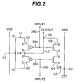
- FIG. 2 is a circuit diagram of the two-input NAND gate drawn in a corresponding manner to the pattern of FIG. 1(C).
- a PMOS transistor Q1 comprises the P-type diffused regions 11 and 12, and the gate line 34A above a channel between the P-type diffused regions 11 and 12, a PMOS transistor Q2 comprises the P-type diffused regions 12 and 13, and the gate line 35A above a channel between the P-type diffused regions 12 and 13, an NMOS transistor Q3 comprises the N-type diffused regions 21 and 22, and the gate line 34A above a channel between the N-type diffused regions 21 and 22, and an NMOS transistor Q4 comprises the N-type diffused regions 22 and 23, and the gate line 35A above a channel between the N-type diffused regions 22 and 23.
- Reference characters S and D in FIG. 2 denote source and drain, respectively, of each transistor.
- Input signals 1 and 2 are provided to the gate contact regions 340 and 350, respectively, and an output signal is taken out from the contact C5.
- FIG. 3 is a top view of an array constructed from base cells, each is same as the cell BC1 of FIG. 1(B), in a matrix of two rows and two columns with adjacent P + -type well contact regions 26C superimposed one on the other in design.
- N + -type well contact regions are also superimposed one on the other in design.
- the power supply lines are formed along the column direction, intra-cell interconnections in the column direction can be implemented using the second wiring layer, which improves a ratio of automatic interconnection. Thereby, a higher integration can be achieved.
- FIG. 4(A) is a top view of a base cell BC2 of a second embodiment according to the present invention.
- the base cell BC2 is obtained by deleting the gate contact regions 351 and 352 of the gate line 35 in the base cell BCY of FIG. 15(A) to form a gate line 35A, and by forming an N + -type well contact region 16B and a P + -type well contact region 26B under the deleted regions in the N-type well 10 and the P-type well 20, respectively.
- an on-chip area of the base cell is reduced compared with the base cell BCY, thereby improving a degree of integration.
- the power supply line VDD and the ground line VSS formed in the second wiring layer above the N + -type well contact region 16B and the P + -type well contact region 26B, respectively, are arranged along a column direction, there can be enjoyed the improvement, as described in the first embodiment, of degree of freedom of intra-cell interconnections and of a ratio of automatic connection in inter-cell interconnections.
- FIG. 4(B) is a top view of an array of two rows and one column having the base cell BC2 of FIG. 4(A) and a cell obtained by vertically flipping the cell of FIG. 4(A). With this flipping, since well contacts adjacent to each other are arrayed in a serial manner, the number of interlayer contacts between the power supply lines and well contact regions decreases, thereby enabling other interlayer contacts to be formed in free spaces saved this way.
- FIG. 5 is a top view of a two-input NAND gate having the base cells of FIG. 4(B), interconnections L1 to L4 formed in the first wiring layer, interlayer contacts C1 to C6 as in FIG. 1(c), and interlayer contacts C71, C72 and C8.
- the interlayer contact C71 is for connecting conductive lines L3 and L4 to the P + -type well contact region 26C thereunder, and the interlayer contact C72 is for connecting the conductive line L4 to the ground line VSS thereabove.
- the interlayer contact C8 is for connecting the power supply line VDD to the N + -type well contact region 16C.
- FIG. 6 is a top view of an array having 2 ⁇ [$B!_ ⁇ [(J2 sub-arrays, each like the array of FIG. 4(B).
- FIG. 7 is a top view of a base cell BC3 which is a modification made to the base cell BC2 of FIG. 4(A).
- the base cell BC3 has an N + -type well contact region 16D and a P + -type well contact region 26D both extending outward in the row direction up to a cell frame.
- the other points are like those of the base cell BC2.
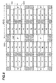
- FIG. 8 is a top view of an array configured such that first sets, each having the base cell of FIG. 7 and a cell obtained by vertically flipping the base cell of FIG. 7, are arrayed in a column direction and second sets obtained by horizontally flipping the first sets are arranged horizontally adjacent to the first sets.
- This array has a pattern 26E which is four times larger than the P + -type well contact region 26D of FIG. 7. Further, since a pattern of the ground line VSS has a twice larger width than that of FIG. 6, an allowable current of the ground line VSS increases, enabling more of stabilization of the power supply potential VSS. This is also applied to the power supply line VDD when a semiconductor integrated circuit has a larger array than that of FIG. 8.
- FIG. 9(A) is a top view of a base cell BC4 of a third embodiment according to the present invention.
- the base cell BC4 is obtained, in the base cell of BCY FIG. 15(A), by deleting the gate contact region 351 of the gate line 35 and the gate contact region 342 of the gate line 34 to form gate lines 35B and 34B, respectively, and by forming an N + -type well contact region 16F and a P + -type well contact region 26F in the N-type well 10 and the P-type well 20, respectively, thereunder.
- an on-chip area of the base cell BC4 is reduced compared with the base cell BCY, leading to increase in degree of integration.
- the power supply line VDD and the ground line VSS formed in the second wiring layer above the N + -type well contact region 16F and the P + -type well contact region 26F, respectively, are arranged along the column direction, there can be enjoyed the improvement, as described in the first embodiment, of degree of freedom of intra-cell interconnections and of a ratio of automatic connection in inter-cell interconnections.
- FIG. 9(B) is a top view of an array of two rows and one column having the base cell BC4 of FIG. 9(A) and a cell obtained by vertically flipping the cell of FIG. 9(A).
- the number of interlayer contacts between the power supply line VDD and N + -type well contact region 16C decreases, thereby enabling other interlayer contacts to be formed in free spaces saved this way.
- FIG. 10 is a top view of a two-input NAND gate having the base cells of FIG. 9(B), interconnections L1 to L4 formed in the first wiring layer and interlayer contacts C1 to C6, C72, C7 and C8, some of which are as in FIG. 1(c).
- the interlayer contact C72 is for connecting the conductive line L3 and the ground line VSS thereabove, and the interlayer contact C7 is for connecting the ground line VSS and the P + -type well contact region 26F.
- the interlayer contact C8 is for connecting the power supply line VDD and the N + -type well contact region 16C thereunder.
- FIG. 11 is a top view of an array having 2 ⁇ [$B!_ ⁇ [(J2 sub-arrays, each is same as the array of FIG. 9(B).
- FIG. 12 is a top view of a base cell BC5 which is a modification made to the base cell BC4 of FIG. 9(A).
- the base cell BC5 has an N + -type well contact region 16G and a P + -type well contact region 26G both extending outward in the row direction up to a cell frame.
- the other points are like those of the base cell BC4.
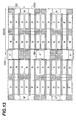
- FIG. 13 is a top view of an array configured such that first sets, each having the base cell BC5 of FIG. 12 and a cell obtained by vertically flipping the base cell of FIG. 12, are arrayed in a column direction and second sets obtained by horizontally flipping the first sets are arranged horizontally adjacent to the first sets.
- This array has a pattern 26H which is four times larger than the P + -type well contact region 26G of FIG. 12. Further, since a pattern of the ground line VSS has a twice larger width than that of FIG. 11, an allowable current of the ground line VSS increases, enabling more of stabilization of the power supply potential VSS. This is also applied to the power supply line VDD when a semiconductor integrated circuit has a larger array than that of FIG. 13.
- an embedded array has a gate array
- the embedded array having the above feature is included in the present invention.
- a semiconductor integrated circuit having the above feature fabricated according to the standard cell method is also included in the present invention.
Landscapes
- Design And Manufacture Of Integrated Circuits (AREA)
- Metal-Oxide And Bipolar Metal-Oxide Semiconductor Integrated Circuits (AREA)
Applications Claiming Priority (2)
| Application Number | Priority Date | Filing Date | Title |
|---|---|---|---|
| JP21713599A JP3647323B2 (ja) | 1999-07-30 | 1999-07-30 | 半導体集積回路 |
| JP21713599 | 1999-07-30 |
Publications (3)
| Publication Number | Publication Date |
|---|---|
| EP1073122A2 true EP1073122A2 (de) | 2001-01-31 |
| EP1073122A3 EP1073122A3 (de) | 2003-11-05 |
| EP1073122B1 EP1073122B1 (de) | 2012-04-04 |
Family
ID=16699413
Family Applications (1)
| Application Number | Title | Priority Date | Filing Date |
|---|---|---|---|
| EP00306522A Expired - Lifetime EP1073122B1 (de) | 1999-07-30 | 2000-07-31 | Integrierter Halbleiterschaltkreis mit Basiszellen-Array hoher Dichte |
Country Status (4)
| Country | Link |
|---|---|
| US (2) | US6603158B1 (de) |
| EP (1) | EP1073122B1 (de) |
| JP (1) | JP3647323B2 (de) |
| KR (1) | KR100568015B1 (de) |
Cited By (1)
| Publication number | Priority date | Publication date | Assignee | Title |
|---|---|---|---|---|
| FR2968128A1 (fr) * | 2010-11-26 | 2012-06-01 | St Microelectronics Sa | Cellule precaracterisee pour circuit intégré |
Families Citing this family (14)
| Publication number | Priority date | Publication date | Assignee | Title |
|---|---|---|---|---|
| JP3526450B2 (ja) * | 2001-10-29 | 2004-05-17 | 株式会社東芝 | 半導体集積回路およびスタンダードセル配置設計方法 |
| JP3997089B2 (ja) | 2002-01-10 | 2007-10-24 | 株式会社ルネサステクノロジ | 半導体装置 |
| JP4620942B2 (ja) * | 2003-08-21 | 2011-01-26 | 川崎マイクロエレクトロニクス株式会社 | 半導体集積回路のレイアウト方法、そのレイアウト構造、およびフォトマスク |
| KR100674956B1 (ko) | 2005-02-12 | 2007-01-26 | 삼성전자주식회사 | Esd에 내성을 가지는 프리미티브 셀 |
| JP4912621B2 (ja) * | 2005-06-07 | 2012-04-11 | 富士通株式会社 | 半導体装置及び半導体装置の配線方法 |
| JP4734049B2 (ja) * | 2005-07-06 | 2011-07-27 | 株式会社東芝 | マスタースライス型半導体集積回路装置 |
| JP4791819B2 (ja) * | 2005-12-26 | 2011-10-12 | 東芝マイクロエレクトロニクス株式会社 | スタンダードセルおよびそれを用いたセルライブラリ |
| WO2009037808A1 (ja) * | 2007-09-18 | 2009-03-26 | Panasonic Corporation | 半導体集積回路 |
| JP5126963B2 (ja) * | 2007-12-10 | 2013-01-23 | ルネサスエレクトロニクス株式会社 | 半導体集積回路 |
| JP5366127B2 (ja) | 2008-11-28 | 2013-12-11 | スパンション エルエルシー | アナログ集積回路 |
| JP5550444B2 (ja) * | 2010-05-17 | 2014-07-16 | ルネサスエレクトロニクス株式会社 | 半導体装置の製造方法 |
| US10133149B2 (en) | 2015-11-25 | 2018-11-20 | Massachusetts Institute Of Technology | Apparatus and methods for generating nonlinear effects in centrosymmetric materials |
| JP7449697B2 (ja) * | 2019-02-06 | 2024-03-14 | ローム株式会社 | 半導体集積回路装置 |
| US12599036B2 (en) * | 2022-04-15 | 2026-04-07 | Arm Limited | Circuit architecture in multi-dimensional monolithic structure |
Family Cites Families (38)
| Publication number | Priority date | Publication date | Assignee | Title |
|---|---|---|---|---|
| JPS5890758A (ja) * | 1981-11-25 | 1983-05-30 | Mitsubishi Electric Corp | 相補形集積回路装置 |
| US4513307A (en) * | 1982-05-05 | 1985-04-23 | Rockwell International Corporation | CMOS/SOS transistor gate array apparatus |
| DE3477312D1 (de) * | 1983-07-09 | 1989-04-20 | Fujitsu Ltd | Masterslice semiconductor device |
| US4570176A (en) * | 1984-04-16 | 1986-02-11 | At&T Bell Laboratories | CMOS Cell array with transistor isolation |
| JPS62150740A (ja) * | 1985-12-25 | 1987-07-04 | Hitachi Ltd | 半導体集積回路装置 |
| JPS62263653A (ja) * | 1986-05-12 | 1987-11-16 | Hitachi Ltd | 半導体集積回路装置の製造方法 |
| US4884115A (en) * | 1987-02-27 | 1989-11-28 | Siemens Aktiengesellschaft | Basic cell for a gate array arrangement in CMOS Technology |
| US4851892A (en) * | 1987-09-08 | 1989-07-25 | Motorola, Inc. | Standard cell array having fake gate for isolating devices from supply voltages |
| US5055716A (en) * | 1990-05-15 | 1991-10-08 | Siarc | Basic cell for bicmos gate array |
| US5079614A (en) * | 1990-09-26 | 1992-01-07 | S-Mos Systems, Inc. | Gate array architecture with basic cell interleaved gate electrodes |
| JP3266644B2 (ja) * | 1991-04-08 | 2002-03-18 | テキサス インスツルメンツ インコーポレイテツド | ゲートアレイ装置 |
| JP2821063B2 (ja) * | 1991-07-18 | 1998-11-05 | 富士通株式会社 | 半導体集積回路装置 |
| JP3060673B2 (ja) * | 1991-11-13 | 2000-07-10 | 日本電気株式会社 | 半導体集積回路 |
| JPH05198680A (ja) * | 1992-01-20 | 1993-08-06 | Nec Ic Microcomput Syst Ltd | 半導体集積回路装置 |
| US5298773A (en) * | 1992-08-17 | 1994-03-29 | United Technologies Corporation | Silicon-on-insulator H-transistor layout for gate arrays |
| JPH06196666A (ja) * | 1992-12-24 | 1994-07-15 | Kawasaki Steel Corp | マスタースライス型半導体集積回路 |
| JPH06196668A (ja) * | 1992-12-24 | 1994-07-15 | Kawasaki Steel Corp | マスタースライス型半導体集積回路 |
| US5420447A (en) * | 1993-01-29 | 1995-05-30 | Sgs-Thomson Microelectronics, Inc. | Double buffer base gate array cell |
| US5536955A (en) * | 1993-03-29 | 1996-07-16 | Toppan Electronics (Usa) Inc. | Electronic devices for use in generating integrated circuit structures and method therefor |
| US5691218A (en) * | 1993-07-01 | 1997-11-25 | Lsi Logic Corporation | Method of fabricating a programmable polysilicon gate array base cell structure |
| JP3144967B2 (ja) * | 1993-11-08 | 2001-03-12 | 株式会社日立製作所 | 半導体集積回路およびその製造方法 |
| US5416431A (en) * | 1994-03-21 | 1995-05-16 | At&T Corp. | Integrated circuit clock driver having improved layout |
| JPH07297290A (ja) * | 1994-04-26 | 1995-11-10 | Fujitsu Ltd | 半導体集積回路装置 |
| JP2747223B2 (ja) * | 1994-06-27 | 1998-05-06 | 日本電気アイシーマイコンシステム株式会社 | 半導体集積回路 |
| JPH0997885A (ja) * | 1995-09-28 | 1997-04-08 | Denso Corp | ゲートアレイ |
| US5723883A (en) * | 1995-11-14 | 1998-03-03 | In-Chip | Gate array cell architecture and routing scheme |
| JPH09253306A (ja) * | 1996-03-19 | 1997-09-30 | Nikon Corp | 振動アクチュエータを備えた記録媒体処理装置及びカード式パチンコ機 |
| JPH1056162A (ja) * | 1996-05-24 | 1998-02-24 | Toshiba Corp | 半導体集積回路およびその設計方法 |
| JP2798056B2 (ja) * | 1996-05-30 | 1998-09-17 | 日本電気株式会社 | マスタスライス半導体集積回路 |
| JPH1074843A (ja) * | 1996-06-28 | 1998-03-17 | Toshiba Corp | 多電源集積回路および多電源集積回路システム |
| JP3701756B2 (ja) * | 1996-11-26 | 2005-10-05 | 株式会社ルネサステクノロジ | 半導体装置 |
| JP3180700B2 (ja) * | 1997-02-03 | 2001-06-25 | 日本電気株式会社 | 半導体集積回路装置 |
| US5932900A (en) * | 1997-06-20 | 1999-08-03 | Faraday Technology Corporation | Flexible cell for gate array |
| US6177691B1 (en) * | 1997-06-30 | 2001-01-23 | Synopsys, Inc. | Cell based array having compute drive ratios of N:1 |
| JPH1154632A (ja) * | 1997-08-01 | 1999-02-26 | Mitsubishi Electric Corp | メモリセルのレイアウトパターン |
| JP4212140B2 (ja) * | 1998-04-09 | 2009-01-21 | シャープ株式会社 | ゲートアレイ |
| JP3257525B2 (ja) * | 1998-10-20 | 2002-02-18 | 日本電気株式会社 | 半導体集積回路装置 |
| JP2001015719A (ja) * | 1999-06-29 | 2001-01-19 | Mitsubishi Electric Corp | ゲートアレイ |
-
1999
- 1999-07-30 JP JP21713599A patent/JP3647323B2/ja not_active Expired - Fee Related
-
2000
- 2000-07-24 KR KR1020000042464A patent/KR100568015B1/ko not_active Expired - Fee Related
- 2000-07-27 US US09/624,391 patent/US6603158B1/en not_active Expired - Lifetime
- 2000-07-31 EP EP00306522A patent/EP1073122B1/de not_active Expired - Lifetime
-
2003
- 2003-06-12 US US10/459,467 patent/US6881989B2/en not_active Expired - Lifetime
Non-Patent Citations (1)
| Title |
|---|
| None |
Cited By (2)
| Publication number | Priority date | Publication date | Assignee | Title |
|---|---|---|---|---|
| FR2968128A1 (fr) * | 2010-11-26 | 2012-06-01 | St Microelectronics Sa | Cellule precaracterisee pour circuit intégré |
| US8963210B2 (en) | 2010-11-26 | 2015-02-24 | Stmicroelectronics Sa | Standard cell for integrated circuit |
Also Published As
| Publication number | Publication date |
|---|---|
| EP1073122B1 (de) | 2012-04-04 |
| JP3647323B2 (ja) | 2005-05-11 |
| US6603158B1 (en) | 2003-08-05 |
| KR100568015B1 (ko) | 2006-04-07 |
| KR20010029998A (ko) | 2001-04-16 |
| EP1073122A3 (de) | 2003-11-05 |
| US6881989B2 (en) | 2005-04-19 |
| US20030209733A1 (en) | 2003-11-13 |
| JP2001044397A (ja) | 2001-02-16 |
Similar Documents
| Publication | Publication Date | Title |
|---|---|---|
| EP1073122B1 (de) | Integrierter Halbleiterschaltkreis mit Basiszellen-Array hoher Dichte | |
| JP3154411B2 (ja) | Cadによってレイアウトされた2金属層集積回路ゲート・アレイ | |
| USRE39469E1 (en) | Semiconductor integrated circuit with mixed gate array and standard cell | |
| US4811073A (en) | Gate array arrangement | |
| US4851892A (en) | Standard cell array having fake gate for isolating devices from supply voltages | |
| US5814844A (en) | Gate array having highly flexible interconnection structure | |
| EP0133958B1 (de) | "Master-Slice"-Halbleiteranordnung | |
| US6271548B1 (en) | Master slice LSI and layout method for the same | |
| US4611236A (en) | Masterslice semiconductor device | |
| US4816887A (en) | CMOS gate array with orthagonal gates | |
| US6269466B1 (en) | Method of constructing an integrated circuit utilizing multiple layers of interconnect | |
| US6675361B1 (en) | Method of constructing an integrated circuit comprising an embedded macro | |
| US4525809A (en) | Integrated circuit | |
| US4750027A (en) | Master slice semiconductor device | |
| US4999698A (en) | Interconnection arrangement for a gate array | |
| US5229629A (en) | Semiconductor integrated circuit having improved cell layout | |
| US3983619A (en) | Large scale integrated circuit array of unit cells and method of manufacturing same | |
| US4682201A (en) | Gate array cell | |
| US6057225A (en) | Semiconductor integrated circuit device having fundamental cells and method of manufacturing the semiconductor integrated circuit device using the fundamental cells | |
| JPH0558582B2 (de) | ||
| US6069373A (en) | Compact semiconductor device using SOI•CMOS technology | |
| GB2221090A (en) | Semiconductor devices | |
| KR960008732B1 (ko) | 게이트 어레이(Gate array) 및 그것을 사용한 반도체 집적회로장치의 제조방법 | |
| JP2839722B2 (ja) | 集積回路装置 | |
| KR900002909B1 (ko) | 반도체 집적 회로 |
Legal Events
| Date | Code | Title | Description |
|---|---|---|---|
| PUAI | Public reference made under article 153(3) epc to a published international application that has entered the european phase |
Free format text: ORIGINAL CODE: 0009012 |
|
| AK | Designated contracting states |
Kind code of ref document: A2 Designated state(s): AT BE CH CY DE DK ES FI FR GB GR IE IT LI LU MC NL PT SE |
|
| AX | Request for extension of the european patent |
Free format text: AL;LT;LV;MK;RO;SI |
|
| PUAL | Search report despatched |
Free format text: ORIGINAL CODE: 0009013 |
|
| AK | Designated contracting states |
Kind code of ref document: A3 Designated state(s): AT BE CH CY DE DK ES FI FR GB GR IE IT LI LU MC NL PT SE |
|
| AX | Request for extension of the european patent |
Extension state: AL LT LV MK RO SI |
|
| 17P | Request for examination filed |
Effective date: 20031222 |
|
| AKX | Designation fees paid |
Designated state(s): DE GB |
|
| 17Q | First examination report despatched |
Effective date: 20060710 |
|
| RAP1 | Party data changed (applicant data changed or rights of an application transferred) |
Owner name: FUJITSU MICROELECTRONICS LIMITED |
|
| RAP1 | Party data changed (applicant data changed or rights of an application transferred) |
Owner name: FUJITSU SEMICONDUCTOR LIMITED |
|
| GRAP | Despatch of communication of intention to grant a patent |
Free format text: ORIGINAL CODE: EPIDOSNIGR1 |
|
| GRAS | Grant fee paid |
Free format text: ORIGINAL CODE: EPIDOSNIGR3 |
|
| GRAA | (expected) grant |
Free format text: ORIGINAL CODE: 0009210 |
|
| AK | Designated contracting states |
Kind code of ref document: B1 Designated state(s): DE GB |
|
| REG | Reference to a national code |
Ref country code: GB Ref legal event code: FG4D |
|
| RIN1 | Information on inventor provided before grant (corrected) |
Inventor name: OSAJIMA, TORU Inventor name: KAJII, YOSHIO |
|
| REG | Reference to a national code |
Ref country code: DE Ref legal event code: R096 Ref document number: 60047046 Country of ref document: DE Effective date: 20120531 |
|
| PLBE | No opposition filed within time limit |
Free format text: ORIGINAL CODE: 0009261 |
|
| STAA | Information on the status of an ep patent application or granted ep patent |
Free format text: STATUS: NO OPPOSITION FILED WITHIN TIME LIMIT |
|
| 26N | No opposition filed |
Effective date: 20130107 |
|
| GBPC | Gb: european patent ceased through non-payment of renewal fee |
Effective date: 20120731 |
|
| PG25 | Lapsed in a contracting state [announced via postgrant information from national office to epo] |
Ref country code: GB Free format text: LAPSE BECAUSE OF NON-PAYMENT OF DUE FEES Effective date: 20120731 |
|
| REG | Reference to a national code |
Ref country code: DE Ref legal event code: R097 Ref document number: 60047046 Country of ref document: DE Effective date: 20130107 |
|
| REG | Reference to a national code |
Ref country code: DE Ref legal event code: R082 Ref document number: 60047046 Country of ref document: DE Representative=s name: REICHERT & LINDNER PARTNERSCHAFT PATENTANWAELT, DE |
|
| REG | Reference to a national code |
Ref country code: DE Ref legal event code: R081 Ref document number: 60047046 Country of ref document: DE Owner name: SOCIONEXT INC., YOKOHAMA-SHI, JP Free format text: FORMER OWNER: FUJITSU LTD., KAWASAKI-SHI, KANAGAWA-KEN, JP Effective date: 20120410 Ref country code: DE Ref legal event code: R082 Ref document number: 60047046 Country of ref document: DE Representative=s name: REICHERT & LINDNER PARTNERSCHAFT PATENTANWAELT, DE Effective date: 20150512 Ref country code: DE Ref legal event code: R081 Ref document number: 60047046 Country of ref document: DE Owner name: SOCIONEXT INC., YOKOHAMA-SHI, JP Free format text: FORMER OWNER: FUJITSU SEMICONDUCTOR LIMITED, YOKOHAMA-SHI, KANAGAWA, JP Effective date: 20150512 Ref country code: DE Ref legal event code: R081 Ref document number: 60047046 Country of ref document: DE Owner name: SOCIONEXT INC., YOKOHAMA-SHI, JP Free format text: FORMER OWNER: FUJITSU LIMITED, KAWASAKI-SHI, KANAGAWA, JP Effective date: 20120410 |
|
| PGFP | Annual fee paid to national office [announced via postgrant information from national office to epo] |
Ref country code: DE Payment date: 20160726 Year of fee payment: 17 |
|
| REG | Reference to a national code |
Ref country code: DE Ref legal event code: R119 Ref document number: 60047046 Country of ref document: DE |
|
| PG25 | Lapsed in a contracting state [announced via postgrant information from national office to epo] |
Ref country code: DE Free format text: LAPSE BECAUSE OF NON-PAYMENT OF DUE FEES Effective date: 20180201 |