EP1069602A2 - Verfahren zur Herstellung eines Dünnschicht-Monokristall-Bauelementes, Solarzellen-Modul und Verfahren zur Herstellung derselben - Google Patents
Verfahren zur Herstellung eines Dünnschicht-Monokristall-Bauelementes, Solarzellen-Modul und Verfahren zur Herstellung derselben Download PDFInfo
- Publication number
- EP1069602A2 EP1069602A2 EP00115248A EP00115248A EP1069602A2 EP 1069602 A2 EP1069602 A2 EP 1069602A2 EP 00115248 A EP00115248 A EP 00115248A EP 00115248 A EP00115248 A EP 00115248A EP 1069602 A2 EP1069602 A2 EP 1069602A2
- Authority
- EP
- European Patent Office
- Prior art keywords
- crystal
- thin
- film single
- solar cell
- film
- Prior art date
- Legal status (The legal status is an assumption and is not a legal conclusion. Google has not performed a legal analysis and makes no representation as to the accuracy of the status listed.)
- Withdrawn
Links
Images


Classifications
-
- H—ELECTRICITY
- H10—SEMICONDUCTOR DEVICES; ELECTRIC SOLID-STATE DEVICES NOT OTHERWISE PROVIDED FOR
- H10P—GENERIC PROCESSES OR APPARATUS FOR THE MANUFACTURE OR TREATMENT OF DEVICES COVERED BY CLASS H10
- H10P90/00—Preparation of wafers not covered by a single main group of this subclass, e.g. wafer reinforcement
- H10P90/19—Preparing inhomogeneous wafers
- H10P90/1904—Preparing vertically inhomogeneous wafers
- H10P90/1906—Preparing SOI wafers
- H10P90/1924—Preparing SOI wafers with separation/delamination along a porous layer
-
- H—ELECTRICITY
- H10—SEMICONDUCTOR DEVICES; ELECTRIC SOLID-STATE DEVICES NOT OTHERWISE PROVIDED FOR
- H10P—GENERIC PROCESSES OR APPARATUS FOR THE MANUFACTURE OR TREATMENT OF DEVICES COVERED BY CLASS H10
- H10P52/00—Grinding, lapping or polishing of wafers, substrates or parts of devices
-
- H—ELECTRICITY
- H10—SEMICONDUCTOR DEVICES; ELECTRIC SOLID-STATE DEVICES NOT OTHERWISE PROVIDED FOR
- H10W—GENERIC PACKAGES, INTERCONNECTIONS, CONNECTORS OR OTHER CONSTRUCTIONAL DETAILS OF DEVICES COVERED BY CLASS H10
- H10W10/00—Isolation regions in semiconductor bodies between components of integrated devices
- H10W10/10—Isolation regions comprising dielectric materials
- H10W10/181—Semiconductor-on-insulator [SOI] isolation regions, e.g. buried oxide regions of SOI wafers
-
- Y—GENERAL TAGGING OF NEW TECHNOLOGICAL DEVELOPMENTS; GENERAL TAGGING OF CROSS-SECTIONAL TECHNOLOGIES SPANNING OVER SEVERAL SECTIONS OF THE IPC; TECHNICAL SUBJECTS COVERED BY FORMER USPC CROSS-REFERENCE ART COLLECTIONS [XRACs] AND DIGESTS
- Y02—TECHNOLOGIES OR APPLICATIONS FOR MITIGATION OR ADAPTATION AGAINST CLIMATE CHANGE
- Y02P—CLIMATE CHANGE MITIGATION TECHNOLOGIES IN THE PRODUCTION OR PROCESSING OF GOODS
- Y02P70/00—Climate change mitigation technologies in the production process for final industrial or consumer products
- Y02P70/50—Manufacturing or production processes characterised by the final manufactured product
-
- Y—GENERAL TAGGING OF NEW TECHNOLOGICAL DEVELOPMENTS; GENERAL TAGGING OF CROSS-SECTIONAL TECHNOLOGIES SPANNING OVER SEVERAL SECTIONS OF THE IPC; TECHNICAL SUBJECTS COVERED BY FORMER USPC CROSS-REFERENCE ART COLLECTIONS [XRACs] AND DIGESTS
- Y10—TECHNICAL SUBJECTS COVERED BY FORMER USPC
- Y10T—TECHNICAL SUBJECTS COVERED BY FORMER US CLASSIFICATION
- Y10T156/00—Adhesive bonding and miscellaneous chemical manufacture
- Y10T156/10—Methods of surface bonding and/or assembly therefor
- Y10T156/1002—Methods of surface bonding and/or assembly therefor with permanent bending or reshaping or surface deformation of self sustaining lamina
- Y10T156/1028—Methods of surface bonding and/or assembly therefor with permanent bending or reshaping or surface deformation of self sustaining lamina by bending, drawing or stretch forming sheet to assume shape of configured lamina while in contact therewith
-
- Y—GENERAL TAGGING OF NEW TECHNOLOGICAL DEVELOPMENTS; GENERAL TAGGING OF CROSS-SECTIONAL TECHNOLOGIES SPANNING OVER SEVERAL SECTIONS OF THE IPC; TECHNICAL SUBJECTS COVERED BY FORMER USPC CROSS-REFERENCE ART COLLECTIONS [XRACs] AND DIGESTS
- Y10—TECHNICAL SUBJECTS COVERED BY FORMER USPC
- Y10T—TECHNICAL SUBJECTS COVERED BY FORMER US CLASSIFICATION
- Y10T156/00—Adhesive bonding and miscellaneous chemical manufacture
- Y10T156/10—Methods of surface bonding and/or assembly therefor
- Y10T156/1002—Methods of surface bonding and/or assembly therefor with permanent bending or reshaping or surface deformation of self sustaining lamina
- Y10T156/1039—Surface deformation only of sandwich or lamina [e.g., embossed panels]
- Y10T156/1041—Subsequent to lamination
-
- Y—GENERAL TAGGING OF NEW TECHNOLOGICAL DEVELOPMENTS; GENERAL TAGGING OF CROSS-SECTIONAL TECHNOLOGIES SPANNING OVER SEVERAL SECTIONS OF THE IPC; TECHNICAL SUBJECTS COVERED BY FORMER USPC CROSS-REFERENCE ART COLLECTIONS [XRACs] AND DIGESTS
- Y10—TECHNICAL SUBJECTS COVERED BY FORMER USPC
- Y10T—TECHNICAL SUBJECTS COVERED BY FORMER US CLASSIFICATION
- Y10T156/00—Adhesive bonding and miscellaneous chemical manufacture
- Y10T156/10—Methods of surface bonding and/or assembly therefor
- Y10T156/1002—Methods of surface bonding and/or assembly therefor with permanent bending or reshaping or surface deformation of self sustaining lamina
- Y10T156/1043—Subsequent to assembly
- Y10T156/1044—Subsequent to assembly of parallel stacked sheets only
- Y10T156/1048—Subsequent to assembly of parallel stacked sheets only to form dished or receptacle-like product
-
- Y—GENERAL TAGGING OF NEW TECHNOLOGICAL DEVELOPMENTS; GENERAL TAGGING OF CROSS-SECTIONAL TECHNOLOGIES SPANNING OVER SEVERAL SECTIONS OF THE IPC; TECHNICAL SUBJECTS COVERED BY FORMER USPC CROSS-REFERENCE ART COLLECTIONS [XRACs] AND DIGESTS
- Y10—TECHNICAL SUBJECTS COVERED BY FORMER USPC
- Y10T—TECHNICAL SUBJECTS COVERED BY FORMER US CLASSIFICATION
- Y10T156/00—Adhesive bonding and miscellaneous chemical manufacture
- Y10T156/10—Methods of surface bonding and/or assembly therefor
- Y10T156/1002—Methods of surface bonding and/or assembly therefor with permanent bending or reshaping or surface deformation of self sustaining lamina
- Y10T156/1043—Subsequent to assembly
- Y10T156/1049—Folding only
Definitions
- the present invention relates to a method of producing thin-film single-crystal devices, solar cell modules, and a method of producing the same.
- the thin-film single-crystal devices include, for example, photoelectric converters such as solar cells and devices for a circuit for driving image display elements such as liquid crystal display elements.
- a solar cell is becoming in common use as an independent source for driving various types of electrical machinery and apparatus or as a source for system interconnection with commercial electric power.
- semiconductors constituting a solar cell silicon and gallium arsenide are generally used. In order to obtain a high photoelectric conversion efficiency (efficiency to convert optical energy into electric power), these semiconductor single-crystals are preferably used.
- a drive circuit formed within an element is required to have much higher capability.
- the drive circuit should be formed on single-crystal silicon rather than amorphous or polycrystal silicon.
- the thickness of the single-crystal wafers commonly used is as thick as about 300 to 600 ⁇ m, while the film thickness required for the absorption of the incident sunlight is about 30 to 50 ⁇ m.
- the single-crystal silicon used in solar cells accounts for ten percent of the total production, its consumption should be reduced.
- image display devices because of the form in which they are used, the light must be transmitted through the areas among the elements in a drive circuit.
- the single-crystal wafers in common use are difficult to have such a structure formed thereon.
- the thickness of a single-crystal layer required for the drive element itself is only 1 ⁇ m or less, the rest portion merely serves as a supporting substrate.
- thin-film single-crystals having a suitable thickness should be selected depending on the purpose for which it is used; however, as long as the prior arts are employed, a single-crystal layer having a thickness of 300 ⁇ m or less is difficult to produce. Specifically, in some methods of prior art, since single-crystal substrates are produced in such a manner as to slice and polish an ingot single-crystal obtained by subjecting a melt of crystal material to crystal growth, single-crystal of 300 ⁇ m or less in thickness are difficult to obtain.
- etching is conducted on the back side of a single-crystal substrate having a thickness of several hundreds ⁇ m; however, a high-quality thin-film single-crystal is considerably difficult to produce by these methods.
- the method disclosed in Japanese Patent Application Laid-Open No. 7-302829 enables the peeling of a thin-film single-crystal from a substrate on which the thin-film single-crystal is epitaxially grown, and a technique disclosed in Japanese Patent Application Laid-Open No.
- 9-331077 enables the peeling of a portion ranging from the surface of a single-crystal substrate to a certain depth, as a thin-film, from the substrate.
- These methods also have a problem that lattice defects may appear in a thin-film single-crystal during the peeling operation, leading to a reduction in quality of the thin-film single-crystal, and in an extreme case, cracks appear in the thin-film single-crystal, leading to a remarkable reduction in production yield.
- effective solutions of the above problems have been desired.
- amorphous silicon solar cells which are formed by depositing an amorphous silicon film on a conductive substrate by the plasma CVD method and forming a transparent conductive layer on the amorphous silicon film, are inexpensive, lightweight, and excellent in impact resistance and flexibility compared with solar cells using crystalline silicon. Making good use of these characteristics, attempts have been made to use an amorphous silicon solar cell as a solar cell incorporated with building materials, that is, as an amorphous silicon solar cell incorporated with roof, wall, etc. of building.
- a solar cell is used as a building material by bonding a reinforcing material to its non-light-receiving side via a bonding agent. Bonding a reinforcing material enhances mechanical strength of a solar cell module and prevents warps and strain, due to changes in temperature.
- This type of solar cell is often installed on a roof because more sunlight can be collected there.
- the installation has been performed as follows: fitting a frame to the solar cell, installing a stand on a roof, and installing the solar cell on the stand.
- the solar cell with a reinforcing material bonded thereto can be directly installed on a roof as a roofing material by bending the reinforcing material. This allows to materially reduce the raw material cost as well as the number of operational steps, and hence to provide a roof with solar cells at a low price.
- the solar cell can be made lightweight since it requires neither frame nor stand.
- the solar cell can be treated as a metal roofing, which has lately attracted considerable attention, due to its excellent workability, lightweight and superior earthquake resistance.
- the solar cell module incorporated with roofing for example, disclosed in Japanese Patent Application Laid-Open No. 7-302924 is excellent in workability since the portions where roof materials engage with each other (the region where photovoltaic elements are not arranged) have been subjected to bending just like ordinary roofing. It is also easy to handle in terms of machining since the current molding machine used for ordinary roofing is applicable as it is. It enables the installation of a roof with solar cells at low costs.
- the solar cell module incorporated with roofing is constructed in such a manner as to be lightweight and machinable like ordinary roofing
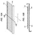
- the most common type of solar cell module incorporated with roofing has a construction in which a photovoltaic element is bonded to or installed on a steel plate (roofing) and subjected to insulation sealing with resin, as shown in Figs. 10A and 10B.
- Figs. 10A and 10B are a schematic perspective view of a plate-type solar cell module incorporated with roofing and a cross-sectional view taken along the line 10B-10B of Fig. 10A, respectively.
- reference numeral 1001 denotes a surface protective material
- numeral 1002 a filler material
- numeral 1003 a photovoltaic element
- numeral 1004 a reinforcing plate.
- An amorphous silicon solar cell module when used as a solar cell module incorporated with roofing described above, has preferable and excellent characteristics, but has problems that its photoelectric conversion efficiency (efficiency to convert optical energy into electric power, hereinafter sometimes refereed to as "conversion efficiency") is generally low compared with that of a crystalline silicon solar cell and its properties may deteriorate due to light (optical deterioration) to some extent when it is used for a long period of time.
- conversion efficiency efficiency to convert optical energy into electric power
- the thickness of the single-crystal wafers commonly used is as thick as about 300 to 600 ⁇ m while the film thickness required for the absorption of incident sunlight is about 30 to 50 ⁇ m. Accordingly, if a single-crystal silicon wafer is used as a photoelectric converting layer as it is, it means single-crystal silicon is needlessly consumed.
- a corrugated solar cell module for example, in Japanese Patent Application Laid-Open No. 8-222752, Japanese Patent Application Laid-Open No. 8-222753 and Japanese Patent Publication No. 6-5769.
- a photovoltaic element is arranged in a corrugated form, and the corrugated solar cell module is produced by following the procedure of bonding a photovoltaic element, with an adhesive agent, to a steel plate previously machined in a corrugated form.
- etching is conducted on the back side of a single-crystal substrate of several hundreds ⁇ m thickness; however, its production process is complicated, and hence under many restrictions.
- a method disclosed in Japanese Patent Application Laid-Open No. 7-302889 enables the peeling of thin-film single-crystal, which is formed on a single-crystal substrate by the epitaxial growth, from the substrate, and a technique disclosed in Japanese Patent Application Laid-Open No. 9-331077 enables the peeling of a portion ranging from the surface of a single-crystal substrate to a certain depth, as a thin film, from the substrate.
- thin-film single-crystal can be molded into a curved surface form to some extent, since it is excellent in flexibility compared with the currently used silicon wafers as described above, although it is inferior to amorphous silicon thin films.
- lattice defects may appear in it, leading to a reduction in its quality, in an extreme case, cracks may appear in the same, leading to a remarkable reduction in its production yield.
- thin-film single-crystal even when thin-film single-crystal is arranged in the region not subjected to bending, it can be momentarily stressed by wind pressure or vibration depending on the circumstances in which it is used, in addition, it can be subjected to bending due to its deformation with lapse of time, and hence to stress. Thus lattice defects may appear in the thin-film single-crystal, leading to a reduction in its quality, in an extreme case, cracks may appear in the same.
- an object of the present invention is to provide, in a case of producing a thin-film single-crystal device, a method of peeling a thin-film single-crystal from a substrate without causing defects and cracks which makes possible to produce a high-quality thin-film single-crystal device in a good yield.
- Another object of the present invention is to provide a high-quality thin-film single-crystal solar cell module which solves the aforementioned problems which arise during the use and production of a solar cell module having a thin-film single-crystal as at least one portion thereof and which is excellent in durability and reliability without defect and crack, and it is to provide a method of producing the module.
- the present invention provides a method of producing a thin-film single-crystal device by utilizing a thin-film single-crystal which is obtained by forming a peeling layer and a thin-film single-crystal on the surface of a substrate in this order, bonding a flexible sheet member to the surface of the above thin-film single-crystal or to the surface of a layer additionally formed on the surface of the above thin-film single-crystal, and peeling the above thin-film single-crystal together with the above sheet member from the substrate by applying force to the above sheet member in such a manner as to curve the sheet member, wherein, the peeling of the thin-film single-crystal from the substrate is carried out in such a manner that the directions of all the straight lines made on the surface of the thin film by the appearance of planes in which the thin-film single-crystal is most apt to cleave are different from the front line of the pealed portion, so as to prevent the generation of defects and cracks.
- the present invention provides a solar cell module with flexibility comprising a photovoltaic element having a thin-film single-crystal as at least one portion thereof, wherein the direction in which the above module is inherently apt to flex is different from the direction in which the above thin-film single-crystal is most apt to cleave.
- the present invention provides a solar cell module with flexibility comprising a photovoltaic element having a thin-film single-crystal as at least one portion thereof, wherein at least one portion of a region having the thin-film single-crystal of the above module is subjected to plastic deformation, and wherein the direction of the plastic deformation is different from to the direction in which the above thin-film single-crystal is most apt to cleave.
- the present invention provides a method of producing a solar cell module with flexibility comprising a photovoltaic element having a thin-film single-crystal as at least one portion thereof, wherein the above thin-film single-crystal is arranged in such a manner that the direction in which the above module is inherently apt to flex is different from the direction in which the above thin-film single-crystal is most apt to cleave.
- the present invention provides a method of producing a solar cell module with flexibility comprising a photovoltaic element having a thin-film single-crystal as at least one portion thereof, which comprises a step of subjecting at least one portion of a region having the thin-film single-crystal of the above module to plastic deformation, wherein the plastic deformation is carried out in such a manner that the direction of the plastic deformation is different from the direction in which the above thin-film single-crystal is most apt to cleave.
- the thin-film single-crystal has the diamond- or zinc blende-type structure.
- the thin-film single-crystal is produced by forming a peeling layer and a thin-film single-crystal layer on a substrate in this order, bonding a plate-shaped flexible member to the surface of the above thin-film single-crystal layer or to the surface of a layer additionally formed on the above thin-film single-crystal layer, and peeling the above plate-shaped member from the substrate by applying force to the plate-shaped member in such a manner as to curve the plate-shaped member.
- the other suitable methods of producing a thin-film single-crystal according to the present invention include, for example, a method including a polishing step and a method including an etching step.
- the angle between the direction in which thin-film single-crystal is most apt to cleave and any one of or any two of or all of the front line of a peeled portion, the direction in which the module is inherently apt to flex deflect and the direction of plastic deformation is 5 degrees or larger, more preferably 10 degrees or larger.
- the present invention may also be applied to the cases where thin-film single-crystal obtained by polishing or etching a single-crystal substrate is utilized in a solar cell module. Further, the present invention may be applied to thin-film single-crystal devices other than solar cells.
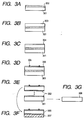
- Figs. 3A to 3E are schematic cross-sectional views illustrating one example of the steps of producing a thin-film single-crystal silicon solar cell.
- a single-crystal silicon wafer is used as a substrate 301.
- a positive electric field is applied to the surface of the substrate while soaking it in hydrofluoric acid solution, so as to form a large number of fine pores irregularly connected to each other in the range of the surface to the depth of several ⁇ m to several tens ⁇ m.
- the region having a large number of fine pores formed in it is referred to as a porous layer 302 (step of Fig. 3A).
- epitaxial growth is conducted by the CVD method or the liquid phase growth method to form a first single-crystal layer 303 (step of Fig. 3B), and a second single-crystal layer 304 is also formed by epitaxial growth (step of Fig. 3C).
- the first single-crystal layer 303 is formed as a weak p type semiconductor (p - type) and the second single-crystal layer 304 is formed as a strong n type semiconductor (n + type).
- the first single-crystal layer 303 and the second single-crystal layer 304 form a pn junction, and the action of the junction causes photovoltage.
- the second single-crystal layer 304 may be formed at the step of Fig. 3C in such a manner as to form a layer containing n type dopant on the first single-crystal layer 303 and subject n type dopant of the layer to thermal diffusion.
- an anti-reflection layer 305 and a grid electrode 306 are formed on the second single-crystal layer 304 in this order (step of Fig. 3D).
- the interior of the porous layer 302 which has become brittle due to the formation of pores, fractures and the upper portion including the first single-crystal layer 303 is peeled from the main part of the substrate 301 (step of Fig. 3E).
- the substrate 301 is illustrated to have the same thickness as those of the single-crystal layers 303 and 304.
- the thickness of the substrate 301 is generally about 600 ⁇ m and far thicker than those of the porous layer 302 or the single-crystal layers 303 and 304. There can sometimes remain residues of the porous layer 302 on the backside of the first single-crystal layer 303 having been peeled, the residues are not necessarily removed.
- a backside electrode 307 is bonded to the backside of the first single-crystal 303 with a conductive adhesive having a high optical reflectance (step of Fig. 3F).
- a conductive adhesive having a high optical reflectance step of Fig. 3F.
- the thin-film single-crystal silicon solar cell is completed.
- the thin-film single-crystal silicon obtained in this manner is extremely of high quality, since it is obtained by conducting the epitaxial growth on a high-quality single-crystal silicon substrate.
- the reclaimed substrate 308 can be reused at the step of Fig. 3A (step of Fig. 3G).
- a costly substrate can be repeatedly used, which enables a significant reduction in manufacturing costs.
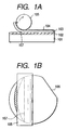
- Fig. 2A is a schematic view showing the state of thin-film single-crystal silicon wafer during peeling
- Fig. 2B is a schematic top view of showing the state during peeling corresponding to Fig. 2A
- Fig. 2C is a plan view of thin-film single-crystal after peeling.
- reference numeral 201 denotes a substrate, numeral 202 a peeling layer, numeral 203 a thin-film single-crystal layer, numeral 204 a sheet member, numeral 205 a peeling roller, numeral 206 a orientation flat, numeral 207 the front line of a peeled portion, numeral 208 a thin-film single-crystal after peeling, and numeral 209 cracks generated in the thin-film single-crystal.
- the peeling layer 202 formed on the substrate 201 can be fractured by applying appropriate force from the outside and it corresponds to the porous layer 302 of Figs. 3A to 3G.
- the thin-film single-crystal layer 203 is formed on this peeling layer.
- the method shown in Figs. 2A and 2B should be employed.
- a flexible plate-shaped member (sheet member) 204 is bonded to the surface of the thin-film single-crystal layer 203.
- Fig. 2A shows that the sheet member 204 is directly bonded to the thin-film single-crystal 203
- the sheet member 204 may be bonded to the surface of a layer such as anti-reflection layer and electrode, additionally formed on the thin-film single-crystal 203, as shown in Figs. 3A to 3G.
- the sheet member 204 or, the adhesive used for bonding the sheet member 204 needs to be transparent or removal afterwards.
- the light may be allowed to enter from the side of the peeling layer 202.
- the sheet member may be opaque, but desirably it is conductive, and suitably a metal sheet is used.
- the peeling layer 202 fractures and the thin-film single-crystal 203 begins to be peeled from the end of the substrate 201.
- This method is suitable for the mass production of solar cells because it can effectively peel the thin-film single-crystal layer 203 from the substrate.
- a solar cell module When being stressed, a solar cell module is inherently apt to in a certain direction which depends on the shape.
- the direction in which the module is apt to deflect corresponds to or nearly corresponds to the direction in which thin-film single-crystal fixed into the module is apt to cleave, flex and cracks may occur in the thin-film single-crystal due to the flexibility of the module during the construction.
- the module Even after installation of the module, while being used for a long period time, the module may be flexed by the stress due to wind pressure, vibration, etc., and this depends on the circumstances in which it is used.
- the direction in which the module is flexed by the stress due to vibration, etc. corresponds to or nearly corresponds to the direction in which the thin-film single-crystal fixed into the module is apt to cleave, defects and cracks may occur in the thin-film single-crystal after using for a long time.
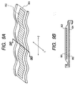
- FIG. 9A is a perspective view of the corrugated solar cell module incorporated with roofing
- Fig. 9B is a cross-sectional view taken along the line 9B-9B of Fig. 9A.
- reference numeral 901 denotes a surface protective material
- numeral 902 a photovoltaic element
- numeral 903 a filler material
- numeral 904 a reinforcing plate.
- FIG. 10A is a perspective view of the plate-shaped solar cell module incorporated with roofing
- Fig. 10B is a cross-sectional view taken along the line 10B-10B of Fig. 10A.
- the photovoltaic element including a thin-film single-crystal layer as at least one portion thereof is arranged on the corrugated portion (curved surface portion) in such a manner that it is curved along the curved surface of the reinforcing plate. Accordingly, the photovoltaic element arranged in the corrugated portion is inevitably stressed in the curved direction (the direction 2) during and after bending.
- the direction 2 corresponds to or nearly corresponds to the direction in which the thin-film single-crystal constituting at least one part of the photovoltaic element is apt to cleave, defects and cracks may gradually occur, for the reasons described above, with the lapse of time while the module is being used for a long period time.
- the present inventors first used various types of silicon wafers as the substrate to form thin-film single-crystal silicon layers and made an experiment to examine conditions of cracking in single-crystal layers under application of strains from various directions so as to bend the thin-film single-crystal layers in the peeling step of the above thin-film single-crystal layers.
- the experimental result is shown in Table 1. Used Plane of Silicon Main Cracking Direction ⁇ 100 ⁇ ⁇ 110 ⁇ ⁇ 110 ⁇ ⁇ 112 ⁇ , ⁇ 110 ⁇ ⁇ 111 ⁇ ⁇ 110 ⁇
- the direction in a crystal is expressed as ⁇ 100 ⁇ .
- ⁇ 100 ⁇ generally represents the [100] direction and those equivalent to the [100] from the symmetry of crystal structures.
- orientation of a crystal face is expressed as ⁇ 100 ⁇ .
- ⁇ 100 ⁇ generally represents the (100) face orientation and those equivalent to the (100) from the symmetry of crystal structures.
- FIG. 1B is a schematic top view showing the situation during peeling, corresponding to Fig. 1A).
- numerals 101 denotes a substrate, 102 a peeling layer, 103 a thin-film single-crystal silicon layer, 104 a sheet member, 105 a peeling roller, 106 orientation flat, and 107 the front line of peeling, respectively.
- the front line 107 of peeling was intentionally deviated from ⁇ 110 ⁇ and cracking hardly occurred in this case.
- a substrate of another face orientation a similar tendency was observed and experiments were made with varying angles between the front line 107 of peeling and the direction of easiest occurring in cleavage. At an angle of not smaller than 5 degrees, the cracking noticeably decreased and hardly occurred at an angle of not smaller than 10 degrees.
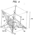
- Fig. 4 is a schematic perspective view showing the unit lattice of a crystal having the diamond type structure.
- a crystal having the diamond type structure shown in Fig. 4 like silicon, the cleavage occurs easily on the ⁇ 111 ⁇ face.
- the direction in which the ⁇ 111 ⁇ face comes to appear for the wafer is that of easily cracking and it is only necessary to perform the peeling so as to deviate the front line 107 of peeling from the direction of easily cracking.
- numerals 401 denotes an atom on the surface of a lattice
- 402 an atom inside a lattice
- 403 a lattice constant
- 404 a covalent bond
- numerals 406 and 407 denote the ⁇ 111 ⁇ face, which is the easiest in cleavage
- numeral 405 denotes the ⁇ 100 ⁇ face.
- the ⁇ 111 ⁇ face 407 appears as the straight line directing as designated with numeral 408 ( ⁇ 110 ⁇ direction).
- Fig. 5A is a view of a wafer 501 cut along the ⁇ 100 ⁇ face ( ⁇ 100 ⁇ wafer) viewed from above, where numeral 502 denotes an orientation flat ⁇ 110 ⁇ , and 503 the ⁇ 110 ⁇ direction.
- the front line of peeling has only to slant to this direction by 5 degrees or greater and preferably by 10 degrees or greater. Since there are two directions equivalent to ⁇ 110 ⁇ , however, a preferable direction for the front line of peeling finally becomes as designated with the angle 504 of a difficulty in cracking.
- Fig. 5A is a view of a wafer 501 cut along the ⁇ 100 ⁇ face ( ⁇ 100 ⁇ wafer) viewed from above, where numeral 502 denotes an orientation flat ⁇ 110 ⁇ , and 503 the ⁇ 110 ⁇ direction.
- the front line of peeling has only to slant to this direction by 5 degrees or greater and preferably by 10 degrees or greater. Since there are two directions equivalent to ⁇ 110 ⁇ , however, a preferable direction for the front line
- numeral 406 denotes a ⁇ 111 ⁇ face equivalent to the face 407.
- the ⁇ 111 ⁇ face 407 appears as the straight line directing as designated with numeral 409 ( ⁇ 110 ⁇ direction).
- numeral 408 there are faces equivalent to the ⁇ 111 ⁇ face and three types of straight lines are designated with numeral 408, any of which is expressed in terms of ⁇ 110 ⁇ .
- Fig. 5B is a schematic view of a wafer cut along the face ⁇ 111 ⁇ ( ⁇ 111 ⁇ wafer) viewed from above, where numeral 506 denotes an orientation flat ⁇ 110 ⁇ , and 507 a direction of ⁇ 110 ⁇ .
- the front line of peeling preferably directs as designated with the angle 508 of a difficulty in cracking.
- Fig. 6 is a schematic view of a zinc-blende type structure semiconductor wafer 601 ( ⁇ 100 ⁇ wafer) cut along ⁇ 100 ⁇ viewed from above, where numerals 602 and 603 denote an orientation flat ⁇ 100 ⁇ and a direction of ⁇ 100 ⁇ , respectively.
- the front line of peeling preferably directs as designated with the angle 604 of a difficulty in cracking.
- FIGs. 7A and 7B are schematic views of one example of a peeling step other than the above, where Fig. 7A is a schematic sectional view showing a situation during the peeling and Fig. 7B is a schematic top view of the situation during the peeling corresponding to Fig. 7A.
- numeral 701 denotes a substrate, 702 a thin-film single-crystal layer, 703 a quartz glass support plate, 704 a peeling wedge, 705 a front edge removed part, 706 a taper part and a front of peeling, respectively.
- a portion of the thin-film single-crystal layer (front end removed portion 705) is removed beforehand by the etching or the like, a quartz glass support plate 703 with the taper part 706 is glued onto it and the thin-film single-crystal layer 702 is peeled from the substrate 701 by driving a peeling wedge 704 from the side of the front end removed part 705.
- the thin-film single-crystal layer 702 is directly provided on the substrate 701, but a peeling layer may be provided between them to drive a wedge 704 there.
- the effect of the present invention can be obtained by deviating the front line 707 of peeling from the direction in which the thin-film single-crystal layer 702 is apt to cleave.
- the thin-film single-crystal is greatly excellent in flexibility in contrast to a conventional crystal substrate, but cracking may occur depending on a bending stress and further this ease of cracking was found to strongly correlate with the direction of stress application. Thus, it was found that by controlling the direction of a stress applied to a thin-film single-crystal, the flexibility of the thin-film single-crystal can be utilized more effectively.
- the effect of the present invention can be obtained by disposing this thin-film single-crystal so as not to make its easiest cleaving direction coincident with the bending easy direction peculiar to the module, not only for the one prepared by peeling as mentioned above but also for the one is obtained by the grinding step or by the etching step.
- This example is an example of the present invention applied to the manufacturing of a thin-film single-crystal silicon solar cell shown in Figs. 3A to 3G.
- a p + silicon wafer 301 of the face orientation ⁇ 111 ⁇ is dipped into a liquid mixture of hydrofluoric acid and isopropyl alcohol (liquid mixture of 49 % by weight of hydrofluoric acid (balance: water) and 99.9 % pure isopropyl alcohol; volume ratio: 1: 0.1), and anodization was carried out with this wafer 301 employed for the positive electrode and a platinum plate employed for the negative electrode.
- a 70 nm thick silicon nitride layer was deposited as the anti-reflection layer 305 by the sputtering. Furthermore, a through hole was formed on this surface and a grid electrode 306 was formed by the printing, onto which a 0.2 mm thick PET film was glued as a sheet member 104 as shown in Fig. 1A by using EVA for the adhesive layer (not shown).
- This sheet member was seized at its end with a 100 mm diameter peeling roller 105 and rolled up from the periphery. At this time, it was rolled up with attention paid to the position of seizing the sheet member and to the direction of the shaft of the peeling roller 105 so that this shaft always directs at an angle of 45 degrees to the orientation flat 106 (orientation: ⁇ 110 ⁇ ) of a wafer. Together with this, the thin-film single-crystal silicon began to be peeled at the part of the porous layer 302. At that time, the direction of the front line 107 of peeling was parallel to that of the shaft of the peeling roller 105. After the roll-up was continued as it was, the whole thin-film single-crystal silicon layer was peeled from the substrate.
- a back electrode 307 of stainless steel plate was glued using a conductive adhesive containing copper as a main component.
- a conversion efficiency of 15 % was obtained.
- the conversion efficiency amounted to 14.0 % under environments comprising a temperature of 45°C and a humidity of 85 %, which value was sufficiently equal to practical use.
- the porous layer residue remaining on the wafer surface dissolved and disappeared and the surface of the reclaimed substrate (wafer) 308 became a mirror surface.
- the solar cell obtained by repetition of the above steps using this wafer also manifested a conversion efficiency of 14.8 %, thereby revealing the repetitive usability of a wafer.
- This example is an example of the present invention applied to the manufacturing of a solar cell using a thin-film single-crystal GaAs.
- a p-type GaAs wafer of the face orientation ⁇ 100 ⁇ was prepared.
- a 0.1 ⁇ m thick n + -type GaAs layer was epitaxially grown in a liquid phase growth apparatus using a melt formed by dissolving arsenic and traces of silicon in a solvent of gallium. Thereafter, to the surface of this wafer, 5 ⁇ 10 16 /cm 2 of hydrogen ions were implanted at an acceleration voltage of 500 keV. Then, on this surface, a 70 nm thick silicon nitride layer was formed as the anti-reflection layer.
- the substrate temperature was set to 450°C.
- a grid electrode was formed by printing, onto which a 0.3 mm thick polycarbonate film was glued as such a sheet member 104 as shown in Fig. 1A by using an acryl adhesive as the adhesive layer (not shown).
- This sheet member was seized at its end with a 100 mm diameter peeling roller 105 and rolled up from the periphery. At this time, it was rolled up with attention paid to the position of seizing the sheet member and to the direction of the shaft of the peeling roller 105 so that this shaft always directs at an angle of 45 degrees to the orientation flat 106 (oriented in ⁇ 100 ⁇ ) of a wafer. Together with this, the single-crystal layer began to be peeled at a depth of 5 ⁇ m from the surface of the single-crystal GaAs wafer.
- the thin-film single-crystal GaAs with a portion of thickness of 5 ⁇ m apart from the surface and the GaAs epitaxial growth layer stacked thereon was peeled from the substrate.
- a back electrode of stainless steel plate was glued using a conductive adhesive containing copper as a main component.
- a conversion efficiency of 18 % was obtained.
- the wafer after the completion of peeling was dipped into fluoronitric acid etching liquid, the wafer surface became a mirror surface.
- the solar cell obtained by repetition of the above steps using this wafer also manifested a conversion efficiency of 17.5 %, thereby revealing the repetitive usability of a wafer.
- This example is an example of the present invention applied to the production of an image display element member with a thin-film single-crystal layer for forming an optically transparent driving circuit which is glued to quartz glass.
- a p + silicon wafer of the face orientation ⁇ 100 ⁇ was dipped into a liquid mixture of hydrofluoric acid and isopropyl alcohol (liquid mixture of 49 % by weight of hydrofluoric acid (balance: water) and 99.9 % pure isopropyl alcohol with a volume ratio of 1: 0.1) and anodization was carried out with this wafer employed for the positive electrode and a platinum plate employed for the negative electrode.
- this wafer employed for the positive electrode and a platinum plate employed for the negative electrode.
- 0.5 ⁇ m thick p-type thin-film single-crystal layer was epitaxially grown using trichlorosilane (SiHCl 3 ) at a substrate temperature of 1000°C by the thermal CVD process. Thereafter, the surface of this thin-film single-crystal was fully cleaned, a flexible quartz glass support plate (sheet member) with the surface kept hydrophilic was bonded to the cleaned face by heating and the quartz support plate was strongly adsorbed to the surface of the thin-film single-crystal.
- SiHCl 3 trichlorosilane
- this thin-film single-crystal was peeled from the silicon wafer.
- the silicon wafer is indicated as a substrate 701.
- the back face of this wafer is strongly adsorbed onto a table by a method such as vacuum adsorption or electromagnetic adsorption.
- a peeling wedge 704 was inserted from the left. To make a hold for the insertion, it is allowable to remove the front end of the thin-film single-crystal 702 to form a space (705) by removing the front end or to form a taper part 706 at the front end of the quartz glass support plate 703.
- the thin-film single-crystal layer 702 and the wafer 701 began to be peeled at the part of the porous layer (not shown) of their interface.
- the front line 707 of peeling was so arranged as to make an angle of 45° to the direction ⁇ 110 ⁇ of the wafer.
- the thin-film layer 702 is a perfect single-crystal layer, since the thin film is only 0.5 ⁇ m thick, it can be made optically transparent and its unnecessary part is easily removable after forming a circuit therein, thereby favoring a liquid crystal display element driving circuit to be built in. Moreover, since the wafer can be reclaimed and repetitively used, the production cost can also be reduced.
- This example is an example of the present invention applied to the manufacturing of the thin-film single-crystal silicon solar cell shown in Figs. 3A to 3G.
- a p + silicon wafer 301 of the face orientation ⁇ 111 ⁇ was dipped into a liquid mixture of hydrofluoric acid and isopropyl alcohol, and anodization was carried out with this wafer 301 employed for the positive electrode and a platinum plate employed for the negative electrode.
- minute current application at a current density of 0.8 A/cm 2
- minute pores complexly entangled down to a depth of approx. 5 ⁇ m from the surface were formed to produce a porous layer 302.
- 25 ⁇ m thick p-type thin-film single-crystal layer 303 was epitaxially grown in a liquid phase growth apparatus using a melt formed by dissolving p-type Silicon into a solvent of indium.
- the epitaxial growth was confirmed by the electron beam diffraction method.
- Hall-effect measurements of a thin-film single-crystal layer peeled by a method according to the present invention in this situation that this thin-film single-crystal 303 was of p type.
- On the surface of the p-type thin-film single-crystal layer 303 an approx.
- 0.2 ⁇ m thick n + -type thin-film single-crystal silicon layer 304 was epitaxially grown in a liquid phase growth apparatus using a melt formed by dissolving n + -type silicon into a solvent of tin. On this surface, an approx. 70 nm thick silicon nitride layer was deposited as the anti-reflection layer 305 by the sputtering. After a through hole was formed on this surface, a grid electrode 306 was formed by the printing, onto which a 0.2 mm thick PET film was glued as a sheet member 104 as shown in Fig. 1A by using EVA for the adhesive layer (not shown).
- This sheet member was seized at its end with a 100 mm diameter peeling roller 105 and rolled up from the periphery. At this time, it was rolled up with attention paid to the position of seizing the sheet member and to the direction of the shaft of the peeling roller 105 so that this shaft always directs at an angle of 45 degrees to the orientation flat 106 (oriented in ⁇ 110 ⁇ ) of a wafer. Together with this, the thin-film single-crystal silicon began to be peeled at the part of the porous layer 302. At that time, the direction of the front line 107 of peeling was parallel to that of the shaft of the peeling roller 105. After the roll-up was continued as it was, the whole thin-film single-crystal silicon was peeled from the substrate.
- a back electrode 307 of stainless steel plate was glued using a conductive adhesive containing copper as a main component.
- a solar simulator adjusted to AM 1.5.
- photoelectric conversion efficiencies were measured under environments comprising a temperature of 45°C and a humidity of 85 %. These photoelectric conversion efficiencies were compared. The result was shown in Table 2.
- a solar cell was manufactured as a trial in the same manner as in Example 4 except for a change in the oriented angle of the shaft of a peeling roller relative to the orientation flat 106.
- a roll-up was carried out so as to keep the shaft of a peeling roller always at an angle of 5 degrees to the orientation flat, seemingly no cracking was observed and the photoelectric conversion efficiency took a relative value of 0.96 as well, which exhibited a function equal to practical use but significantly lowered to a relative value of 0.36 under environments comprising a temperature of 45°C and a humidity of 85%. Hardly observable minute defects seemed to be generated.
- an angle of the shaft of a peeling roller relative to the orientation flat 106 was preferably 5 degrees or more and more preferably 10 degrees or more.
- This example is an example of the present invention applied to the manufacturing of a solar cell using a thin-film single-crystal GaAs.
- a p-type GaAs wafer of the face orientation ⁇ 100 ⁇ was prepared.
- a 0.1 ⁇ m thick n + -type GaAs layer was epitaxially grown in a liquid phase growth apparatus using a melt formed by dissolving arsenic and traces of silicon in a solvent of gallium. Thereafter, to the surface of this wafer, 5 ⁇ 10 16 /cm 2 of hydrogen ions were implanted at an acceleration voltage of 500 keV. Then, on this surface, a 70 nm thick silicon nitride layer was formed as the anti-reflection layer.
- the substrate temperature was set to 450°C.
- a grid electrode formed by printing onto which a 0.3 mm thick polycarbonate film was glued as such a sheet member 104 as shown in Fig. 1A by using an acryl-based adhesive as the adhesive layer (not shown).
- This sheet member was seized at its end with a 100 mm diameter peeling roller 105 and rolled up from the periphery. At this time, it was rolled up with attention paid to the position of seizing the sheet member and to the direction of the shaft of the peeling roller 105 so that this shaft always directs at an angle of 45 degrees to the orientation flat 106 (oriented in ⁇ 100 ⁇ ) of a wafer.
- the single-crystal layer began to be peeled at a part of thickness of 5 ⁇ m apart from the surface of the single-crystal GaAs wafer.
- This is attributable to the fact that hydrogen ions were concentrated at a depth of 5 ⁇ m from the surface by implanting hydrogen ions from the surface and aggregated at the time of sputtering of silicon nitride, resulting in the formation of a peeling layer under application of a stress on the crystal structure, and thus the single-crystal layer was peeled at this part on the occasion of further application of an external force. Meanwhile, the direction of the front line 107 of peeling was parallel to that of the shaft of the peeling roller 105.
- the thin-film single-crystal GaAs was peeled as a whole from the substrate.
- a back electrode 307 of stainless steel plate was glued using a conductive adhesive agent containing copper as a main component.
- a conversion efficiency of 18 % was obtained.
- the wafer after the completion of peeling was dipped into fluoronitric acid-based etching solution, the residue of the porous layer remaining on the surface of a wafer dissolved away and the wafer surface became a mirror surface.
- the solar cell obtained by repetition of the above steps using this wafer also manifested a conversion efficiency of 17.5 %, thereby revealing the repetitive usability of a wafer.
- Fig. 8A is a schematic sectional view of a module fabricated in Example 8 and Fig. 8B is a schematic top view thereof.
- numeral 801 denotes a sheet member, 802 a transparent electrode, 803 a solar cell containing a thin-film single-crystal silicon layer, 804 a conductive adhesive, 805 a conductive tag for series connection, 806 a filler, 807 a front surface protective material, 808 an insulating layer, and 809 a backing plate (reinforcing plate), respectively.
- a flat plate type solar cell module as shown in Figs. 10A and 10B and a wave type solar cell module with a curvature stamped as shown in Figs. 9A and 9B were fabricated.
- Example 8 In the same manner as in Example 8 except that a thin-film single-crystal solar cell was arranged so as to keep the direction of bending processing (direction of arrowhead 2 in Fig. 9A) and the easily flexible direction (direction of arrowhead 1 in Fig. 10A) at angles of 0 degree (parallel) to the orientation flat (oriented in ⁇ 110 ⁇ ) 106 of a thin-film single-crystal layer, a flat plate type module and a wave type module were fabricated and estimate was made similarly. The result is shown in Table 3 together with those of Example 8 and Comparative Example 3.
- Example 8 In the same manner as in Example 8 except that a thin-film single-crystal solar cell was arranged so as to keep the direction of bending processing (direction of arrowhead 2 in Fig. 9A: direction of plastic deformation) and the easily flexible direction (direction of arrowhead 1 in Fig. 10A) at angles of 3 degrees to the orientation flat (oriented in ⁇ 110 ⁇ ) 106 of a thin-film single-crystal layer, a flat plate type module and a wave type module were fabricated and estimate was made similarly. The result is shown in Table 3 together with those of Example 8 and Comparative Example 3.
- a solar cell module according to the present invention is found to improve in durability during the manufacturing process and during the stress application by such an arrangement as to deviate the direction of easily cleaving in a thin-film solar cell from the easily flexible direction peculiar to the solar cell module.
- Example 8 Comparative Example 3 and Example 9 solar cell modules were fabricated with a wide variety of angles between the easy cleavage direction of a thin-film single-crystal layer solar cell and the easily flexible direction peculiar to solar cell modules or the plastic deformation angle, and estimate was made similarly to Example 8. As a result, it was confirmed that an excellent effect was obtained when the angle was equal to and greater than 5 degrees and a especially significant effect was obtained when the angle was equal to and greater than 10 degrees.
- a thin-film single-crystal can be repetitively peeled from the substrate as the thin-film single-crystal has high quality, while damages or deteriorations during processing can be also suppressed in case of module formation of thin-film single-crystal solar cells, and a highly durable solar cell module during use can be also manufactured at low cost and good yield.
- the peeling of a thin-film single-crystal from a substrate is carried out in such a manner that the directions of all straight lines made on the surface of the thin-film single-crystal by appearance of planes such as ⁇ 111 ⁇ on which the single-crystal is most apt to cleave are different from the direction of the front line of the peeled single-crystal.
- This thin-film single-crystal is utilized to produce a solar cell and a drive circuit member of an image display element.
- a method is provided which prevents a decrease in quality and yield of the single-crystal layer caused during the peeling step in which the single-crystal layer used for making a semiconductor device is peeled from the substrate as a thin film.
- a solar cell module with flexibility comprising a photovoltaic element having a thin-film single-crystal as at least one portion thereof is made in such a manner that the direction in which the module is inherently apt to flex is different from the direction in which the thin-film single-crystal is most apt to cleave.
- a thin-film single-crystal solar cell module of high quality that is, a thin-film single-crystal solar cell module excellent in durability and reliability, because of no occurrence of defects and cracks in the thin-film single-crystal during its production and use, and a method of producing the same.
Landscapes
- Photovoltaic Devices (AREA)
Applications Claiming Priority (4)
| Application Number | Priority Date | Filing Date | Title |
|---|---|---|---|
| JP11200531A JP2001026500A (ja) | 1999-07-14 | 1999-07-14 | 薄膜単結晶デバイスの製造法 |
| JP20053199 | 1999-07-14 | ||
| JP21718899 | 1999-07-30 | ||
| JP21718899 | 1999-07-30 |
Publications (1)
| Publication Number | Publication Date |
|---|---|
| EP1069602A2 true EP1069602A2 (de) | 2001-01-17 |
Family
ID=26512247
Family Applications (1)
| Application Number | Title | Priority Date | Filing Date |
|---|---|---|---|
| EP00115248A Withdrawn EP1069602A2 (de) | 1999-07-14 | 2000-07-13 | Verfahren zur Herstellung eines Dünnschicht-Monokristall-Bauelementes, Solarzellen-Modul und Verfahren zur Herstellung derselben |
Country Status (4)
| Country | Link |
|---|---|
| US (1) | US6452091B1 (de) |
| EP (1) | EP1069602A2 (de) |
| CN (3) | CN1156919C (de) |
| AU (1) | AU768197B2 (de) |
Cited By (14)
| Publication number | Priority date | Publication date | Assignee | Title |
|---|---|---|---|---|
| WO2002032667A1 (en) * | 2000-10-18 | 2002-04-25 | Katholieke Universiteit Nijmegen | A method for separating a film and a substrate |
| WO2002061851A1 (fr) | 2001-01-31 | 2002-08-08 | Shin-Etsu Handotai Co.,Ltd. | Cellule solaire et son procede de fabrication |
| DE10107405A1 (de) * | 2001-02-14 | 2002-09-12 | Rainer Schork | Direktprozessierbare Halbleiterfolie |
| DE10311893B3 (de) * | 2003-03-18 | 2004-10-28 | Fraunhofer-Gesellschaft zur Förderung der angewandten Forschung e.V. | Verfahren und Vorrichtung zur grossflächigen Herstellung von Solarzellen |
| WO2005106933A1 (en) | 2004-04-28 | 2005-11-10 | Iufc-Hyu | Flexible single-crystal film and method of manufacturing the same |
| EP1863100A1 (de) * | 2006-05-30 | 2007-12-05 | INTERUNIVERSITAIR MICROELEKTRONICA CENTRUM vzw (IMEC) | Verfahren zur Herstellung von dünnen Substraten |
| DE102006037652A1 (de) * | 2006-08-10 | 2008-02-14 | Bayerisches Zentrum für Angewandte Energieforschung ZAE Bayern e.V. | Ausgedehnte Siliziumsubstrate |
| WO2008125098A1 (de) * | 2007-04-17 | 2008-10-23 | Christopher Eisele | Verfahren und vorrichtung zur herstellung von dünnen scheiben oder folien aus halbleiterkörpern |
| US8043936B2 (en) | 2006-09-29 | 2011-10-25 | Semiconductor Energy Laboratory Co., Ltd. | Method for manufacturing semiconductor device |
| US8058083B2 (en) | 2008-11-20 | 2011-11-15 | Semiconductor Energy Laboratory Co., Ltd. | Method for manufacturing flexible semiconductor device |
| US8137417B2 (en) | 2006-09-29 | 2012-03-20 | Semiconductor Energy Laboratory Co., Ltd. | Peeling apparatus and manufacturing apparatus of semiconductor device |
| US8440129B2 (en) | 2007-11-02 | 2013-05-14 | President And Fellows Of Harvard College | Production of free-standing solid state layers by thermal processing of substrates with a polymer |
| FR2997553A1 (fr) * | 2012-10-31 | 2014-05-02 | Soitec Silicon On Insulator | Procede de separation mecanique d'une structure formee de deux substrats monocristallins |
| DE102019135499B3 (de) * | 2019-12-20 | 2021-04-01 | Fraunhofer-Gesellschaft zur Förderung der angewandten Forschung e.V. | Ablöseelement, Ablöseeinheit und Verfahren zum Ablösen einer Halbleiterschicht von einem Substrat |
Families Citing this family (71)
| Publication number | Priority date | Publication date | Assignee | Title |
|---|---|---|---|---|
| US20070122997A1 (en) | 1998-02-19 | 2007-05-31 | Silicon Genesis Corporation | Controlled process and resulting device |
| US6159824A (en) | 1997-05-12 | 2000-12-12 | Silicon Genesis Corporation | Silicon-on-silicon wafer bonding process using a thin film blister-separation method |
| JP2002206168A (ja) | 2000-10-24 | 2002-07-26 | Canon Inc | シリコン系薄膜の形成方法、シリコン系半導体層の形成方法及び光起電力素子 |
| US6816225B2 (en) * | 2001-06-26 | 2004-11-09 | International Business Machines Corporation | LCD cell construction by mechanical thinning of a color filter substrate |
| TW554398B (en) * | 2001-08-10 | 2003-09-21 | Semiconductor Energy Lab | Method of peeling off and method of manufacturing semiconductor device |
| DE10162064A1 (de) * | 2001-12-17 | 2003-06-26 | Sunyx Surface Nanotechnologies | Hydrophobe Oberfläche mit einer Vielzahl von Elektroden |
| JP2004140120A (ja) * | 2002-10-16 | 2004-05-13 | Canon Inc | 多結晶シリコン基板 |
| JP2004165394A (ja) * | 2002-11-13 | 2004-06-10 | Canon Inc | 積層型光起電力素子 |
| JP4389447B2 (ja) * | 2003-01-28 | 2009-12-24 | セイコーエプソン株式会社 | 電気光学装置の製造方法 |
| KR20060017771A (ko) * | 2003-05-06 | 2006-02-27 | 캐논 가부시끼가이샤 | 반도체기판, 반도체디바이스, 발광다이오드 및 그 제조방법 |
| JP2004335642A (ja) * | 2003-05-06 | 2004-11-25 | Canon Inc | 基板およびその製造方法 |
| US20050124137A1 (en) * | 2003-05-07 | 2005-06-09 | Canon Kabushiki Kaisha | Semiconductor substrate and manufacturing method therefor |
| JP2004356623A (ja) * | 2003-05-08 | 2004-12-16 | Canon Inc | 積層型光起電力素子及びその製造方法 |
| JP2004335823A (ja) * | 2003-05-09 | 2004-11-25 | Canon Inc | 光起電力素子及び光起電力素子の形成方法 |
| TWI242232B (en) * | 2003-06-09 | 2005-10-21 | Canon Kk | Semiconductor substrate, semiconductor device, and method of manufacturing the same |
| JP2005005509A (ja) * | 2003-06-12 | 2005-01-06 | Canon Inc | 薄膜トランジスタ及びその製造方法 |
| US20050066881A1 (en) * | 2003-09-25 | 2005-03-31 | Canon Kabushiki Kaisha | Continuous production method for crystalline silicon and production apparatus for the same |
| GB0323285D0 (en) * | 2003-10-04 | 2003-11-05 | Koninkl Philips Electronics Nv | Device and method of making a device having a patterned layer on a flexible substrate |
| JP2005135942A (ja) * | 2003-10-28 | 2005-05-26 | Canon Inc | 電極配設方法 |
| US20050132332A1 (en) * | 2003-12-12 | 2005-06-16 | Abhay Sathe | Multi-location coordinated test apparatus |
| NO20040756L (no) * | 2004-02-20 | 2005-08-22 | Renewable Energy Corp | Fremgangsmate og system for a etablere samsvar og sporbarhet mellom vaffere og solceller |
| JP2005336008A (ja) | 2004-05-27 | 2005-12-08 | Canon Inc | シリコン膜の製造方法および太陽電池の製造方法 |
| JP4771510B2 (ja) * | 2004-06-23 | 2011-09-14 | キヤノン株式会社 | 半導体層の製造方法及び基板の製造方法 |
| WO2006012544A2 (en) * | 2004-07-22 | 2006-02-02 | The Board Of Trustees Of The Leland Stanford Junior University | Germanium substrate-type materials and approach therefor |
| JP2006216788A (ja) * | 2005-02-03 | 2006-08-17 | Hitachi Cable Ltd | 半導体レーザー用単結晶ウェハ |
| WO2006106072A1 (en) * | 2005-04-06 | 2006-10-12 | Akzo Nobel N.V. | Process for manufacturing pieces of a foil having an inorganic coating of e. g. tco |
| US7811900B2 (en) | 2006-09-08 | 2010-10-12 | Silicon Genesis Corporation | Method and structure for fabricating solar cells using a thick layer transfer process |
| US8993410B2 (en) | 2006-09-08 | 2015-03-31 | Silicon Genesis Corporation | Substrate cleaving under controlled stress conditions |
| US9362439B2 (en) | 2008-05-07 | 2016-06-07 | Silicon Genesis Corporation | Layer transfer of films utilizing controlled shear region |
| US8293619B2 (en) | 2008-08-28 | 2012-10-23 | Silicon Genesis Corporation | Layer transfer of films utilizing controlled propagation |
| JP5171016B2 (ja) * | 2006-10-27 | 2013-03-27 | キヤノン株式会社 | 半導体部材、半導体物品の製造方法、その製造方法を用いたledアレイ |
| US7763791B2 (en) * | 2006-12-29 | 2010-07-27 | Caterpillar Inc | Thin film with oriented cracks on a flexible substrate |
| US20080264411A1 (en) * | 2007-04-26 | 2008-10-30 | Beranek Gerald D | Solar Collector with Hydrophilic Photocatalytic Coated Protective Pane |
| JP2009016771A (ja) * | 2007-06-08 | 2009-01-22 | Hoya Candeo Optronics株式会社 | ウエハ支持ガラス |
| CN101388417B (zh) * | 2007-09-14 | 2011-06-08 | 鸿富锦精密工业(深圳)有限公司 | 太阳能电池组件 |
| JP2009094144A (ja) * | 2007-10-04 | 2009-04-30 | Canon Inc | 発光素子の製造方法 |
| CN101471214B (zh) * | 2007-12-28 | 2010-06-16 | 中国航天科技集团公司第五研究院第五一〇研究所 | 一种金刚石薄膜太阳能电池及其制备方法 |
| US8030119B2 (en) * | 2008-03-08 | 2011-10-04 | Crystal Solar, Inc. | Integrated method and system for manufacturing monolithic panels of crystalline solar cells |
| US8481357B2 (en) * | 2008-03-08 | 2013-07-09 | Crystal Solar Incorporated | Thin film solar cell with ceramic handling layer |
| US8330126B2 (en) | 2008-08-25 | 2012-12-11 | Silicon Genesis Corporation | Race track configuration and method for wafering silicon solar substrates |
| US20100108130A1 (en) * | 2008-10-31 | 2010-05-06 | Crystal Solar, Inc. | Thin Interdigitated backside contact solar cell and manufacturing process thereof |
| US20100108134A1 (en) * | 2008-10-31 | 2010-05-06 | Crystal Solar, Inc. | Thin two sided single crystal solar cell and manufacturing process thereof |
| US8329557B2 (en) | 2009-05-13 | 2012-12-11 | Silicon Genesis Corporation | Techniques for forming thin films by implantation with reduced channeling |
| US8703521B2 (en) | 2009-06-09 | 2014-04-22 | International Business Machines Corporation | Multijunction photovoltaic cell fabrication |
| US8802477B2 (en) | 2009-06-09 | 2014-08-12 | International Business Machines Corporation | Heterojunction III-V photovoltaic cell fabrication |
| US20110056532A1 (en) * | 2009-09-09 | 2011-03-10 | Crystal Solar, Inc. | Method for manufacturing thin crystalline solar cells pre-assembled on a panel |
| US11271128B2 (en) | 2009-10-23 | 2022-03-08 | Utica Leaseco, Llc | Multi-junction optoelectronic device |
| US20170141256A1 (en) | 2009-10-23 | 2017-05-18 | Alta Devices, Inc. | Multi-junction optoelectronic device with group iv semiconductor as a bottom junction |
| US9502594B2 (en) | 2012-01-19 | 2016-11-22 | Alta Devices, Inc. | Thin-film semiconductor optoelectronic device with textured front and/or back surface prepared from template layer and etching |
| US20150380576A1 (en) * | 2010-10-13 | 2015-12-31 | Alta Devices, Inc. | Optoelectronic device with dielectric layer and method of manufacture |
| JP2012033836A (ja) | 2010-08-03 | 2012-02-16 | Canon Inc | トップゲート型薄膜トランジスタ及びこれを備えた表示装置 |
| JP2012049285A (ja) | 2010-08-26 | 2012-03-08 | Shin Etsu Chem Co Ltd | 太陽電池用基板及び太陽電池 |
| US9178105B2 (en) * | 2010-09-21 | 2015-11-03 | Amberwave Inc. | Flexible monocrystalline thin silicon cell |
| US9021164B2 (en) * | 2012-08-03 | 2015-04-28 | Dell Products L.P. | Near field communication mimic device and method of use |
| US20130056044A1 (en) * | 2011-08-03 | 2013-03-07 | Crystal Solar, Inc. | Photovoltaic module fabrication with thin single crystal epitaxial silicon devices |
| US8679943B2 (en) * | 2011-08-23 | 2014-03-25 | International Business Machines Corporation | Fixed curvature force loading of mechanically spalled films |
| US20130153008A1 (en) * | 2011-12-15 | 2013-06-20 | E I Du Pont De Nemours And Company | Photovoltaic module |
| US11038080B2 (en) | 2012-01-19 | 2021-06-15 | Utica Leaseco, Llc | Thin-film semiconductor optoelectronic device with textured front and/or back surface prepared from etching |
| US9040432B2 (en) * | 2013-02-22 | 2015-05-26 | International Business Machines Corporation | Method for facilitating crack initiation during controlled substrate spalling |
| CN105474355B (zh) | 2013-08-06 | 2018-11-13 | 株式会社半导体能源研究所 | 剥离方法 |
| TWI777433B (zh) | 2013-09-06 | 2022-09-11 | 日商半導體能源研究所股份有限公司 | 發光裝置以及發光裝置的製造方法 |
| US9937698B2 (en) | 2013-11-06 | 2018-04-10 | Semiconductor Energy Laboratory Co., Ltd. | Peeling method and light-emitting device |
| US9064698B1 (en) * | 2014-03-30 | 2015-06-23 | International Business Machines Corporation | Thin-film gallium nitride structures grown on graphene |
| TWI695525B (zh) | 2014-07-25 | 2020-06-01 | 日商半導體能源研究所股份有限公司 | 剝離方法、發光裝置、模組以及電子裝置 |
| TWI624073B (zh) * | 2014-08-29 | 2018-05-11 | 精曜有限公司 | 太陽能模組及太陽能電池 |
| US9578736B2 (en) | 2014-12-23 | 2017-02-21 | International Business Machines Corporation | Patterned metallization handle layer for controlled spalling |
| US9263626B1 (en) | 2015-01-29 | 2016-02-16 | International Business Machines Corporation | Crystalline thin film photovoltaic cell |
| JP6371735B2 (ja) | 2015-04-20 | 2018-08-08 | 東芝メモリ株式会社 | 半導体装置の製造方法 |
| US10259207B2 (en) | 2016-01-26 | 2019-04-16 | Semiconductor Energy Laboratory Co., Ltd. | Method for forming separation starting point and separation method |
| US10490682B2 (en) | 2018-03-14 | 2019-11-26 | National Mechanical Group Corp. | Frame-less encapsulated photo-voltaic solar panel supporting solar cell modules encapsulated within multiple layers of optically-transparent epoxy-resin materials |
| JP7360828B2 (ja) * | 2019-07-02 | 2023-10-13 | キヤノントッキ株式会社 | 磁気吸着機構、蒸着装置、および電子デバイスの製造装置 |
Family Cites Families (19)
| Publication number | Priority date | Publication date | Assignee | Title |
|---|---|---|---|---|
| JPH065769A (ja) | 1992-06-22 | 1994-01-14 | Dainippon Printing Co Ltd | 積層構造のフィルム基材およびこれを用いた電子回路素子搭載用リードフレーム |
| JP2613723B2 (ja) | 1992-10-27 | 1997-05-28 | キヤノン株式会社 | 屋根材一体型太陽電池及びその設置方法 |
| JP3257580B2 (ja) | 1994-03-10 | 2002-02-18 | キヤノン株式会社 | 半導体基板の作製方法 |
| JP3507126B2 (ja) | 1994-04-30 | 2004-03-15 | キヤノン株式会社 | 太陽電池付き横葺き屋根ユニット |
| JPH07302829A (ja) | 1994-05-10 | 1995-11-14 | Hitachi Ltd | 試料移動台 |
| US6107213A (en) * | 1996-02-01 | 2000-08-22 | Sony Corporation | Method for making thin film semiconductor |
| JP2786825B2 (ja) | 1995-02-10 | 1998-08-13 | 司電機産業株式会社 | 太陽電池装置 |
| JP2786826B2 (ja) | 1995-02-10 | 1998-08-13 | 司電機産業株式会社 | 太陽電池装置 |
| JP3397968B2 (ja) * | 1996-03-29 | 2003-04-21 | 信越半導体株式会社 | 半導体単結晶インゴットのスライス方法 |
| JP3628108B2 (ja) | 1996-06-10 | 2005-03-09 | 株式会社イオン工学研究所 | 太陽電池の製造方法 |
| JPH1072910A (ja) | 1996-08-30 | 1998-03-17 | Canon Inc | 横葺き屋根板、屋根材一体型太陽電池、横葺き屋根用継ぎ手及び横葺き屋根の施工方法 |
| JP3347620B2 (ja) | 1996-11-25 | 2002-11-20 | キヤノン株式会社 | 太陽電池 |
| EP0849788B1 (de) * | 1996-12-18 | 2004-03-10 | Canon Kabushiki Kaisha | Vefahren zum Herstellen eines Halbleiterartikels unter Verwendung eines Substrates mit einer porösen Halbleiterschicht |
| EP0851513B1 (de) * | 1996-12-27 | 2007-11-21 | Canon Kabushiki Kaisha | Herstellungsverfahren eines Halbleiter-Bauelements und Herstellungsverfahren einer Solarzelle |
| AU741432B2 (en) * | 1997-04-21 | 2001-11-29 | Canon Kabushiki Kaisha | Solar cell module and method for manufacturing same |
| MY118019A (en) * | 1998-02-18 | 2004-08-30 | Canon Kk | Composite member, its separation method, and preparation method of semiconductor substrate by utilization thereof |
| JP3619058B2 (ja) * | 1998-06-18 | 2005-02-09 | キヤノン株式会社 | 半導体薄膜の製造方法 |
| JP2000252510A (ja) * | 1998-12-28 | 2000-09-14 | Canon Inc | 太陽電池モジュール及びその製造方法、施工方法並びに太陽光発電システム |
| US6664169B1 (en) * | 1999-06-08 | 2003-12-16 | Canon Kabushiki Kaisha | Process for producing semiconductor member, process for producing solar cell, and anodizing apparatus |
-
2000
- 2000-07-12 US US09/614,548 patent/US6452091B1/en not_active Expired - Fee Related
- 2000-07-13 EP EP00115248A patent/EP1069602A2/de not_active Withdrawn
- 2000-07-14 CN CNB001240986A patent/CN1156919C/zh not_active Expired - Fee Related
- 2000-07-14 CN CNA200310114344A patent/CN1505174A/zh active Pending
- 2000-07-14 CN CNA2003101143451A patent/CN1516291A/zh active Pending
- 2000-07-14 AU AU48638/00A patent/AU768197B2/en not_active Ceased
Cited By (27)
| Publication number | Priority date | Publication date | Assignee | Title |
|---|---|---|---|---|
| WO2002032667A1 (en) * | 2000-10-18 | 2002-04-25 | Katholieke Universiteit Nijmegen | A method for separating a film and a substrate |
| US6974521B2 (en) | 2000-10-18 | 2005-12-13 | Katholieke Universiteit Nijmegen | Method for separating a film and a substrate |
| WO2002061851A1 (fr) | 2001-01-31 | 2002-08-08 | Shin-Etsu Handotai Co.,Ltd. | Cellule solaire et son procede de fabrication |
| EP1365455A4 (de) * | 2001-01-31 | 2006-09-20 | Shinetsu Handotai Kk | Solarzelle und verfahren zu ihrer herstellung |
| DE10107405A1 (de) * | 2001-02-14 | 2002-09-12 | Rainer Schork | Direktprozessierbare Halbleiterfolie |
| DE10311893B3 (de) * | 2003-03-18 | 2004-10-28 | Fraunhofer-Gesellschaft zur Förderung der angewandten Forschung e.V. | Verfahren und Vorrichtung zur grossflächigen Herstellung von Solarzellen |
| WO2005106933A1 (en) | 2004-04-28 | 2005-11-10 | Iufc-Hyu | Flexible single-crystal film and method of manufacturing the same |
| EP1751788A4 (de) * | 2004-04-28 | 2010-01-13 | Iucf Hyu | Flexibler einkristallfilm und herstellungsverfahren dafür |
| US8383492B2 (en) | 2006-04-19 | 2013-02-26 | Imec | Method for the production of thin layer of silicon by utilization of mismatch in coefficient of thermal expansion between screen printed metal layer and silicon mother substrate |
| EP1863100A1 (de) * | 2006-05-30 | 2007-12-05 | INTERUNIVERSITAIR MICROELEKTRONICA CENTRUM vzw (IMEC) | Verfahren zur Herstellung von dünnen Substraten |
| DE102006037652A1 (de) * | 2006-08-10 | 2008-02-14 | Bayerisches Zentrum für Angewandte Energieforschung ZAE Bayern e.V. | Ausgedehnte Siliziumsubstrate |
| US8048770B2 (en) | 2006-09-29 | 2011-11-01 | Semiconductor Energy Laboratory Co., Ltd. | Method for manufacturing semiconductor device |
| US9087931B2 (en) | 2006-09-29 | 2015-07-21 | Semiconductor Energy Laboratory Co., Ltd. | Peeling apparatus and manufacturing apparatus of semiconductor device |
| US8048777B2 (en) | 2006-09-29 | 2011-11-01 | Semiconductor Energy Laboratory Co., Ltd. | Method for manufacturing semiconductor device |
| US10134784B2 (en) | 2006-09-29 | 2018-11-20 | Semiconductor Energy Laboratory Co., Ltd. | Peeling apparatus and manufacturing apparatus of semiconductor device |
| US8137417B2 (en) | 2006-09-29 | 2012-03-20 | Semiconductor Energy Laboratory Co., Ltd. | Peeling apparatus and manufacturing apparatus of semiconductor device |
| US9570329B2 (en) | 2006-09-29 | 2017-02-14 | Semiconductor Energy Laboratory Co., Ltd. | Peeling apparatus and manufacturing apparatus of semiconductor device |
| US9397126B2 (en) | 2006-09-29 | 2016-07-19 | Semiconductor Energy Laboratory Co., Ltd. | Peeling apparatus and manufacturing apparatus of semiconductor device |
| US8043936B2 (en) | 2006-09-29 | 2011-10-25 | Semiconductor Energy Laboratory Co., Ltd. | Method for manufacturing semiconductor device |
| US8889438B2 (en) | 2006-09-29 | 2014-11-18 | Semiconductor Energy Laboratory Co., Ltd. | Peeling apparatus and manufacturing apparatus of semiconductor device |
| US9054141B2 (en) | 2006-09-29 | 2015-06-09 | Semiconductor Energy Laboratory Co., Ltd. | Method for manufacturing semiconductor device |
| WO2008125098A1 (de) * | 2007-04-17 | 2008-10-23 | Christopher Eisele | Verfahren und vorrichtung zur herstellung von dünnen scheiben oder folien aus halbleiterkörpern |
| US8440129B2 (en) | 2007-11-02 | 2013-05-14 | President And Fellows Of Harvard College | Production of free-standing solid state layers by thermal processing of substrates with a polymer |
| US8058083B2 (en) | 2008-11-20 | 2011-11-15 | Semiconductor Energy Laboratory Co., Ltd. | Method for manufacturing flexible semiconductor device |
| FR2997553A1 (fr) * | 2012-10-31 | 2014-05-02 | Soitec Silicon On Insulator | Procede de separation mecanique d'une structure formee de deux substrats monocristallins |
| DE102019135499B3 (de) * | 2019-12-20 | 2021-04-01 | Fraunhofer-Gesellschaft zur Förderung der angewandten Forschung e.V. | Ablöseelement, Ablöseeinheit und Verfahren zum Ablösen einer Halbleiterschicht von einem Substrat |
| WO2021121769A1 (de) | 2019-12-20 | 2021-06-24 | Fraunhofer-Gesellschaft zur Förderung der angewandten Forschung e. V. | Ablöseelement und verfahren zum ablösen einer halbleiterschicht von einem substrat |
Also Published As
| Publication number | Publication date |
|---|---|
| AU4863800A (en) | 2001-01-18 |
| CN1283874A (zh) | 2001-02-14 |
| CN1505174A (zh) | 2004-06-16 |
| CN1516291A (zh) | 2004-07-28 |
| CN1156919C (zh) | 2004-07-07 |
| US6452091B1 (en) | 2002-09-17 |
| AU768197B2 (en) | 2003-12-04 |
Similar Documents
| Publication | Publication Date | Title |
|---|---|---|
| US6452091B1 (en) | Method of producing thin-film single-crystal device, solar cell module and method of producing the same | |
| EP1918999B1 (de) | Verfahren zur Herstellung einer einkristallinen Silizium Solarzelle und einkristalline Silizium Solarzelle | |
| US6818104B2 (en) | Anodizing apparatus | |
| EP0849788B1 (de) | Vefahren zum Herstellen eines Halbleiterartikels unter Verwendung eines Substrates mit einer porösen Halbleiterschicht | |
| US8227289B2 (en) | Method for producing single crystal silicon solar cell and single crystal silicon solar cell | |
| JP3271990B2 (ja) | 光起電力素子及びその製造方法 | |
| EP1981092B1 (de) | Verfahren zur Herstellung von einkristallinen Silizium-Solarzellen | |
| US8227290B2 (en) | Method for producing single crystal silicon solar cell and single crystal silicon solar cell | |
| US8101451B1 (en) | Method to form a device including an annealed lamina and having amorphous silicon on opposing faces | |
| US8518724B2 (en) | Method to form a device by constructing a support element on a thin semiconductor lamina | |
| JP4987191B2 (ja) | 集積化薄膜太陽電池の製造方法 | |
| JP5330723B2 (ja) | 光電変換装置 | |
| US6348362B1 (en) | Manufacturing method of photovoltaic device | |
| JP2001026500A (ja) | 薄膜単結晶デバイスの製造法 | |
| JP2001111081A (ja) | 太陽電池モジュール及び太陽電池モジュールの製造方法 | |
| JP4245131B2 (ja) | 薄膜太陽電池の製造方法 | |
| EP2352175A1 (de) | Verfahren zur herstellung eines fotoelektrischen wandlers | |
| US20100167454A1 (en) | Double-sided donor for preparing a pair of thin laminae | |
| JPH11330513A (ja) | 集積型シリコン系薄膜光電変換装置の製造方法 | |
| WO2012092145A2 (en) | A method to form a device by constructing a support element on a thin semiconductor lamina | |
| Wang | Development of a high performance ultra-thin silicon solar cell on steel substrate | |
| JP2001274425A (ja) | 光起電力装置 |
Legal Events
| Date | Code | Title | Description |
|---|---|---|---|
| PUAI | Public reference made under article 153(3) epc to a published international application that has entered the european phase |
Free format text: ORIGINAL CODE: 0009012 |
|
| AK | Designated contracting states |
Kind code of ref document: A2 Designated state(s): AT BE CH CY DE DK ES FI FR GB GR IE IT LI LU MC NL PT SE |
|
| AX | Request for extension of the european patent |
Free format text: AL;LT;LV;MK;RO;SI |
|
| STAA | Information on the status of an ep patent application or granted ep patent |
Free format text: STATUS: THE APPLICATION HAS BEEN WITHDRAWN |
|
| 18W | Application withdrawn |
Effective date: 20060718 |