EP1045418B1 - Protective device - Google Patents
Protective device Download PDFInfo
- Publication number
- EP1045418B1 EP1045418B1 EP00107886A EP00107886A EP1045418B1 EP 1045418 B1 EP1045418 B1 EP 1045418B1 EP 00107886 A EP00107886 A EP 00107886A EP 00107886 A EP00107886 A EP 00107886A EP 1045418 B1 EP1045418 B1 EP 1045418B1
- Authority
- EP
- European Patent Office
- Prior art keywords
- fuse element
- protective device
- point
- fuse
- electrodes
- Prior art date
- Legal status (The legal status is an assumption and is not a legal conclusion. Google has not performed a legal analysis and makes no representation as to the accuracy of the status listed.)
- Expired - Lifetime
Links
Images


Classifications
-
- H—ELECTRICITY
- H01—ELECTRIC ELEMENTS
- H01H—ELECTRIC SWITCHES; RELAYS; SELECTORS; EMERGENCY PROTECTIVE DEVICES
- H01H85/00—Protective devices in which the current flows through a part of fusible material and this current is interrupted by displacement of the fusible material when this current becomes excessive
- H01H85/02—Details
- H01H85/46—Circuit arrangements not adapted to a particular application of the protective device
- H01H85/463—Circuit arrangements not adapted to a particular application of the protective device with printed circuit fuse
-
- H—ELECTRICITY
- H05—ELECTRIC TECHNIQUES NOT OTHERWISE PROVIDED FOR
- H05K—PRINTED CIRCUITS; CASINGS OR CONSTRUCTIONAL DETAILS OF ELECTRIC APPARATUS; MANUFACTURE OF ASSEMBLAGES OF ELECTRICAL COMPONENTS
- H05K1/00—Printed circuits
- H05K1/02—Details
- H05K1/0286—Programmable, customizable or modifiable circuits
- H05K1/0293—Individual printed conductors which are adapted for modification, e.g. fusable or breakable conductors, printed switches
-
- H—ELECTRICITY
- H01—ELECTRIC ELEMENTS
- H01H—ELECTRIC SWITCHES; RELAYS; SELECTORS; EMERGENCY PROTECTIVE DEVICES
- H01H85/00—Protective devices in which the current flows through a part of fusible material and this current is interrupted by displacement of the fusible material when this current becomes excessive
- H01H85/02—Details
- H01H85/46—Circuit arrangements not adapted to a particular application of the protective device
- H01H2085/466—Circuit arrangements not adapted to a particular application of the protective device with remote controlled forced fusing
-
- H—ELECTRICITY
- H01—ELECTRIC ELEMENTS
- H01H—ELECTRIC SWITCHES; RELAYS; SELECTORS; EMERGENCY PROTECTIVE DEVICES
- H01H85/00—Protective devices in which the current flows through a part of fusible material and this current is interrupted by displacement of the fusible material when this current becomes excessive
- H01H85/02—Details
- H01H85/04—Fuses, i.e. expendable parts of the protective device, e.g. cartridges
- H01H85/05—Component parts thereof
- H01H85/055—Fusible members
- H01H85/06—Fusible members characterised by the fusible material
-
- H—ELECTRICITY
- H05—ELECTRIC TECHNIQUES NOT OTHERWISE PROVIDED FOR
- H05K—PRINTED CIRCUITS; CASINGS OR CONSTRUCTIONAL DETAILS OF ELECTRIC APPARATUS; MANUFACTURE OF ASSEMBLAGES OF ELECTRICAL COMPONENTS
- H05K2201/00—Indexing scheme relating to printed circuits covered by H05K1/00
- H05K2201/03—Conductive materials
- H05K2201/0302—Properties and characteristics in general
- H05K2201/0305—Solder used for other purposes than connections between PCB or components, e.g. for filling vias or for programmable patterns
-
- H—ELECTRICITY
- H05—ELECTRIC TECHNIQUES NOT OTHERWISE PROVIDED FOR
- H05K—PRINTED CIRCUITS; CASINGS OR CONSTRUCTIONAL DETAILS OF ELECTRIC APPARATUS; MANUFACTURE OF ASSEMBLAGES OF ELECTRICAL COMPONENTS
- H05K2201/00—Indexing scheme relating to printed circuits covered by H05K1/00
- H05K2201/10—Details of components or other objects attached to or integrated in a printed circuit board
- H05K2201/10007—Types of components
- H05K2201/10181—Fuse
-
- Y—GENERAL TAGGING OF NEW TECHNOLOGICAL DEVELOPMENTS; GENERAL TAGGING OF CROSS-SECTIONAL TECHNOLOGIES SPANNING OVER SEVERAL SECTIONS OF THE IPC; TECHNICAL SUBJECTS COVERED BY FORMER USPC CROSS-REFERENCE ART COLLECTIONS [XRACs] AND DIGESTS
- Y10—TECHNICAL SUBJECTS COVERED BY FORMER USPC
- Y10T—TECHNICAL SUBJECTS COVERED BY FORMER US CLASSIFICATION
- Y10T29/00—Metal working
- Y10T29/49—Method of mechanical manufacture
- Y10T29/49002—Electrical device making
- Y10T29/49107—Fuse making
Definitions
- the present invention relates to a protective device provided with a fuse element on a substrate.
- Protective devices obtained by forming fuse elements on a substrate are known as chip-type electric fuses.
- protective devices in which heating elements are placed in the vicinity of fuse elements are used in overvoltage prevention devices (Japanese Patent No. 2790433, Japanese Patent Application Laid-Open No. 8-161990).
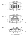
- Figs. 2B and 2C are a plane view and a cross section, respectively, of such a protective device 1o.
- electrodes 3a, 3b, and 3c are formed on a substrate 2, and solder foil spanning the electrodes 3a, 3b, and 3c is provided as a fuse element 4.
- the bottom surface of the electrode 3b is provided with a heating element 7 with an insulating layer 8 sandwiched therebetween. Heating current is supplied to the heating element 7 from an electrode 3o through conductors 3x and 3y.
- the conductors 3x and 3y, heating element 7, insulating layer 8, and electrodes 3a, 3b, and 3c are formed on the substrate 2; solder paste 5 is then applied to the electrodes 3a, 3b, and 3c in the manner shown in Fig. 2A; a fuse element 4 is mounted on top; and a cover (not shown) is provided as needed.
- the protective device 1o thus obtained is commonly heated and mounted on a base circuit board by reflowing, soldering, or a similar technique.
- materials whose solidus point is higher than the mounting temperature of the fuse element 4 are used for the fuse element 4.
- materials whose liquidus points are at or above the temperature maintained during heating and mounting are selected for the solder paste 5.
- the temperature at which the protective device 1o is mounted on a circuit board is set to 250°C
- a material whose liquidus point is 250°C or higher is used for the solder paste 5 of the protective device 1o
- a material whose solidus point is higher than the liquidus point of the solder paste 5 is used for the fuse element 4.
- the above-described protective device 1o When the above-described protective device 1o is used as a protective device in an apparatus to be protected, a malfunction in the apparatus causes an overcurrent to flow through the fuse element 4 and to melt it, or causes the heating current from the electrode 3o to be supplied to the heating element 7 through the conductors 3x and 3y, and the fuse element 4 to be melted by the generated heat.
- a drawback, however, is that the high liquidus point of the fuse element 4 increases the time between the beginning of the increase in the temperature of the fuse element 4 and the melting of the element, resulting in a protective device with an extended operating response.
- An object of the present invention which is aimed at overcoming the above-described drawbacks of prior art, is to improve the operating response, to widen the selection of materials for fuse elements, and to reduce manufacturing costs in a protective device obtained by forming a fuse element on a substrate.
- the protective device of the present invention is obtained by providing a fuse element to electrodes on a substrate.
- the substrate, electrodes, and fuse element are not subject to any particular limitations in terms of shape or arrangement. Consequently, the protective device of the present invention may be constituted as a chip-type current fuse obtained by providing a fuse element to electrodes on a substrate, or as a protective device obtained by further providing a heating element in the vicinity of the fuse element and using the product as an overvoltage prevention device. It is possible, for example, to use the same arrangement as that adopted for the protective device 1o described with reference to Figs. 2A to 2C above.
- the liquidus point should be higher than the predetermined mounting temperature of the protective device, higher than the maximum temperature achieved during mounting.
- the solidus point of the material should be lower than the mounting temperature, preferably lower than the maximum temperature achieved during mounting. This gives a much wider selection of fuse element materials.
- the fuse element starts melting during mounting, and is thus easier to mount on the electrodes when a solder paste is not interposed between the electrodes and the fuse element.
- the fuse element 4 and the electrodes 3a, 3b, and 3c can be securely bonded and a protective device 1 obtained (as shown in Figs.
- solder paste to mount a solder foil of prescribed composition as the fuse element 4 causes this solder foil to melt during reflowing or the like, whereas dispensing with the solder paste overcomes this problem as well.
- the difference between the liquidus and solidus points of the fuse element 4 should be 5°C or higher, and preferably 10°C or higher.
- the difference between the liquidus and solidus points is less than 5°C, it becomes impossible to cope with the commonly encountered nonuniformity of the mounting temperature, and the fuse element occasionally melts. Reducing this nonuniformity prevents the fuse element from melting as a result of the narrow difference between the liquidus and solidus points, but eliminating this nonuniformity is unsuitable because it requires maintaining very stringent conditions for the manufacture of the fuse element 4.
- it suitable for the liquidus point of the fuse element 4 to be more than 50°C above the maximum temperature achieved during mounting, because the operating response of the protective device 1 is adversely affected in this case.
- the material constituting the fuse element 4 having such a liquidus point and a solidus point can be appropriately selected from conventional fuse element materials.
- Sn-Pb solder foil common solder, or the like.
- the component ratio of the material should be adjusted in order to provide the fuse element 4 with prescribed solidus point and liquidus point.
- the liquidus point can be continuously adjusted by varying the Sn and Pb ratio in an appropriate manner.
- a heating element is further provided in the vicinity of the fuse element in order to allow the protective device of the present invention to be used for an overvoltage prevention device as well.
- a fuse element and a heating element are provided in the vicinity of each other includes an embodiment in which a fuse element (low-melting metal element) is stacked on a heating element with an insulating layer sandwiched therebetween as described with reference to Figs. 1A to 1C and Figs. 2A to 2C, as well as in Japanese Patent No. 2790433 and Japanese Patent Application Laid-open No.
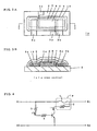
- the protective device 1p shown in Figs. 3A and 3B may be constituted such that a heating element 7 formed by applying or otherwise using a resistive paste, an insulating layer 8, and a fuse element 4 consisting of a fuse material are sequentially stacked on a substrate 2.
- 3x and 3y are heating element electrodes
- 3a and 3b are fuse element electrodes.
- 9 is an internal seal composed of solid flux or the like and designed to cover the fuse element 4 in order to prevent the surface of the fuse element 4 from oxidation
- 10 is an external seal composed of a material whose melting point or softening point is higher than that of the fuse element 4, and designed to prevent molten material from flowing out of the fuse element 4 during the melting of the element.
- Fig. 4 is a circuit diagram of an overvoltage prevention device obtained using such a protective device 1p.
- the electrode terminals of a lithium ion battery or other protected device are connected to terminals A1 and A2, and the electrode terminals of a charger or other device connected to the protected device are connected to terminals B1 and B2.
- base current ib flows abruptly, powerful collector current ic flows through the heating element 7 as a result, and the heating element 7 heats up when a lithium ion battery is charged and a reverse voltage exceeding the breakdown voltage is applied to a Zener diode D. Evolved heat is transmitted to the fuse element 4 on the heating element 7, and the fuse element 4 melts, preventing overvoltage from being applied to the terminals A1 and A2.
- Figs. 5A and 5B are a plane view and a cross section of a protective device 1q constituted differently from the protective device 1p in Figs. 3A and 3B above.
- the protective device 1q two heating elements 7 are connected by means of a middle electrode 3z, and a fuse element 4 is provided thereon with an insulating layer 8 sandwiched therebetween.
- Fig. 6 is a circuit diagram of an overvoltage prevention device obtained using such a protective device 1q.
- the overvoltage prevention device whose circuit is shown in Fig. 4 above is constituted such that the heating element 7 continues to be energized even after the fuse element 4 has been melted by overvoltage
- the overvoltage prevention device whose circuit is shown in Fig. 6 is constituted such that the heat evolved by the heating element 7 melts the fuse element 4 at two locations (4a and 4b), completely preventing the current from flowing through the heating element 7 following such melting.
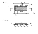
- the protective device 1r in Figs. 7A and 7B is a protective device in which the overvoltage prevention device whose circuit is shown in Fig. 6 can be used. Unlike the protective device 1q in Figs. 5A and 5B, the protective device 1r is designed to provide a sufficiently wide surface area for the heating element 7 or the electrodes 3a and 3b wetted by the molten fuse element 4 during the melting of this element, facilitating melting and making it possible to dispense with the formation of an insulating layer 8 on the heating element 7. Without the insulating layer 8, the heating element 7 has an even shorter operating time.
- solder paste and solder foil shown in Table 1 were used to fabricate a protective device obtained without the use of a solder paste (Figs. 1A to 1C) and a protective device obtained using a solder paste (Figs. 2A to 2C).
- an aluminum substrate (3 mm x 5 mm) was used as the substrate 2, and the solder foil used had the following measurements: 0.15 mm (thickness) x 1.0 mm (width) x 4.2 mm (length).
- the protective devices obtained in the working and comparative examples were measured for their (a) oven heat resistance, (b) heater resistance, (c) fuse resistance, (d) 4 W operating time, and (e) 10 A melting time in the manner described below. The results are shown in Tables 2 to 4.
- Each protective device was first coated with flux in order to prevent oxidation of the solder foil and to create conditions conducive to solder foil melting.
- the protective devices were not capped.
- the protective devices were then placed in an oven (STH-120, manufactured by ESPEC) set to a prescribed temperature, allowed to stand for 1 minute after the temporarily reduced interior temperature of the oven had returned to the preset temperature, taken out of the oven, and inspected to establish whether the solder foil had melted.
- the set temperature of the oven was varied by +5°C or -5°C, and the same operations were repeated. The temperature at which the solder foil did not melt at all during such repeated operations served as a heat resistance index.
- the resistance value of the heater unit was measured using a multimeter (ADVANTEST TR 6847).
- the resistance value of the solder foil was measured using a multimeter (ADVANTEST TR 6847).
- the operating time is shorter for a protective device obtained without the use of a solder paste (Example 6) than for a protective device obtained using a solder paste (Examples 1 to 5). This is believed to be due to the fact that the protective device of Example 6 is such that the amount of solder that melts in the process or the amount of solder that wets the electrodes is proportionally smaller due to the absence of a solder paste.
- the protective device of Example 6 had, on average, melted 10 seconds faster than that of Comparative Example 1.
- the operating response of a protective device obtained by forming a fuse element on a substrate can be improved because the solidus point of the fuse element is set lower than in a conventional example. This also allows the selection of materials for fuse elements to be widened, and the manufacturing costs reduced. Another feature is that when the protective device is used to heat and melt a fuse element with a separate heating element during the malfunctioning of an apparatus to be protected, the effect of heat on peripheral components other than the fuse element of the protective device is reduced, and mounting reliability is improved.
- the fuse element is kept in a reflowed state because the solidus point of the fuse element is set to a level below the mounting temperature. It is therefore possible to mount the fuse element on the electrodes without an interposed solder paste. Lower manufacturing costs and higher yield are thus obtained by reducing materials consumption, simplifying manufacturing parameters, and the like.
- a protective device comprises a fuse element provided to electrodes on a substrate.
- the fuse element has a liquidus point higher than the mounting temperature of the protective device, and has a solidus point lower than the mounting temperature of the protective device.
- the difference between the liquidus and solidus points is 5°C or higher.
Landscapes
- Engineering & Computer Science (AREA)
- Microelectronics & Electronic Packaging (AREA)
- Fuses (AREA)
Applications Claiming Priority (2)
| Application Number | Priority Date | Filing Date | Title |
|---|---|---|---|
| JP11016399 | 1999-04-16 | ||
| JP11110163A JP2000306477A (ja) | 1999-04-16 | 1999-04-16 | 保護素子 |
Publications (3)
| Publication Number | Publication Date |
|---|---|
| EP1045418A2 EP1045418A2 (en) | 2000-10-18 |
| EP1045418A3 EP1045418A3 (en) | 2002-11-27 |
| EP1045418B1 true EP1045418B1 (en) | 2006-09-13 |
Family
ID=14528655
Family Applications (1)
| Application Number | Title | Priority Date | Filing Date |
|---|---|---|---|
| EP00107886A Expired - Lifetime EP1045418B1 (en) | 1999-04-16 | 2000-04-12 | Protective device |
Country Status (5)
| Country | Link |
|---|---|
| US (1) | US6452475B1 (ja) |
| EP (1) | EP1045418B1 (ja) |
| JP (1) | JP2000306477A (ja) |
| KR (1) | KR100473470B1 (ja) |
| DE (1) | DE60030619T2 (ja) |
Families Citing this family (58)
| Publication number | Priority date | Publication date | Assignee | Title |
|---|---|---|---|---|
| JP2001325868A (ja) | 2000-05-17 | 2001-11-22 | Sony Chem Corp | 保護素子 |
| JP2001325869A (ja) | 2000-05-17 | 2001-11-22 | Sony Chem Corp | 保護素子 |
| JP3692042B2 (ja) | 2001-02-06 | 2005-09-07 | ソニーケミカル株式会社 | 保護回路付き二次電池 |
| DE60109427T2 (de) * | 2001-05-29 | 2006-04-13 | Em Microelectronic-Marin S.A., Marin | Elektronische Vorrichtung und Verfahren zur Temperaturüberwachung eines Mediums |
| DE10142091A1 (de) * | 2001-08-30 | 2003-03-20 | Wickmann Werke Gmbh | Verfahren zum Herstellen eines Schutzbauelements mit einem eingestellten Zeitverhalten des Wärmeübergangs von einem Heizelement zu einem Schmelzelement |
| DE10245393A1 (de) * | 2002-09-28 | 2004-04-08 | Wickmann-Werke Gmbh | Mittels Lichtbogen selbst-konfigurierendes Bauelement |
| JP2004214033A (ja) * | 2002-12-27 | 2004-07-29 | Sony Chem Corp | 保護素子 |
| JP4110967B2 (ja) * | 2002-12-27 | 2008-07-02 | ソニーケミカル&インフォメーションデバイス株式会社 | 保護素子 |
| JP2005171371A (ja) * | 2003-12-15 | 2005-06-30 | Uchihashi Estec Co Ltd | 合金型温度ヒューズ及び温度ヒューズエレメント用線材 |
| DE102004033251B3 (de) * | 2004-07-08 | 2006-03-09 | Vishay Bccomponents Beyschlag Gmbh | Schmelzsicherung für einem Chip |
| DE102005024346B4 (de) * | 2005-05-27 | 2012-04-26 | Infineon Technologies Ag | Sicherungselement mit Auslöseunterstützung |
| WO2007041529A2 (en) * | 2005-10-03 | 2007-04-12 | Littelfuse, Inc. | Fuse with cavity forming enclosure |
| TWI323906B (en) * | 2007-02-14 | 2010-04-21 | Besdon Technology Corp | Chip-type fuse and method of manufacturing the same |
| JP2008311161A (ja) * | 2007-06-18 | 2008-12-25 | Sony Chemical & Information Device Corp | 保護素子 |
| US20090009281A1 (en) * | 2007-07-06 | 2009-01-08 | Cyntec Company | Fuse element and manufacturing method thereof |
| JP5287154B2 (ja) * | 2007-11-08 | 2013-09-11 | パナソニック株式会社 | 回路保護素子およびその製造方法 |
| TW200929310A (en) * | 2007-12-21 | 2009-07-01 | Chun-Chang Yen | Surface Mounted Technology type thin film fuse structure and the manufacturing method thereof |
| JP5117917B2 (ja) * | 2008-04-21 | 2013-01-16 | デクセリアルズ株式会社 | 保護素子及びその製造方法 |
| JP5072796B2 (ja) * | 2008-05-23 | 2012-11-14 | ソニーケミカル&インフォメーションデバイス株式会社 | 保護素子及び二次電池装置 |
| US20110163840A1 (en) * | 2008-10-28 | 2011-07-07 | Nanjing Sart Science & Technology Development Co., Ltd. | High reliability blade fuse and the manufacturing method thereof |
| JP5301298B2 (ja) * | 2009-01-21 | 2013-09-25 | デクセリアルズ株式会社 | 保護素子 |
| JP5130233B2 (ja) * | 2009-01-21 | 2013-01-30 | デクセリアルズ株式会社 | 保護素子 |
| JP5130232B2 (ja) * | 2009-01-21 | 2013-01-30 | デクセリアルズ株式会社 | 保護素子 |
| JP5351860B2 (ja) * | 2009-09-04 | 2013-11-27 | 乾坤科技股▲ふん▼有限公司 | 保護装置 |
| US9129769B2 (en) * | 2009-09-04 | 2015-09-08 | Cyntec Co., Ltd. | Protective device |
| US9025295B2 (en) | 2009-09-04 | 2015-05-05 | Cyntec Co., Ltd. | Protective device and protective module |
| US8659384B2 (en) * | 2009-09-16 | 2014-02-25 | Littelfuse, Inc. | Metal film surface mount fuse |
| US8531263B2 (en) * | 2009-11-24 | 2013-09-10 | Littelfuse, Inc. | Circuit protection device |
| DE102010011150B4 (de) * | 2010-03-11 | 2012-03-29 | Auto-Kabel Managementgesellschaft Mbh | Elektrische Sicherung für Kraftfahrzeugenergieleitungen und Herstellungsverfahren für eine solche Sicherung |
| JP5260592B2 (ja) * | 2010-04-08 | 2013-08-14 | デクセリアルズ株式会社 | 保護素子、バッテリ制御装置、及びバッテリパック |
| EP2408277B1 (de) * | 2010-07-16 | 2016-02-17 | Schurter AG | Sicherungselement |
| CN201774742U (zh) * | 2010-08-19 | 2011-03-23 | 依必安派特风机(上海)有限公司 | 集成于印刷电路板上的保险单元以及印刷电路板 |
| US8976001B2 (en) * | 2010-11-08 | 2015-03-10 | Cyntec Co., Ltd. | Protective device |
| JP5958841B2 (ja) * | 2011-06-17 | 2016-08-02 | エルジー・ケム・リミテッド | 二次電池用部品及びその製造方法、並びに該部品を使用して製造された二次電池及びマルチ電池システム |
| JP5844669B2 (ja) * | 2012-03-26 | 2016-01-20 | デクセリアルズ株式会社 | 保護素子 |
| JP6249600B2 (ja) * | 2012-03-29 | 2017-12-20 | デクセリアルズ株式会社 | 保護素子 |
| FR2989825B1 (fr) * | 2012-04-18 | 2014-06-06 | Centre Nat Rech Scient | Dispositif electrique et procede de fabrication de celui-ci |
| KR101401141B1 (ko) * | 2012-11-26 | 2014-05-30 | 스마트전자 주식회사 | 비정상상태의 전류 및 전압을 차단하는 복합보호소자 |
| KR101388354B1 (ko) * | 2012-11-26 | 2014-04-24 | 스마트전자 주식회사 | 비정상상태의 전류 및 전압을 차단하는 복합보호소자 |
| JP6151550B2 (ja) * | 2013-04-25 | 2017-06-21 | デクセリアルズ株式会社 | 保護素子 |
| TWI625754B (zh) * | 2013-07-02 | 2018-06-01 | Tyco Electronics Japan G K | Protective member |
| US20150200067A1 (en) * | 2014-01-10 | 2015-07-16 | Littelfuse, Inc. | Ceramic chip fuse with offset fuse element |
| KR101504133B1 (ko) * | 2014-02-28 | 2015-03-19 | 스마트전자 주식회사 | 복합보호소자 |
| DE102015102292A1 (de) * | 2014-02-28 | 2015-09-03 | Smart Electronics Inc. | Komplexe Schutzvorrichtung zum Blockieren eines abnormalen Zustands von Strom und Spannung |
| KR101434135B1 (ko) * | 2014-03-17 | 2014-08-26 | 스마트전자 주식회사 | 퓨즈 저항기 |
| DE102015108758A1 (de) * | 2014-06-13 | 2015-12-17 | Smart Electronics Inc. | Komplexe Schutzvorrichtung |
| JP6294165B2 (ja) * | 2014-06-19 | 2018-03-14 | Koa株式会社 | チップ型ヒューズ |
| JP6203136B2 (ja) * | 2014-06-27 | 2017-09-27 | エヌイーシー ショット コンポーネンツ株式会社 | 保護素子およびその製造方法、ならびに保護素子用消散性フラックス |
| DE102014215279A1 (de) * | 2014-08-04 | 2016-02-04 | Phoenix Contact Gmbh & Co. Kg | Schmelzsicherung für eine zu schützende Einrichtung |
| KR101533996B1 (ko) * | 2014-10-23 | 2015-07-06 | 주식회사 에스엠하이테크 | 온도 퓨즈 기능을 가진 smd형 마이크로 복합 퓨즈 및 그 제조방법 |
| KR102072613B1 (ko) * | 2015-03-24 | 2020-02-03 | 이승규 | 용융 스위치, 이를 포함하는 배터리 제어장치 및 제어방법 |
| DE102015225377A1 (de) * | 2015-12-16 | 2017-06-22 | Phoenix Contact Gmbh & Co. Kg | Laststromtragende Sicherung mit internem Schaltelement |
| JP6160788B1 (ja) * | 2017-01-13 | 2017-07-12 | 千住金属工業株式会社 | フラックス |
| JP6433527B2 (ja) * | 2017-03-16 | 2018-12-05 | ショット日本株式会社 | 消散性フラックスおよびそれを用いた保護素子の製造方法 |
| JP7231527B2 (ja) | 2018-12-28 | 2023-03-01 | ショット日本株式会社 | 保護素子用ヒューズ素子およびそれを利用した保護素子 |
| CN114730679A (zh) * | 2019-11-21 | 2022-07-08 | 力特保险丝公司 | 具有正温度系数装置和备用熔断器的电路保护装置 |
| JP7349954B2 (ja) * | 2020-04-13 | 2023-09-25 | ショット日本株式会社 | 保護素子 |
| JP2023127740A (ja) * | 2022-03-02 | 2023-09-14 | デクセリアルズ株式会社 | 保護素子 |
Family Cites Families (13)
| Publication number | Priority date | Publication date | Assignee | Title |
|---|---|---|---|---|
| US3445798A (en) * | 1967-08-04 | 1969-05-20 | Dieter R Lohrmann | Short-time melting fuse |
| US4873506A (en) * | 1988-03-09 | 1989-10-10 | Cooper Industries, Inc. | Metallo-organic film fractional ampere fuses and method of making |
| DE4222278C1 (de) * | 1992-07-07 | 1994-03-31 | Roederstein Kondensatoren | Verfahren zur Herstellung elektrischer Dickschichtsicherungen |
| JP2790433B2 (ja) | 1993-08-31 | 1998-08-27 | ソニー株式会社 | 保護素子及び回路基板 |
| JPH07122406A (ja) * | 1993-10-22 | 1995-05-12 | Hokuriku Electric Ind Co Ltd | チップ状ヒューズ抵抗器とその製造方法 |
| JP2608031B2 (ja) * | 1994-07-21 | 1997-05-07 | 釜屋電機株式会社 | チップ型ヒューズ抵抗器 |
| US5712610C1 (en) * | 1994-08-19 | 2002-06-25 | Sony Chemicals Corp | Protective device |
| JP3067011B2 (ja) | 1994-11-30 | 2000-07-17 | ソニーケミカル株式会社 | 保護素子及びその製造方法 |
| KR200203067Y1 (ko) * | 1994-10-13 | 2001-04-02 | 권호택 | 하이브리드 아이씨용 퓨즈저항 패턴 |
| JP3768621B2 (ja) | 1996-10-12 | 2006-04-19 | 内橋エステック株式会社 | 保護素子の使用方法 |
| JP3782176B2 (ja) | 1996-10-12 | 2006-06-07 | 内橋エステック株式会社 | 保護素子の使用方法及び保護装置 |
| JPH10162715A (ja) * | 1996-11-28 | 1998-06-19 | Kyocera Corp | チップヒューズ |
| US5939969A (en) * | 1997-08-29 | 1999-08-17 | Microelectronic Modules Corporation | Preformed thermal fuse |
-
1999
- 1999-04-16 JP JP11110163A patent/JP2000306477A/ja active Pending
-
2000
- 2000-04-04 US US09/542,882 patent/US6452475B1/en not_active Expired - Lifetime
- 2000-04-12 DE DE60030619T patent/DE60030619T2/de not_active Expired - Lifetime
- 2000-04-12 EP EP00107886A patent/EP1045418B1/en not_active Expired - Lifetime
- 2000-04-15 KR KR10-2000-0019802A patent/KR100473470B1/ko active IP Right Grant
Also Published As
| Publication number | Publication date |
|---|---|
| DE60030619D1 (de) | 2006-10-26 |
| JP2000306477A (ja) | 2000-11-02 |
| DE60030619T2 (de) | 2007-09-13 |
| EP1045418A2 (en) | 2000-10-18 |
| KR20010006986A (ko) | 2001-01-26 |
| KR100473470B1 (ko) | 2005-03-07 |
| US6452475B1 (en) | 2002-09-17 |
| EP1045418A3 (en) | 2002-11-27 |
Similar Documents
| Publication | Publication Date | Title |
|---|---|---|
| EP1045418B1 (en) | Protective device | |
| US6344633B1 (en) | Stacked protective device lacking an insulating layer between the heating element and the low-melting element | |
| KR100478316B1 (ko) | 보호소자 | |
| US6373371B1 (en) | Preformed thermal fuse | |
| US7508295B2 (en) | Protection circuit | |
| US7504925B2 (en) | Electric component with a protected current feeding terminal | |
| US5939969A (en) | Preformed thermal fuse | |
| CN109074988B (zh) | 保护元件 | |
| EP0797220B1 (en) | A resistor composition and resistors using the same | |
| JP7050019B2 (ja) | 保護素子 | |
| JP2002184282A (ja) | ヒューズ素子及びチップ型ヒューズ | |
| CN107112172B (zh) | 焊剂片、焊剂、熔丝单元、熔丝元件、保护元件、短路元件及切换元件 | |
| CN108780718A (zh) | 保护元件 | |
| JP4735874B2 (ja) | 保護素子 | |
| JP2004363630A (ja) | 保護素子の実装方法 | |
| WO2016072253A1 (ja) | 回路素子、及び回路素子の製造方法 | |
| JP4263543B2 (ja) | 保護素子 | |
| JP4735873B2 (ja) | 保護素子 | |
| WO2023167069A1 (ja) | 保護素子 | |
| JP6959964B2 (ja) | 保護素子 | |
| WO2024018863A1 (ja) | 保護素子 | |
| JPH10112404A (ja) | 抵抗器 | |
| JPH07109745B2 (ja) | 合金型温度ヒューズの復帰方法 | |
| JP2000315451A (ja) | 保護素子 | |
| JPH07262896A (ja) | 基板型抵抗・温度ヒュ−ズ |
Legal Events
| Date | Code | Title | Description |
|---|---|---|---|
| PUAI | Public reference made under article 153(3) epc to a published international application that has entered the european phase |
Free format text: ORIGINAL CODE: 0009012 |
|
| AK | Designated contracting states |
Kind code of ref document: A2 Designated state(s): AT BE CH CY DE DK ES FI FR GB GR IE IT LI LU MC NL PT SE |
|
| AX | Request for extension of the european patent |
Free format text: AL;LT;LV;MK;RO;SI |
|
| PUAL | Search report despatched |
Free format text: ORIGINAL CODE: 0009013 |
|
| AK | Designated contracting states |
Kind code of ref document: A3 Designated state(s): AT BE CH CY DE DK ES FI FR GB GR IE IT LI LU MC NL PT SE |
|
| AX | Request for extension of the european patent |
Free format text: AL;LT;LV;MK;RO;SI |
|
| 17P | Request for examination filed |
Effective date: 20030404 |
|
| AKX | Designation fees paid |
Designated state(s): DE FR GB |
|
| GRAP | Despatch of communication of intention to grant a patent |
Free format text: ORIGINAL CODE: EPIDOSNIGR1 |
|
| GRAS | Grant fee paid |
Free format text: ORIGINAL CODE: EPIDOSNIGR3 |
|
| GRAA | (expected) grant |
Free format text: ORIGINAL CODE: 0009210 |
|
| AK | Designated contracting states |
Kind code of ref document: B1 Designated state(s): DE FR GB |
|
| REG | Reference to a national code |
Ref country code: GB Ref legal event code: FG4D |
|
| REF | Corresponds to: |
Ref document number: 60030619 Country of ref document: DE Date of ref document: 20061026 Kind code of ref document: P |
|
| ET | Fr: translation filed | ||
| PLBE | No opposition filed within time limit |
Free format text: ORIGINAL CODE: 0009261 |
|
| STAA | Information on the status of an ep patent application or granted ep patent |
Free format text: STATUS: NO OPPOSITION FILED WITHIN TIME LIMIT |
|
| 26N | No opposition filed |
Effective date: 20070614 |
|
| REG | Reference to a national code |
Ref country code: FR Ref legal event code: PLFP Year of fee payment: 17 |
|
| PGFP | Annual fee paid to national office [announced via postgrant information from national office to epo] |
Ref country code: FR Payment date: 20160309 Year of fee payment: 17 |
|
| PGFP | Annual fee paid to national office [announced via postgrant information from national office to epo] |
Ref country code: DE Payment date: 20160405 Year of fee payment: 17 Ref country code: GB Payment date: 20160406 Year of fee payment: 17 |
|
| REG | Reference to a national code |
Ref country code: DE Ref legal event code: R119 Ref document number: 60030619 Country of ref document: DE |
|
| GBPC | Gb: european patent ceased through non-payment of renewal fee |
Effective date: 20170412 |
|
| REG | Reference to a national code |
Ref country code: FR Ref legal event code: ST Effective date: 20171229 |
|
| PG25 | Lapsed in a contracting state [announced via postgrant information from national office to epo] |
Ref country code: FR Free format text: LAPSE BECAUSE OF NON-PAYMENT OF DUE FEES Effective date: 20170502 Ref country code: DE Free format text: LAPSE BECAUSE OF NON-PAYMENT OF DUE FEES Effective date: 20171103 |
|
| PG25 | Lapsed in a contracting state [announced via postgrant information from national office to epo] |
Ref country code: GB Free format text: LAPSE BECAUSE OF NON-PAYMENT OF DUE FEES Effective date: 20170412 |